EP2148362A1 - Direct contact to area efficient body tie process flow - Google Patents
Direct contact to area efficient body tie process flow Download PDFInfo
- Publication number
- EP2148362A1 EP2148362A1 EP09160633A EP09160633A EP2148362A1 EP 2148362 A1 EP2148362 A1 EP 2148362A1 EP 09160633 A EP09160633 A EP 09160633A EP 09160633 A EP09160633 A EP 09160633A EP 2148362 A1 EP2148362 A1 EP 2148362A1
- Authority
- EP
- European Patent Office
- Prior art keywords
- body tie
- contact
- process flow
- tie
- sti
- Prior art date
- Legal status (The legal status is an assumption and is not a legal conclusion. Google has not performed a legal analysis and makes no representation as to the accuracy of the status listed.)
- Withdrawn
Links
Images


Classifications
-
- H—ELECTRICITY
- H10—SEMICONDUCTOR DEVICES; ELECTRIC SOLID-STATE DEVICES NOT OTHERWISE PROVIDED FOR
- H10D—INORGANIC ELECTRIC SEMICONDUCTOR DEVICES
- H10D86/00—Integrated devices formed in or on insulating or conducting substrates, e.g. formed in silicon-on-insulator [SOI] substrates or on stainless steel or glass substrates
- H10D86/01—Manufacture or treatment
-
- H—ELECTRICITY
- H10—SEMICONDUCTOR DEVICES; ELECTRIC SOLID-STATE DEVICES NOT OTHERWISE PROVIDED FOR
- H10D—INORGANIC ELECTRIC SEMICONDUCTOR DEVICES
- H10D30/00—Field-effect transistors [FET]
- H10D30/01—Manufacture or treatment
- H10D30/021—Manufacture or treatment of FETs having insulated gates [IGFET]
- H10D30/031—Manufacture or treatment of FETs having insulated gates [IGFET] of thin-film transistors [TFT]
- H10D30/0321—Manufacture or treatment of FETs having insulated gates [IGFET] of thin-film transistors [TFT] comprising silicon, e.g. amorphous silicon or polysilicon
- H10D30/0323—Manufacture or treatment of FETs having insulated gates [IGFET] of thin-film transistors [TFT] comprising silicon, e.g. amorphous silicon or polysilicon comprising monocrystalline silicon
-
- H—ELECTRICITY
- H10—SEMICONDUCTOR DEVICES; ELECTRIC SOLID-STATE DEVICES NOT OTHERWISE PROVIDED FOR
- H10D—INORGANIC ELECTRIC SEMICONDUCTOR DEVICES
- H10D30/00—Field-effect transistors [FET]
- H10D30/60—Insulated-gate field-effect transistors [IGFET]
- H10D30/67—Thin-film transistors [TFT]
- H10D30/6704—Thin-film transistors [TFT] having supplementary regions or layers in the thin films or in the insulated bulk substrates for controlling properties of the device
- H10D30/6708—Thin-film transistors [TFT] having supplementary regions or layers in the thin films or in the insulated bulk substrates for controlling properties of the device for preventing the kink effect or the snapback effect, e.g. discharging the minority carriers of the channel region for preventing bipolar effect
- H10D30/6711—Thin-film transistors [TFT] having supplementary regions or layers in the thin films or in the insulated bulk substrates for controlling properties of the device for preventing the kink effect or the snapback effect, e.g. discharging the minority carriers of the channel region for preventing bipolar effect by using electrodes contacting the supplementary regions or layers
Definitions
- the present invention relates to Field Effect Transistor (FET) fabrication processes, and more particularly, to a process flow providing direct contact to the body tie silicon.
- FET Field Effect Transistor
- FETs fabricated in a Silicon on Insulator (SOI) substrate may experience floating body effects.
- floating body effects are a result of having a body region that is electrically isolated from a bulk substrate.
- an applied bias is often supplied from a body-contact to the body.
- a body-contact receives an applied bias, which may be a ground or a positive or negative potential, it carries it to the body via a body tie.
- the body-tie is formed in device layer silicon and runs beneath an oxide, and in general, the body tie allows the body region and the body-contact to be in remote locations in an SOI substrate.
- Body tie contacts can help control the hysteresis and transient upset effects, but the layout density of current area efficient body tie fabrication process flows is limited by the n or p masking layer alignment and critical dimension control in order to contact the body tie. As such, a fabrication process flow that eliminates the critical alignment and dimension control requirements to improve the layout density, while mitigating body effects, is desired.
- a process flow for fabricating a shallow trench isolation (STI) device with direct body tie contact is provided.
- the process flow follows steps similar to standard STI fabrication methods except that in one of the etching steps, an opening is etched through the nitride mask and STI oxide layer, directly to the body tie silicon.
- This adjustment in the process flow allows contacts to be directly landed on the body tie, thus addressing the issues related to floating body effects by providing a direct body contact that eliminates hysteresis and transient upset effects common in non body contact configurations, without the critical alignment requirements and critical dimension control of the layout as in previous body contact configurations.
- FIG. 1 is a pictorial diagram illustrating a top view of the layout configuration of a Shallow Trench Isolation (STI) device 100.
- the STI device 100 comprises a buried oxide layer 102, over which an n+ drain 106, n+ source 108 and p+ tap 112 are formed with a body tie layer 104 in between.
- a gate 110a,b is formed between the n+ drain 106 and n+ source 108 regions.
- Each of the n+ drain 106, n+ source 108, gate 110 and p+ tap 112 are accessed via contacts 114, 116, 118, and 120 respectively.
- the layout configuration of the STI device 100 has a body contact in a separate active area 112 from the source and drain. Unless the body tie silicon 104 is electrically connected by the standard contact 120 through the p+ tap 112 or the direct body tie contact 122, the STI device 100 may be susceptible to hysteresis and transient upset effects.
- a direct body tie contact 122 provides a direct connection to the body tie 104 eliminating the need for critical alignment and dimension control requirements in the n+/p+ lithography processes as well as the elimination of the p+ tap 112 feature. This improves the layout density while reducing the cost of the n+/p+ lithography steps.
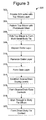
- FIG. 3 is a flow diagram of an STI scheme 300, according to an embodiment of the present invention.
- the fabrication process flow of the STI device 100 begins with the step of providing an SOI wafer with a top silicon layer 302, followed by the step of patterning the top silicon with a photoresist mask 304. Once the hardmask is formed, two separate silicon etching steps 306 are performed to form the multi-tiered body tie 104 structure. After the structures are formed, the steps of oxide deposition 308 and oxide planarization 310 are performed, after which the forming of a gate oxide and polysilicon gate layer 312 step takes place. After the formation of the gate layer, doping levels of the n+ drain 106 and n+ source 108 are established 314 by a series of implants.
- a drain contact 114, a source contact 116, a gate contact 118 and a p+ tap contact 120 are formed at the drain region 106, the source 108 region, the gate region 110 and the p+ tap region 112, respectively.
- an additional step of etching through to the body tie silicon 318 is included.
- An opening is etched through the nitride etch-stop layer down to the body tie silicon 104, after which a direct contact 122 to the body-tie 104 is formed 320.
- This adjustment to the process flow removes the requirement that a body tie contact must occur in a normal active area, which is a feature that must be lithographically designated in the active area masking and etch steps, the n+ and p+ masking and doping steps, and the implantation step.
- Figure 2a is a pictorial diagram of the cross-section cut through along the X-X' plane of the STI device configuration shown in Figure 1 .
- Buried oxide layer 202 isolates the device silicon areas 204, 208, 212 and 214 from the silicon substrate 201.
- a deposited and subsequently CMP planarized oxide 206 comprises the STI oxide isolation.
- the n+ source 208, p+ tap 212 and multi-tiered body tie 204 structures correspond to the n+ source 108 region, p+ tap 112 region, and body tie 104 region in Figure 1 , respectively.
- the multi-tiered body tie structure 204 is formed by two separate silicon etches as described above.
- a layer of silicon 214 remains after the silicon etches.
- a nitride layer 210 provides a hard mask etch stop for potential subsequent processing steps and the STI oxide layer 206 blocks the n+ and p+ source and drain implants from doping the underlying body tie silicon layer 214.
- P+ contact 220, n+ source contact 216, and direct body tie contact 222 correspond to p+ tap contact 120, n+ source contact 116 and direct body tie contact 122 in Figure 1 , respectively.
- p+ tap contact 220 and n+ source contact 216 connects to the p+ tap 212 and n+ source 208 respectively by etching through the nitride layer 210.
- the direct body tie contact 222 connects to the body tie 204 by etching through the nitride layer as well as the STI oxide layer.
- the direct body tie contact 222 is oriented vertically and of unitary construction.
- the interface of where the direct contact occurs is such that a least a portion of the direct body tie contact 222 overlays at least a portion of the body tie structure 204.
- the selectivity to the source, drain, or gate contact areas are not sufficient to etch to the body tie, then the body tie contact lithography etch can be done before the source, drain and gate contacts are formed.
- the p+ tap feature can be eliminated in this direct body tie contact configuration, since it is no longer needed. Eliminating the p+ tap feature also eliminates the need for a photoresist mask feature at a minimum design rule distance from the n-channel transistor during the n+ implant.
- Figure 2b is a pictorial diagram of the cross-section cut through along the X-X' plane of the STI device configuration shown in Figure 1 , during an n+ implant step.
- the columns 220', 216', and 222' are where contacts 220, 216 and 222 will be formed in a later step, as shown in Figure 2a .
- the photoresist 224 is necessary when a p+ tap feature is implemented, but can be left out in this alternative embodiment. As such, eliminating the p+ tap feature can improve the density as well as reduce the lithography costs of the device.
- an additional lithography and implant step can be performed after the direct body tie contact has been formed to increase the doping in the direct body tie contact to reduce contact resistance.
- the direct body tie contact implants only go into the contact areas so n+ and p+ spacing requirements are still relaxed. Note that dopant activation to improve performance can optionally occur in a typical contact TiN liner anneal step.
- the best case scenario requires no additional processing, and the worst case scenario requires one additional contact mask and etch step, and two reuses of well masks during two additional implants.
Landscapes
- Thin Film Transistor (AREA)
- Metal-Oxide And Bipolar Metal-Oxide Semiconductor Integrated Circuits (AREA)
- Internal Circuitry In Semiconductor Integrated Circuit Devices (AREA)
- Element Separation (AREA)
Applications Claiming Priority (1)
| Application Number | Priority Date | Filing Date | Title |
|---|---|---|---|
| US12/177,332 US7964897B2 (en) | 2008-07-22 | 2008-07-22 | Direct contact to area efficient body tie process flow |
Publications (1)
| Publication Number | Publication Date |
|---|---|
| EP2148362A1 true EP2148362A1 (en) | 2010-01-27 |
Family
ID=41256059
Family Applications (1)
| Application Number | Title | Priority Date | Filing Date |
|---|---|---|---|
| EP09160633A Withdrawn EP2148362A1 (en) | 2008-07-22 | 2009-05-19 | Direct contact to area efficient body tie process flow |
Country Status (4)
| Country | Link |
|---|---|
| US (1) | US7964897B2 (https=) |
| EP (1) | EP2148362A1 (https=) |
| JP (1) | JP2010045331A (https=) |
| TW (1) | TW201013791A (https=) |
Families Citing this family (2)
| Publication number | Priority date | Publication date | Assignee | Title |
|---|---|---|---|---|
| US8680617B2 (en) * | 2009-10-06 | 2014-03-25 | International Business Machines Corporation | Split level shallow trench isolation for area efficient body contacts in SOI MOSFETS |
| US9818652B1 (en) | 2016-04-27 | 2017-11-14 | Globalfoundries Inc. | Commonly-bodied field-effect transistors |
Citations (6)
| Publication number | Priority date | Publication date | Assignee | Title |
|---|---|---|---|---|
| EP0225821A2 (en) * | 1985-10-31 | 1987-06-16 | Fujitsu Limited | Semiconductor device having a silicon on insulator structure |
| DE10106423A1 (de) * | 2000-07-18 | 2002-02-07 | Mitsubishi Electric Corp | Halbleitervorrichtung |
| US20030020117A1 (en) * | 2001-07-28 | 2003-01-30 | Samsung Electronics Co., Ltd. | Silicon on insulator device having trench isolation layer and method for manufacturing the same |
| US20030025135A1 (en) * | 2001-07-17 | 2003-02-06 | Mitsubishi Denki Kabushiki Kaisha | Semiconductor device and method of manufacturing same |
| US20070181946A1 (en) * | 2006-02-08 | 2007-08-09 | Leo Mathew | Method and apparatus for forming a semiconductor-on-insulator (SOI) body-contacted device |
| US20070257317A1 (en) * | 2006-05-02 | 2007-11-08 | Honeywell International Inc. | Method of forming a body-tie |
Family Cites Families (22)
| Publication number | Priority date | Publication date | Assignee | Title |
|---|---|---|---|---|
| JPS5727070A (en) | 1980-07-25 | 1982-02-13 | Toshiba Corp | Mos type semiconductor device |
| US4786955A (en) | 1987-02-24 | 1988-11-22 | General Electric Company | Semiconductor device with source and drain depth extenders and a method of making the same |
| US5145802A (en) | 1991-11-12 | 1992-09-08 | United Technologies Corporation | Method of making SOI circuit with buried connectors |
| US5767549A (en) | 1996-07-03 | 1998-06-16 | International Business Machines Corporation | SOI CMOS structure |
| JPH10256556A (ja) * | 1997-03-14 | 1998-09-25 | Toshiba Corp | 半導体装置及びその製造方法 |
| GB9716657D0 (en) | 1997-08-07 | 1997-10-15 | Zeneca Ltd | Chemical compounds |
| DE69925078T2 (de) | 1998-08-29 | 2006-03-09 | International Business Machines Corp. | SOI-Transistor mit einem Substrat-Kontakt und Verfahren zu dessen Herstellung |
| JP2001077368A (ja) * | 1999-09-03 | 2001-03-23 | Mitsubishi Electric Corp | 半導体装置及びその製造方法 |
| US6521959B2 (en) | 1999-10-25 | 2003-02-18 | Samsung Electronics Co., Ltd. | SOI semiconductor integrated circuit for eliminating floating body effects in SOI MOSFETs and method of fabricating the same |
| KR100343288B1 (ko) | 1999-10-25 | 2002-07-15 | 윤종용 | 에스오아이 모스 트랜지스터의 플로팅 바디 효과를제거하기 위한 에스오아이 반도체 집적회로 및 그 제조방법 |
| JP2001230315A (ja) | 2000-02-17 | 2001-08-24 | Mitsubishi Electric Corp | 半導体装置およびその製造方法 |
| JP2001339071A (ja) * | 2000-03-22 | 2001-12-07 | Mitsubishi Electric Corp | 半導体装置及びその製造方法 |
| JP2002064206A (ja) * | 2000-06-09 | 2002-02-28 | Toshiba Corp | 半導体装置及びその製造方法 |
| AU2001288845A1 (en) | 2000-09-19 | 2002-04-02 | Motorola, Inc. | Body-tied silicon on insulator semiconductor device structure and method therefor |
| JP4676069B2 (ja) | 2001-02-07 | 2011-04-27 | パナソニック株式会社 | 半導体装置の製造方法 |
| US6620656B2 (en) | 2001-12-19 | 2003-09-16 | Motorola, Inc. | Method of forming body-tied silicon on insulator semiconductor device |
| US6960810B2 (en) | 2002-05-30 | 2005-11-01 | Honeywell International Inc. | Self-aligned body tie for a partially depleted SOI device structure |
| JP4154578B2 (ja) | 2002-12-06 | 2008-09-24 | 日本電気株式会社 | 半導体装置及びその製造方法 |
| US6864152B1 (en) | 2003-05-20 | 2005-03-08 | Lsi Logic Corporation | Fabrication of trenches with multiple depths on the same substrate |
| JP4811901B2 (ja) | 2004-06-03 | 2011-11-09 | ルネサスエレクトロニクス株式会社 | 半導体装置 |
| JP2006066691A (ja) * | 2004-08-27 | 2006-03-09 | Renesas Technology Corp | 半導体装置およびその製造方法 |
| US7179717B2 (en) | 2005-05-25 | 2007-02-20 | Micron Technology, Inc. | Methods of forming integrated circuit devices |
-
2008
- 2008-07-22 US US12/177,332 patent/US7964897B2/en not_active Expired - Fee Related
-
2009
- 2009-05-19 EP EP09160633A patent/EP2148362A1/en not_active Withdrawn
- 2009-05-21 TW TW098116945A patent/TW201013791A/zh unknown
- 2009-05-21 JP JP2009123064A patent/JP2010045331A/ja active Pending
Patent Citations (6)
| Publication number | Priority date | Publication date | Assignee | Title |
|---|---|---|---|---|
| EP0225821A2 (en) * | 1985-10-31 | 1987-06-16 | Fujitsu Limited | Semiconductor device having a silicon on insulator structure |
| DE10106423A1 (de) * | 2000-07-18 | 2002-02-07 | Mitsubishi Electric Corp | Halbleitervorrichtung |
| US20030025135A1 (en) * | 2001-07-17 | 2003-02-06 | Mitsubishi Denki Kabushiki Kaisha | Semiconductor device and method of manufacturing same |
| US20030020117A1 (en) * | 2001-07-28 | 2003-01-30 | Samsung Electronics Co., Ltd. | Silicon on insulator device having trench isolation layer and method for manufacturing the same |
| US20070181946A1 (en) * | 2006-02-08 | 2007-08-09 | Leo Mathew | Method and apparatus for forming a semiconductor-on-insulator (SOI) body-contacted device |
| US20070257317A1 (en) * | 2006-05-02 | 2007-11-08 | Honeywell International Inc. | Method of forming a body-tie |
Also Published As
| Publication number | Publication date |
|---|---|
| US7964897B2 (en) | 2011-06-21 |
| JP2010045331A (ja) | 2010-02-25 |
| TW201013791A (en) | 2010-04-01 |
| US20100019320A1 (en) | 2010-01-28 |
Similar Documents
| Publication | Publication Date | Title |
|---|---|---|
| TWI596711B (zh) | 塊體以及絕緣層覆矽半導體裝置之協整 | |
| US6677645B2 (en) | Body contact MOSFET | |
| US5177028A (en) | Trench isolation method having a double polysilicon gate formed on mesas | |
| US7301185B2 (en) | High-voltage transistor device having an interlayer dielectric etch stop layer for preventing leakage and improving breakdown voltage | |
| US6087208A (en) | Method for increasing gate capacitance by using both high and low dielectric gate material | |
| US6596570B2 (en) | SOI device with reduced junction capacitance | |
| JP3965064B2 (ja) | ボディ・コンタクトを有する集積回路の形成方法 | |
| US11329067B2 (en) | Co-integration of bulk and SOI transistors | |
| JP2005019996A (ja) | ハイブリッド・プレーナおよびFinFETCMOSデバイス | |
| US8680617B2 (en) | Split level shallow trench isolation for area efficient body contacts in SOI MOSFETS | |
| US6333247B1 (en) | Two-step MOSFET gate formation for high-density devices | |
| US7915110B2 (en) | MOS transistor manufacturing | |
| US9362128B2 (en) | Methods for fabricating integrated circuits and components thereof | |
| EP2148362A1 (en) | Direct contact to area efficient body tie process flow | |
| JP2017523614A (ja) | 自己整合裏面特徴部を有する半導体デバイス | |
| US9472465B2 (en) | Methods of fabricating integrated circuits | |
| US7704892B2 (en) | Semiconductor device having local interconnection layer and etch stopper pattern for preventing leakage of current | |
| US6274415B1 (en) | Self-aligned Vt implant | |
| US20020042183A1 (en) | Two-step MOSFET gate formation for high-density devices | |
| US20030119323A1 (en) | Method for fabricating transistor in semiconductor device | |
| KR100372820B1 (ko) | 이중 실리콘 모스펫 및 그 제조방법 | |
| US20030176036A1 (en) | Method of manufacturing MOS semiconductor device having PIP capacitor | |
| US12107148B2 (en) | Semiconductor devices and methods of manufacturing thereof | |
| KR100477786B1 (ko) | 반도체소자의 콘택 형성 방법 | |
| US9196544B2 (en) | Integrated circuits with stressed semiconductor-on-insulator (SOI) body contacts and methods for fabricating the same |
Legal Events
| Date | Code | Title | Description |
|---|---|---|---|
| PUAI | Public reference made under article 153(3) epc to a published international application that has entered the european phase |
Free format text: ORIGINAL CODE: 0009012 |
|
| 17P | Request for examination filed |
Effective date: 20090519 |
|
| AK | Designated contracting states |
Kind code of ref document: A1 Designated state(s): AT BE BG CH CY CZ DE DK EE ES FI FR GB GR HR HU IE IS IT LI LT LU LV MC MK MT NL NO PL PT RO SE SI SK TR |
|
| 17Q | First examination report despatched |
Effective date: 20100225 |
|
| STAA | Information on the status of an ep patent application or granted ep patent |
Free format text: STATUS: THE APPLICATION IS DEEMED TO BE WITHDRAWN |
|
| 18D | Application deemed to be withdrawn |
Effective date: 20141202 |