EP2147477B1 - Composant haute fréquence à pertes diélectriques faibles - Google Patents
Composant haute fréquence à pertes diélectriques faibles Download PDFInfo
- Publication number
- EP2147477B1 EP2147477B1 EP08748779A EP08748779A EP2147477B1 EP 2147477 B1 EP2147477 B1 EP 2147477B1 EP 08748779 A EP08748779 A EP 08748779A EP 08748779 A EP08748779 A EP 08748779A EP 2147477 B1 EP2147477 B1 EP 2147477B1
- Authority
- EP
- European Patent Office
- Prior art keywords
- frequency component
- dimensional structure
- insulating element
- component according
- film
- Prior art date
- Legal status (The legal status is an assumption and is not a legal conclusion. Google has not performed a legal analysis and makes no representation as to the accuracy of the status listed.)
- Not-in-force
Links
- 239000004020 conductor Substances 0.000 claims abstract description 48
- 238000005245 sintering Methods 0.000 claims abstract description 13
- 239000012777 electrically insulating material Substances 0.000 claims abstract description 4
- 229920001343 polytetrafluoroethylene Polymers 0.000 claims description 25
- 239000004810 polytetrafluoroethylene Substances 0.000 claims description 25
- 238000009413 insulation Methods 0.000 abstract description 31
- 239000007787 solid Substances 0.000 abstract description 7
- 238000003780 insertion Methods 0.000 abstract description 5
- 230000037431 insertion Effects 0.000 abstract description 5
- 238000004519 manufacturing process Methods 0.000 description 6
- 238000000034 method Methods 0.000 description 5
- 230000006870 function Effects 0.000 description 4
- 238000010438 heat treatment Methods 0.000 description 4
- 238000010292 electrical insulation Methods 0.000 description 3
- 239000000463 material Substances 0.000 description 3
- 230000015572 biosynthetic process Effects 0.000 description 2
- 230000000694 effects Effects 0.000 description 2
- 230000003993 interaction Effects 0.000 description 2
- 238000002955 isolation Methods 0.000 description 2
- 230000007774 longterm Effects 0.000 description 2
- 238000007493 shaping process Methods 0.000 description 2
- 238000007711 solidification Methods 0.000 description 2
- 230000008023 solidification Effects 0.000 description 2
- 238000010276 construction Methods 0.000 description 1
- 238000013016 damping Methods 0.000 description 1
- 230000001419 dependent effect Effects 0.000 description 1
- 239000012772 electrical insulation material Substances 0.000 description 1
- 238000005516 engineering process Methods 0.000 description 1
- 238000001125 extrusion Methods 0.000 description 1
- 239000007789 gas Substances 0.000 description 1
- 230000001939 inductive effect Effects 0.000 description 1
- 239000012774 insulation material Substances 0.000 description 1
- 230000003446 memory effect Effects 0.000 description 1
- 239000004033 plastic Substances 0.000 description 1
- 229920003023 plastic Polymers 0.000 description 1
- 229920006254 polymer film Polymers 0.000 description 1
- 239000002861 polymer material Substances 0.000 description 1
- -1 polytetrafluoroethylene Polymers 0.000 description 1
- 238000004080 punching Methods 0.000 description 1
- 230000005855 radiation Effects 0.000 description 1
- 239000011265 semifinished product Substances 0.000 description 1
- 238000000926 separation method Methods 0.000 description 1
Images
Classifications
-
- H—ELECTRICITY
- H01—ELECTRIC ELEMENTS
- H01P—WAVEGUIDES; RESONATORS, LINES, OR OTHER DEVICES OF THE WAVEGUIDE TYPE
- H01P1/00—Auxiliary devices
- H01P1/20—Frequency-selective devices, e.g. filters
- H01P1/213—Frequency-selective devices, e.g. filters combining or separating two or more different frequencies
-
- H—ELECTRICITY
- H01—ELECTRIC ELEMENTS
- H01P—WAVEGUIDES; RESONATORS, LINES, OR OTHER DEVICES OF THE WAVEGUIDE TYPE
- H01P3/00—Waveguides; Transmission lines of the waveguide type
- H01P3/02—Waveguides; Transmission lines of the waveguide type with two longitudinal conductors
- H01P3/08—Microstrips; Strip lines
Definitions
- the present invention relates to a high-frequency component having an inner conductor structure, which is insulated with at least one insulation element electrically against an outer conductor, wherein the insulation element mechanically supports the inner conductor structure.
- high-frequency components are frequently used, in which an internal conductor structure not only has to be insulated against the outer conductor, but also has to be mechanically supported. Examples include filters, couplers, splitters or multiplexers.
- diplexers are used between base stations and mobile radio antennas in order to be able to emit signals in different frequency ranges, for example for GSM and UMTS, via the mobile radio antennas.
- the diplexer leads to an insertion loss that should be as low as possible.
- the internal conductor structure which forms the crossover is sandwiched between two solid sheets of polytetrafluoroethylene (PTFE).
- PTFE polytetrafluoroethylene
- the material PTFE is used as insulation material in order to minimize the insertion loss caused by the diplexer.
- the two plates made of PTFE must be manufactured very precisely in thickness, in order to achieve a reliable support or fixation of the inner conductor structure in the housing. This increases the cost of manufacturing these insulation elements.
- GB 1030134 describes a hoaxia (kable with sinem inner conductor an Aupenleiter and dimen isolator, the avs laminated kvnststottsokoten besfeht.
- the object of the present invention is to provide a generic high-frequency component, which has a low insertion loss and can be produced inexpensively.
- the proposed high-frequency component has, in a known manner, an inner conductor structure which is insulated electrically with at least one insulation element against an outer conductor, wherein the insulation element mechanically supports the inner conductor structure.
- the High-frequency component is characterized in that the insulation element is formed of a formed into a three-dimensional structure and solidified by sintering with this three-dimensional structure film of an electrically insulating material, preferably a polymer material having a wall thickness which is less than a thickness caused by the three-dimensional structure of the insulating element is.
- a PTFE film shaped to the three-dimensional structure is preferably used as the insulating element.
- the thickness of this insulating element can be chosen slightly larger than required for fitting into the housing of the high-frequency component.
- the insulation element can be compressed when closing the housing to the extent just required, in which case the support or fixation of the inner conductor structure, for example, a stripline structure, is optimally ensured.
- a significant further advantage of the use of the three-dimensional structure is that the volume occupied by the insulating element has a significantly lower proportion of film material than a solid component of the same volume. Thus, the air content within this volume can be up to 90% and above.
- the damping is reduced compared to the known high-frequency components with solid insulation elements.
- the proposed high-frequency component thus has lower dielectric losses and can also be produced cost-effectively due to the lower accuracy requirements in the production of the insulation element (s).
- the three-dimensional structure is preferably formed in the present high-frequency component in a wall thickness between 50 microns and 500 microns.
- the wall thickness is of course not limited to these thickness ranges, as long as the wall thickness is less than the thickness of the insulating element.
- the mechanical stability of the insulating element is achieved with such small wall thicknesses by the special shape of the insulating element, in which the film provided in the respective film thickness, formed three-dimensionally and solidified in the three-dimensional shape by sintering. In this way, rigid edges are obtained in the three-dimensional structure, which increase the mechanical stability of the structure.
- the three-dimensionally shaped insulating element obtains a much higher form and long-term stability than the thin one by a closed, special shaping in the sintering process - the combination of rigid edges in the plane of effective loading and radially symmetric contouring transversely to the effective load Having raw film itself and in an open design sintered three-dimensional components.
- Rigid edges in the effective load plane generate a higher dimensional stability under identical load than other contours.
- the closed, radially symmetric shape perpendicular to the effective load creates a stress build-up in the direction of the contour circumference of the rigid edges without the formation of voltage spikes.
- This design reduces or eliminates the memory effect and leads to a long-term and to a critical point temperature-stable geometry of the Three-dimensional component with very thin wall thicknesses of sintered polymer films.
- the three-dimensional structure is preferably designed such that the proportion of the electrically insulating material used at the volume occupied by the insulation element is ⁇ 25%, particularly preferably ⁇ 10%. This requirement can be adjusted to a certain extent via the wall thickness and the course of the three-dimensional structure.
- the three-dimensional structure can in this case in simple cases only in one direction zig-zag or wavy. Basically, in the preferred structure, recesses and elevations alternate with one another, which, for example, can also be formed concentrically around a center. The highest areas of the elevations and / or the deepest areas of the depressions may in this case have any shapes, in particular round or angular or also be designed as planar areas. The distance of the depressions or elevations from each other can be constant or vary as needed. Furthermore, of course, more complex three-dimensional structures are possible, as long as they still ensure the required support function of the inner conductor structure.
- the outer conductor is formed by the housing of the high-frequency component or is attached to the inside of this housing, for example.
- a metallic layer As a metallic layer.
- each of these insulating elements is formed according to the present invention.
- the one insulating element may have a different structure than the other insulating element.
- identically structured insulation elements can also be arranged rotated by 90 ° or another angle about an axis in the thickness direction relative to one another in the high-frequency component, thereby improving the mechanical support of the inner conductor structure.
- the present invention can be used for different generic high-frequency components.
- the function of the component is irrelevant, as long as one or more corresponding insulation elements for electrical insulation and simultaneous support of the inner conductor structure are required.
- passive high-frequency components such as diplexers or multiplexers, RF couplers or HF splitters, high-frequency filters, etc.
- the use of the proposed insulation element to support the inner conductor structure (and arranged thereon electrical components) in active high-frequency components is possible.
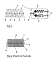
- FIG. 1 schematically an example of a high-frequency component according to the invention is shown, which is formed in this example as a diplexer.
- the internal conductor structure 2 required for the realization of a diplexer is only indicated here in a highly schematic manner.
- the person skilled in the art is familiar with the design of such an inner conductor structure for the formation of a diplexer.
- the diplexer 1 in cross-section perpendicular to the inner conductor structure 2, in the right part in section through the plane of the inner conductor structure 2 can be seen.
- the housing 3 of the diplexer forms the outer conductor.
- the output 6 and the inputs 7 of the diplexer 1 are indicated.
- the inner conductor structure 2 is between two
- Insulating elements 4, 5 embedded serve the electrical insulation between the inner conductor structure 2 and the housing 3 as an outer conductor and on the other the mechanical support of the inner conductor structure 2.
- the two insulation elements 4, 5 are formed in this example of a formed into a three-dimensional structure PTFE film 10 of a thickness of 100 microns, which has been solidified by sintering in the form of the three-dimensional structure.
- the inner conductor structure 2 is supported by these three-dimensional structures, as in the left part of FIG. 1 can be seen. Due to the spring effect of the three-dimensional structures, the thickness of each insulating element 4, 5 can be selected slightly larger than the distance between inner conductor structure 2 and GeHouseinnenwandung, in which case the insulation elements 4, 5 are slightly compressed when closing the housing 3. This allows a good fixation or support of the inner conductor structure 2 and significantly reduces the accuracy requirements for the production of the insulation elements 4, 5.
- Fig. 2 shows in comparison thereto an embodiment of such a diplexer 1 according to the prior art, in which the two insulating elements of solid PTFE plates 8, 9 are formed.
- these PTFE plates 8, 9 must be made very accurately in thickness.
- the solid PTFE plates cause a significantly greater attenuation of the high-frequency signals than the insulating elements 4, 5 of the FIG. 1 in which between the inner conductor structure 2 and the housing 3, a very high proportion of air is present. Air causes lower dielectric losses of the high frequency signals than PTFE, so that the embodiment according to FIG. 1 leads to a lower insertion loss.
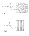
- FIG. 3 finally shows an example of a possible three-dimensional structure of the insulating elements 4 and 5, in the left part of the figure in cross section, in the right part of the figure in plan view.
- the PTFE sheet 10 is shaped to form concentric pits and bumps about a central area closed by flat plateaus.
- the distances of the elevations or depressions can be chosen differently depending on the application, in order to reliably fulfill the respective support function. This support function also depends on the thickness or Eigentragschreib the inner conductor structure.
- FIG. 4 Another example of an embodiment of such an insulation element 4, 5 shows FIG. 4 .
- the PTFE film 10 for forming the three-dimensional structure is wave-shaped in one direction, as also seen in the left part of the figure in cross section and in the right part of the figure in plan view.
- the insulation elements of the proposed high-frequency component is not limited to the structures shown here. Rather, any three-dimensional structures can be used, as long as through these structures required support of the inner conductor structure on the one hand and the required distance between the inner conductor structure and the outer conductor is ensured.
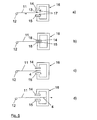
- FIG. 5 Finally, schematically shows a process sequence for producing such, three-dimensionally shaped insulating element.
- a unsintered PTFE film 11 having a thickness of 100 ⁇ m is provided on a roll 12, as can be obtained, for example, by a paste extrusion without final sintering.
- the film 11 is conveyed with the portion 13 to be formed between the punch 14 and the die 15 of a hot press 16, as shown in the FIG. 5a can be seen.
- punch 14 and die 15 are moved in a known manner against each other to bring the intermediate portion 13 of the film according to the surface structure of the punch and die in a three-dimensional shape (see. FIG. 5b ).
- This surface structure 17 is in FIG. 5 only indicated schematically.
- the section 13 of the film is heated to sintering temperature by means of heating spirals 18 integrated in the punch and die. In the present example, this heating is carried out to a temperature in the range between 350 ° and 360 ° C, which is optimal for the solidification of the film in the three-dimensional shape.
- the film portion 13 is solidified in the three-dimensional shape by sintering, in which it is held by the interaction of the punch and die.
- An expense high pressure is not required here.
- Other possibilities of heating are possible here, for example via a hot air blower or inductive.
- the film section 13 After solidification of the film section 13 by the sintering, the film section 13 is cooled. Stamp 14 and die 15 are then moved apart again as in FIG. 5c is indicated. Subsequently, the film 11 is further conveyed, so that the three-dimensionally shaped and solidified portion, the three-dimensionally shaped insulating member 4, is moved out of the hot press 16 (FIG. FIG. 5d ).
- the finished insulation element 4 can be separated from the rest of the film by suitable separation processes, for example by punching.
Landscapes
- Control Of Motors That Do Not Use Commutators (AREA)
- Coils Or Transformers For Communication (AREA)
Claims (17)
- Composant haute fréquence comportant une structure de conducteur interne (2), qui est isolée électriquement par rapport à un conducteur extérieur par au moins un élément d'isolation (4,5), dans lequel l'élément d'isolation (4,5) soutient mécaniquement la structure de conducteur interne (2),
caractérisé en ce que
l'élément d'isolation (4,5) est formé d'une feuille (10) façonnée en une structure en trois dimensions, qui a été fixée par frittage dans cette structure en trois dimensions et est formée d'un matériau isolant électriquement avec une épaisseur de paroi, qui est inférieure à une épaisseur de l'élément d'isolation (4,5) induite par la structure en trois dimensions. - Composant haute fréquence selon la revendication 1, caractérisé en ce que
l'épaisseur de paroi de la structure en trois dimensions est comprise entre 50 µm et 500 µm. - Composant haute fréquence selon la revendication 1 ou 2,
caractérisé en ce que
l'élément d'isolation (4,5) est formé d'une feuille de PTFE (10) façonnée en une structure en trois dimensions. - Composant haute fréquence selon une des revendications 1 à 3,
caractérisé en ce que
la structure en trois dimensions présente une forme en zigzag ou une forme ondulée. - Composant haute fréquence selon une des revendications 1 à 3,
caractérisé en ce que
la structure en trois dimensions forme dans au moins une direction des élévations et des renfoncements en alternance. - Composant haute fréquence selon la revendication 4 ou 5,
caractérisé en ce que
la structure en trois dimensions est réalisée de manière symétrique radialement. - Composant haute fréquence selon une des revendications 1 à 6,
caractérisé en ce que
la structure de conducteur interne (2) est incorporée en sandwich entre deux des éléments d'isolation (4,5). - Composant haute fréquence selon la revendication 7, caractérisé en ce que
les deux éléments d'isolation (4,5) présente des structures tridimensionnelles identiques et sont disposées en étant décalées d'un angle, de préférence de 90°, l'une par rapport à l'autre. - Composant haute fréquence selon une des revendications 1 à 8, qui est réalisé comme un multiplexeur, notamment comme un diplexeur.
- Composant haute fréquence selon une des revendications 1 à 8, qui est réalisé comme un filtre de hautes fréquences.
- Composant haute fréquence selon une des revendications 1 à 8, qui est réalisé comme un coupleur de hautes fréquences.
- Composant haute fréquence selon une des revendications 1 à 8, qui est réalisé comme un diviseur de hautes fréquences.
- Elément d'isolation pour composant haute fréquence selon une des revendications 1 à 12, qui est formé d'une feuille de PTFE (10) façonnée en une structure en trois dimensions, qui a été fixée par frittage dans cette structure en trois dimensions et présente une épaisseur de paroi, qui est inférieure à une épaisseur de l'élément d'isolation (4,5) induite par la structure en trois dimensions.
- Elément d'isolation selon la revendication 13, dans lequel l'épaisseur de paroi de la structure en trois dimensions est comprise entre 50 µm et 500 µm.
- Elément d'isolation selon la revendication 13 ou 14, dans lequel la structure en trois dimensions forme une forme en zigzag ou une forme ondulée.
- Elément d'isolation selon la revendication 13 ou 14, dans lequel la structure en trois dimensions forme dans au moins une direction des élévations et renfoncements en alternance.
- Elément d'isolation selon la revendication 15 ou 16, caractérisé en ce que la structure en trois dimensions est réalisée de manière symétrique radialement.
Applications Claiming Priority (2)
| Application Number | Priority Date | Filing Date | Title |
|---|---|---|---|
| DE102007019447A DE102007019447B4 (de) | 2007-04-25 | 2007-04-25 | Hochfrequenzbauteil mit geringen dielektrischen Verlusten |
| PCT/DE2008/000711 WO2008131741A1 (fr) | 2007-04-25 | 2008-04-25 | Composant haute fréquence à pertes diélectriques faibles |
Publications (2)
| Publication Number | Publication Date |
|---|---|
| EP2147477A1 EP2147477A1 (fr) | 2010-01-27 |
| EP2147477B1 true EP2147477B1 (fr) | 2011-10-26 |
Family
ID=39683530
Family Applications (1)
| Application Number | Title | Priority Date | Filing Date |
|---|---|---|---|
| EP08748779A Not-in-force EP2147477B1 (fr) | 2007-04-25 | 2008-04-25 | Composant haute fréquence à pertes diélectriques faibles |
Country Status (7)
| Country | Link |
|---|---|
| US (1) | US20100148889A1 (fr) |
| EP (1) | EP2147477B1 (fr) |
| CN (1) | CN101755363A (fr) |
| AT (1) | ATE531094T1 (fr) |
| DE (1) | DE102007019447B4 (fr) |
| ES (1) | ES2375681T3 (fr) |
| WO (1) | WO2008131741A1 (fr) |
Families Citing this family (2)
| Publication number | Priority date | Publication date | Assignee | Title |
|---|---|---|---|---|
| CN104022329B (zh) * | 2014-04-08 | 2017-11-14 | 重庆丰银包装材料有限公司 | 一种3dB电桥 |
| CN110689998B (zh) * | 2019-10-17 | 2021-12-21 | 上海幂方电子科技有限公司 | 一种可拉伸电极及其制备方法 |
Family Cites Families (23)
| Publication number | Priority date | Publication date | Assignee | Title |
|---|---|---|---|---|
| FR49795E (fr) * | 1938-09-13 | 1939-07-17 | Lignes Telegraph Telephon | Perfectionnements apportés aux conducteurs coaxiaux |
| GB537935A (en) * | 1939-07-03 | 1941-07-14 | Renato Finzi Contini | Crossed strip insulating structure for concentric cables |
| BE480485A (fr) * | 1945-09-07 | |||
| GB707966A (en) * | 1950-01-26 | 1954-04-28 | Rolls Royce | Improvements in or relating to articles consisting essentially of a polymer of tetrafluoroethylene and to the manufacture thereof |
| DE972318C (de) * | 1952-12-11 | 1959-07-02 | Telefunken Gmbh | Brueckenanordnung fuer sehr kurze elektrische Wellen |
| GB1030134A (en) * | 1962-09-28 | 1966-05-18 | Furukawa Electric Co Ltd | Coaxial cables |
| DE1248761B (fr) * | 1962-11-20 | |||
| GB1053155A (fr) * | 1964-04-30 | |||
| DE1640696A1 (de) * | 1967-05-26 | 1970-10-29 | Kabel Metallwerke Ghh | Koaxiales Hochfrequenzkabel mit Hohlraumisolierung |
| GB1185232A (en) * | 1967-09-07 | 1970-03-25 | British Insulated Callenders | Improvements in or relating to Coaxial Cables for the Transmission of High Frequency Electric Currents |
| GB1278219A (en) * | 1971-01-28 | 1972-06-21 | Standard Telephones Cables Ltd | Cables |
| GB1390809A (en) * | 1972-08-05 | 1975-04-16 | Marconi Co Ltd | Electrical networks for use at high frequencies |
| FR2374153A1 (fr) * | 1976-12-20 | 1978-07-13 | Ici Ltd | Procede pour la production d'objets en polytetrafluorethylene poreux |
| GB1605120A (en) * | 1978-04-11 | 1981-12-16 | Marconi Co Ltd | Electrical networks for use at high frequencies |
| US4463329A (en) * | 1978-08-15 | 1984-07-31 | Hirosuke Suzuki | Dielectric waveguide |
| US4427953A (en) * | 1981-11-16 | 1984-01-24 | Hughes Aircraft Company | Microwave diplexer |
| US5406235A (en) * | 1990-12-26 | 1995-04-11 | Tdk Corporation | High frequency device |
| GB9510829D0 (en) * | 1995-05-22 | 1995-07-19 | Racal Mesl Radar Limited | Radio frequency coupler |
| WO2004079795A2 (fr) * | 2003-03-04 | 2004-09-16 | Rohm And Haas Electronic Materials, L.L.C. | Microstructures a guide d'ondes coaxial et leur procede de formation |
| US6882242B2 (en) * | 2003-06-19 | 2005-04-19 | Radio Frequency Systems, Inc. | Frequency selective low loss transmission line system |
| AT501770B1 (de) * | 2005-04-07 | 2007-10-15 | Michel Wolfgang Ing | Verfahren zur herstellung einer profilierten bahn aus polytetrafluorethylen |
| DE202006010828U1 (de) * | 2006-05-15 | 2006-10-12 | Elringklinger Ag | Vorrichtung zum Herstellen einer profilierten Folie sowie mit der Vorrichtung hergestellte Folie |
| JP2008182340A (ja) * | 2007-01-23 | 2008-08-07 | Ngk Spark Plug Co Ltd | ダイプレクサ及びそれを用いたマルチプレクサ |
-
2007
- 2007-04-25 DE DE102007019447A patent/DE102007019447B4/de not_active Expired - Fee Related
-
2008
- 2008-04-25 CN CN200880017541A patent/CN101755363A/zh active Pending
- 2008-04-25 EP EP08748779A patent/EP2147477B1/fr not_active Not-in-force
- 2008-04-25 AT AT08748779T patent/ATE531094T1/de active
- 2008-04-25 US US12/597,040 patent/US20100148889A1/en not_active Abandoned
- 2008-04-25 WO PCT/DE2008/000711 patent/WO2008131741A1/fr not_active Ceased
- 2008-04-25 ES ES08748779T patent/ES2375681T3/es active Active
Also Published As
| Publication number | Publication date |
|---|---|
| ES2375681T3 (es) | 2012-03-05 |
| DE102007019447B4 (de) | 2009-05-07 |
| US20100148889A1 (en) | 2010-06-17 |
| DE102007019447A1 (de) | 2008-11-13 |
| EP2147477A1 (fr) | 2010-01-27 |
| CN101755363A (zh) | 2010-06-23 |
| WO2008131741A1 (fr) | 2008-11-06 |
| ATE531094T1 (de) | 2011-11-15 |
Similar Documents
| Publication | Publication Date | Title |
|---|---|---|
| DE69027171T2 (de) | Elektrische Inspektionseinheit mit einer anisotropischen elektrisch leitenden Schicht und Verfahren zur Herstellung der anisotropischen elektrisch leitenden Schicht | |
| DE102018121461A1 (de) | Spulenkomponente | |
| EP4009440B1 (fr) | Paroi de radôme pour les applications de communication | |
| EP3451441B1 (fr) | Filtre coaxial | |
| EP2147477B1 (fr) | Composant haute fréquence à pertes diélectriques faibles | |
| DE3708569A1 (de) | Waermeisolatormaterial und verfahren zu seiner herstellung | |
| DE10215993B4 (de) | Verfahren zur Herstellung eines Keramikschichtkörpers | |
| EP1214480A1 (fr) | Corps moule d'isolation et procede de fabrication dudit corps | |
| EP1129493B1 (fr) | Structure multicouche piezoceramique presentant une surface de section polygonale | |
| AT1045U1 (de) | Spulenkörper und verfahren zu dessen herstellung für einen transformator | |
| DE2203206A1 (de) | Warzenplatte mit offenen Zellen,zur Herstellung von Bauplatten,Waenden u.dgl. geeignet,sowie Verfahren zur Herstellung derselben | |
| DE102019132543A1 (de) | Magnetkern aus nanokristallinem laminat für ein induktives bauelement | |
| EP1910071B1 (fr) | Corps deformable a faible poids specifique | |
| DE102017108384A1 (de) | Vielschichtbauelement und Verfahren zur Herstellung eines Vielschichtbauelements | |
| DE4434658C2 (de) | Dämmplatte und Verfahren zur Herstellung einer Dämmplatte | |
| DE202008016388U1 (de) | Kapazitiver Leitungskoppler | |
| EP1759191B1 (fr) | Configuration d'un element et d'un dispositif de controle de cet element, procede pour realiser cette configuration et utilisation de cette configuration | |
| WO1998026928A1 (fr) | Corps moules calorifuges pourvus d'un enrobage et leur procede de production | |
| EP3358674B1 (fr) | Dispositif d'antenne souple | |
| EP3385957A1 (fr) | Bande d'isolation électrique, machine électrique haute tension et procédé de fabrication d'une bande d'isolation électrique et machine électrique haute tension | |
| DE102019007023B4 (de) | Strukturbauteil und Verfahren zu dessen Herstellung | |
| DE2854173A1 (de) | Vorrichtung zur haertung von formstuecken aus mit kunststoff benetzten oder getraenkten fuellstoffen | |
| WO2019201503A1 (fr) | Ligne de transmission de signaux | |
| WO2003005444A2 (fr) | Substrats polymeres a noyau de ceramique destines a etre utilises dans la technique haute frequence | |
| DE2339775C3 (de) | Hochfrequenzverteiler, insbesondere für Fernsehantennen |
Legal Events
| Date | Code | Title | Description |
|---|---|---|---|
| PUAI | Public reference made under article 153(3) epc to a published international application that has entered the european phase |
Free format text: ORIGINAL CODE: 0009012 |
|
| 17P | Request for examination filed |
Effective date: 20091111 |
|
| AK | Designated contracting states |
Kind code of ref document: A1 Designated state(s): AT BE BG CH CY CZ DE DK EE ES FI FR GB GR HR HU IE IS IT LI LT LU LV MC MT NL NO PL PT RO SE SI SK TR |
|
| AX | Request for extension of the european patent |
Extension state: AL BA MK RS |
|
| DAX | Request for extension of the european patent (deleted) | ||
| GRAP | Despatch of communication of intention to grant a patent |
Free format text: ORIGINAL CODE: EPIDOSNIGR1 |
|
| GRAS | Grant fee paid |
Free format text: ORIGINAL CODE: EPIDOSNIGR3 |
|
| GRAA | (expected) grant |
Free format text: ORIGINAL CODE: 0009210 |
|
| AK | Designated contracting states |
Kind code of ref document: B1 Designated state(s): AT BE BG CH CY CZ DE DK EE ES FI FR GB GR HR HU IE IS IT LI LT LU LV MC MT NL NO PL PT RO SE SI SK TR |
|
| REG | Reference to a national code |
Ref country code: GB Ref legal event code: FG4D Free format text: NOT ENGLISH |
|
| REG | Reference to a national code |
Ref country code: CH Ref legal event code: EP |
|
| REG | Reference to a national code |
Ref country code: IE Ref legal event code: FG4D |
|
| REG | Reference to a national code |
Ref country code: DE Ref legal event code: R096 Ref document number: 502008005377 Country of ref document: DE Effective date: 20120105 |
|
| REG | Reference to a national code |
Ref country code: SE Ref legal event code: TRGR |
|
| REG | Reference to a national code |
Ref country code: NL Ref legal event code: VDEP Effective date: 20111026 |
|
| REG | Reference to a national code |
Ref country code: ES Ref legal event code: FG2A Ref document number: 2375681 Country of ref document: ES Kind code of ref document: T3 Effective date: 20120305 |
|
| LTIE | Lt: invalidation of european patent or patent extension |
Effective date: 20111026 |
|
| PG25 | Lapsed in a contracting state [announced via postgrant information from national office to epo] |
Ref country code: IS Free format text: LAPSE BECAUSE OF FAILURE TO SUBMIT A TRANSLATION OF THE DESCRIPTION OR TO PAY THE FEE WITHIN THE PRESCRIBED TIME-LIMIT Effective date: 20120226 Ref country code: LT Free format text: LAPSE BECAUSE OF FAILURE TO SUBMIT A TRANSLATION OF THE DESCRIPTION OR TO PAY THE FEE WITHIN THE PRESCRIBED TIME-LIMIT Effective date: 20111026 Ref country code: NO Free format text: LAPSE BECAUSE OF FAILURE TO SUBMIT A TRANSLATION OF THE DESCRIPTION OR TO PAY THE FEE WITHIN THE PRESCRIBED TIME-LIMIT Effective date: 20120126 |
|
| PG25 | Lapsed in a contracting state [announced via postgrant information from national office to epo] |
Ref country code: HR Free format text: LAPSE BECAUSE OF FAILURE TO SUBMIT A TRANSLATION OF THE DESCRIPTION OR TO PAY THE FEE WITHIN THE PRESCRIBED TIME-LIMIT Effective date: 20111026 Ref country code: NL Free format text: LAPSE BECAUSE OF FAILURE TO SUBMIT A TRANSLATION OF THE DESCRIPTION OR TO PAY THE FEE WITHIN THE PRESCRIBED TIME-LIMIT Effective date: 20111026 Ref country code: GR Free format text: LAPSE BECAUSE OF FAILURE TO SUBMIT A TRANSLATION OF THE DESCRIPTION OR TO PAY THE FEE WITHIN THE PRESCRIBED TIME-LIMIT Effective date: 20120127 Ref country code: PT Free format text: LAPSE BECAUSE OF FAILURE TO SUBMIT A TRANSLATION OF THE DESCRIPTION OR TO PAY THE FEE WITHIN THE PRESCRIBED TIME-LIMIT Effective date: 20120227 Ref country code: SI Free format text: LAPSE BECAUSE OF FAILURE TO SUBMIT A TRANSLATION OF THE DESCRIPTION OR TO PAY THE FEE WITHIN THE PRESCRIBED TIME-LIMIT Effective date: 20111026 Ref country code: PL Free format text: LAPSE BECAUSE OF FAILURE TO SUBMIT A TRANSLATION OF THE DESCRIPTION OR TO PAY THE FEE WITHIN THE PRESCRIBED TIME-LIMIT Effective date: 20111026 Ref country code: LV Free format text: LAPSE BECAUSE OF FAILURE TO SUBMIT A TRANSLATION OF THE DESCRIPTION OR TO PAY THE FEE WITHIN THE PRESCRIBED TIME-LIMIT Effective date: 20111026 |
|
| REG | Reference to a national code |
Ref country code: IE Ref legal event code: FD4D |
|
| PG25 | Lapsed in a contracting state [announced via postgrant information from national office to epo] |
Ref country code: CY Free format text: LAPSE BECAUSE OF FAILURE TO SUBMIT A TRANSLATION OF THE DESCRIPTION OR TO PAY THE FEE WITHIN THE PRESCRIBED TIME-LIMIT Effective date: 20111026 |
|
| PG25 | Lapsed in a contracting state [announced via postgrant information from national office to epo] |
Ref country code: SK Free format text: LAPSE BECAUSE OF FAILURE TO SUBMIT A TRANSLATION OF THE DESCRIPTION OR TO PAY THE FEE WITHIN THE PRESCRIBED TIME-LIMIT Effective date: 20111026 Ref country code: EE Free format text: LAPSE BECAUSE OF FAILURE TO SUBMIT A TRANSLATION OF THE DESCRIPTION OR TO PAY THE FEE WITHIN THE PRESCRIBED TIME-LIMIT Effective date: 20111026 Ref country code: CZ Free format text: LAPSE BECAUSE OF FAILURE TO SUBMIT A TRANSLATION OF THE DESCRIPTION OR TO PAY THE FEE WITHIN THE PRESCRIBED TIME-LIMIT Effective date: 20111026 Ref country code: BG Free format text: LAPSE BECAUSE OF FAILURE TO SUBMIT A TRANSLATION OF THE DESCRIPTION OR TO PAY THE FEE WITHIN THE PRESCRIBED TIME-LIMIT Effective date: 20120126 Ref country code: IE Free format text: LAPSE BECAUSE OF FAILURE TO SUBMIT A TRANSLATION OF THE DESCRIPTION OR TO PAY THE FEE WITHIN THE PRESCRIBED TIME-LIMIT Effective date: 20111026 Ref country code: DK Free format text: LAPSE BECAUSE OF FAILURE TO SUBMIT A TRANSLATION OF THE DESCRIPTION OR TO PAY THE FEE WITHIN THE PRESCRIBED TIME-LIMIT Effective date: 20111026 |
|
| PG25 | Lapsed in a contracting state [announced via postgrant information from national office to epo] |
Ref country code: RO Free format text: LAPSE BECAUSE OF FAILURE TO SUBMIT A TRANSLATION OF THE DESCRIPTION OR TO PAY THE FEE WITHIN THE PRESCRIBED TIME-LIMIT Effective date: 20111026 |
|
| PLBE | No opposition filed within time limit |
Free format text: ORIGINAL CODE: 0009261 |
|
| STAA | Information on the status of an ep patent application or granted ep patent |
Free format text: STATUS: NO OPPOSITION FILED WITHIN TIME LIMIT |
|
| 26N | No opposition filed |
Effective date: 20120727 |
|
| BERE | Be: lapsed |
Owner name: SPINNER G.M.B.H. Effective date: 20120430 |
|
| REG | Reference to a national code |
Ref country code: DE Ref legal event code: R097 Ref document number: 502008005377 Country of ref document: DE Effective date: 20120727 |
|
| PG25 | Lapsed in a contracting state [announced via postgrant information from national office to epo] |
Ref country code: MC Free format text: LAPSE BECAUSE OF NON-PAYMENT OF DUE FEES Effective date: 20120430 |
|
| REG | Reference to a national code |
Ref country code: CH Ref legal event code: PL |
|
| GBPC | Gb: european patent ceased through non-payment of renewal fee |
Effective date: 20120425 |
|
| PG25 | Lapsed in a contracting state [announced via postgrant information from national office to epo] |
Ref country code: BE Free format text: LAPSE BECAUSE OF NON-PAYMENT OF DUE FEES Effective date: 20120430 Ref country code: GB Free format text: LAPSE BECAUSE OF NON-PAYMENT OF DUE FEES Effective date: 20120425 Ref country code: LI Free format text: LAPSE BECAUSE OF NON-PAYMENT OF DUE FEES Effective date: 20120430 Ref country code: CH Free format text: LAPSE BECAUSE OF NON-PAYMENT OF DUE FEES Effective date: 20120430 |
|
| PGFP | Annual fee paid to national office [announced via postgrant information from national office to epo] |
Ref country code: ES Payment date: 20130315 Year of fee payment: 6 |
|
| PG25 | Lapsed in a contracting state [announced via postgrant information from national office to epo] |
Ref country code: MT Free format text: LAPSE BECAUSE OF FAILURE TO SUBMIT A TRANSLATION OF THE DESCRIPTION OR TO PAY THE FEE WITHIN THE PRESCRIBED TIME-LIMIT Effective date: 20111026 |
|
| PGFP | Annual fee paid to national office [announced via postgrant information from national office to epo] |
Ref country code: DE Payment date: 20130420 Year of fee payment: 6 Ref country code: SE Payment date: 20130416 Year of fee payment: 6 |
|
| PGFP | Annual fee paid to national office [announced via postgrant information from national office to epo] |
Ref country code: FR Payment date: 20130527 Year of fee payment: 6 Ref country code: FI Payment date: 20130409 Year of fee payment: 6 Ref country code: IT Payment date: 20130424 Year of fee payment: 6 |
|
| PG25 | Lapsed in a contracting state [announced via postgrant information from national office to epo] |
Ref country code: TR Free format text: LAPSE BECAUSE OF FAILURE TO SUBMIT A TRANSLATION OF THE DESCRIPTION OR TO PAY THE FEE WITHIN THE PRESCRIBED TIME-LIMIT Effective date: 20111026 |
|
| PG25 | Lapsed in a contracting state [announced via postgrant information from national office to epo] |
Ref country code: LU Free format text: LAPSE BECAUSE OF NON-PAYMENT OF DUE FEES Effective date: 20120425 |
|
| REG | Reference to a national code |
Ref country code: AT Ref legal event code: MM01 Ref document number: 531094 Country of ref document: AT Kind code of ref document: T Effective date: 20130425 |
|
| PG25 | Lapsed in a contracting state [announced via postgrant information from national office to epo] |
Ref country code: HU Free format text: LAPSE BECAUSE OF FAILURE TO SUBMIT A TRANSLATION OF THE DESCRIPTION OR TO PAY THE FEE WITHIN THE PRESCRIBED TIME-LIMIT Effective date: 20080425 |
|
| PG25 | Lapsed in a contracting state [announced via postgrant information from national office to epo] |
Ref country code: AT Free format text: LAPSE BECAUSE OF NON-PAYMENT OF DUE FEES Effective date: 20130425 |
|
| REG | Reference to a national code |
Ref country code: DE Ref legal event code: R119 Ref document number: 502008005377 Country of ref document: DE |
|
| REG | Reference to a national code |
Ref country code: SE Ref legal event code: EUG |
|
| REG | Reference to a national code |
Ref country code: DE Ref legal event code: R119 Ref document number: 502008005377 Country of ref document: DE Effective date: 20141101 |
|
| REG | Reference to a national code |
Ref country code: FR Ref legal event code: ST Effective date: 20141231 |
|
| PG25 | Lapsed in a contracting state [announced via postgrant information from national office to epo] |
Ref country code: DE Free format text: LAPSE BECAUSE OF NON-PAYMENT OF DUE FEES Effective date: 20141101 Ref country code: FI Free format text: LAPSE BECAUSE OF NON-PAYMENT OF DUE FEES Effective date: 20140425 Ref country code: SE Free format text: LAPSE BECAUSE OF NON-PAYMENT OF DUE FEES Effective date: 20140426 |
|
| PG25 | Lapsed in a contracting state [announced via postgrant information from national office to epo] |
Ref country code: FR Free format text: LAPSE BECAUSE OF NON-PAYMENT OF DUE FEES Effective date: 20140430 |
|
| PG25 | Lapsed in a contracting state [announced via postgrant information from national office to epo] |
Ref country code: IT Free format text: LAPSE BECAUSE OF NON-PAYMENT OF DUE FEES Effective date: 20140425 |
|
| REG | Reference to a national code |
Ref country code: ES Ref legal event code: FD2A Effective date: 20151002 |
|
| PG25 | Lapsed in a contracting state [announced via postgrant information from national office to epo] |
Ref country code: ES Free format text: LAPSE BECAUSE OF NON-PAYMENT OF DUE FEES Effective date: 20140426 |