EP2144292A2 - Display aus organischen Leuchtdioden und dessen Herstellungsmethode - Google Patents
Display aus organischen Leuchtdioden und dessen Herstellungsmethode Download PDFInfo
- Publication number
- EP2144292A2 EP2144292A2 EP09165021A EP09165021A EP2144292A2 EP 2144292 A2 EP2144292 A2 EP 2144292A2 EP 09165021 A EP09165021 A EP 09165021A EP 09165021 A EP09165021 A EP 09165021A EP 2144292 A2 EP2144292 A2 EP 2144292A2
- Authority
- EP
- European Patent Office
- Prior art keywords
- layer
- electrode
- groove
- pixel define
- intermediate layer
- Prior art date
- Legal status (The legal status is an assumption and is not a legal conclusion. Google has not performed a legal analysis and makes no representation as to the accuracy of the status listed.)
- Withdrawn
Links
Images


Classifications
-
- H—ELECTRICITY
- H10—SEMICONDUCTOR DEVICES; ELECTRIC SOLID-STATE DEVICES NOT OTHERWISE PROVIDED FOR
- H10K—ORGANIC ELECTRIC SOLID-STATE DEVICES
- H10K59/00—Integrated devices, or assemblies of multiple devices, comprising at least one organic light-emitting element covered by group H10K50/00
- H10K59/10—OLED displays
- H10K59/12—Active-matrix OLED [AMOLED] displays
- H10K59/122—Pixel-defining structures or layers, e.g. banks
-
- H—ELECTRICITY
- H10—SEMICONDUCTOR DEVICES; ELECTRIC SOLID-STATE DEVICES NOT OTHERWISE PROVIDED FOR
- H10K—ORGANIC ELECTRIC SOLID-STATE DEVICES
- H10K59/00—Integrated devices, or assemblies of multiple devices, comprising at least one organic light-emitting element covered by group H10K50/00
- H10K59/10—OLED displays
- H10K59/12—Active-matrix OLED [AMOLED] displays
- H10K59/124—Insulating layers formed between TFT elements and OLED elements
-
- H—ELECTRICITY
- H10—SEMICONDUCTOR DEVICES; ELECTRIC SOLID-STATE DEVICES NOT OTHERWISE PROVIDED FOR
- H10K—ORGANIC ELECTRIC SOLID-STATE DEVICES
- H10K85/00—Organic materials used in the body or electrodes of devices covered by this subclass
- H10K85/10—Organic polymers or oligomers
- H10K85/111—Organic polymers or oligomers comprising aromatic, heteroaromatic, or aryl chains, e.g. polyaniline, polyphenylene or polyphenylene vinylene
- H10K85/113—Heteroaromatic compounds comprising sulfur or selene, e.g. polythiophene
- H10K85/1135—Polyethylene dioxythiophene [PEDOT]; Derivatives thereof
-
- H—ELECTRICITY
- H10—SEMICONDUCTOR DEVICES; ELECTRIC SOLID-STATE DEVICES NOT OTHERWISE PROVIDED FOR
- H10K—ORGANIC ELECTRIC SOLID-STATE DEVICES
- H10K85/00—Organic materials used in the body or electrodes of devices covered by this subclass
- H10K85/10—Organic polymers or oligomers
- H10K85/111—Organic polymers or oligomers comprising aromatic, heteroaromatic, or aryl chains, e.g. polyaniline, polyphenylene or polyphenylene vinylene
- H10K85/114—Poly-phenylenevinylene; Derivatives thereof
-
- H—ELECTRICITY
- H10—SEMICONDUCTOR DEVICES; ELECTRIC SOLID-STATE DEVICES NOT OTHERWISE PROVIDED FOR
- H10K—ORGANIC ELECTRIC SOLID-STATE DEVICES
- H10K85/00—Organic materials used in the body or electrodes of devices covered by this subclass
- H10K85/10—Organic polymers or oligomers
- H10K85/111—Organic polymers or oligomers comprising aromatic, heteroaromatic, or aryl chains, e.g. polyaniline, polyphenylene or polyphenylene vinylene
- H10K85/115—Polyfluorene; Derivatives thereof
-
- H—ELECTRICITY
- H10—SEMICONDUCTOR DEVICES; ELECTRIC SOLID-STATE DEVICES NOT OTHERWISE PROVIDED FOR
- H10K—ORGANIC ELECTRIC SOLID-STATE DEVICES
- H10K85/00—Organic materials used in the body or electrodes of devices covered by this subclass
- H10K85/30—Coordination compounds
- H10K85/311—Phthalocyanine
-
- C—CHEMISTRY; METALLURGY
- C08—ORGANIC MACROMOLECULAR COMPOUNDS; THEIR PREPARATION OR CHEMICAL WORKING-UP; COMPOSITIONS BASED THEREON
- C08G—MACROMOLECULAR COMPOUNDS OBTAINED OTHERWISE THAN BY REACTIONS ONLY INVOLVING UNSATURATED CARBON-TO-CARBON BONDS
- C08G2261/00—Macromolecular compounds obtained by reactions forming a carbon-to-carbon link in the main chain of the macromolecule
- C08G2261/10—Definition of the polymer structure
- C08G2261/14—Side-groups
- C08G2261/142—Side-chains containing oxygen
- C08G2261/1424—Side-chains containing oxygen containing ether groups, including alkoxy
-
- C—CHEMISTRY; METALLURGY
- C08—ORGANIC MACROMOLECULAR COMPOUNDS; THEIR PREPARATION OR CHEMICAL WORKING-UP; COMPOSITIONS BASED THEREON
- C08G—MACROMOLECULAR COMPOUNDS OBTAINED OTHERWISE THAN BY REACTIONS ONLY INVOLVING UNSATURATED CARBON-TO-CARBON BONDS
- C08G2261/00—Macromolecular compounds obtained by reactions forming a carbon-to-carbon link in the main chain of the macromolecule
- C08G2261/30—Monomer units or repeat units incorporating structural elements in the main chain
- C08G2261/31—Monomer units or repeat units incorporating structural elements in the main chain incorporating aromatic structural elements in the main chain
- C08G2261/314—Condensed aromatic systems, e.g. perylene, anthracene or pyrene
- C08G2261/3142—Condensed aromatic systems, e.g. perylene, anthracene or pyrene fluorene-based, e.g. fluorene, indenofluorene, or spirobifluorene
-
- C—CHEMISTRY; METALLURGY
- C08—ORGANIC MACROMOLECULAR COMPOUNDS; THEIR PREPARATION OR CHEMICAL WORKING-UP; COMPOSITIONS BASED THEREON
- C08G—MACROMOLECULAR COMPOUNDS OBTAINED OTHERWISE THAN BY REACTIONS ONLY INVOLVING UNSATURATED CARBON-TO-CARBON BONDS
- C08G2261/00—Macromolecular compounds obtained by reactions forming a carbon-to-carbon link in the main chain of the macromolecule
- C08G2261/30—Monomer units or repeat units incorporating structural elements in the main chain
- C08G2261/32—Monomer units or repeat units incorporating structural elements in the main chain incorporating heteroaromatic structural elements in the main chain
- C08G2261/322—Monomer units or repeat units incorporating structural elements in the main chain incorporating heteroaromatic structural elements in the main chain non-condensed
- C08G2261/3221—Monomer units or repeat units incorporating structural elements in the main chain incorporating heteroaromatic structural elements in the main chain non-condensed containing one or more nitrogen atoms as the only heteroatom, e.g. pyrrole, pyridine or triazole
-
- C—CHEMISTRY; METALLURGY
- C08—ORGANIC MACROMOLECULAR COMPOUNDS; THEIR PREPARATION OR CHEMICAL WORKING-UP; COMPOSITIONS BASED THEREON
- C08G—MACROMOLECULAR COMPOUNDS OBTAINED OTHERWISE THAN BY REACTIONS ONLY INVOLVING UNSATURATED CARBON-TO-CARBON BONDS
- C08G2261/00—Macromolecular compounds obtained by reactions forming a carbon-to-carbon link in the main chain of the macromolecule
- C08G2261/30—Monomer units or repeat units incorporating structural elements in the main chain
- C08G2261/32—Monomer units or repeat units incorporating structural elements in the main chain incorporating heteroaromatic structural elements in the main chain
- C08G2261/322—Monomer units or repeat units incorporating structural elements in the main chain incorporating heteroaromatic structural elements in the main chain non-condensed
- C08G2261/3223—Monomer units or repeat units incorporating structural elements in the main chain incorporating heteroaromatic structural elements in the main chain non-condensed containing one or more sulfur atoms as the only heteroatom, e.g. thiophene
-
- C—CHEMISTRY; METALLURGY
- C08—ORGANIC MACROMOLECULAR COMPOUNDS; THEIR PREPARATION OR CHEMICAL WORKING-UP; COMPOSITIONS BASED THEREON
- C08G—MACROMOLECULAR COMPOUNDS OBTAINED OTHERWISE THAN BY REACTIONS ONLY INVOLVING UNSATURATED CARBON-TO-CARBON BONDS
- C08G2261/00—Macromolecular compounds obtained by reactions forming a carbon-to-carbon link in the main chain of the macromolecule
- C08G2261/30—Monomer units or repeat units incorporating structural elements in the main chain
- C08G2261/34—Monomer units or repeat units incorporating structural elements in the main chain incorporating partially-aromatic structural elements in the main chain
- C08G2261/342—Monomer units or repeat units incorporating structural elements in the main chain incorporating partially-aromatic structural elements in the main chain containing only carbon atoms
- C08G2261/3422—Monomer units or repeat units incorporating structural elements in the main chain incorporating partially-aromatic structural elements in the main chain containing only carbon atoms conjugated, e.g. PPV-type
Definitions
- the present invention relates to an organic light emitting diode (OLED) display apparatus and a method of manufacturing the same and, more particularly, to an OLED display apparatus that enables an organic emissive layer to be easily formed.
- OLED organic light emitting diode
- OLED display apparatuses including a light-emitting layer formed of an organic material have better brightness, lower driving voltage, and faster response time than inorganic light emitting display apparatuses, while providing multicolored images.
- An OLED display apparatus includes an organic emissive device having a cathode and an anode placed in conjunction with an organic emissive layer.
- an organic emissive device having a cathode and an anode placed in conjunction with an organic emissive layer.
- a voltage is applied between the cathode and the anode, visible light is obtained by the organic emissive layer connected to the cathode and the anode. Since electric charges are supplied to the organic emissive layer via the cathode and the anode, the contact between the organic emissive layer and the cathode or the anode influences the optical properties of the OLED display apparatus.
- Embodiments are therefore directed to an OLED display apparatus and method of manufacturing the same.
- an OLED display apparatus including a substrate, at least one thin film transistor (TFT) on the substrate, an insulating layer covering the at least one TFT and having a via hole and a groove, a first electrode on the insulating layer and electrically connected to the at least one TFT through the via hole, a pixel define layer on the first electrode and the groove, the pixel define layer having an opening that exposes the first electrode, an intermediate layer electrically connected to the first electrode through the opening, the intermediate layer including an organic emissive layer and, a second electrode on the intermediate layer.
- TFT thin film transistor
- the groove may be between two adjacent TFTs.
- a plurality of the grooves may be between two adjacent TFTs.
- the groove may have a depth of about 0.5 ⁇ m to about 1.5 ⁇ m.
- the groove may extend horizontally on the insulating layer.
- At least one of the above and other features and advantages may also be realized by providing a method of manufacturing an OLED display apparatus, the method including preparing a substrate, forming at least one TFT on the substrate, forming an insulating layer to cover the at least one TFT, forming a via hole and a groove in the insulating layer, forming a first electrode on the insulating layer and electrically connected to the at least one TFT through the via hole, forming a pixel define layer on the first electrode, the pixel define layer having an opening that exposes the first electrode, forming an intermediate layer electrically connected to the first electrode through the opening, the intermediate layer including an organic emissive layer and, forming a second electrode on the intermediate layer.
- the intermediate layer may be formed using a thermal transfer method.
- the via hole and the groove may be simultaneously patterned using a single mask.
- a portion of the pixel define layer may fill the groove.
- the groove may be formed between two adjacent TFTs.
- a plurality of grooves may be formed between two adjacent TFTs.
- the groove may extend horizontally on the insulating layer.
- the groove may have a depth of about 0.5 ⁇ m to about 1.5 ⁇ m.
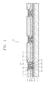
- FIG. 1 illustrates a cross-sectional view of an OLED display apparatus 100 according to an embodiment.
- the OLED display apparatus 100 may include a substrate 101, a thin film transistor (TFT), an insulating layer 110, an organic emissive device 130, and a pixel define layer 120.
- the organic emissive device 130 may include a first electrode 131, an intermediate layer 132, and a second electrode 133.
- the substrate 101 may be formed of a transparent glass material having SiO2 as a main component.
- a material for forming the substrate 101 may not be limited to the transparent glass and may be a transparent plastic material.
- the transparent plastic material may be an insulating organic material that may include at least one of polyethersulfone (PES), polyacrylate (PAR), polyetherimide (PEI), polyethylene naphthalate (PEN), polyethyleneterepthalate (PET), polyphenylene sulfide (PPS), polyallylate, polyimide, polycarbonate (PC), cellulose triacetate (TAC) and cellulose acetate propionate (CAP).
- PES polyethersulfone
- PAR polyacrylate
- PEI polyetherimide
- PEN polyethylene naphthalate
- PET polyethyleneterepthalate
- PPS polyphenylene sulfide
- PC polycarbonate
- TAC cellulose triacetate
- CAP cellulose acetate propionate
- the substrate 101 may be formed of a transparent material.
- the substrate 101 may not be required to be formed of a transparent material. That is, the substrate 101 may be formed of a metal layer, e.g., a metal foil.
- the substrate 101 may include at least one of iron, chromium, manganese, nickel, titanium, molybdenum, steel use stainless (SUS), Invar alloy, Inconel alloy, or Kovar alloy, but is not limited thereto.
- a buffer layer 102 may be formed on the substrate 101 to make the substrate 101 smooth and to prevent the penetration of impurities into the substrate 101.
- the buffer layer 102 may be formed of SiO 2 and/oi SiN x .
- the TFT may be formed on the buffer layer 102. At least one TFT may be formed for each pixel and may be electrically connected to the organic emissive device 130. For convenience of description, three TFTs are illustrated in FIG. 1 , but the embodiment is not limited thereto.
- an active layer 103 having a predetermined pattern may be formed on the buffer layer 102.
- the active layer 103 may be formed of an inorganic semiconductor, e.g., amorphous silicon or polysilicon, or an organic semiconductor, and may include a source region, a drain region, and a channel region.
- the source and the drain regions may be formed by doping the active layer 103 formed of amorphous silicon or polysilicon with impurities.
- the active layer 103 may be doped with boron, an element of Group 3, thereby forming a p-type semiconductor.
- the active layer 103 may be doped with nitrogen, an element of Group 5, thereby forming an n-type semiconductor.
- a gate insulating layer 104 may be formed on the active layer 103.
- the gate insulating layer 104 may be formed of an organic material or an inorganic material, e.g., SiNx or SiO2, and may insulate the active layer 103 from a gate electrode 105.
- the gate electrode 105 may be formed on a predetermined portion of the gate insulating layer 104.
- the gate electrode 105 may be formed of a metal or a metal alloy, e.g., Au, Ag, Cu, Ni, Pt, Pd, Al, Mo, Al:Nd alloy, or Mo:W alloy, but is not limited thereto. That is, the gate electrode 105 may be formed of various materials after considering various factors, e.g., adhesion with adjacent layers, a surface flatness of a stacked layer, electrical resistance, plasticity, or the like.
- the gate electrode 105 may be connected to a gate line (not shown) supplying on/off signals to the TFT.
- An inter-layer insulating layer 106 may be formed on the gate electrode 105.
- the inter-layer insulating layer 106 may have contact holes that partially expose the active layer 103.
- the contact holes may be formed by partially etching the inter-layer insulating layer 106 and the gate insulating layer 104.
- a source electrode 107 and a drain electrode 108 may contact the source region and the drain region of the active layer 103, respectively, via the contact holes.
- the source electrode 107 and the drain electrode 108 may be formed of a metal, e.g., Au, Pd, Pt, Ni, Rh, Ru, Ir, Os, Al, Mo, or a metal alloy composed of two or more metals, e.g., Al:Nd alloy or MoW alloy, but is not limited thereto.
- a metal e.g., Au, Pd, Pt, Ni, Rh, Ru, Ir, Os, Al, Mo
- a metal alloy composed of two or more metals e.g., Al:Nd alloy or MoW alloy, but is not limited thereto.
- the TFT may be protected by the insulating layer 110.
- the insulating layer 110 may be an inorganic insulating layer and/or an organic insulating layer.
- the inorganic insulating layer may include SiO 2 , SiN x , SiON, Al 2 O 3 , TiO 2 , Ta 2 O 5 , HfO 2 , ZrO 2 , BST, PZT, or the like.
- the organic insulating layer may include a general polymer (e.g., PMMA or PS), a phenol group-containing polymer derivative, an acrylic polymer, an imide-based polymer, an arylether-based polymer, an amide-based polymer, a fluorine-based polymer, a p-xylene-based polymer, a vinylalcohol-based polymer, or a blend thereof.
- the insulating layer 110 may be formed as a composite stack including the inorganic insulating layer and the organic insulating layer.
- the insulating layer 110 may have a multi-layered structure. That is, the insulating layer 110 may include a passivation layer covering the TFT and a planarization layer formed on the passivation layer.
- the passivation layer may be formed of the material that is used to form the insulating layer 110, and the planarization layer may be formed of an acrylic polymer or the like. If the insulating layer 110 is formed of a plurality of layers, a groove 112 may be formed on a planarization layer, which is an upper insulating layer.
- the insulating layer 110 may have a via hole 111 in addition to the groove 112.
- the via hole 111 may be formed to expose the TFT. Referring to FIG. 1 , the drain electrode 108 may be exposed through the via hole 111.
- the groove 112 may be formed on the insulating layer 110 using a conventional etching method.
- the groove 112 may have a predetermined depth such that the groove 112 does not expose the TFT.
- the depth of the groove 112 may be greater than about 0.5 ⁇ m. If the depth of the groove 112 is less than about 0.5 ⁇ m, a portion of the pixel define layer 120 filled in the groove 112 may be reduced.
- the depth of the groove 112 may be less than about 1.5 ⁇ m. If the depth of the groove 112 is greater than about 1.5 ⁇ m, the groove 112 may influence the TFT formed below the insulating layer 110.
- the groove 112 may be formed between adjacent TFTs. As illustrated in FIG. 1 , the single groove 112 may be formed between two adjacent TFTs. A plurality of grooves 112, however, may be formed between the adjacent TFTs.
- the top of the groove 112 may be in various shapes, e.g., quadrangle, circle, or the like. Even though the bottom surface of the groove 112 is illustrated flat in FIG. 1 , the bottom surface of the groove 12 is not limited thereto and may have a variety of shapes. That is, concaves and convexes may be formed on the bottom surface of the groove 112.
- the first electrode 131 an anode electrode of the organic emissive device 130, may be formed on the insulating layer 110.
- the first electrode 131 may fill the via hole 111, and thus, be in direct contact with the TFT, e.g., the drain electrode 108.
- the pixel define layer 120 may be formed using an insulating material on the first electrode 131 to cover the first electrode 131.
- An opening may be formed in the pixel define layer 120 to expose the first electrode 131.
- the intermediate layer 132 of the organic emissive device 130 may be formed on the first electrode 131 exposed through the opening, e.g., covering the opening formed on the pixel define layer 120.
- the intermediate layer 132 may be formed along, e.g., including the sides thereof, the opening and may extend to the top of the pixel define layer 120.
- the second electrode 133, a cathode electrode of the organic emissive device 130 may be formed to cover all pixels, e.g., covering both the pixel define layer 120 and the intermediate layer 132.
- the first electrode 131 may be formed as a reflective electrode and the second electrode 133 may be formed as a transparent electrode.
- the reflective electrode serving as the first electrode 131 may be formed of e.g., Ag, Mg, Al, Pt, Pd, Au, Ni, Nd, It, Cr, Li, Ca or a compound thereof to form a reflective layer.
- the transparent electrode serving as the second electrode 133 may be formed by depositing a material with a low work function, e.g., Ag, Mg, Al, Pt, Pd, Au, Ni, Nd, Ir, Cr, Li, Ca or a compound thereof, and then, by forming an auxiliary electrode layer or a bus electrode line using a transparent conductive material, e.g., ITO, IZO, ZnO, or In2O3.
- a material with a low work function e.g., Ag, Mg, Al, Pt, Pd, Au, Ni, Nd, Ir, Cr, Li, Ca or a compound thereof.
- both the first electrode 131 and the second electrode 133 may be formed as transparent electrodes.
- the first electrode 131 may be formed as a transparent electrode, and the second electrode 133 may be formed as a reflective electrode.
- the first electrode 131 may be formed of a material with a high work function, e.g., ITO, IZO, ZnO, or In2O3, and the second electrode 133 may be formed of a material with a low work function, e.g., Ag, Mg, Al, Pt, Pd, Au, Ni, Nd, Ir, Cr, Li, or Ca.
- the first electrode 131 may be a cathode electrode, and the second electrode 133 may be an anode electrode.
- a material of the first electrode 131 and the second electrode 133 may not be limited to the above described materials, and the first electrode 131 and the second electrode 133 may be formed of a conductive organic material or a conductive paste including conductive particles, e.g., Ag, Mg, or Cu.
- the first electrode 131 and the second electrode 133 may be formed by printing the conductive paste using inkjet printing, and then, baking the conductive paste.
- the polarities of the first electrode 131 and the second electrode 133 may be changed.
- the first electrode 131 may be an anode electrode
- the second electrode 133 may be a cathode electrode.
- the pixel define layer 120 may be formed on the groove 112 to fill the groove 112. Since the portion of the pixel define layer 120 fills the groove 112, a step, i.e., distance between the top surface of the first electrode 131 and the top surface of the pixel define layer 120, between first electrode 131 and the pixel define layer 120 may be reduced.
- the intermediate layer 132 interposed between the first electrode 131 and the second electrode 133 may include an organic emissive layer that emits visible light.
- the intermediate layer 132 may emit light by electrical operation of the first electrode 131 and the second electrode 133.
- the intermediate layer 132 may be formed on the first electrode 131 through the opening of the pixel define layer 120. That is, the intermediate layer 132 may be formed on the first electrode 131 exposed by the opening of the pixel define layer 120 and along the sides of the opening. Further, the intermediate layer 132 may extend to the top surface of the pixel define layer 120.
- the contact between the intermediate layer 132 and the first electrode 131 may influence luminescent properties of the organic emissive device 130. That is, if there is any detached space in the contact area between the intermediate layer 132 and the first electrode 131, regions corresponding to that detached space may have low light emitting efficiency. Therefore, the regions may remain as non-emissive regions or as low brightness regions and luminescent properties of the pixels including those regions may be reduced.
- the detached space may be generated in the regions of the opening of the pixel define layer 120, where the first electrode 131 contacts the pixel define layer 120, e.g., each bottom corners of the opening. In those regions, the intermediate layer 132 may not make an appropriate contact with the first electrode 131 and may have the detached space between the two.
- the intermediate layer 132 may be formed on the first electrode 131 and the pixel define layer 120, i.e., formed on two features with different height, the intermediate layer 132 may have a step.
- the step may be a distance between a portion of the intermediate layer 132 formed on the first electrode 131 and a portion of the intermediate layer 132 formed on the pixel define layer 120.
- the intermediate layer 132 may bend due to the step.
- the bend portion of the intermediate layer 132 may be formed at the contact regions between the first electrode 131 and the pixel define layer 120 in the opening of the pixel define layer 120. Since contact quality with the first electrode may deteriorate when the intermediate layer 132 bends, the intermediate layer 132, especially the portion where it is bent, may become detached from the first electrode 131.
- the luminescent properties of the pixels may be more reduced because contact quality between the intermediate layer 132 and the first electrode 131 further deteriorates.
- a method of reducing the overall thickness of the pixel define layer 120 may be suggested. Due to properties of the materials used to form the pixel define layer 120, however, it may be difficult to maintain a uniform thickness when the thickness of the pixel define layer 120 is reduced. Furthermore, if the thickness of the pixel define layer 120 becomes too thin, insulating properties of the pixel define layer 120 may decrease.
- the groove 112 may be formed on the insulating layer 110.
- the pixel define layer 120 may be formed on the groove 112.
- a significant portion of the pixel define layer 120 may fill the groove 112.
- the significant portion of the pixel define layer 120 may be the portion of at least about 0.5 ⁇ m to less than about 1.5 ⁇ m.
- the entire pixel define layer 120 may not fill the groove 112.
- the step between the first electrode 131 and the pixel define layer 120 i.e., the distance between the top surface of the first electrode 131 and the top surface of the pixel define layer 120, may be reduced, even though the overall thickness of the pixel define layer 120 may not be reduced.
- the step of the intermediate layer 132 may also be reduced. That is, the height difference between the top surface of the intermediate layer 132 on the first electrode 131 and the top surface of the intermediate layer 132 on the pixel define layer 120 may be reduced.
- the overall thickness of the pixel define layer 120 may not be changed. Therefore, insulating properties and dielectric properties of the pixel define layer 120 may not decrease. In addition, since the thickness of the pixel define layer 120 is not reduced, the uniformity of the thickness of the pixel define layer 120 may easily be maintained, thereby preventing deterioration of the contact quality between the intermediate layer 132 and the first electrode 131.
- the intermediate layer 132 may be formed of an organic material. If the organic emissive layer of the intermediate layer 132 is formed of a low molecular weight organic material, the intermediate layer 132 may include a hole transport layer (HTL) and a hole injection layer (HIL) which are sequentially stacked in a direction toward the first electrode 131 with respect to the organic emissive layer, and may also include an electron transport layer (ETL) and an electron injection layer (EIL) which are sequentially stacked in a direction toward the second electrode 133 with respect to the organic emissive layer. In addition, various additional layers may be formed in the intermediate layer 132 if necessary.
- HTL hole transport layer
- HIL hole injection layer
- ETL electron transport layer
- EIL electron injection layer
- the organic material used to form the intermediate layer 132 may be copper phthalocyanine (CuPc), N,N'-Di(naphthalene-1-yl)-N,N'-diphenyl-benzidine (NPB), tris-8-hydroxyquinoline aluminum (Alq3), or the like.
- CuPc copper phthalocyanine
- NPB N,N'-Di(naphthalene-1-yl)-N,N'-diphenyl-benzidine
- Alq3 tris-8-hydroxyquinoline aluminum
- the intermediate layer 132 may only include the HTL in a direction toward the first electrode 131 with respect to the organic emissive layer.
- the polymer HTL may be formed of poly-(2,4)-ethylene-dihydroxy thiophene (PEDOT), polyaniline (PANI), or the like, and may be formed on the first electrode 131 by using ink jet printing or spin coating.
- the polymer organic emissive layer may be formed of PPV, soluble PPV's, cyano-PPV, polyfluorene, or the like.
- a color pattern may be formed using a conventional method, e.g., ink jet printing, spin coating, or a thermal transfer method with a laser.
- a sealing member may be formed to face a surface of the substrate 101.
- the sealing member may protect the organic emissive device 130 from external moisture or oxygen, and may be formed of a transparent material.
- the sealing member may be a glass substrate, a plastic substrate, or a multi-layered structure including organic and inorganic materials.
- FIGS. 2 to 9 illustrate cross-sectional views of stages in a method of manufacturing an OLED display apparatus according to an embodiment.
- the method of manufacturing an OLED display apparatus according to FIGS. 2 to 9 may be applied to the OLED display apparatus 100 shown in FIG. 1 .
- the method is not limited thereto.
- the method of manufacturing the OLED display apparatus 100 of FIG. 1 will be described herein.
- the TFT may be formed on the substrate 101, the insulating layer 110 may be formed to protect the TFT.
- FIG. 2 illustrates only one TFT. The present embodiment, however, is not limited thereto, and a plurality of TFTs may be formed on the substrate 101.
- the buffer layer 102 may be formed on the substrate 101, and the active layer 103 may be formed on the buffer layer 102.
- the gate insulating layer 104 may be formed on the active layer 103, and the gate electrode 105 may be formed on the gate insulating layer 104.
- the inter-layer insulating layer 106 may be formed to cover the gate electrode 105.
- the source electrode 107 and the drain electrode 108 may be connected to the active layer 103 through the contact hole formed on the inter-layer insulating layer 106. Materials used to form the layers have been described above with reference to FIG. 1 , and thus, detailed description thereof will be omitted.
- the TFT may be protected by the insulating layer 110.
- the insulating layer 110 may be formed of various insulating materials described above with reference to FIG. 1 .
- the via hole 111 and the groove 112 may be formed on the insulating layer 110.
- the via hole 111 may be formed to expose the TFT, e.g., drain electrode 108.
- the groove 112 may be formed to have an appropriate depth t1.
- the depth t1 of the groove 112 may be greater than about 0.5 ⁇ m. If the depth t1 of the groove 112 is less than about 0.5 ⁇ m, the portion of the pixel define layer 120 filled in the groove 112 may be too low.
- the depth t1 of the groove 112 may be less than about 1.5 ⁇ m. If the depth t1 of the groove 112 is greater than about 1.5 ⁇ m, the TFT formed below the insulating layer may be influenced.
- the groove 112 may be formed, e.g., extending horizontally on the insulating layer 110, between two adjacent TFTs. In addition, a plurality of grooves 112 may be formed between the adjacent TFTs.
- the groove 112 and the via hole 111 may be independently patterned, or may be simultaneously patterned using a single mask.
- the mask having a half-tone pattern corresponding to the groove 112 may be used.
- the top surface of the groove 112 may be formed with various shapes, e.g., quadrangle, circle, or the like.
- the bottom surface of the groove 112 may be flat or uneven, e.g., concaves and convexes.
- the first electrode 131 may be formed to be connected to the drain electrode 108 through the via hole 111.
- the first electrode 131 may be formed in a predetermined pattern by photolithography.
- the first electrode 131 may be formed in a stripe pattern.
- the first electrode 131 may be formed to correspond to a pixel.
- the first electrode 131 may be connected to the drain electrode 108 through the via hole 111.
- first electrode 131 Materials used to form the first electrode 131 and the constitution of the first electrode 131 have already been described above with reference to FIG. 1 , and thus, detailed description thereof will be omitted.
- the pixel define layer 120 may be formed on the first electrode 131.
- the amount of the material used to form the pixel define layer 120 may be, e.g., the same as the amount being conventionally used.
- a portion of the pixel define layer 120 may fill the groove 112. Since a portion of the pixel define layer 120 fills the groove 112, the step between the first electrode 131 and the pixel define layer 120, i.e., the distance t3 between the top surface of the first electrode 131 and the top surface of the pixel define layer 120, may be significantly reduced.
- the step between the first electrode 131 and the pixel define layer 120 may be reduced by at least a distance t1, which is the depth of the groove 112.
- a distance t3 may be the distance between the top surface of the first electrode 131 and the line that extends from the top surface of the pixel define layer 120.
- the pixel define layer 120 may have an overall thickness t2. Since the amount of material used to form the pixel define layer 120 is not reduced, the thickness t2 of the pixel define layer 120 may be, e.g., similar to the thickness of a conventional pixel define layer.
- the intermediate layer 132 may be formed on the first electrode 131 exposed through the opening of the pixel define layer 120.
- the intermediate layer 132 may include the organic emissive layer. Since the distance t3 between the first electrode 131 and the pixel define layer 120 is reduced, the step t4 of the intermediate layer 132, i.e., the height difference between the top surface of the intermediate layer 132 formed on the first electrode 131 and the top surface of the intermediate layer 132 formed on the pixel define layer 120, may be reduced.
- the intermediate layer 132 may easily make contact with the first electrode 131 at the bend regions of the opening, e.g., regions where the pixel define layer 120 and the first electrode 131 meet, and may be prevented from being detached from the first electrode 131.
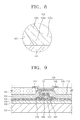
- FIG. 7 illustrates a cross-sectional view of the formation of the intermediate layer 132 using a thermal transfer method.
- a heat source 180 and a donor film 190 for thermal transfer may be arranged above the pixel define layer 120 after the pixel define layer 120 is formed.
- the heat source 180 may include a laser irradiation device.
- the heat source 180 may further include a mask (not shown) and a lens (not shown) to irradiate laser beams to a desired region.
- the donor film 190 may include a base film 191 and a light-to-heat conversion layer 192.
- the intermediate layer 132 which is a transfer layer, may be attached to the bottom surface of the donor film 190.
- the heat source 180 may irradiate laser beams to the top surface of the donor film 190. Then, the intermediate layer 132 as the transfer layer may be detached from the donor film 190 and may be transferred to the first electrode 131. The intermediate layer 132 may be transferred to a desired region of the first electrode 131 using a mask (not shown).
- the intermediate layer 132 when the intermediate layer 132 is transferred using a thermal transfer method, there may be regions in the intermediate layer 132 that may detach from the first electrode 131. In particular, since the intermediate layer 132 may be detached from the first electrode at edges of the opening where it is bent, this phenomenon is referred to as an edge open.
- the edge open may be caused by the step between the first electrode 131 and the pixel define layer 120. Due to the step, the intermediate layer 132 may bend. At the regions where the intermediate layer 132 bends, the intermediate layer 132 may not be properly transferred to the first electrode 131 and may be detached from the first electrode 131.
- the intermediate layer 132 may be prevented from being detached from the first electrode 131 by reducing the step of the intermediate layer 132 when the intermediate layer 132 is formed using a thermal transfer method.
- FIG. 8 illustrates a magnified view of a part A of FIG. 7 .
- the intermediate layer 132 may include a bottom 132a, a bend 132b, and a side 132c.
- the luminescent properties of the organic emissive device 130 may be influenced by the bottom 132a, which is in contact with the first electrode 131, and the bend 132b of the intermediate layer 132.
- the luminescent properties of the organic emissive device 130 may not be sufficient when the intermediate layer 132 is formed using a thermal transfer method, since due to the step between the first electrode 131 and the pixel define layer 120 the intermediate layer 132, particularly the bend 132b of the intermediate layer 132, may often be detached from the first electrode 131.
- the bottom 132a and the bend 132b may not be detached from the first electrode 131 and, thus, may be easily attached thereto as illustrated in FIG. 8 .
- the step between the first electrode 131 and the pixel define layer 120 may be significantly reduced by forming the groove 112 on the insulating layer 110, which in turn may reduce the step of the intermediate layer 132. Therefore, the intermediate layer 132 may be easily transferred to the first electrode 131 and may not have any detached spaces from the first electrode 131.
- the second electrode 133 may be formed on the intermediate layer 132. Materials used to form the intermediate layer 132 and the second electrode 133 have already been described above with reference to FIG. 1 , and thus, detailed description thereof will be omitted.
- the sealing member (not shown) may be formed to face the surface of the substrate 101.
- the sealing member may protect the organic emissive device 130 from external moisture or oxygen, and may be formed of a transparent material.
- the sealing member may be a glass substrate, a plastic substrate, or a multi-layered structure including an organic material and an inorganic material.
- the step between the organic emissive layer and the pixel define layer may be reduced, and thus, the organic emissive layer may be easily formed in the opening and image quality may thereby be improved.
Applications Claiming Priority (1)
| Application Number | Priority Date | Filing Date | Title |
|---|---|---|---|
| KR1020080067829A KR20100007266A (ko) | 2008-07-11 | 2008-07-11 | 유기 발광 표시 장치 및 그 제조 방법 |
Publications (2)
| Publication Number | Publication Date |
|---|---|
| EP2144292A2 true EP2144292A2 (de) | 2010-01-13 |
| EP2144292A3 EP2144292A3 (de) | 2013-05-22 |
Family
ID=40885931
Family Applications (1)
| Application Number | Title | Priority Date | Filing Date |
|---|---|---|---|
| EP09165021.8A Withdrawn EP2144292A3 (de) | 2008-07-11 | 2009-07-09 | Display aus organischen Leuchtdioden und dessen Herstellungsmethode |
Country Status (5)
| Country | Link |
|---|---|
| US (1) | US8164252B2 (de) |
| EP (1) | EP2144292A3 (de) |
| JP (2) | JP2010020311A (de) |
| KR (1) | KR20100007266A (de) |
| CN (1) | CN101626029B (de) |
Cited By (2)
| Publication number | Priority date | Publication date | Assignee | Title |
|---|---|---|---|---|
| CN114207697A (zh) * | 2019-07-29 | 2022-03-18 | Lg伊诺特有限公司 | 显示基板及包括该显示基板的显示装置 |
| US20220102688A1 (en) * | 2019-06-14 | 2022-03-31 | Hewlett-Packard Development Company, L.P. | Organic light emitting transistor devices with shared substrates |
Families Citing this family (22)
| Publication number | Priority date | Publication date | Assignee | Title |
|---|---|---|---|---|
| KR101193184B1 (ko) * | 2009-11-26 | 2012-10-19 | 삼성디스플레이 주식회사 | 유기 발광 디스플레이 장치 및 이를 제조 하는 방법 |
| US8922463B2 (en) * | 2010-04-26 | 2014-12-30 | Samsung Display Co., Ltd. | Organic light-emitting display apparatus |
| KR20120043438A (ko) * | 2010-10-26 | 2012-05-04 | 삼성모바일디스플레이주식회사 | 유기 발광 표시 장치 |
| KR101923172B1 (ko) * | 2011-05-16 | 2018-11-29 | 삼성디스플레이 주식회사 | 유기 발광 표시 장치 및 이의 제조 방법 |
| KR101876540B1 (ko) * | 2011-12-28 | 2018-07-10 | 삼성디스플레이 주식회사 | 가요성 표시 장치 및 가요성 표시 장치의 제조 방법 |
| JP5988624B2 (ja) * | 2012-03-09 | 2016-09-07 | キヤノン株式会社 | 発光装置及びこれを用いた撮像装置、画像形成装置 |
| CN103928497B (zh) * | 2014-04-01 | 2016-07-13 | 京东方科技集团股份有限公司 | Oled显示器件及其制作方法、显示装置 |
| KR20150137214A (ko) * | 2014-05-28 | 2015-12-09 | 삼성디스플레이 주식회사 | 유기발광 디스플레이 장치 및 그 제조방법 |
| KR102360783B1 (ko) | 2014-09-16 | 2022-02-10 | 삼성디스플레이 주식회사 | 디스플레이 장치 |
| KR102284756B1 (ko) | 2014-09-23 | 2021-08-03 | 삼성디스플레이 주식회사 | 디스플레이 장치 |
| CN104659072B (zh) | 2015-03-16 | 2017-07-28 | 京东方科技集团股份有限公司 | 阵列基板和阵列基板制作方法 |
| KR102462423B1 (ko) * | 2015-09-15 | 2022-11-03 | 삼성디스플레이 주식회사 | 유기 발광 표시 장치 및 그 제조 방법 |
| CN105304681B (zh) * | 2015-10-19 | 2019-09-17 | 广东聚华印刷显示技术有限公司 | 含有机/无机混合发光层的电致发光显示器及制备方法 |
| CN105679961A (zh) | 2016-01-26 | 2016-06-15 | 京东方科技集团股份有限公司 | 一种oled封装结构、显示设备及封装方法 |
| KR102591636B1 (ko) * | 2016-03-24 | 2023-10-20 | 삼성디스플레이 주식회사 | 유기발광 디스플레이 장치 |
| CN105826358B (zh) * | 2016-05-24 | 2019-02-05 | 京东方科技集团股份有限公司 | 一种显示基板及其制备方法、显示面板、显示装置 |
| CN108878472B (zh) | 2017-05-12 | 2021-04-06 | 京东方科技集团股份有限公司 | 一种oled显示基板及其制作方法、显示装置 |
| CN107146809A (zh) * | 2017-05-16 | 2017-09-08 | 京东方科技集团股份有限公司 | 阵列基板及其制造方法 |
| US10541380B1 (en) | 2018-08-30 | 2020-01-21 | Samsung Display Co., Ltd. | Display device with substrate comprising an opening and adjacent grooves |
| CN109461760B (zh) * | 2018-09-30 | 2021-06-01 | 云谷(固安)科技有限公司 | 有机发光显示面板与显示装置 |
| KR20200145902A (ko) | 2019-06-19 | 2020-12-31 | 삼성디스플레이 주식회사 | 표시 패널 |
| CN111628105B (zh) * | 2020-06-04 | 2023-05-26 | 京东方科技集团股份有限公司 | 显示面板及其制备方法、显示基板及其制备方法和显示装置 |
Citations (3)
| Publication number | Priority date | Publication date | Assignee | Title |
|---|---|---|---|---|
| US20050285100A1 (en) | 2004-06-28 | 2005-12-29 | Chang-Yong Jeong | Organic light emitting display and method of fabricating the same |
| US20060076887A1 (en) | 2004-10-11 | 2006-04-13 | Tae-Wook Kang | OLED encapsulation structure and method of fabricating the same |
| US20060082293A1 (en) | 2004-10-15 | 2006-04-20 | Tae-Wook Kang | Organic light emitting display |
Family Cites Families (18)
| Publication number | Priority date | Publication date | Assignee | Title |
|---|---|---|---|---|
| KR100656490B1 (ko) * | 2001-11-26 | 2006-12-12 | 삼성에스디아이 주식회사 | 풀칼라 유기전계 발광표시소자 및 그의 제조방법 |
| KR100472502B1 (ko) * | 2001-12-26 | 2005-03-08 | 삼성에스디아이 주식회사 | 유기 전계 발광 표시 장치 |
| AU2003284470A1 (en) * | 2002-12-10 | 2004-06-30 | Semiconductor Energy Laboratory Co., Ltd. | Light-emitting device and its fabricating method |
| JP4702516B2 (ja) * | 2003-05-07 | 2011-06-15 | エルジー エレクトロニクス インコーポレイティド | 有機el素子及びその製造方法 |
| JP4222880B2 (ja) * | 2003-06-02 | 2009-02-12 | 三菱電機株式会社 | 有機電界発光表示装置およびその製造方法 |
| JP2005063838A (ja) * | 2003-08-13 | 2005-03-10 | Toshiba Matsushita Display Technology Co Ltd | 光学デバイス及び有機el表示装置 |
| KR100551046B1 (ko) * | 2003-08-28 | 2006-02-09 | 삼성에스디아이 주식회사 | 유기 이엘 소자 |
| KR20050029426A (ko) * | 2003-09-22 | 2005-03-28 | 삼성에스디아이 주식회사 | 칼라필터층 또는 색변환층을 갖는 풀칼라 유기전계발광소자 |
| JP4453385B2 (ja) * | 2004-02-13 | 2010-04-21 | ソニー株式会社 | 表示装置の製造方法 |
| KR100635066B1 (ko) * | 2004-06-03 | 2006-10-16 | 삼성에스디아이 주식회사 | 유기 전계 발광 표시 장치 및 그의 제조 방법 |
| US7557369B2 (en) * | 2004-07-29 | 2009-07-07 | Samsung Mobile Display Co., Ltd. | Display and method for manufacturing the same |
| KR100700642B1 (ko) * | 2004-12-13 | 2007-03-27 | 삼성에스디아이 주식회사 | 유기전계발광표시소자 및 그 제조방법 |
| KR100647325B1 (ko) * | 2005-04-21 | 2006-11-23 | 삼성전자주식회사 | 저면발광형 유기발광소자 |
| JP2007121994A (ja) * | 2005-09-30 | 2007-05-17 | Epson Imaging Devices Corp | 電気光学装置、及び、電子機器 |
| JP4864520B2 (ja) * | 2006-04-12 | 2012-02-01 | 三菱電機株式会社 | 有機el表示装置および有機el表示装置の製造方法 |
| JP5023599B2 (ja) * | 2006-08-01 | 2012-09-12 | 三菱電機株式会社 | 有機el表示装置 |
| JP2008091223A (ja) * | 2006-10-03 | 2008-04-17 | Sony Corp | 表示装置 |
| JP5063294B2 (ja) * | 2006-11-17 | 2012-10-31 | キヤノン株式会社 | 発光装置及びその製造方法 |
-
2008
- 2008-07-11 KR KR1020080067829A patent/KR20100007266A/ko active Application Filing
-
2009
- 2009-07-09 US US12/458,371 patent/US8164252B2/en active Active
- 2009-07-09 JP JP2009163022A patent/JP2010020311A/ja active Pending
- 2009-07-09 EP EP09165021.8A patent/EP2144292A3/de not_active Withdrawn
- 2009-07-09 CN CN200910151056.6A patent/CN101626029B/zh active Active
-
2013
- 2013-06-12 JP JP2013123665A patent/JP5676689B2/ja active Active
Patent Citations (3)
| Publication number | Priority date | Publication date | Assignee | Title |
|---|---|---|---|---|
| US20050285100A1 (en) | 2004-06-28 | 2005-12-29 | Chang-Yong Jeong | Organic light emitting display and method of fabricating the same |
| US20060076887A1 (en) | 2004-10-11 | 2006-04-13 | Tae-Wook Kang | OLED encapsulation structure and method of fabricating the same |
| US20060082293A1 (en) | 2004-10-15 | 2006-04-20 | Tae-Wook Kang | Organic light emitting display |
Cited By (3)
| Publication number | Priority date | Publication date | Assignee | Title |
|---|---|---|---|---|
| US20220102688A1 (en) * | 2019-06-14 | 2022-03-31 | Hewlett-Packard Development Company, L.P. | Organic light emitting transistor devices with shared substrates |
| CN114207697A (zh) * | 2019-07-29 | 2022-03-18 | Lg伊诺特有限公司 | 显示基板及包括该显示基板的显示装置 |
| CN114207697B (zh) * | 2019-07-29 | 2024-03-08 | Lg伊诺特有限公司 | 显示基板及包括该显示基板的显示装置 |
Also Published As
| Publication number | Publication date |
|---|---|
| KR20100007266A (ko) | 2010-01-22 |
| US8164252B2 (en) | 2012-04-24 |
| US20100007271A1 (en) | 2010-01-14 |
| CN101626029B (zh) | 2015-02-18 |
| CN101626029A (zh) | 2010-01-13 |
| JP2013175487A (ja) | 2013-09-05 |
| JP5676689B2 (ja) | 2015-02-25 |
| EP2144292A3 (de) | 2013-05-22 |
| JP2010020311A (ja) | 2010-01-28 |
Similar Documents
| Publication | Publication Date | Title |
|---|---|---|
| US8164252B2 (en) | Organic light emitting diode display apparatus and method of manufacturing the same | |
| US8461591B2 (en) | Organic light emitting display apparatus and method of manufacturing the same | |
| US9343521B2 (en) | Organic light-emitting display apparatus and method of manufactuing the same | |
| US8395160B2 (en) | Organic light emitting display apparatus and method of manufacturing the same | |
| US8643019B2 (en) | Organic light emitting display device and manufacturing method for the same | |
| JP6081688B2 (ja) | 有機発光表示装置 | |
| US20110248297A1 (en) | Light-emitting apparatus and production method thereof | |
| US9331304B2 (en) | Organic light-emitting display device and method of manufacturing the same | |
| US8174003B2 (en) | Organic light emitting display apparatus and method of manufacturing same | |
| US10431762B2 (en) | Display device and manufacturing method thereof | |
| KR100932935B1 (ko) | 유기 발광 소자 및 이를 포함하는 유기 발광 표시 장치 | |
| US8888547B2 (en) | Organic light-emitting display apparatus and method of manufacturing the same | |
| US8227845B2 (en) | Organic light emitting display | |
| JP2010287634A (ja) | トランジスタを有するトランジスタ基板及びトランジスタを有するトランジスタ基板の製造方法 | |
| KR101753773B1 (ko) | 유기 발광 표시 장치 및 그 제조 방법 | |
| US8349416B2 (en) | Donor film and method of manufacturing organic light emitting device using same | |
| KR100927584B1 (ko) | 유기 발광 표시 장치 및 그 제조 방법 | |
| KR20160047450A (ko) | 유기 발광 표시 장치 및 그 제조 방법 | |
| KR100795815B1 (ko) | 유기 발광 표시 장치 | |
| KR20150058131A (ko) | 유기 발광 표시 장치 및 그 제조 방법 |
Legal Events
| Date | Code | Title | Description |
|---|---|---|---|
| PUAI | Public reference made under article 153(3) epc to a published international application that has entered the european phase |
Free format text: ORIGINAL CODE: 0009012 |
|
| 17P | Request for examination filed |
Effective date: 20090709 |
|
| AK | Designated contracting states |
Kind code of ref document: A2 Designated state(s): AT BE BG CH CY CZ DE DK EE ES FI FR GB GR HR HU IE IS IT LI LT LU LV MC MK MT NL NO PL PT RO SE SI SK SM TR |
|
| RAP1 | Party data changed (applicant data changed or rights of an application transferred) |
Owner name: SAMSUNG DISPLAY CO., LTD. |
|
| PUAL | Search report despatched |
Free format text: ORIGINAL CODE: 0009013 |
|
| AK | Designated contracting states |
Kind code of ref document: A3 Designated state(s): AT BE BG CH CY CZ DE DK EE ES FI FR GB GR HR HU IE IS IT LI LT LU LV MC MK MT NL NO PL PT RO SE SI SK SM TR |
|
| AX | Request for extension of the european patent |
Extension state: AL BA RS |
|
| RIC1 | Information provided on ipc code assigned before grant |
Ipc: H01L 27/32 20060101AFI20130416BHEP Ipc: H01L 51/00 20060101ALI20130416BHEP |
|
| 17Q | First examination report despatched |
Effective date: 20140429 |
|
| RAP1 | Party data changed (applicant data changed or rights of an application transferred) |
Owner name: SAMSUNG DISPLAY CO., LTD. |
|
| STAA | Information on the status of an ep patent application or granted ep patent |
Free format text: STATUS: THE APPLICATION IS DEEMED TO BE WITHDRAWN |
|
| 18D | Application deemed to be withdrawn |
Effective date: 20180201 |