EP2141747B2 - Module de cellule solaire - Google Patents
Module de cellule solaire Download PDFInfo
- Publication number
- EP2141747B2 EP2141747B2 EP09251721.8A EP09251721A EP2141747B2 EP 2141747 B2 EP2141747 B2 EP 2141747B2 EP 09251721 A EP09251721 A EP 09251721A EP 2141747 B2 EP2141747 B2 EP 2141747B2
- Authority
- EP
- European Patent Office
- Prior art keywords
- solar cell
- light receiving
- receiving surface
- reflecting plate
- surface side
- Prior art date
- Legal status (The legal status is an assumption and is not a legal conclusion. Google has not performed a legal analysis and makes no representation as to the accuracy of the status listed.)
- Active
Links
- 238000006243 chemical reaction Methods 0.000 claims description 19
- 238000000034 method Methods 0.000 claims description 7
- 239000000853 adhesive Substances 0.000 claims description 5
- 230000001070 adhesive effect Effects 0.000 claims description 5
- 238000009413 insulation Methods 0.000 claims description 5
- 239000000969 carrier Substances 0.000 claims description 4
- 238000001579 optical reflectometry Methods 0.000 claims description 4
- 239000007769 metal material Substances 0.000 claims description 2
- 230000005855 radiation Effects 0.000 description 7
- 239000011347 resin Substances 0.000 description 7
- 229920005989 resin Polymers 0.000 description 7
- 229910052751 metal Inorganic materials 0.000 description 6
- 239000002184 metal Substances 0.000 description 6
- 239000004020 conductor Substances 0.000 description 5
- 238000007789 sealing Methods 0.000 description 5
- 239000004065 semiconductor Substances 0.000 description 5
- 238000004519 manufacturing process Methods 0.000 description 4
- 239000000463 material Substances 0.000 description 4
- PXHVJJICTQNCMI-UHFFFAOYSA-N Nickel Chemical compound [Ni] PXHVJJICTQNCMI-UHFFFAOYSA-N 0.000 description 2
- ATJFFYVFTNAWJD-UHFFFAOYSA-N Tin Chemical compound [Sn] ATJFFYVFTNAWJD-UHFFFAOYSA-N 0.000 description 2
- 239000000919 ceramic Substances 0.000 description 2
- 238000009792 diffusion process Methods 0.000 description 2
- 230000000694 effects Effects 0.000 description 2
- 239000011888 foil Substances 0.000 description 2
- 230000003287 optical effect Effects 0.000 description 2
- 238000007747 plating Methods 0.000 description 2
- 229920000139 polyethylene terephthalate Polymers 0.000 description 2
- 239000005020 polyethylene terephthalate Substances 0.000 description 2
- 229910052718 tin Inorganic materials 0.000 description 2
- RYGMFSIKBFXOCR-UHFFFAOYSA-N Copper Chemical compound [Cu] RYGMFSIKBFXOCR-UHFFFAOYSA-N 0.000 description 1
- 239000004593 Epoxy Substances 0.000 description 1
- JOYRKODLDBILNP-UHFFFAOYSA-N Ethyl urethane Chemical compound CCOC(N)=O JOYRKODLDBILNP-UHFFFAOYSA-N 0.000 description 1
- 229910001218 Gallium arsenide Inorganic materials 0.000 description 1
- BQCADISMDOOEFD-UHFFFAOYSA-N Silver Chemical compound [Ag] BQCADISMDOOEFD-UHFFFAOYSA-N 0.000 description 1
- NIXOWILDQLNWCW-UHFFFAOYSA-N acrylic acid group Chemical group C(C=C)(=O)O NIXOWILDQLNWCW-UHFFFAOYSA-N 0.000 description 1
- 229910045601 alloy Inorganic materials 0.000 description 1
- 239000000956 alloy Substances 0.000 description 1
- 229910052782 aluminium Inorganic materials 0.000 description 1
- XAGFODPZIPBFFR-UHFFFAOYSA-N aluminium Chemical compound [Al] XAGFODPZIPBFFR-UHFFFAOYSA-N 0.000 description 1
- 230000015572 biosynthetic process Effects 0.000 description 1
- 150000001875 compounds Chemical class 0.000 description 1
- 239000000470 constituent Substances 0.000 description 1
- 229910052802 copper Inorganic materials 0.000 description 1
- 239000010949 copper Substances 0.000 description 1
- 230000005611 electricity Effects 0.000 description 1
- 239000011521 glass Substances 0.000 description 1
- PCHJSUWPFVWCPO-UHFFFAOYSA-N gold Chemical compound [Au] PCHJSUWPFVWCPO-UHFFFAOYSA-N 0.000 description 1
- 229910052737 gold Inorganic materials 0.000 description 1
- 239000010931 gold Substances 0.000 description 1
- 239000011810 insulating material Substances 0.000 description 1
- 238000002955 isolation Methods 0.000 description 1
- 150000002739 metals Chemical class 0.000 description 1
- 229910021421 monocrystalline silicon Inorganic materials 0.000 description 1
- 229910052759 nickel Inorganic materials 0.000 description 1
- 239000004033 plastic Substances 0.000 description 1
- 229920003023 plastic Polymers 0.000 description 1
- 229910021420 polycrystalline silicon Inorganic materials 0.000 description 1
- -1 polyethylene terephthalate Polymers 0.000 description 1
- 229920001296 polysiloxane Polymers 0.000 description 1
- 229910052709 silver Inorganic materials 0.000 description 1
- 239000004332 silver Substances 0.000 description 1
- 229910000679 solder Inorganic materials 0.000 description 1
- 239000011135 tin Substances 0.000 description 1
Images


Classifications
-
- H—ELECTRICITY
- H01—ELECTRIC ELEMENTS
- H01L—SEMICONDUCTOR DEVICES NOT COVERED BY CLASS H10
- H01L31/00—Semiconductor devices sensitive to infrared radiation, light, electromagnetic radiation of shorter wavelength or corpuscular radiation and specially adapted either for the conversion of the energy of such radiation into electrical energy or for the control of electrical energy by such radiation; Processes or apparatus specially adapted for the manufacture or treatment thereof or of parts thereof; Details thereof
- H01L31/04—Semiconductor devices sensitive to infrared radiation, light, electromagnetic radiation of shorter wavelength or corpuscular radiation and specially adapted either for the conversion of the energy of such radiation into electrical energy or for the control of electrical energy by such radiation; Processes or apparatus specially adapted for the manufacture or treatment thereof or of parts thereof; Details thereof adapted as photovoltaic [PV] conversion devices
- H01L31/042—PV modules or arrays of single PV cells
- H01L31/05—Electrical interconnection means between PV cells inside the PV module, e.g. series connection of PV cells
- H01L31/0504—Electrical interconnection means between PV cells inside the PV module, e.g. series connection of PV cells specially adapted for series or parallel connection of solar cells in a module
-
- H—ELECTRICITY
- H01—ELECTRIC ELEMENTS
- H01L—SEMICONDUCTOR DEVICES NOT COVERED BY CLASS H10
- H01L31/00—Semiconductor devices sensitive to infrared radiation, light, electromagnetic radiation of shorter wavelength or corpuscular radiation and specially adapted either for the conversion of the energy of such radiation into electrical energy or for the control of electrical energy by such radiation; Processes or apparatus specially adapted for the manufacture or treatment thereof or of parts thereof; Details thereof
- H01L31/04—Semiconductor devices sensitive to infrared radiation, light, electromagnetic radiation of shorter wavelength or corpuscular radiation and specially adapted either for the conversion of the energy of such radiation into electrical energy or for the control of electrical energy by such radiation; Processes or apparatus specially adapted for the manufacture or treatment thereof or of parts thereof; Details thereof adapted as photovoltaic [PV] conversion devices
- H01L31/042—PV modules or arrays of single PV cells
- H01L31/048—Encapsulation of modules
-
- H—ELECTRICITY
- H01—ELECTRIC ELEMENTS
- H01L—SEMICONDUCTOR DEVICES NOT COVERED BY CLASS H10
- H01L31/00—Semiconductor devices sensitive to infrared radiation, light, electromagnetic radiation of shorter wavelength or corpuscular radiation and specially adapted either for the conversion of the energy of such radiation into electrical energy or for the control of electrical energy by such radiation; Processes or apparatus specially adapted for the manufacture or treatment thereof or of parts thereof; Details thereof
- H01L31/04—Semiconductor devices sensitive to infrared radiation, light, electromagnetic radiation of shorter wavelength or corpuscular radiation and specially adapted either for the conversion of the energy of such radiation into electrical energy or for the control of electrical energy by such radiation; Processes or apparatus specially adapted for the manufacture or treatment thereof or of parts thereof; Details thereof adapted as photovoltaic [PV] conversion devices
- H01L31/054—Optical elements directly associated or integrated with the PV cell, e.g. light-reflecting means or light-concentrating means
- H01L31/0547—Optical elements directly associated or integrated with the PV cell, e.g. light-reflecting means or light-concentrating means comprising light concentrating means of the reflecting type, e.g. parabolic mirrors, concentrators using total internal reflection
-
- Y—GENERAL TAGGING OF NEW TECHNOLOGICAL DEVELOPMENTS; GENERAL TAGGING OF CROSS-SECTIONAL TECHNOLOGIES SPANNING OVER SEVERAL SECTIONS OF THE IPC; TECHNICAL SUBJECTS COVERED BY FORMER USPC CROSS-REFERENCE ART COLLECTIONS [XRACs] AND DIGESTS
- Y02—TECHNOLOGIES OR APPLICATIONS FOR MITIGATION OR ADAPTATION AGAINST CLIMATE CHANGE
- Y02E—REDUCTION OF GREENHOUSE GAS [GHG] EMISSIONS, RELATED TO ENERGY GENERATION, TRANSMISSION OR DISTRIBUTION
- Y02E10/00—Energy generation through renewable energy sources
- Y02E10/50—Photovoltaic [PV] energy
- Y02E10/52—PV systems with concentrators
Definitions
- the present invention relates to a solar cell module including solar cells connected to each other by wiring members.
- a Solar cell directly converts clean and unlimitedly supplied sunlight into electricity.
- the solar cells are expected as a new energy source.
- the output of a single solar cell is about several watts. For this reason, in order to use such a solar cell as a power source for a house, a building, or the like, a solar cell module in which solar cells are connected to each other to increase the output is used.
- the solar cell module includes solar cells which are sealed with a sealing member between a light receiving surface side protection member and a back surface side protection member.
- the solar cells are arrayed in an array direction and electrically connected to each other by wiring members.
- each of the wiring members is connected to a light receiving surface of one solar cell and to a back surface of a different solar cell adjacent to the one solar cell.
- the above-described wiring member is usually formed by cutting a long metal wire to a predetermined length, the metal wire having asperities formed entirely in one-side surface.
- a problem arises when such a wiring member is connected to the light receiving surface of the one solar cell and to the back surface of the other solar cell. That is, the adhesion between the back surface of the other solar cell and the wiring member is lowered because the asperities are formed in the one-side surface of the wiring member facing the back surface of the other solar cell.
- WO99/09601 discloses a solar cell assembly for focusing incident radiation on a solar cell.
- the assembly comprises a reflective member having first and second opposite surfaces.
- the first surface is transparent to allow incident radiation to pass into the reflective member.
- the second surface has a plurality of reflective portions positioned to receive the radiation and reflect and focus the radiation toward the first surface.
- the radiation strikes the first surface at an angle greater than a critical angle of the first surface and is reflected and focused back toward the second surface.
- the assembly further comprises a solar cell positioned at least proximate to the reflective member to receive the radiation reflected and focused from the first surface of the reflective member and generate electric current from the radiation.
- US 2005/0016580 A1 discloses a solar battery module wherein a light diffusion section for diffusely reflecting a light or a light diffusion section of a white colour is arranged in an invalid region of each solar cell.
- a preferred aim of the present invention is to provide a solar cell module having a reduced optical loss caused by a surface of a wiring member while maintaining excellent adhesion between the wiring member and a solar cell.
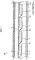
- FIG. 1 is a side view of the solar cell module 100 according to the first embodiment.
- the solar cell module 100 includes a solar cell string 1, a light receiving surface side protection member 2, a back surface side protection member 3, and a sealing member 4.
- the solar cell string 1 is sealed between the light receiving surface side protection member 2 and the back surface side protection member 3 with the sealing member 4.
- the solar cell string 1 includes solar cells 10 (solar cells 10a to 10c), wiring members 11, and a reflecting plate 12.
- the solar cells 10 are electrically connected to each other by the wiring members 11.
- the reflecting plate 12 is disposed between the light receiving surface side protection member 2 and the solar cells 10. Specifically, the reflecting plate 12 is disposed on the wiring members 11. The configuration of the solar cell string 1 will be described later in detail.
- Each of the solar cells 10 has a light receiving surface that faces the light receiving surface side protection member 2, and a back surface that is provided on a side opposite to the light receiving surface and faces the back surface side protection member 3.
- the solar cells 10 are arrayed in an array direction H. The configuration of each of the solar cells 10 will be described later in detail.
- the light receiving surface side protection member 2 is disposed on a light receiving surface side of each of the solar cells 10, and protects the front surface of the solar cell module 100.
- a translucent and water-shielding glass, a translucent plastic, or the like may be used for the light receiving surface side protection member 2.
- the back surface side protection member 3 is disposed on a back surface side of each of the solar cells 10, and protects the back surface of the solar cell module 100.
- a resin film made of polyethylene terephthalate (PET) or the like, or a stacked film having such a structure that a metal foil such as an Al foil or the like is sandwiched by resin films may be used, for example.
- the sealing member 4 seals the solar cell string 1 between the light receiving surface side protection member 2 and the back surface side protection member 3.
- a translucent resin such as EVA, EEA, PVB, silicone, urethane, acrylic, epoxy, or the like may be used.
- an Al frame (unillustrated) may be attached to the periphery of the solar cell module 100 having the above-described configuration.
- Fig. 2A is a plan view of the solar cell 10 viewed from the light receiving surface side.
- Fig. 2B is a plan view of the solar cell 10 viewed from the back surface side.
- the solar cell 10 includes a photoelectric conversion part 20, thin line-shaped electrodes 30, and connecting electrodes 40.
- the thin line-shaped electrodes 30 and connecting electrodes 40 are formed in a comb shape similarly on both the light receiving surface and the back surface of the solar cell 10.
- the photoelectric conversion part 20 generates photo-generated carriers by receiving light.
- the photo-generated carriers are holes and electrons generated when the photoelectric conversion part 20 absorbs solar light.
- the photoelectric conversion part 20 is provided inside with a semiconductor junction such as a pn junction, pin junction, or the like.
- the photoelectric conversion part 20 can be formed by using a general semiconductor material. Examples of such a semiconductor material include: a crystalline semiconductor material, such as a monocrystalline Si or a polycrystalline Si; a compound semiconductor material, such as GaAs or InP; and the like.
- the thin line-shaped electrodes 30 are collecting electrodes collecting carriers from the photoelectric conversion part 20. Each of the thin line-shaped electrodes 30 is formed on the photoelectric conversion part 20 so as to extend in an orthogonal direction K approximately orthogonal to the array direction H. Each of the thin line-shaped electrodes 30 can be made of, for example, a resin conductive paste, a sintered conductive paste (i.e., ceramic paste), or the like. Note that the size and the number of the thin line-shaped electrodes 30 can be set as appropriate in consideration of the size and the properties of the photoelectric conversion part 20. For example, in a case where the photoelectric conversion part 20 has a size of approximately 100 mm square, approximately 50 thin line-shaped electrodes 30 can be formed. In addition, on the back surface of the solar cell 10, a collecting electrode covering the entire back surface may be formed instead of the thin line-shaped electrodes 30.
- the connecting electrodes 40 are connected to the wiring members 11.
- the connecting electrodes 40 are formed on the photoelectric conversion part 20 so as to extend in the array direction H.
- the connecting electrodes 40 can be made of a resin conductive paste, a sintered conductive paste (ceramic paste), or the like. Note that the size and the number of the connecting electrodes 40 can be set as appropriate in consideration of the size and the properties of the photoelectric conversion part 20. For example, in a case where the photoelectric conversion part 20 has a size of approximately 100 mm square, two connecting electrodes 40 each having a width of approximately 1.5 mm can be formed.
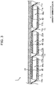
- Fig. 3 is an enlarged side view of the solar cell string 1.
- Fig. 4 is a plan view of the solar cell string 1 viewed from the light receiving surface side.
- each of the wiring members 11 electrically connects one solar cell 10 and a different solar cell 10 adjacent to the one solar cell 10.
- the wiring members 11 extend in the array direction H and are connected to the connecting electrode 40 formed on the light receiving surface of the one solar cell 10 and to the connecting electrode 40 formed on the back surface of the different solar cell 10.
- each of the wiring members 11 has: a connecting portion 11a, a connecting portion 11b, and a communicating portion 11c.
- the connecting portion 11a is a portion of the wiring member 11 that is connected to the light receiving surface of the one solar cell 10.
- the connecting portion 11b is a portion of the wiring member 11 that is connected to the back surface of the different solar cell 10.
- the communicating portion 11c is a portion of the wiring member 11 that communicates with the connecting portion 11a and the connecting portion 11b.
- the light receiving surface of the solar cell 10 has one polarity whereas the back surface thereof has the other polarity.
- the one solar cell 10 and the different solar cell 10 are electrically connected to each other in series by the wiring members 11.
- Each of the wiring members 11 is made of a low resistance element and a conductive material covering a surface of the low resistance element.
- a low resistance element a thin plate or a twisted wire made of copper, silver, gold, tin, nickel, aluminum, an alloy of any of these metals, or the like may be used.
- a conductive material lead-free solder plating, tin plating, or the like may be used.
- the reflecting plate 12 is disposed over connecting portions 11a of each of the wiring members 11. Note that, the reflecting plate 12 is bonded to the connecting portions 11a by use of a resin adhesive or the like, although such bonding is not illustrated in the drawing.
- the reflecting plate 12 is disposed over the solar cells 10 so as to extend in the array direction H, in a plan view seen from the light receiving surface side of the solar cell string 1.
- the reflecting plate 12 is made of a conductive metal material.
- a surface of the reflecting plate 12 that faces the connecting portions 11a provides electrical isolation. This structure suppresses occurrences of electrical short circuits between the solar cells 10.
- the surface of the reflecting plate 12 that faces the connecting portions 11a is subjected to an insulation process, or the reflecting plate 12 is bonded to the connecting portions 11a by use of an insulative adhesive so that the reflecting plate 12 can be electrically separated from the connecting portions 11a.
- a surface (a top surface) of the reflecting plate 12 that faces the light receiving surface side protection member 2 has light reflectivity.
- multiple asperities are formed entirely in the top surface of the reflecting plate 12. This structure allows reflection (including scattering) of incident light toward each of the reflecting plate 12 (toward the wiring members 11) by the surfaces of the respective asperities. The light reflected by the surfaces of the respective asperities is reflected again at the interface between the light receiving surface side protection member 2 and the atmosphere, and then enters the photoelectric conversion part 20.
- the base angles of each of the convex portions of the asperities formed in the top surface of the reflecting plate 12 is preferably determined so that light reflected by the surface of the convex portion would be totally reflected at the interface between the light receiving surface side protection member 2 and the atmosphere.
- the solar cell module 100 includes: the solar cells 10; the wiring members 11 electrically connecting the solar cells 10 to each other; and the reflecting plate 12 disposed between the light receiving surface side protection member 2 and the solar cells 10.
- the wiring members 11 have the connecting portions 11a connected to the light receiving surface of each of the solar cells 10.
- the reflecting plate 12 is disposed over the connecting portions 11a of the wiring members 11.
- the top surface of the reflecting plate 12 has light reflectivity.
- the reflecting plate 12 can be disposed on the solar cells 10 with the resin adhesive interposed therebetween, the solar cells 10 connected to each other by the wiring members 11.
- the reflecting plate 12 can be easily attached in the manufacturing process of the solar cell module 100.
- the surface of the reflecting plate 12 that faces the connecting portion 11a and the connecting portion 11b of the respective wiring members 11 has insulating properties, thereby suppressing occurrences of short circuits between the solar cells 10 even when the reflecting plate 12 is made of a conductive material.
- the occurrences of short circuits between the solar cells 10 can be suppressed by performing an insulation process on the surface of the reflecting plate 12 that faces the connecting portions 11a, or by bonding the reflecting plate 12 and the connecting portions 11a together by use of an insulative adhesive.
- the reflecting plate 12 has multiple conductive portions disposed respectively on connecting portions 11a of the wiring members 11, and multiple insulating portions each communicating with a pair of adjacent conductive portions.
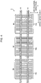
- Fig. 5 is an enlarged side view of the solar cell string 1.
- Fig. 6 is a plan view of the solar cell string 1 viewed from the light receiving surface side.
- the reflecting plate 12 has conductive portions 12a disposed respectively on connecting portions 11a of the wiring members 11, and insulating portions 12b communicating with a pair of adjacent conductive portions 12a.
- Each of the conductive portions 12a is made of a conductive material such as metal. No insulation process is performed on the surfaces of the reflecting plate 12 according to this non-claimed example, and thus the conductive portions 12a and the respective connecting portions 11a are electrically connected to each other.
- Each insulating portion 12b is made of a known insulating material, and electrically separates the pair of the adjacent conductive portions 12a. Note that the conductive portions 12a and the insulating portions 12b are formed integrally. In addition, a surface of the conductive portions 12a and the insulating portions 12b that face a light receiving surface side protection member 2 has light reflectivity.
- the reflecting plate 12 according to the first non-claimed example has the conductive portions 12a and the insulating portions 12b each communicating with the pair of the adjacent conductive portions 12a.
- the conductive portions 12a are electrically connected to the connecting portions 11a, and thus function as part of the wiring members 11, respectively. It is therefore possible to reduce the inner electrical resistance of the wiring members 11.
- the reflecting plate 12 can be easily disposed in the manufacturing process of the solar cell module 100.
- the wiring members 11 are each connected to light receiving surfaces of a pair of adjacent solar cells 10, or connected to back surfaces of the solar cells 10.
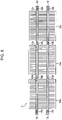
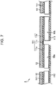
- Fig. 7 is an enlarged side view of a solar cell string 1 according to the second non-claimed example.
- the wiring members 11 include: wiring members 111 each disposed on the light receiving surface sides of each of the solar cells 10; and wiring members 112 each disposed on the back surface sides of each of the solar cells 10.
- each of the wiring members 111 has: a pair of connecting portion 11a connected to a pair of the light receiving surface of the adjacent solar cells 10 (the solar cell 10a and the solar cell 10b); and a communicating portion 11c communicating with the pair of connecting portion 11a.
- the pair of connecting portion 11a and the communicating portion 11c are integrally formed.
- Each of the wiring members 112 is connected to a pair of the back surface of the adjacent solar cells 10.
- the polarity of the light receiving surface of the solar cell 10a is different from that of the light receiving surface of the solar cell 10b.
- the solar cell 10a is electrically connected to the solar cell 10b in series by one of the wiring members 111.
- each of reflecting plates 12 is disposed over the pair of the connecting portion 11a of the wiring members 111.
- each of the reflecting plates 12 according to the second non-claimed example is disposed on each of the wiring members 111 in an array direction.
- each of the reflecting plates 12 is made of a conductive material, such as metal, and electrically connected to each of the wiring members 111.
- one wiring member 11 may connect the solar cell 10a and the solar cell 10b in parallel, connect the solar cell 10c and the solar cell 10d in parallel, and connect the parallel-connected solar cells 10a and 10b and the parallel-connected solar cells 10c and 10d in series.
- each of the wiring members 11 has: a connecting portion 11a connected to the light receiving surfaces of the solar cell 10a and the solar cell 10b; a connecting portion 11b connected the back surfaces of the solar cell 10c and the solar cell 10d; and a communicating portion 11c communicating with the connecting portion 11a and the connecting portion 11b.
- the reflecting plate 12 is disposed over the connecting portions 11a of each of the wiring members 11.
- the reflecting plate 12 may have conductive portions 12a disposed respectively on the connecting portions 11a, and insulating portions 12b each communicating with a pair of the adjacent conductive portions 12a.
- the reflecting plate 12 is disposed on the connecting portions 11a in the above-described embodiment. However, if the solar cells 10 are bifacial-type solar cells, the reflecting plate 12 may be disposed over the connecting portions 11b as well. In other words, the reflecting plate 12 may also be disposed between the back surface side protection member 3 and the solar cells 10.
- the thin line-shaped electrodes 30 and the connecting electrodes 40 are formed in the comb shape, but the configurations of the thin line-shaped electrodes 30 and the connecting electrodes 40 are not limited to this.
- the wiring members 11 may be connected directly to the light receiving surfaces and the back surfaces of each of the solar cells 10 without forming the connecting electrodes 40 on the light receiving surfaces and the back surfaces.
- the number of the solar cells 10 is not limited.
Claims (1)
- Module de cellules solaires (100) comprenant :une pluralité de cellules solaires (10, 10a-10d) comprenant des première à troisième cellules solaires (10a-10c) qui sont disposées en réseau dans une direction de réseau (H) et qui sont scellées entre un élément de protection côté surface de réception de lumière (2) et un élément de protection côté surface arrière (3), et dont chacun présente une surface de réception de lumière et une surface arrière disposée sur un côté opposé à la surface de réception de lumière, et dont chacune comprend une partie de conversion photoélectrique (20) et des électrodes en forme de ligne mince (30) sur la surface de réception de lumière, dans lesquelles les électrodes en forme de ligne mince (30) sont des électrodes de collecte qui collectent des porteuses provenant de la partie de conversion photoélectrique (20), et chacune des électrodes en forme de ligne mince (30) est formée sur la partie de conversion photoélectrique (20) de manière à s'étendre dans une direction orthogonale (K) à la direction de réseau (H) ;un premier élément de câblage (11) connecté à la surface de réception de lumière de la première cellule solaire (10a) et à la surface arrière de la deuxième cellule solaire (10b) ;un second élément de câblage (11) connecté à la surface de réception de lumière de la deuxième cellule solaire (10b) et à la surface arrière de la troisième cellule solaire (10c) ; etune plaque réfléchissante (12) est disposée dans la direction de réseau (H) entre l'élément de protection côté surface de réception de lumière (2) et les première à troisième cellules solaires (10a-10c), et sur le premier élément de câblage (11) et le second élément de câblage (11) ;dans lequel :
le premier élément de câblage (11) présente une première partie de connexion (11a) disposée dans la direction de réseau (H) et connectée à la surface de réception de lumière de la première cellule solaire (10a),le second élément de câblage (11) présente une seconde partie de connexion (11a) disposée dans la direction de réseau (H) et connectée à la surface de réception de lumière de la deuxième cellule solaire (10b),la plaque réfléchissante (12) est disposée sur les première et seconde parties de connexion (11a),de multiples aspérités présentant une réflectivité lumineuse sont formées entièrement dans une surface de la plaque réfléchissante (12) qui fait face à l'élément de protection côté surface de réception de lumière (2), de telle sorte que de la lumière incidente vers chacun des premier et second éléments de câblage (11) est réfléchie séquentiellement par la plaque réfléchissante (12) et l'élément de protection côté surface de réception de lumière (2), puis guidée vers la partie de conversion photoélectrique (20),la plaque réfléchissante (12) est réalisée en un matériau métallique conducteur, etune surface de la plaque réfléchissante (12) qui fait face aux première et seconde parties de connexion (11a) est soumise à un processus d'isolation, ou la plaque réfléchissante (12) est liée aux première et seconde parties de connexion (11a) à l'aide d'un adhésif isolant.
Applications Claiming Priority (1)
| Application Number | Priority Date | Filing Date | Title |
|---|---|---|---|
| JP2008175972A JP5436805B2 (ja) | 2008-07-04 | 2008-07-04 | 太陽電池モジュール |
Publications (4)
| Publication Number | Publication Date |
|---|---|
| EP2141747A2 EP2141747A2 (fr) | 2010-01-06 |
| EP2141747A3 EP2141747A3 (fr) | 2012-02-29 |
| EP2141747B1 EP2141747B1 (fr) | 2018-10-17 |
| EP2141747B2 true EP2141747B2 (fr) | 2022-11-16 |
Family
ID=41258430
Family Applications (1)
| Application Number | Title | Priority Date | Filing Date |
|---|---|---|---|
| EP09251721.8A Active EP2141747B2 (fr) | 2008-07-04 | 2009-07-03 | Module de cellule solaire |
Country Status (4)
| Country | Link |
|---|---|
| US (1) | US20100000595A1 (fr) |
| EP (1) | EP2141747B2 (fr) |
| JP (1) | JP5436805B2 (fr) |
| ES (1) | ES2705200T5 (fr) |
Families Citing this family (9)
| Publication number | Priority date | Publication date | Assignee | Title |
|---|---|---|---|---|
| JP5436805B2 (ja) | 2008-07-04 | 2014-03-05 | 三洋電機株式会社 | 太陽電池モジュール |
| US9514466B2 (en) * | 2009-11-16 | 2016-12-06 | Yahoo! Inc. | Collecting and presenting data including links from communications sent to or from a user |
| JP2011249736A (ja) * | 2010-05-31 | 2011-12-08 | Sanyo Electric Co Ltd | 太陽電池モジュールの製造方法 |
| AT509905B1 (de) | 2010-06-14 | 2013-10-15 | Stojec Mario Paul | Photovoltaik-modul |
| WO2012012136A1 (fr) * | 2010-06-30 | 2012-01-26 | First Solar, Inc | Cible de pulvérisation cathodique en stannate de cadmium |
| KR20130083546A (ko) * | 2012-01-13 | 2013-07-23 | 엘지전자 주식회사 | 태양전지 모듈 |
| CN110246918A (zh) * | 2012-03-27 | 2019-09-17 | 3M创新有限公司 | 包括光定向介质的光伏组件及其制备方法 |
| JP2016525707A (ja) * | 2013-07-09 | 2016-08-25 | スリーエム イノベイティブ プロパティズ カンパニー | ソーラーモジュールにおける使用のための円形微細構造を持つ反射フィルム |
| EP3362744A4 (fr) | 2015-10-12 | 2019-06-12 | 3M Innovative Properties Company | Film de redirection de lumière utile avec des modules solaires |
Citations (12)
| Publication number | Priority date | Publication date | Assignee | Title |
|---|---|---|---|---|
| US5011544A (en) † | 1989-09-08 | 1991-04-30 | Solarex Corporation | Solar panel with interconnects and masking structure, and method |
| DE4128766C2 (de) † | 1991-08-29 | 1995-07-20 | Flachglas Ag | Solarmodul sowie Verfahren zu dessen Herstellung |
| JPH1093125A (ja) † | 1996-09-13 | 1998-04-10 | Sanyo Electric Co Ltd | 太陽電池モジュール |
| US5994641A (en) † | 1998-04-24 | 1999-11-30 | Ase Americas, Inc. | Solar module having reflector between cells |
| EP1172864A1 (fr) † | 2000-07-11 | 2002-01-16 | SANYO ELECTRIC Co., Ltd. | Module de cellules de solaires |
| US20050199279A1 (en) † | 2004-01-29 | 2005-09-15 | Sanyo Electric Co., Ltd. | Solar cell module |
| US20050241692A1 (en) † | 2002-08-29 | 2005-11-03 | Rubin Leonid B | Electrode for photovoltaic cells, photovoltaic cell and photovoltaic module |
| US20060107991A1 (en) † | 2004-11-24 | 2006-05-25 | Sanyo Electric Co., Ltd. | Solar cell module |
| JP2007201331A (ja) † | 2006-01-30 | 2007-08-09 | Sanyo Electric Co Ltd | 光起電力モジュール |
| EP1852917A2 (fr) † | 2006-05-03 | 2007-11-07 | Palo Alto Research Institute Incorporated | Cellule biface avec métallisation du quadrillage extrudé |
| DE102006021804A1 (de) † | 2006-05-09 | 2007-11-15 | International Solar Energy Research Center Konstanz E.V. | Solarzellenmodul sowie Verfahren zur Herstellung von Solarzellenmodulen |
| DE102008004771A1 (de) † | 2007-09-27 | 2009-04-16 | Leonhard Kurz Stiftung & Co. Kg | Solarzelle |
Family Cites Families (14)
| Publication number | Priority date | Publication date | Assignee | Title |
|---|---|---|---|---|
| NL1005926C2 (nl) * | 1997-04-29 | 1998-11-02 | Stichting Energie | Zonnepaneel met in serie geschakelde fotovoltaïsche eenheden. |
| US6008449A (en) | 1997-08-19 | 1999-12-28 | Cole; Eric D. | Reflective concentrating solar cell assembly |
| JP3679611B2 (ja) * | 1998-06-05 | 2005-08-03 | 三洋電機株式会社 | 太陽電池モジュール |
| JP4036616B2 (ja) * | 2000-01-31 | 2008-01-23 | 三洋電機株式会社 | 太陽電池モジュール |
| JP2001291881A (ja) * | 2000-01-31 | 2001-10-19 | Sanyo Electric Co Ltd | 太陽電池モジュール |
| US6653549B2 (en) * | 2000-07-10 | 2003-11-25 | Canon Kabushiki Kaisha | Photovoltaic power generation systems and methods of controlling photovoltaic power generation systems |
| JP4368151B2 (ja) * | 2003-06-27 | 2009-11-18 | 三洋電機株式会社 | 太陽電池モジュール |
| JP4570373B2 (ja) | 2004-02-26 | 2010-10-27 | 京セラ株式会社 | 太陽電池モジュール |
| JP2006049487A (ja) * | 2004-08-03 | 2006-02-16 | Canon Inc | 太陽電池モジュール |
| DE202004021784U1 (de) * | 2004-09-24 | 2011-01-05 | Saint-Gobain Glass Deutschland Gmbh | Photovoltaische Silizium-Solarzelle und Solarmodul |
| US7759158B2 (en) * | 2005-03-22 | 2010-07-20 | Applied Materials, Inc. | Scalable photovoltaic cell and solar panel manufacturing with improved wiring |
| US20070125415A1 (en) * | 2005-12-05 | 2007-06-07 | Massachusetts Institute Of Technology | Light capture with patterned solar cell bus wires |
| JP2008175972A (ja) | 2007-01-17 | 2008-07-31 | Shin Nisseki Ekisho Film Kk | ラビング方法 |
| JP5436805B2 (ja) | 2008-07-04 | 2014-03-05 | 三洋電機株式会社 | 太陽電池モジュール |
-
2008
- 2008-07-04 JP JP2008175972A patent/JP5436805B2/ja active Active
-
2009
- 2009-07-02 US US12/496,829 patent/US20100000595A1/en not_active Abandoned
- 2009-07-03 ES ES09251721T patent/ES2705200T5/es active Active
- 2009-07-03 EP EP09251721.8A patent/EP2141747B2/fr active Active
Patent Citations (12)
| Publication number | Priority date | Publication date | Assignee | Title |
|---|---|---|---|---|
| US5011544A (en) † | 1989-09-08 | 1991-04-30 | Solarex Corporation | Solar panel with interconnects and masking structure, and method |
| DE4128766C2 (de) † | 1991-08-29 | 1995-07-20 | Flachglas Ag | Solarmodul sowie Verfahren zu dessen Herstellung |
| JPH1093125A (ja) † | 1996-09-13 | 1998-04-10 | Sanyo Electric Co Ltd | 太陽電池モジュール |
| US5994641A (en) † | 1998-04-24 | 1999-11-30 | Ase Americas, Inc. | Solar module having reflector between cells |
| EP1172864A1 (fr) † | 2000-07-11 | 2002-01-16 | SANYO ELECTRIC Co., Ltd. | Module de cellules de solaires |
| US20050241692A1 (en) † | 2002-08-29 | 2005-11-03 | Rubin Leonid B | Electrode for photovoltaic cells, photovoltaic cell and photovoltaic module |
| US20050199279A1 (en) † | 2004-01-29 | 2005-09-15 | Sanyo Electric Co., Ltd. | Solar cell module |
| US20060107991A1 (en) † | 2004-11-24 | 2006-05-25 | Sanyo Electric Co., Ltd. | Solar cell module |
| JP2007201331A (ja) † | 2006-01-30 | 2007-08-09 | Sanyo Electric Co Ltd | 光起電力モジュール |
| EP1852917A2 (fr) † | 2006-05-03 | 2007-11-07 | Palo Alto Research Institute Incorporated | Cellule biface avec métallisation du quadrillage extrudé |
| DE102006021804A1 (de) † | 2006-05-09 | 2007-11-15 | International Solar Energy Research Center Konstanz E.V. | Solarzellenmodul sowie Verfahren zur Herstellung von Solarzellenmodulen |
| DE102008004771A1 (de) † | 2007-09-27 | 2009-04-16 | Leonhard Kurz Stiftung & Co. Kg | Solarzelle |
Non-Patent Citations (2)
| Title |
|---|
| B. S. Mitchell, An Introduction to Materials Engineering and Science:For Chemical and Materials Engineers, John Wiley & Sons, Inc., 2004, ISBN 0-471-43623-2, pages 900-902 † |
| Eugene Hecht, Optics, Addison Wesley Publishing Company, 2nd ed., 1987, ISBN 0-201-11611-1, pages 94-96 † |
Also Published As
| Publication number | Publication date |
|---|---|
| EP2141747B1 (fr) | 2018-10-17 |
| ES2705200T3 (es) | 2019-03-22 |
| EP2141747A2 (fr) | 2010-01-06 |
| EP2141747A3 (fr) | 2012-02-29 |
| JP2010016247A (ja) | 2010-01-21 |
| US20100000595A1 (en) | 2010-01-07 |
| ES2705200T5 (es) | 2023-02-13 |
| JP5436805B2 (ja) | 2014-03-05 |
Similar Documents
| Publication | Publication Date | Title |
|---|---|---|
| EP2141747B2 (fr) | Module de cellule solaire | |
| CN111615752B (zh) | 太阳能电池模块 | |
| US20130340804A1 (en) | Solar cell module and ribbon assembly applied to the same | |
| US10879410B2 (en) | Solar cell module | |
| US20090050190A1 (en) | Solar cell and solar cell module | |
| EP2600419B1 (fr) | Module de cellules solaires | |
| US20090293934A1 (en) | Photoelectric Conversion Device | |
| US9502588B2 (en) | Solar cell module | |
| CN108475706A (zh) | 太阳能电池模块 | |
| US20180366606A1 (en) | Solar cell module | |
| JP2008010857A (ja) | 太陽電池モジュール | |
| JP2006073707A (ja) | 太陽電池モジュール | |
| CN111106194B (zh) | 一种双面太阳能电池片及光伏组件 | |
| US20150214410A1 (en) | Solar cell module | |
| US11362225B2 (en) | Connection member set for solar battery cell, and solar cell string and solar cell module using same | |
| CN110313074A (zh) | 太阳能电池模块 | |
| WO2018079811A1 (fr) | Module de cellules solaires | |
| JP2000150942A (ja) | 太陽電池モジュール及びその製造方法 | |
| WO2022209585A1 (fr) | Module de cellules solaires et procédé de fabrication de module de cellules solaires | |
| CN117438489A (zh) | 光伏组件 | |
| JP2020107766A (ja) | 第1太陽電池モジュールおよび太陽電池システム | |
| KR20210149378A (ko) | 실리콘 기반 창호형 반투명 유연태양광 모듈 및 그 제조 방법 | |
| CN111370514A (zh) | 一种高效切片光伏组件及制作方法 | |
| JP2015115368A (ja) | 太陽電池モジュール及びその製造方法 |
Legal Events
| Date | Code | Title | Description |
|---|---|---|---|
| PUAI | Public reference made under article 153(3) epc to a published international application that has entered the european phase |
Free format text: ORIGINAL CODE: 0009012 |
|
| AK | Designated contracting states |
Kind code of ref document: A2 Designated state(s): AT BE BG CH CY CZ DE DK EE ES FI FR GB GR HR HU IE IS IT LI LT LU LV MC MK MT NL NO PL PT RO SE SI SK SM TR |
|
| PUAL | Search report despatched |
Free format text: ORIGINAL CODE: 0009013 |
|
| AK | Designated contracting states |
Kind code of ref document: A3 Designated state(s): AT BE BG CH CY CZ DE DK EE ES FI FR GB GR HR HU IE IS IT LI LT LU LV MC MK MT NL NO PL PT RO SE SI SK SM TR |
|
| AX | Request for extension of the european patent |
Extension state: AL BA RS |
|
| RIC1 | Information provided on ipc code assigned before grant |
Ipc: H01L 31/05 20060101ALI20120124BHEP Ipc: H01L 31/048 20060101AFI20120124BHEP |
|
| 17P | Request for examination filed |
Effective date: 20120828 |
|
| RAP1 | Party data changed (applicant data changed or rights of an application transferred) |
Owner name: PANASONIC INTELLECTUAL PROPERTY MANAGEMENT CO., LT |
|
| STAA | Information on the status of an ep patent application or granted ep patent |
Free format text: STATUS: EXAMINATION IS IN PROGRESS |
|
| 17Q | First examination report despatched |
Effective date: 20171103 |
|
| GRAP | Despatch of communication of intention to grant a patent |
Free format text: ORIGINAL CODE: EPIDOSNIGR1 |
|
| STAA | Information on the status of an ep patent application or granted ep patent |
Free format text: STATUS: GRANT OF PATENT IS INTENDED |
|
| RIC1 | Information provided on ipc code assigned before grant |
Ipc: H01L 31/05 20060101ALI20180413BHEP Ipc: H01L 31/054 20140101ALI20180413BHEP Ipc: H01L 31/048 20060101AFI20180413BHEP |
|
| INTG | Intention to grant announced |
Effective date: 20180502 |
|
| GRAS | Grant fee paid |
Free format text: ORIGINAL CODE: EPIDOSNIGR3 |
|
| GRAA | (expected) grant |
Free format text: ORIGINAL CODE: 0009210 |
|
| STAA | Information on the status of an ep patent application or granted ep patent |
Free format text: STATUS: THE PATENT HAS BEEN GRANTED |
|
| AK | Designated contracting states |
Kind code of ref document: B1 Designated state(s): AT BE BG CH CY CZ DE DK EE ES FI FR GB GR HR HU IE IS IT LI LT LU LV MC MK MT NL NO PL PT RO SE SI SK SM TR |
|
| REG | Reference to a national code |
Ref country code: GB Ref legal event code: FG4D |
|
| REG | Reference to a national code |
Ref country code: CH Ref legal event code: EP |
|
| REG | Reference to a national code |
Ref country code: IE Ref legal event code: FG4D |
|
| REG | Reference to a national code |
Ref country code: AT Ref legal event code: REF Ref document number: 1054995 Country of ref document: AT Kind code of ref document: T Effective date: 20181115 Ref country code: DE Ref legal event code: R096 Ref document number: 602009055086 Country of ref document: DE |
|
| REG | Reference to a national code |
Ref country code: NL Ref legal event code: FP |
|
| REG | Reference to a national code |
Ref country code: LT Ref legal event code: MG4D |
|
| REG | Reference to a national code |
Ref country code: AT Ref legal event code: MK05 Ref document number: 1054995 Country of ref document: AT Kind code of ref document: T Effective date: 20181017 |
|
| REG | Reference to a national code |
Ref country code: ES Ref legal event code: FG2A Ref document number: 2705200 Country of ref document: ES Kind code of ref document: T3 Effective date: 20190322 |
|
| PG25 | Lapsed in a contracting state [announced via postgrant information from national office to epo] |
Ref country code: NO Free format text: LAPSE BECAUSE OF FAILURE TO SUBMIT A TRANSLATION OF THE DESCRIPTION OR TO PAY THE FEE WITHIN THE PRESCRIBED TIME-LIMIT Effective date: 20190117 Ref country code: LT Free format text: LAPSE BECAUSE OF FAILURE TO SUBMIT A TRANSLATION OF THE DESCRIPTION OR TO PAY THE FEE WITHIN THE PRESCRIBED TIME-LIMIT Effective date: 20181017 Ref country code: AT Free format text: LAPSE BECAUSE OF FAILURE TO SUBMIT A TRANSLATION OF THE DESCRIPTION OR TO PAY THE FEE WITHIN THE PRESCRIBED TIME-LIMIT Effective date: 20181017 Ref country code: LV Free format text: LAPSE BECAUSE OF FAILURE TO SUBMIT A TRANSLATION OF THE DESCRIPTION OR TO PAY THE FEE WITHIN THE PRESCRIBED TIME-LIMIT Effective date: 20181017 Ref country code: HR Free format text: LAPSE BECAUSE OF FAILURE TO SUBMIT A TRANSLATION OF THE DESCRIPTION OR TO PAY THE FEE WITHIN THE PRESCRIBED TIME-LIMIT Effective date: 20181017 Ref country code: PL Free format text: LAPSE BECAUSE OF FAILURE TO SUBMIT A TRANSLATION OF THE DESCRIPTION OR TO PAY THE FEE WITHIN THE PRESCRIBED TIME-LIMIT Effective date: 20181017 Ref country code: BG Free format text: LAPSE BECAUSE OF FAILURE TO SUBMIT A TRANSLATION OF THE DESCRIPTION OR TO PAY THE FEE WITHIN THE PRESCRIBED TIME-LIMIT Effective date: 20190117 Ref country code: FI Free format text: LAPSE BECAUSE OF FAILURE TO SUBMIT A TRANSLATION OF THE DESCRIPTION OR TO PAY THE FEE WITHIN THE PRESCRIBED TIME-LIMIT Effective date: 20181017 Ref country code: IS Free format text: LAPSE BECAUSE OF FAILURE TO SUBMIT A TRANSLATION OF THE DESCRIPTION OR TO PAY THE FEE WITHIN THE PRESCRIBED TIME-LIMIT Effective date: 20190217 |
|
| PG25 | Lapsed in a contracting state [announced via postgrant information from national office to epo] |
Ref country code: SE Free format text: LAPSE BECAUSE OF FAILURE TO SUBMIT A TRANSLATION OF THE DESCRIPTION OR TO PAY THE FEE WITHIN THE PRESCRIBED TIME-LIMIT Effective date: 20181017 Ref country code: GR Free format text: LAPSE BECAUSE OF FAILURE TO SUBMIT A TRANSLATION OF THE DESCRIPTION OR TO PAY THE FEE WITHIN THE PRESCRIBED TIME-LIMIT Effective date: 20190118 Ref country code: PT Free format text: LAPSE BECAUSE OF FAILURE TO SUBMIT A TRANSLATION OF THE DESCRIPTION OR TO PAY THE FEE WITHIN THE PRESCRIBED TIME-LIMIT Effective date: 20190217 |
|
| REG | Reference to a national code |
Ref country code: DE Ref legal event code: R026 Ref document number: 602009055086 Country of ref document: DE |
|
| PLBI | Opposition filed |
Free format text: ORIGINAL CODE: 0009260 |
|
| PLAX | Notice of opposition and request to file observation + time limit sent |
Free format text: ORIGINAL CODE: EPIDOSNOBS2 |
|
| PG25 | Lapsed in a contracting state [announced via postgrant information from national office to epo] |
Ref country code: DK Free format text: LAPSE BECAUSE OF FAILURE TO SUBMIT A TRANSLATION OF THE DESCRIPTION OR TO PAY THE FEE WITHIN THE PRESCRIBED TIME-LIMIT Effective date: 20181017 Ref country code: CZ Free format text: LAPSE BECAUSE OF FAILURE TO SUBMIT A TRANSLATION OF THE DESCRIPTION OR TO PAY THE FEE WITHIN THE PRESCRIBED TIME-LIMIT Effective date: 20181017 |
|
| 26 | Opposition filed |
Opponent name: STRAWMAN LIMITED Effective date: 20190717 |
|
| PG25 | Lapsed in a contracting state [announced via postgrant information from national office to epo] |
Ref country code: RO Free format text: LAPSE BECAUSE OF FAILURE TO SUBMIT A TRANSLATION OF THE DESCRIPTION OR TO PAY THE FEE WITHIN THE PRESCRIBED TIME-LIMIT Effective date: 20181017 Ref country code: SK Free format text: LAPSE BECAUSE OF FAILURE TO SUBMIT A TRANSLATION OF THE DESCRIPTION OR TO PAY THE FEE WITHIN THE PRESCRIBED TIME-LIMIT Effective date: 20181017 Ref country code: SM Free format text: LAPSE BECAUSE OF FAILURE TO SUBMIT A TRANSLATION OF THE DESCRIPTION OR TO PAY THE FEE WITHIN THE PRESCRIBED TIME-LIMIT Effective date: 20181017 Ref country code: EE Free format text: LAPSE BECAUSE OF FAILURE TO SUBMIT A TRANSLATION OF THE DESCRIPTION OR TO PAY THE FEE WITHIN THE PRESCRIBED TIME-LIMIT Effective date: 20181017 |
|
| PG25 | Lapsed in a contracting state [announced via postgrant information from national office to epo] |
Ref country code: SI Free format text: LAPSE BECAUSE OF FAILURE TO SUBMIT A TRANSLATION OF THE DESCRIPTION OR TO PAY THE FEE WITHIN THE PRESCRIBED TIME-LIMIT Effective date: 20181017 |
|
| PLBB | Reply of patent proprietor to notice(s) of opposition received |
Free format text: ORIGINAL CODE: EPIDOSNOBS3 |
|
| PG25 | Lapsed in a contracting state [announced via postgrant information from national office to epo] |
Ref country code: MC Free format text: LAPSE BECAUSE OF FAILURE TO SUBMIT A TRANSLATION OF THE DESCRIPTION OR TO PAY THE FEE WITHIN THE PRESCRIBED TIME-LIMIT Effective date: 20181017 |
|
| REG | Reference to a national code |
Ref country code: CH Ref legal event code: PL |
|
| PG25 | Lapsed in a contracting state [announced via postgrant information from national office to epo] |
Ref country code: TR Free format text: LAPSE BECAUSE OF FAILURE TO SUBMIT A TRANSLATION OF THE DESCRIPTION OR TO PAY THE FEE WITHIN THE PRESCRIBED TIME-LIMIT Effective date: 20181017 |
|
| PLAY | Examination report in opposition despatched + time limit |
Free format text: ORIGINAL CODE: EPIDOSNORE2 |
|
| REG | Reference to a national code |
Ref country code: BE Ref legal event code: MM Effective date: 20190731 |
|
| PG25 | Lapsed in a contracting state [announced via postgrant information from national office to epo] |
Ref country code: CH Free format text: LAPSE BECAUSE OF NON-PAYMENT OF DUE FEES Effective date: 20190731 Ref country code: LU Free format text: LAPSE BECAUSE OF NON-PAYMENT OF DUE FEES Effective date: 20190703 Ref country code: LI Free format text: LAPSE BECAUSE OF NON-PAYMENT OF DUE FEES Effective date: 20190731 Ref country code: BE Free format text: LAPSE BECAUSE OF NON-PAYMENT OF DUE FEES Effective date: 20190731 |
|
| PG25 | Lapsed in a contracting state [announced via postgrant information from national office to epo] |
Ref country code: IE Free format text: LAPSE BECAUSE OF NON-PAYMENT OF DUE FEES Effective date: 20190703 |
|
| PLBC | Reply to examination report in opposition received |
Free format text: ORIGINAL CODE: EPIDOSNORE3 |
|
| PG25 | Lapsed in a contracting state [announced via postgrant information from national office to epo] |
Ref country code: CY Free format text: LAPSE BECAUSE OF FAILURE TO SUBMIT A TRANSLATION OF THE DESCRIPTION OR TO PAY THE FEE WITHIN THE PRESCRIBED TIME-LIMIT Effective date: 20181017 |
|
| PG25 | Lapsed in a contracting state [announced via postgrant information from national office to epo] |
Ref country code: HU Free format text: LAPSE BECAUSE OF FAILURE TO SUBMIT A TRANSLATION OF THE DESCRIPTION OR TO PAY THE FEE WITHIN THE PRESCRIBED TIME-LIMIT; INVALID AB INITIO Effective date: 20090703 Ref country code: MT Free format text: LAPSE BECAUSE OF FAILURE TO SUBMIT A TRANSLATION OF THE DESCRIPTION OR TO PAY THE FEE WITHIN THE PRESCRIBED TIME-LIMIT Effective date: 20181017 |
|
| PG25 | Lapsed in a contracting state [announced via postgrant information from national office to epo] |
Ref country code: MK Free format text: LAPSE BECAUSE OF FAILURE TO SUBMIT A TRANSLATION OF THE DESCRIPTION OR TO PAY THE FEE WITHIN THE PRESCRIBED TIME-LIMIT Effective date: 20181017 |
|
| PGFP | Annual fee paid to national office [announced via postgrant information from national office to epo] |
Ref country code: NL Payment date: 20220720 Year of fee payment: 14 |
|
| PUAH | Patent maintained in amended form |
Free format text: ORIGINAL CODE: 0009272 |
|
| STAA | Information on the status of an ep patent application or granted ep patent |
Free format text: STATUS: PATENT MAINTAINED AS AMENDED |
|
| PGFP | Annual fee paid to national office [announced via postgrant information from national office to epo] |
Ref country code: IT Payment date: 20220726 Year of fee payment: 14 Ref country code: GB Payment date: 20220721 Year of fee payment: 14 Ref country code: ES Payment date: 20220921 Year of fee payment: 14 |
|
| 27A | Patent maintained in amended form |
Effective date: 20221116 |
|
| AK | Designated contracting states |
Kind code of ref document: B2 Designated state(s): AT BE BG CH CY CZ DE DK EE ES FI FR GB GR HR HU IE IS IT LI LT LU LV MC MK MT NL NO PL PT RO SE SI SK SM TR |
|
| REG | Reference to a national code |
Ref country code: DE Ref legal event code: R102 Ref document number: 602009055086 Country of ref document: DE |
|
| PGFP | Annual fee paid to national office [announced via postgrant information from national office to epo] |
Ref country code: FR Payment date: 20220720 Year of fee payment: 14 |
|
| REG | Reference to a national code |
Ref country code: NL Ref legal event code: FP |
|
| REG | Reference to a national code |
Ref country code: ES Ref legal event code: DC2A Ref document number: 2705200 Country of ref document: ES Kind code of ref document: T5 Effective date: 20230213 |
|
| PGFP | Annual fee paid to national office [announced via postgrant information from national office to epo] |
Ref country code: DE Payment date: 20230719 Year of fee payment: 15 |
|
| REG | Reference to a national code |
Ref country code: NL Ref legal event code: MM Effective date: 20230801 |
|
| GBPC | Gb: european patent ceased through non-payment of renewal fee |
Effective date: 20230703 |
|
| PG25 | Lapsed in a contracting state [announced via postgrant information from national office to epo] |
Ref country code: NL Free format text: LAPSE BECAUSE OF NON-PAYMENT OF DUE FEES Effective date: 20230801 |