EP2141259B1 - Procédé de dépôt pour la passivation de plaquettes de silicium - Google Patents
Procédé de dépôt pour la passivation de plaquettes de silicium Download PDFInfo
- Publication number
- EP2141259B1 EP2141259B1 EP08159693.4A EP08159693A EP2141259B1 EP 2141259 B1 EP2141259 B1 EP 2141259B1 EP 08159693 A EP08159693 A EP 08159693A EP 2141259 B1 EP2141259 B1 EP 2141259B1
- Authority
- EP
- European Patent Office
- Prior art keywords
- wafer
- carrier plate
- plasma
- substrate carrier
- substrate
- Prior art date
- Legal status (The legal status is an assumption and is not a legal conclusion. Google has not performed a legal analysis and makes no representation as to the accuracy of the status listed.)
- Active
Links
- XUIMIQQOPSSXEZ-UHFFFAOYSA-N Silicon Chemical compound [Si] XUIMIQQOPSSXEZ-UHFFFAOYSA-N 0.000 title claims description 62
- 229910052710 silicon Inorganic materials 0.000 title claims description 62
- 239000010703 silicon Substances 0.000 title claims description 62
- 235000012431 wafers Nutrition 0.000 title description 76
- 238000000151 deposition Methods 0.000 title description 19
- 238000002161 passivation Methods 0.000 title description 13
- 239000000758 substrate Substances 0.000 claims description 86
- 238000000034 method Methods 0.000 claims description 36
- 238000006243 chemical reaction Methods 0.000 claims description 16
- 230000008021 deposition Effects 0.000 claims description 15
- 238000001816 cooling Methods 0.000 claims description 14
- 238000005137 deposition process Methods 0.000 claims description 7
- 150000001721 carbon Chemical class 0.000 claims description 4
- 230000000903 blocking effect Effects 0.000 description 6
- 238000000623 plasma-assisted chemical vapour deposition Methods 0.000 description 6
- 239000007789 gas Substances 0.000 description 5
- VNWKTOKETHGBQD-UHFFFAOYSA-N methane Chemical compound C VNWKTOKETHGBQD-UHFFFAOYSA-N 0.000 description 4
- OKTJSMMVPCPJKN-UHFFFAOYSA-N Carbon Chemical compound [C] OKTJSMMVPCPJKN-UHFFFAOYSA-N 0.000 description 3
- 229910052782 aluminium Inorganic materials 0.000 description 3
- XAGFODPZIPBFFR-UHFFFAOYSA-N aluminium Chemical compound [Al] XAGFODPZIPBFFR-UHFFFAOYSA-N 0.000 description 3
- 229910052799 carbon Inorganic materials 0.000 description 3
- 230000005684 electric field Effects 0.000 description 3
- 150000002500 ions Chemical class 0.000 description 3
- 239000002243 precursor Substances 0.000 description 3
- 239000004065 semiconductor Substances 0.000 description 3
- 239000004215 Carbon black (E152) Substances 0.000 description 2
- HSFWRNGVRCDJHI-UHFFFAOYSA-N alpha-acetylene Natural products C#C HSFWRNGVRCDJHI-UHFFFAOYSA-N 0.000 description 2
- 230000003247 decreasing effect Effects 0.000 description 2
- 230000003628 erosive effect Effects 0.000 description 2
- 125000002534 ethynyl group Chemical group [H]C#C* 0.000 description 2
- 230000017525 heat dissipation Effects 0.000 description 2
- 229930195733 hydrocarbon Natural products 0.000 description 2
- 150000002430 hydrocarbons Chemical class 0.000 description 2
- 239000000463 material Substances 0.000 description 2
- XLYOFNOQVPJJNP-UHFFFAOYSA-N water Substances O XLYOFNOQVPJJNP-UHFFFAOYSA-N 0.000 description 2
- 235000001674 Agaricus brunnescens Nutrition 0.000 description 1
- 230000004913 activation Effects 0.000 description 1
- 229910003481 amorphous carbon Inorganic materials 0.000 description 1
- 230000015556 catabolic process Effects 0.000 description 1
- 239000004020 conductor Substances 0.000 description 1
- 238000006731 degradation reaction Methods 0.000 description 1
- 238000009792 diffusion process Methods 0.000 description 1
- 238000002513 implantation Methods 0.000 description 1
- 238000011065 in-situ storage Methods 0.000 description 1
- 239000011261 inert gas Substances 0.000 description 1
- 238000010884 ion-beam technique Methods 0.000 description 1
- 238000004518 low pressure chemical vapour deposition Methods 0.000 description 1
- 229910052751 metal Inorganic materials 0.000 description 1
- 239000002184 metal Substances 0.000 description 1
- 238000001465 metallisation Methods 0.000 description 1
- 238000004549 pulsed laser deposition Methods 0.000 description 1
- 238000004544 sputter deposition Methods 0.000 description 1
Images

Classifications
-
- C—CHEMISTRY; METALLURGY
- C23—COATING METALLIC MATERIAL; COATING MATERIAL WITH METALLIC MATERIAL; CHEMICAL SURFACE TREATMENT; DIFFUSION TREATMENT OF METALLIC MATERIAL; COATING BY VACUUM EVAPORATION, BY SPUTTERING, BY ION IMPLANTATION OR BY CHEMICAL VAPOUR DEPOSITION, IN GENERAL; INHIBITING CORROSION OF METALLIC MATERIAL OR INCRUSTATION IN GENERAL
- C23C—COATING METALLIC MATERIAL; COATING MATERIAL WITH METALLIC MATERIAL; SURFACE TREATMENT OF METALLIC MATERIAL BY DIFFUSION INTO THE SURFACE, BY CHEMICAL CONVERSION OR SUBSTITUTION; COATING BY VACUUM EVAPORATION, BY SPUTTERING, BY ION IMPLANTATION OR BY CHEMICAL VAPOUR DEPOSITION, IN GENERAL
- C23C16/00—Chemical coating by decomposition of gaseous compounds, without leaving reaction products of surface material in the coating, i.e. chemical vapour deposition [CVD] processes
- C23C16/44—Chemical coating by decomposition of gaseous compounds, without leaving reaction products of surface material in the coating, i.e. chemical vapour deposition [CVD] processes characterised by the method of coating
-
- H—ELECTRICITY
- H01—ELECTRIC ELEMENTS
- H01L—SEMICONDUCTOR DEVICES NOT COVERED BY CLASS H10
- H01L21/00—Processes or apparatus adapted for the manufacture or treatment of semiconductor or solid state devices or of parts thereof
- H01L21/67—Apparatus specially adapted for handling semiconductor or electric solid state devices during manufacture or treatment thereof; Apparatus specially adapted for handling wafers during manufacture or treatment of semiconductor or electric solid state devices or components ; Apparatus not specifically provided for elsewhere
- H01L21/683—Apparatus specially adapted for handling semiconductor or electric solid state devices during manufacture or treatment thereof; Apparatus specially adapted for handling wafers during manufacture or treatment of semiconductor or electric solid state devices or components ; Apparatus not specifically provided for elsewhere for supporting or gripping
- H01L21/687—Apparatus specially adapted for handling semiconductor or electric solid state devices during manufacture or treatment thereof; Apparatus specially adapted for handling wafers during manufacture or treatment of semiconductor or electric solid state devices or components ; Apparatus not specifically provided for elsewhere for supporting or gripping using mechanical means, e.g. chucks, clamps or pinches
- H01L21/68714—Apparatus specially adapted for handling semiconductor or electric solid state devices during manufacture or treatment thereof; Apparatus specially adapted for handling wafers during manufacture or treatment of semiconductor or electric solid state devices or components ; Apparatus not specifically provided for elsewhere for supporting or gripping using mechanical means, e.g. chucks, clamps or pinches the wafers being placed on a susceptor, stage or support
- H01L21/68735—Apparatus specially adapted for handling semiconductor or electric solid state devices during manufacture or treatment thereof; Apparatus specially adapted for handling wafers during manufacture or treatment of semiconductor or electric solid state devices or components ; Apparatus not specifically provided for elsewhere for supporting or gripping using mechanical means, e.g. chucks, clamps or pinches the wafers being placed on a susceptor, stage or support characterised by edge profile or support profile
-
- C—CHEMISTRY; METALLURGY
- C23—COATING METALLIC MATERIAL; COATING MATERIAL WITH METALLIC MATERIAL; CHEMICAL SURFACE TREATMENT; DIFFUSION TREATMENT OF METALLIC MATERIAL; COATING BY VACUUM EVAPORATION, BY SPUTTERING, BY ION IMPLANTATION OR BY CHEMICAL VAPOUR DEPOSITION, IN GENERAL; INHIBITING CORROSION OF METALLIC MATERIAL OR INCRUSTATION IN GENERAL
- C23C—COATING METALLIC MATERIAL; COATING MATERIAL WITH METALLIC MATERIAL; SURFACE TREATMENT OF METALLIC MATERIAL BY DIFFUSION INTO THE SURFACE, BY CHEMICAL CONVERSION OR SUBSTITUTION; COATING BY VACUUM EVAPORATION, BY SPUTTERING, BY ION IMPLANTATION OR BY CHEMICAL VAPOUR DEPOSITION, IN GENERAL
- C23C16/00—Chemical coating by decomposition of gaseous compounds, without leaving reaction products of surface material in the coating, i.e. chemical vapour deposition [CVD] processes
- C23C16/04—Coating on selected surface areas, e.g. using masks
- C23C16/042—Coating on selected surface areas, e.g. using masks using masks
-
- C—CHEMISTRY; METALLURGY
- C23—COATING METALLIC MATERIAL; COATING MATERIAL WITH METALLIC MATERIAL; CHEMICAL SURFACE TREATMENT; DIFFUSION TREATMENT OF METALLIC MATERIAL; COATING BY VACUUM EVAPORATION, BY SPUTTERING, BY ION IMPLANTATION OR BY CHEMICAL VAPOUR DEPOSITION, IN GENERAL; INHIBITING CORROSION OF METALLIC MATERIAL OR INCRUSTATION IN GENERAL
- C23C—COATING METALLIC MATERIAL; COATING MATERIAL WITH METALLIC MATERIAL; SURFACE TREATMENT OF METALLIC MATERIAL BY DIFFUSION INTO THE SURFACE, BY CHEMICAL CONVERSION OR SUBSTITUTION; COATING BY VACUUM EVAPORATION, BY SPUTTERING, BY ION IMPLANTATION OR BY CHEMICAL VAPOUR DEPOSITION, IN GENERAL
- C23C16/00—Chemical coating by decomposition of gaseous compounds, without leaving reaction products of surface material in the coating, i.e. chemical vapour deposition [CVD] processes
- C23C16/22—Chemical coating by decomposition of gaseous compounds, without leaving reaction products of surface material in the coating, i.e. chemical vapour deposition [CVD] processes characterised by the deposition of inorganic material, other than metallic material
- C23C16/26—Deposition of carbon only
-
- C—CHEMISTRY; METALLURGY
- C23—COATING METALLIC MATERIAL; COATING MATERIAL WITH METALLIC MATERIAL; CHEMICAL SURFACE TREATMENT; DIFFUSION TREATMENT OF METALLIC MATERIAL; COATING BY VACUUM EVAPORATION, BY SPUTTERING, BY ION IMPLANTATION OR BY CHEMICAL VAPOUR DEPOSITION, IN GENERAL; INHIBITING CORROSION OF METALLIC MATERIAL OR INCRUSTATION IN GENERAL
- C23C—COATING METALLIC MATERIAL; COATING MATERIAL WITH METALLIC MATERIAL; SURFACE TREATMENT OF METALLIC MATERIAL BY DIFFUSION INTO THE SURFACE, BY CHEMICAL CONVERSION OR SUBSTITUTION; COATING BY VACUUM EVAPORATION, BY SPUTTERING, BY ION IMPLANTATION OR BY CHEMICAL VAPOUR DEPOSITION, IN GENERAL
- C23C16/00—Chemical coating by decomposition of gaseous compounds, without leaving reaction products of surface material in the coating, i.e. chemical vapour deposition [CVD] processes
- C23C16/44—Chemical coating by decomposition of gaseous compounds, without leaving reaction products of surface material in the coating, i.e. chemical vapour deposition [CVD] processes characterised by the method of coating
- C23C16/458—Chemical coating by decomposition of gaseous compounds, without leaving reaction products of surface material in the coating, i.e. chemical vapour deposition [CVD] processes characterised by the method of coating characterised by the method used for supporting substrates in the reaction chamber
- C23C16/4582—Rigid and flat substrates, e.g. plates or discs
- C23C16/4583—Rigid and flat substrates, e.g. plates or discs the substrate being supported substantially horizontally
-
- C—CHEMISTRY; METALLURGY
- C23—COATING METALLIC MATERIAL; COATING MATERIAL WITH METALLIC MATERIAL; CHEMICAL SURFACE TREATMENT; DIFFUSION TREATMENT OF METALLIC MATERIAL; COATING BY VACUUM EVAPORATION, BY SPUTTERING, BY ION IMPLANTATION OR BY CHEMICAL VAPOUR DEPOSITION, IN GENERAL; INHIBITING CORROSION OF METALLIC MATERIAL OR INCRUSTATION IN GENERAL
- C23C—COATING METALLIC MATERIAL; COATING MATERIAL WITH METALLIC MATERIAL; SURFACE TREATMENT OF METALLIC MATERIAL BY DIFFUSION INTO THE SURFACE, BY CHEMICAL CONVERSION OR SUBSTITUTION; COATING BY VACUUM EVAPORATION, BY SPUTTERING, BY ION IMPLANTATION OR BY CHEMICAL VAPOUR DEPOSITION, IN GENERAL
- C23C16/00—Chemical coating by decomposition of gaseous compounds, without leaving reaction products of surface material in the coating, i.e. chemical vapour deposition [CVD] processes
- C23C16/44—Chemical coating by decomposition of gaseous compounds, without leaving reaction products of surface material in the coating, i.e. chemical vapour deposition [CVD] processes characterised by the method of coating
- C23C16/50—Chemical coating by decomposition of gaseous compounds, without leaving reaction products of surface material in the coating, i.e. chemical vapour deposition [CVD] processes characterised by the method of coating using electric discharges
- C23C16/503—Chemical coating by decomposition of gaseous compounds, without leaving reaction products of surface material in the coating, i.e. chemical vapour deposition [CVD] processes characterised by the method of coating using electric discharges using dc or ac discharges
-
- H—ELECTRICITY
- H01—ELECTRIC ELEMENTS
- H01J—ELECTRIC DISCHARGE TUBES OR DISCHARGE LAMPS
- H01J37/00—Discharge tubes with provision for introducing objects or material to be exposed to the discharge, e.g. for the purpose of examination or processing thereof
- H01J37/32—Gas-filled discharge tubes
- H01J37/32431—Constructional details of the reactor
- H01J37/32733—Means for moving the material to be treated
-
- H—ELECTRICITY
- H01—ELECTRIC ELEMENTS
- H01L—SEMICONDUCTOR DEVICES NOT COVERED BY CLASS H10
- H01L21/00—Processes or apparatus adapted for the manufacture or treatment of semiconductor or solid state devices or of parts thereof
- H01L21/02—Manufacture or treatment of semiconductor devices or of parts thereof
- H01L21/02104—Forming layers
- H01L21/02107—Forming insulating materials on a substrate
- H01L21/02109—Forming insulating materials on a substrate characterised by the type of layer, e.g. type of material, porous/non-porous, pre-cursors, mixtures or laminates
- H01L21/02112—Forming insulating materials on a substrate characterised by the type of layer, e.g. type of material, porous/non-porous, pre-cursors, mixtures or laminates characterised by the material of the layer
- H01L21/02115—Forming insulating materials on a substrate characterised by the type of layer, e.g. type of material, porous/non-porous, pre-cursors, mixtures or laminates characterised by the material of the layer the material being carbon, e.g. alpha-C, diamond or hydrogen doped carbon
-
- H—ELECTRICITY
- H01—ELECTRIC ELEMENTS
- H01L—SEMICONDUCTOR DEVICES NOT COVERED BY CLASS H10
- H01L21/00—Processes or apparatus adapted for the manufacture or treatment of semiconductor or solid state devices or of parts thereof
- H01L21/02—Manufacture or treatment of semiconductor devices or of parts thereof
- H01L21/02104—Forming layers
- H01L21/02107—Forming insulating materials on a substrate
- H01L21/02225—Forming insulating materials on a substrate characterised by the process for the formation of the insulating layer
- H01L21/0226—Forming insulating materials on a substrate characterised by the process for the formation of the insulating layer formation by a deposition process
- H01L21/02263—Forming insulating materials on a substrate characterised by the process for the formation of the insulating layer formation by a deposition process deposition from the gas or vapour phase
- H01L21/02271—Forming insulating materials on a substrate characterised by the process for the formation of the insulating layer formation by a deposition process deposition from the gas or vapour phase deposition by decomposition or reaction of gaseous or vapour phase compounds, i.e. chemical vapour deposition
- H01L21/02274—Forming insulating materials on a substrate characterised by the process for the formation of the insulating layer formation by a deposition process deposition from the gas or vapour phase deposition by decomposition or reaction of gaseous or vapour phase compounds, i.e. chemical vapour deposition in the presence of a plasma [PECVD]
-
- H—ELECTRICITY
- H01—ELECTRIC ELEMENTS
- H01L—SEMICONDUCTOR DEVICES NOT COVERED BY CLASS H10
- H01L21/00—Processes or apparatus adapted for the manufacture or treatment of semiconductor or solid state devices or of parts thereof
- H01L21/02—Manufacture or treatment of semiconductor devices or of parts thereof
- H01L21/02104—Forming layers
- H01L21/02365—Forming inorganic semiconducting materials on a substrate
- H01L21/02612—Formation types
- H01L21/02617—Deposition types
- H01L21/0262—Reduction or decomposition of gaseous compounds, e.g. CVD
-
- H—ELECTRICITY
- H01—ELECTRIC ELEMENTS
- H01L—SEMICONDUCTOR DEVICES NOT COVERED BY CLASS H10
- H01L21/00—Processes or apparatus adapted for the manufacture or treatment of semiconductor or solid state devices or of parts thereof
- H01L21/02—Manufacture or treatment of semiconductor devices or of parts thereof
- H01L21/04—Manufacture or treatment of semiconductor devices or of parts thereof the devices having at least one potential-jump barrier or surface barrier, e.g. PN junction, depletion layer or carrier concentration layer
- H01L21/18—Manufacture or treatment of semiconductor devices or of parts thereof the devices having at least one potential-jump barrier or surface barrier, e.g. PN junction, depletion layer or carrier concentration layer the devices having semiconductor bodies comprising elements of Group IV of the Periodic System or AIIIBV compounds with or without impurities, e.g. doping materials
- H01L21/30—Treatment of semiconductor bodies using processes or apparatus not provided for in groups H01L21/20 - H01L21/26
- H01L21/31—Treatment of semiconductor bodies using processes or apparatus not provided for in groups H01L21/20 - H01L21/26 to form insulating layers thereon, e.g. for masking or by using photolithographic techniques; After treatment of these layers; Selection of materials for these layers
- H01L21/314—Inorganic layers
- H01L21/3146—Carbon layers, e.g. diamond-like layers
-
- H—ELECTRICITY
- H01—ELECTRIC ELEMENTS
- H01L—SEMICONDUCTOR DEVICES NOT COVERED BY CLASS H10
- H01L21/00—Processes or apparatus adapted for the manufacture or treatment of semiconductor or solid state devices or of parts thereof
- H01L21/67—Apparatus specially adapted for handling semiconductor or electric solid state devices during manufacture or treatment thereof; Apparatus specially adapted for handling wafers during manufacture or treatment of semiconductor or electric solid state devices or components ; Apparatus not specifically provided for elsewhere
- H01L21/683—Apparatus specially adapted for handling semiconductor or electric solid state devices during manufacture or treatment thereof; Apparatus specially adapted for handling wafers during manufacture or treatment of semiconductor or electric solid state devices or components ; Apparatus not specifically provided for elsewhere for supporting or gripping
- H01L21/687—Apparatus specially adapted for handling semiconductor or electric solid state devices during manufacture or treatment thereof; Apparatus specially adapted for handling wafers during manufacture or treatment of semiconductor or electric solid state devices or components ; Apparatus not specifically provided for elsewhere for supporting or gripping using mechanical means, e.g. chucks, clamps or pinches
- H01L21/68714—Apparatus specially adapted for handling semiconductor or electric solid state devices during manufacture or treatment thereof; Apparatus specially adapted for handling wafers during manufacture or treatment of semiconductor or electric solid state devices or components ; Apparatus not specifically provided for elsewhere for supporting or gripping using mechanical means, e.g. chucks, clamps or pinches the wafers being placed on a susceptor, stage or support
- H01L21/68785—Apparatus specially adapted for handling semiconductor or electric solid state devices during manufacture or treatment thereof; Apparatus specially adapted for handling wafers during manufacture or treatment of semiconductor or electric solid state devices or components ; Apparatus not specifically provided for elsewhere for supporting or gripping using mechanical means, e.g. chucks, clamps or pinches the wafers being placed on a susceptor, stage or support characterised by the mechanical construction of the susceptor, stage or support
Definitions
- Subject matter disclosed herein relates generally to the technical field of high-voltage, high-power semiconductors and, in particular, to a method and an apparatus for a single-step double-sided deposition of an electrical passivation layer on silicon wafers for power semiconductors.
- amorphous hydrogenated carbon (a-C:H, also known as Diamond-like carbon DLC) which is typically deposited in a Plasma Enhanced Chemical Vapor Deposition (PECVD) process inside a parallel plate plasma reactor, but could generally be deposited in PECVD reactors of other geometries or by ion beam, sputtering, cathodic arc, pulsed laser deposition or low pressure CVD.
- PECVD Plasma Enhanced Chemical Vapor Deposition
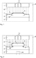
- the common process is to put the silicon wafers inside a recess on an aluminum substrate carrier plate as depicted in Fig. 1 .
- This substrate carrier plate does not only act as a holder for the silicon wafers (substrate), it also establishes the disc's thermal and electrical contacts to the actively cooled second (lower) electrode in the reaction chamber.
- the bevel on the silicon wafer facing the first (upper) electrode is exposed to the a-C:H depositing plasma while the remaining upper surface of the silicon wafer is covered by an aluminum shadow mask. Active cooling of the silicon wafer during the depositing process is necessary to avoid passivation layers with unsatisfactory electrical properties. Thermal degradation of a-C:H is reported in " Diamond-like amorphous carbon", by J. Robertson, Materials Science and Engineering: R: Reports 37, (2002) 129 .
- aligning or centering means can be used prior to loading the assembly into the reaction chamber of the plasma reactor.
Claims (4)
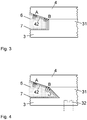
- Procédé pour appliquer un dépôt double face (7) de carbone hydrogéné amorphe sur une plaquette de silicium (4), ladite plaquette (4) comprenant un premier côté principal avec un premier biseau sur la bordure du premier côté principal et un deuxième côté principal qui présente une zone centrale et un deuxième biseau sur la bordure du deuxième côté principal entourant la zone centrale, ledit deuxième côté principal étant disposé à l'opposé du premier côté principal, comprenant les étapes consistant à monter la plaquette (4) sur un support de substrat surélevé (31) d'une plaque de support de substrat (3), ledit support de substrat (31) étant formé de telle sorte que la plaquette (4) soit placée sur le support de substrat (31) seulement avec sa zone centrale du deuxième côté principal en contact avec le support de substrat (31), et à placer la plaque de support de substrat avec la plaquette (4) dans une chambre de réaction (8) d'un réacteur à plasma, le premier et le deuxième biseau, du fait du support de substrat surélevé, étant exposés simultanément à un plasma (6) afin de créer le dépôt (7), du carbone hydrogène amorphe étant appliqué en tant que plasma.
- Procédé selon la revendication 1, dans lequel la température à l'intérieur de la plaquette est maintenue en dessous de 200°C au cours du processus de dépôt.
- Procédé selon l'une quelconque des revendications 1 ou 2, dans lequel la plaquette (4) est refroidie avant d'être montée sur la plaque de support de substrat (3) ou dans lequel la plaque de support de substrat (3) est refroidie avant d'être placée dans la chambre de réaction (8) ou dans lequel la plaquette (4) et la plaque de support de substrat (3) sont pré-refroidies avant que la plaquette ne soit exposée au plasma (6).
- Procédé selon l'une quelconque des revendications 1 à 3, dans lequel la chambre de réaction (8) comprend deux électrodes à plaques parallèles (1, 2), et dans lequel la plaquette (4) est refroidie activement au cours du processus de dépôt par des moyens de refroidissement (22) disposés dans les électrodes (2) de la chambre de réaction (8) ou dans lequel la plaquette (4) est refroidie activement au cours du processus de dépôt par des moyens de refroidissement (32) disposés dans la plaque de support de substrat (3) ou dans le support de substrat (31) de la plaque de support de substrat (3).
Priority Applications (7)
| Application Number | Priority Date | Filing Date | Title |
|---|---|---|---|
| EP08159693.4A EP2141259B1 (fr) | 2008-07-04 | 2008-07-04 | Procédé de dépôt pour la passivation de plaquettes de silicium |
| PCT/EP2009/058387 WO2010000830A1 (fr) | 2008-07-04 | 2009-07-03 | Procédé de dépôt pour passivation de tranches en silicium |
| RU2011103924/02A RU2509175C2 (ru) | 2008-07-04 | 2009-07-03 | Способ нанесения покрытия для пассивации кремниевых пластин |
| CN2009801256629A CN102084029B (zh) | 2008-07-04 | 2009-07-03 | 用于钝化硅晶片的沉积方法 |
| KR1020107029909A KR101571138B1 (ko) | 2008-07-04 | 2009-07-03 | 실리콘 웨이퍼의 패시베이션을 위한 증착 방법 |
| JP2011515467A JP2011526736A (ja) | 2008-07-04 | 2009-07-03 | シリコン・ウエーハのパッシベイションのための堆積方法 |
| US12/979,761 US8541317B2 (en) | 2008-07-04 | 2010-12-28 | Deposition method for passivation of silicon wafers |
Applications Claiming Priority (1)
| Application Number | Priority Date | Filing Date | Title |
|---|---|---|---|
| EP08159693.4A EP2141259B1 (fr) | 2008-07-04 | 2008-07-04 | Procédé de dépôt pour la passivation de plaquettes de silicium |
Publications (2)
| Publication Number | Publication Date |
|---|---|
| EP2141259A1 EP2141259A1 (fr) | 2010-01-06 |
| EP2141259B1 true EP2141259B1 (fr) | 2018-10-31 |
Family
ID=39831869
Family Applications (1)
| Application Number | Title | Priority Date | Filing Date |
|---|---|---|---|
| EP08159693.4A Active EP2141259B1 (fr) | 2008-07-04 | 2008-07-04 | Procédé de dépôt pour la passivation de plaquettes de silicium |
Country Status (7)
| Country | Link |
|---|---|
| US (1) | US8541317B2 (fr) |
| EP (1) | EP2141259B1 (fr) |
| JP (1) | JP2011526736A (fr) |
| KR (1) | KR101571138B1 (fr) |
| CN (1) | CN102084029B (fr) |
| RU (1) | RU2509175C2 (fr) |
| WO (1) | WO2010000830A1 (fr) |
Families Citing this family (4)
| Publication number | Priority date | Publication date | Assignee | Title |
|---|---|---|---|---|
| US10276797B2 (en) * | 2014-11-17 | 2019-04-30 | Sharp Kabushiki Kaisha | Vapor deposition device, vapor deposition method, and method for manufacturing organic electroluminescence element |
| RU2607110C1 (ru) * | 2015-07-09 | 2017-01-10 | Общество с ограниченной ответственностью "СВД.Спарк" | Держатель подложки |
| WO2017076659A1 (fr) | 2015-11-05 | 2017-05-11 | Abb Schweiz Ag | Dispositif semi-conducteur de puissance et procédé de production d'un dispositif semi-conducteur de puissance |
| RU2614080C1 (ru) * | 2015-12-16 | 2017-03-22 | Общество с ограниченной ответственностью "НТЦ тонкопленочных технологий в энергетике при ФТИ им. А.Ф. Иоффе", ООО "НТЦ ТПТ" | Пассивация поверхности кремниевых пластин методом магнетронного распыления |
Family Cites Families (16)
| Publication number | Priority date | Publication date | Assignee | Title |
|---|---|---|---|---|
| US623405A (en) * | 1899-04-18 | Vehicle-wheel | ||
| JPH043926A (ja) * | 1990-04-20 | 1992-01-08 | Sony Corp | 半導体装置の製造方法 |
| JPH06283500A (ja) * | 1993-03-30 | 1994-10-07 | Hitachi Ltd | 半導体製造装置および半導体装置 |
| JPH06333916A (ja) * | 1993-05-21 | 1994-12-02 | Fuji Electric Co Ltd | 非晶質カーボン膜の硬化方法 |
| US5384008A (en) * | 1993-06-18 | 1995-01-24 | Applied Materials, Inc. | Process and apparatus for full wafer deposition |
| US5822171A (en) | 1994-02-22 | 1998-10-13 | Applied Materials, Inc. | Electrostatic chuck with improved erosion resistance |
| US5883778A (en) * | 1994-02-28 | 1999-03-16 | Applied Materials, Inc. | Electrostatic chuck with fluid flow regulator |
| JPH08209352A (ja) * | 1995-02-06 | 1996-08-13 | Hitachi Ltd | プラズマ処理装置および方法 |
| US6641673B2 (en) * | 2000-12-20 | 2003-11-04 | General Electric Company | Fluid injector for and method of prolonged delivery and distribution of reagents into plasma |
| NL1017849C2 (nl) * | 2001-04-16 | 2002-10-30 | Univ Eindhoven Tech | Werkwijze en inrichting voor het deponeren van een althans ten dele kristallijne siliciumlaag op een substraat. |
| JP4714384B2 (ja) * | 2001-08-23 | 2011-06-29 | 株式会社アルバック | ウエハエッジ部分の処理方法及びプラズマ処理装置 |
| US20030072639A1 (en) | 2001-10-17 | 2003-04-17 | Applied Materials, Inc. | Substrate support |
| US20040112544A1 (en) * | 2002-12-16 | 2004-06-17 | Hongwen Yan | Magnetic mirror for preventing wafer edge damage during dry etching |
| US20050284371A1 (en) * | 2004-06-29 | 2005-12-29 | Mcfadden Robert S | Deposition apparatus for providing uniform low-k dielectric |
| US20070068623A1 (en) * | 2005-09-27 | 2007-03-29 | Yunsang Kim | Apparatus for the removal of a set of byproducts from a substrate edge and methods therefor |
| US7575982B2 (en) * | 2006-04-14 | 2009-08-18 | Applied Materials, Inc. | Stacked-substrate processes for production of nitride semiconductor structures |
-
2008
- 2008-07-04 EP EP08159693.4A patent/EP2141259B1/fr active Active
-
2009
- 2009-07-03 JP JP2011515467A patent/JP2011526736A/ja active Pending
- 2009-07-03 RU RU2011103924/02A patent/RU2509175C2/ru active
- 2009-07-03 CN CN2009801256629A patent/CN102084029B/zh active Active
- 2009-07-03 KR KR1020107029909A patent/KR101571138B1/ko active IP Right Grant
- 2009-07-03 WO PCT/EP2009/058387 patent/WO2010000830A1/fr active Application Filing
-
2010
- 2010-12-28 US US12/979,761 patent/US8541317B2/en active Active
Non-Patent Citations (1)
| Title |
|---|
| None * |
Also Published As
| Publication number | Publication date |
|---|---|
| CN102084029A (zh) | 2011-06-01 |
| CN102084029B (zh) | 2013-07-24 |
| JP2011526736A (ja) | 2011-10-13 |
| US20110189861A1 (en) | 2011-08-04 |
| RU2011103924A (ru) | 2012-08-10 |
| KR20110050598A (ko) | 2011-05-16 |
| KR101571138B1 (ko) | 2015-11-24 |
| US8541317B2 (en) | 2013-09-24 |
| EP2141259A1 (fr) | 2010-01-06 |
| WO2010000830A1 (fr) | 2010-01-07 |
| RU2509175C2 (ru) | 2014-03-10 |
Similar Documents
| Publication | Publication Date | Title |
|---|---|---|
| US10607867B2 (en) | Bolted wafer chuck thermal management systems and methods for wafer processing systems | |
| KR100733897B1 (ko) | 온도가 균일한 플라즈마 반응챔버 콤포넌트 | |
| US5228501A (en) | Physical vapor deposition clamping mechanism and heater/cooler | |
| US8441772B2 (en) | Substrate for electrostatic chuck and electrostatic chuck | |
| KR101903199B1 (ko) | 기판 상에 레이어를 증착하는 방법 및 장치 | |
| KR101110934B1 (ko) | 플라즈마 에칭용 고온 캐쏘오드 | |
| CN112053988A (zh) | 具有独立隔离的加热器区域的晶片载体 | |
| KR20010032700A (ko) | 프로세싱 챔버 및 플라즈마 구속방법 | |
| EP0452779B1 (fr) | Mécanisme de bridage pour déposition en phase gazeuse par procédé physique | |
| US10177014B2 (en) | Thermal radiation barrier for substrate processing chamber components | |
| TW202025217A (zh) | 具有嵌入式射頻屏蔽的半導體基板支撐件 | |
| TWI757242B (zh) | 用於晶圓處理系統的熱管理系統及方法 | |
| EP2141259B1 (fr) | Procédé de dépôt pour la passivation de plaquettes de silicium | |
| CN114686834A (zh) | 用于静电卡盘表面的径向向外的垫设计 | |
| WO2022082207A1 (fr) | Fuite de gaz côté arrière pour réduction de dépôt en biseau | |
| JP2001093863A (ja) | ウェーハ裏面スパッタリング方法及び半導体製造装置 | |
| KR102543933B1 (ko) | 냉각제 가스 존들 및 대응하는 그루브 및 단극성 정전 클램핑 전극 패턴들을 갖는 정전 척들 | |
| KR20120042383A (ko) | 기판 트레이 및 이를 이용하는 기판 처리장치 | |
| WO2020222764A1 (fr) | Ensembles sangle de mise à la terre | |
| CN201266602Y (zh) | 衬底承载板和沉积设备 | |
| US11605551B2 (en) | Chuck assembly, semiconductor device fabricating apparatus including the same, and method of fabricating semiconductor device | |
| JP2005294559A (ja) | ラジカル発生方法及びラジカル発生器、薄膜堆積装置 | |
| KR100787384B1 (ko) | 정전척 | |
| KR20080076432A (ko) | 플라즈마 처리 장치 | |
| US8367965B2 (en) | Electrode design for plasma processing chamber |
Legal Events
| Date | Code | Title | Description |
|---|---|---|---|
| PUAI | Public reference made under article 153(3) epc to a published international application that has entered the european phase |
Free format text: ORIGINAL CODE: 0009012 |
|
| AK | Designated contracting states |
Kind code of ref document: A1 Designated state(s): AT BE BG CH CY CZ DE DK EE ES FI FR GB GR HR HU IE IS IT LI LT LU LV MC MT NL NO PL PT RO SE SI SK TR |
|
| AX | Request for extension of the european patent |
Extension state: AL BA MK RS |
|
| 17P | Request for examination filed |
Effective date: 20100629 |
|
| 17Q | First examination report despatched |
Effective date: 20100723 |
|
| AKX | Designation fees paid |
Designated state(s): AT BE BG CH CY CZ DE DK EE ES FI FR GB GR HR HU IE IS IT LI LT LU LV MC MT NL NO PL PT RO SE SI SK TR |
|
| RAP1 | Party data changed (applicant data changed or rights of an application transferred) |
Owner name: ABB SCHWEIZ AG |
|
| GRAP | Despatch of communication of intention to grant a patent |
Free format text: ORIGINAL CODE: EPIDOSNIGR1 |
|
| STAA | Information on the status of an ep patent application or granted ep patent |
Free format text: STATUS: GRANT OF PATENT IS INTENDED |
|
| RIC1 | Information provided on ipc code assigned before grant |
Ipc: H01J 37/32 20060101ALI20180406BHEP Ipc: H01L 21/314 20060101ALI20180406BHEP Ipc: C23C 16/458 20060101AFI20180406BHEP Ipc: H01L 21/687 20060101ALI20180406BHEP |
|
| INTG | Intention to grant announced |
Effective date: 20180516 |
|
| GRAS | Grant fee paid |
Free format text: ORIGINAL CODE: EPIDOSNIGR3 |
|
| GRAA | (expected) grant |
Free format text: ORIGINAL CODE: 0009210 |
|
| STAA | Information on the status of an ep patent application or granted ep patent |
Free format text: STATUS: THE PATENT HAS BEEN GRANTED |
|
| AK | Designated contracting states |
Kind code of ref document: B1 Designated state(s): AT BE BG CH CY CZ DE DK EE ES FI FR GB GR HR HU IE IS IT LI LT LU LV MC MT NL NO PL PT RO SE SI SK TR |
|
| REG | Reference to a national code |
Ref country code: CH Ref legal event code: EP Ref country code: GB Ref legal event code: FG4D |
|
| RIN1 | Information on inventor provided before grant (corrected) |
Inventor name: AKURATI, KRANTHI Inventor name: JERVIS, RON Inventor name: KUNOW, MAGNUS Inventor name: ZIMMERMANN, ANDREAS |
|
| REG | Reference to a national code |
Ref country code: AT Ref legal event code: REF Ref document number: 1059484 Country of ref document: AT Kind code of ref document: T Effective date: 20181115 |
|
| REG | Reference to a national code |
Ref country code: IE Ref legal event code: FG4D |
|
| REG | Reference to a national code |
Ref country code: DE Ref legal event code: R096 Ref document number: 602008057646 Country of ref document: DE |
|
| REG | Reference to a national code |
Ref country code: NL Ref legal event code: MP Effective date: 20181031 |
|
| REG | Reference to a national code |
Ref country code: LT Ref legal event code: MG4D |
|
| REG | Reference to a national code |
Ref country code: AT Ref legal event code: MK05 Ref document number: 1059484 Country of ref document: AT Kind code of ref document: T Effective date: 20181031 |
|
| PG25 | Lapsed in a contracting state [announced via postgrant information from national office to epo] |
Ref country code: FI Free format text: LAPSE BECAUSE OF FAILURE TO SUBMIT A TRANSLATION OF THE DESCRIPTION OR TO PAY THE FEE WITHIN THE PRESCRIBED TIME-LIMIT Effective date: 20181031 Ref country code: NO Free format text: LAPSE BECAUSE OF FAILURE TO SUBMIT A TRANSLATION OF THE DESCRIPTION OR TO PAY THE FEE WITHIN THE PRESCRIBED TIME-LIMIT Effective date: 20190131 Ref country code: AT Free format text: LAPSE BECAUSE OF FAILURE TO SUBMIT A TRANSLATION OF THE DESCRIPTION OR TO PAY THE FEE WITHIN THE PRESCRIBED TIME-LIMIT Effective date: 20181031 Ref country code: ES Free format text: LAPSE BECAUSE OF FAILURE TO SUBMIT A TRANSLATION OF THE DESCRIPTION OR TO PAY THE FEE WITHIN THE PRESCRIBED TIME-LIMIT Effective date: 20181031 Ref country code: IS Free format text: LAPSE BECAUSE OF FAILURE TO SUBMIT A TRANSLATION OF THE DESCRIPTION OR TO PAY THE FEE WITHIN THE PRESCRIBED TIME-LIMIT Effective date: 20190228 Ref country code: LV Free format text: LAPSE BECAUSE OF FAILURE TO SUBMIT A TRANSLATION OF THE DESCRIPTION OR TO PAY THE FEE WITHIN THE PRESCRIBED TIME-LIMIT Effective date: 20181031 Ref country code: LT Free format text: LAPSE BECAUSE OF FAILURE TO SUBMIT A TRANSLATION OF THE DESCRIPTION OR TO PAY THE FEE WITHIN THE PRESCRIBED TIME-LIMIT Effective date: 20181031 Ref country code: PL Free format text: LAPSE BECAUSE OF FAILURE TO SUBMIT A TRANSLATION OF THE DESCRIPTION OR TO PAY THE FEE WITHIN THE PRESCRIBED TIME-LIMIT Effective date: 20181031 Ref country code: HR Free format text: LAPSE BECAUSE OF FAILURE TO SUBMIT A TRANSLATION OF THE DESCRIPTION OR TO PAY THE FEE WITHIN THE PRESCRIBED TIME-LIMIT Effective date: 20181031 Ref country code: BG Free format text: LAPSE BECAUSE OF FAILURE TO SUBMIT A TRANSLATION OF THE DESCRIPTION OR TO PAY THE FEE WITHIN THE PRESCRIBED TIME-LIMIT Effective date: 20190131 |
|
| PG25 | Lapsed in a contracting state [announced via postgrant information from national office to epo] |
Ref country code: GR Free format text: LAPSE BECAUSE OF FAILURE TO SUBMIT A TRANSLATION OF THE DESCRIPTION OR TO PAY THE FEE WITHIN THE PRESCRIBED TIME-LIMIT Effective date: 20190201 Ref country code: NL Free format text: LAPSE BECAUSE OF FAILURE TO SUBMIT A TRANSLATION OF THE DESCRIPTION OR TO PAY THE FEE WITHIN THE PRESCRIBED TIME-LIMIT Effective date: 20181031 Ref country code: SE Free format text: LAPSE BECAUSE OF FAILURE TO SUBMIT A TRANSLATION OF THE DESCRIPTION OR TO PAY THE FEE WITHIN THE PRESCRIBED TIME-LIMIT Effective date: 20181031 Ref country code: PT Free format text: LAPSE BECAUSE OF FAILURE TO SUBMIT A TRANSLATION OF THE DESCRIPTION OR TO PAY THE FEE WITHIN THE PRESCRIBED TIME-LIMIT Effective date: 20190301 |
|
| PG25 | Lapsed in a contracting state [announced via postgrant information from national office to epo] |
Ref country code: IT Free format text: LAPSE BECAUSE OF FAILURE TO SUBMIT A TRANSLATION OF THE DESCRIPTION OR TO PAY THE FEE WITHIN THE PRESCRIBED TIME-LIMIT Effective date: 20181031 Ref country code: CZ Free format text: LAPSE BECAUSE OF FAILURE TO SUBMIT A TRANSLATION OF THE DESCRIPTION OR TO PAY THE FEE WITHIN THE PRESCRIBED TIME-LIMIT Effective date: 20181031 Ref country code: DK Free format text: LAPSE BECAUSE OF FAILURE TO SUBMIT A TRANSLATION OF THE DESCRIPTION OR TO PAY THE FEE WITHIN THE PRESCRIBED TIME-LIMIT Effective date: 20181031 |
|
| REG | Reference to a national code |
Ref country code: DE Ref legal event code: R097 Ref document number: 602008057646 Country of ref document: DE |
|
| PG25 | Lapsed in a contracting state [announced via postgrant information from national office to epo] |
Ref country code: EE Free format text: LAPSE BECAUSE OF FAILURE TO SUBMIT A TRANSLATION OF THE DESCRIPTION OR TO PAY THE FEE WITHIN THE PRESCRIBED TIME-LIMIT Effective date: 20181031 Ref country code: SK Free format text: LAPSE BECAUSE OF FAILURE TO SUBMIT A TRANSLATION OF THE DESCRIPTION OR TO PAY THE FEE WITHIN THE PRESCRIBED TIME-LIMIT Effective date: 20181031 Ref country code: RO Free format text: LAPSE BECAUSE OF FAILURE TO SUBMIT A TRANSLATION OF THE DESCRIPTION OR TO PAY THE FEE WITHIN THE PRESCRIBED TIME-LIMIT Effective date: 20181031 |
|
| PLBE | No opposition filed within time limit |
Free format text: ORIGINAL CODE: 0009261 |
|
| STAA | Information on the status of an ep patent application or granted ep patent |
Free format text: STATUS: NO OPPOSITION FILED WITHIN TIME LIMIT |
|
| 26N | No opposition filed |
Effective date: 20190801 |
|
| PG25 | Lapsed in a contracting state [announced via postgrant information from national office to epo] |
Ref country code: SI Free format text: LAPSE BECAUSE OF FAILURE TO SUBMIT A TRANSLATION OF THE DESCRIPTION OR TO PAY THE FEE WITHIN THE PRESCRIBED TIME-LIMIT Effective date: 20181031 |
|
| PG25 | Lapsed in a contracting state [announced via postgrant information from national office to epo] |
Ref country code: MC Free format text: LAPSE BECAUSE OF FAILURE TO SUBMIT A TRANSLATION OF THE DESCRIPTION OR TO PAY THE FEE WITHIN THE PRESCRIBED TIME-LIMIT Effective date: 20181031 |
|
| REG | Reference to a national code |
Ref country code: CH Ref legal event code: PL |
|
| PG25 | Lapsed in a contracting state [announced via postgrant information from national office to epo] |
Ref country code: TR Free format text: LAPSE BECAUSE OF FAILURE TO SUBMIT A TRANSLATION OF THE DESCRIPTION OR TO PAY THE FEE WITHIN THE PRESCRIBED TIME-LIMIT Effective date: 20181031 |
|
| REG | Reference to a national code |
Ref country code: BE Ref legal event code: MM Effective date: 20190731 |
|
| PG25 | Lapsed in a contracting state [announced via postgrant information from national office to epo] |
Ref country code: BE Free format text: LAPSE BECAUSE OF NON-PAYMENT OF DUE FEES Effective date: 20190731 Ref country code: CH Free format text: LAPSE BECAUSE OF NON-PAYMENT OF DUE FEES Effective date: 20190731 Ref country code: LU Free format text: LAPSE BECAUSE OF NON-PAYMENT OF DUE FEES Effective date: 20190704 Ref country code: LI Free format text: LAPSE BECAUSE OF NON-PAYMENT OF DUE FEES Effective date: 20190731 |
|
| PG25 | Lapsed in a contracting state [announced via postgrant information from national office to epo] |
Ref country code: FR Free format text: LAPSE BECAUSE OF NON-PAYMENT OF DUE FEES Effective date: 20190731 |
|
| PG25 | Lapsed in a contracting state [announced via postgrant information from national office to epo] |
Ref country code: IE Free format text: LAPSE BECAUSE OF NON-PAYMENT OF DUE FEES Effective date: 20190704 |
|
| REG | Reference to a national code |
Ref country code: DE Ref legal event code: R081 Ref document number: 602008057646 Country of ref document: DE Owner name: HITACHI ENERGY SWITZERLAND AG, CH Free format text: FORMER OWNER: ABB SCHWEIZ AG, BADEN, CH Ref country code: DE Ref legal event code: R081 Ref document number: 602008057646 Country of ref document: DE Owner name: HITACHI ENERGY LTD, CH Free format text: FORMER OWNER: ABB SCHWEIZ AG, BADEN, CH Ref country code: DE Ref legal event code: R081 Ref document number: 602008057646 Country of ref document: DE Owner name: ABB POWER GRIDS SWITZERLAND AG, CH Free format text: FORMER OWNER: ABB SCHWEIZ AG, BADEN, CH |
|
| PG25 | Lapsed in a contracting state [announced via postgrant information from national office to epo] |
Ref country code: CY Free format text: LAPSE BECAUSE OF FAILURE TO SUBMIT A TRANSLATION OF THE DESCRIPTION OR TO PAY THE FEE WITHIN THE PRESCRIBED TIME-LIMIT Effective date: 20181031 |
|
| PG25 | Lapsed in a contracting state [announced via postgrant information from national office to epo] |
Ref country code: MT Free format text: LAPSE BECAUSE OF FAILURE TO SUBMIT A TRANSLATION OF THE DESCRIPTION OR TO PAY THE FEE WITHIN THE PRESCRIBED TIME-LIMIT Effective date: 20181031 Ref country code: HU Free format text: LAPSE BECAUSE OF FAILURE TO SUBMIT A TRANSLATION OF THE DESCRIPTION OR TO PAY THE FEE WITHIN THE PRESCRIBED TIME-LIMIT; INVALID AB INITIO Effective date: 20080704 |
|
| REG | Reference to a national code |
Ref country code: GB Ref legal event code: 732E Free format text: REGISTERED BETWEEN 20210923 AND 20210929 |
|
| REG | Reference to a national code |
Ref country code: DE Ref legal event code: R081 Ref document number: 602008057646 Country of ref document: DE Owner name: HITACHI ENERGY SWITZERLAND AG, CH Free format text: FORMER OWNER: ABB POWER GRIDS SWITZERLAND AG, BADEN, CH Ref country code: DE Ref legal event code: R081 Ref document number: 602008057646 Country of ref document: DE Owner name: HITACHI ENERGY LTD, CH Free format text: FORMER OWNER: ABB POWER GRIDS SWITZERLAND AG, BADEN, CH |
|
| P01 | Opt-out of the competence of the unified patent court (upc) registered |
Effective date: 20230527 |
|
| PGFP | Annual fee paid to national office [announced via postgrant information from national office to epo] |
Ref country code: GB Payment date: 20230720 Year of fee payment: 16 |
|
| PGFP | Annual fee paid to national office [announced via postgrant information from national office to epo] |
Ref country code: DE Payment date: 20230719 Year of fee payment: 16 |
|
| REG | Reference to a national code |
Ref country code: DE Ref legal event code: R082 Ref document number: 602008057646 Country of ref document: DE Representative=s name: DENNEMEYER & ASSOCIATES S.A., DE Ref country code: DE Ref legal event code: R081 Ref document number: 602008057646 Country of ref document: DE Owner name: HITACHI ENERGY LTD, CH Free format text: FORMER OWNER: HITACHI ENERGY SWITZERLAND AG, BADEN, CH |