EP2141259B1 - Deposition method for passivation of silicon wafers - Google Patents
Deposition method for passivation of silicon wafers Download PDFInfo
- Publication number
- EP2141259B1 EP2141259B1 EP08159693.4A EP08159693A EP2141259B1 EP 2141259 B1 EP2141259 B1 EP 2141259B1 EP 08159693 A EP08159693 A EP 08159693A EP 2141259 B1 EP2141259 B1 EP 2141259B1
- Authority
- EP
- European Patent Office
- Prior art keywords
- wafer
- carrier plate
- plasma
- substrate carrier
- substrate
- Prior art date
- Legal status (The legal status is an assumption and is not a legal conclusion. Google has not performed a legal analysis and makes no representation as to the accuracy of the status listed.)
- Active
Links
- XUIMIQQOPSSXEZ-UHFFFAOYSA-N Silicon Chemical compound [Si] XUIMIQQOPSSXEZ-UHFFFAOYSA-N 0.000 title claims description 62
- 229910052710 silicon Inorganic materials 0.000 title claims description 62
- 239000010703 silicon Substances 0.000 title claims description 62
- 235000012431 wafers Nutrition 0.000 title description 76
- 238000000151 deposition Methods 0.000 title description 19
- 238000002161 passivation Methods 0.000 title description 13
- 239000000758 substrate Substances 0.000 claims description 86
- 238000000034 method Methods 0.000 claims description 36
- 238000006243 chemical reaction Methods 0.000 claims description 16
- 230000008021 deposition Effects 0.000 claims description 15
- 238000001816 cooling Methods 0.000 claims description 14
- 238000005137 deposition process Methods 0.000 claims description 7
- 150000001721 carbon Chemical class 0.000 claims description 4
- 230000000903 blocking effect Effects 0.000 description 6
- 238000000623 plasma-assisted chemical vapour deposition Methods 0.000 description 6
- 239000007789 gas Substances 0.000 description 5
- VNWKTOKETHGBQD-UHFFFAOYSA-N methane Chemical compound C VNWKTOKETHGBQD-UHFFFAOYSA-N 0.000 description 4
- OKTJSMMVPCPJKN-UHFFFAOYSA-N Carbon Chemical compound [C] OKTJSMMVPCPJKN-UHFFFAOYSA-N 0.000 description 3
- 229910052782 aluminium Inorganic materials 0.000 description 3
- XAGFODPZIPBFFR-UHFFFAOYSA-N aluminium Chemical compound [Al] XAGFODPZIPBFFR-UHFFFAOYSA-N 0.000 description 3
- 229910052799 carbon Inorganic materials 0.000 description 3
- 230000005684 electric field Effects 0.000 description 3
- 150000002500 ions Chemical class 0.000 description 3
- 239000002243 precursor Substances 0.000 description 3
- 239000004065 semiconductor Substances 0.000 description 3
- 239000004215 Carbon black (E152) Substances 0.000 description 2
- HSFWRNGVRCDJHI-UHFFFAOYSA-N alpha-acetylene Natural products C#C HSFWRNGVRCDJHI-UHFFFAOYSA-N 0.000 description 2
- 230000003247 decreasing effect Effects 0.000 description 2
- 230000003628 erosive effect Effects 0.000 description 2
- 125000002534 ethynyl group Chemical group [H]C#C* 0.000 description 2
- 230000017525 heat dissipation Effects 0.000 description 2
- 229930195733 hydrocarbon Natural products 0.000 description 2
- 150000002430 hydrocarbons Chemical class 0.000 description 2
- 239000000463 material Substances 0.000 description 2
- XLYOFNOQVPJJNP-UHFFFAOYSA-N water Substances O XLYOFNOQVPJJNP-UHFFFAOYSA-N 0.000 description 2
- 235000001674 Agaricus brunnescens Nutrition 0.000 description 1
- 230000004913 activation Effects 0.000 description 1
- 229910003481 amorphous carbon Inorganic materials 0.000 description 1
- 230000015556 catabolic process Effects 0.000 description 1
- 239000004020 conductor Substances 0.000 description 1
- 238000006731 degradation reaction Methods 0.000 description 1
- 238000009792 diffusion process Methods 0.000 description 1
- 238000002513 implantation Methods 0.000 description 1
- 238000011065 in-situ storage Methods 0.000 description 1
- 239000011261 inert gas Substances 0.000 description 1
- 238000010884 ion-beam technique Methods 0.000 description 1
- 238000004518 low pressure chemical vapour deposition Methods 0.000 description 1
- 229910052751 metal Inorganic materials 0.000 description 1
- 239000002184 metal Substances 0.000 description 1
- 238000001465 metallisation Methods 0.000 description 1
- 238000004549 pulsed laser deposition Methods 0.000 description 1
- 238000004544 sputter deposition Methods 0.000 description 1
Images

Classifications
-
- C—CHEMISTRY; METALLURGY
- C23—COATING METALLIC MATERIAL; COATING MATERIAL WITH METALLIC MATERIAL; CHEMICAL SURFACE TREATMENT; DIFFUSION TREATMENT OF METALLIC MATERIAL; COATING BY VACUUM EVAPORATION, BY SPUTTERING, BY ION IMPLANTATION OR BY CHEMICAL VAPOUR DEPOSITION, IN GENERAL; INHIBITING CORROSION OF METALLIC MATERIAL OR INCRUSTATION IN GENERAL
- C23C—COATING METALLIC MATERIAL; COATING MATERIAL WITH METALLIC MATERIAL; SURFACE TREATMENT OF METALLIC MATERIAL BY DIFFUSION INTO THE SURFACE, BY CHEMICAL CONVERSION OR SUBSTITUTION; COATING BY VACUUM EVAPORATION, BY SPUTTERING, BY ION IMPLANTATION OR BY CHEMICAL VAPOUR DEPOSITION, IN GENERAL
- C23C16/00—Chemical coating by decomposition of gaseous compounds, without leaving reaction products of surface material in the coating, i.e. chemical vapour deposition [CVD] processes
- C23C16/44—Chemical coating by decomposition of gaseous compounds, without leaving reaction products of surface material in the coating, i.e. chemical vapour deposition [CVD] processes characterised by the method of coating
-
- H—ELECTRICITY
- H01—ELECTRIC ELEMENTS
- H01L—SEMICONDUCTOR DEVICES NOT COVERED BY CLASS H10
- H01L21/00—Processes or apparatus adapted for the manufacture or treatment of semiconductor or solid state devices or of parts thereof
- H01L21/67—Apparatus specially adapted for handling semiconductor or electric solid state devices during manufacture or treatment thereof; Apparatus specially adapted for handling wafers during manufacture or treatment of semiconductor or electric solid state devices or components ; Apparatus not specifically provided for elsewhere
- H01L21/683—Apparatus specially adapted for handling semiconductor or electric solid state devices during manufacture or treatment thereof; Apparatus specially adapted for handling wafers during manufacture or treatment of semiconductor or electric solid state devices or components ; Apparatus not specifically provided for elsewhere for supporting or gripping
- H01L21/687—Apparatus specially adapted for handling semiconductor or electric solid state devices during manufacture or treatment thereof; Apparatus specially adapted for handling wafers during manufacture or treatment of semiconductor or electric solid state devices or components ; Apparatus not specifically provided for elsewhere for supporting or gripping using mechanical means, e.g. chucks, clamps or pinches
- H01L21/68714—Apparatus specially adapted for handling semiconductor or electric solid state devices during manufacture or treatment thereof; Apparatus specially adapted for handling wafers during manufacture or treatment of semiconductor or electric solid state devices or components ; Apparatus not specifically provided for elsewhere for supporting or gripping using mechanical means, e.g. chucks, clamps or pinches the wafers being placed on a susceptor, stage or support
- H01L21/68735—Apparatus specially adapted for handling semiconductor or electric solid state devices during manufacture or treatment thereof; Apparatus specially adapted for handling wafers during manufacture or treatment of semiconductor or electric solid state devices or components ; Apparatus not specifically provided for elsewhere for supporting or gripping using mechanical means, e.g. chucks, clamps or pinches the wafers being placed on a susceptor, stage or support characterised by edge profile or support profile
-
- C—CHEMISTRY; METALLURGY
- C23—COATING METALLIC MATERIAL; COATING MATERIAL WITH METALLIC MATERIAL; CHEMICAL SURFACE TREATMENT; DIFFUSION TREATMENT OF METALLIC MATERIAL; COATING BY VACUUM EVAPORATION, BY SPUTTERING, BY ION IMPLANTATION OR BY CHEMICAL VAPOUR DEPOSITION, IN GENERAL; INHIBITING CORROSION OF METALLIC MATERIAL OR INCRUSTATION IN GENERAL
- C23C—COATING METALLIC MATERIAL; COATING MATERIAL WITH METALLIC MATERIAL; SURFACE TREATMENT OF METALLIC MATERIAL BY DIFFUSION INTO THE SURFACE, BY CHEMICAL CONVERSION OR SUBSTITUTION; COATING BY VACUUM EVAPORATION, BY SPUTTERING, BY ION IMPLANTATION OR BY CHEMICAL VAPOUR DEPOSITION, IN GENERAL
- C23C16/00—Chemical coating by decomposition of gaseous compounds, without leaving reaction products of surface material in the coating, i.e. chemical vapour deposition [CVD] processes
- C23C16/04—Coating on selected surface areas, e.g. using masks
- C23C16/042—Coating on selected surface areas, e.g. using masks using masks
-
- C—CHEMISTRY; METALLURGY
- C23—COATING METALLIC MATERIAL; COATING MATERIAL WITH METALLIC MATERIAL; CHEMICAL SURFACE TREATMENT; DIFFUSION TREATMENT OF METALLIC MATERIAL; COATING BY VACUUM EVAPORATION, BY SPUTTERING, BY ION IMPLANTATION OR BY CHEMICAL VAPOUR DEPOSITION, IN GENERAL; INHIBITING CORROSION OF METALLIC MATERIAL OR INCRUSTATION IN GENERAL
- C23C—COATING METALLIC MATERIAL; COATING MATERIAL WITH METALLIC MATERIAL; SURFACE TREATMENT OF METALLIC MATERIAL BY DIFFUSION INTO THE SURFACE, BY CHEMICAL CONVERSION OR SUBSTITUTION; COATING BY VACUUM EVAPORATION, BY SPUTTERING, BY ION IMPLANTATION OR BY CHEMICAL VAPOUR DEPOSITION, IN GENERAL
- C23C16/00—Chemical coating by decomposition of gaseous compounds, without leaving reaction products of surface material in the coating, i.e. chemical vapour deposition [CVD] processes
- C23C16/22—Chemical coating by decomposition of gaseous compounds, without leaving reaction products of surface material in the coating, i.e. chemical vapour deposition [CVD] processes characterised by the deposition of inorganic material, other than metallic material
- C23C16/26—Deposition of carbon only
-
- C—CHEMISTRY; METALLURGY
- C23—COATING METALLIC MATERIAL; COATING MATERIAL WITH METALLIC MATERIAL; CHEMICAL SURFACE TREATMENT; DIFFUSION TREATMENT OF METALLIC MATERIAL; COATING BY VACUUM EVAPORATION, BY SPUTTERING, BY ION IMPLANTATION OR BY CHEMICAL VAPOUR DEPOSITION, IN GENERAL; INHIBITING CORROSION OF METALLIC MATERIAL OR INCRUSTATION IN GENERAL
- C23C—COATING METALLIC MATERIAL; COATING MATERIAL WITH METALLIC MATERIAL; SURFACE TREATMENT OF METALLIC MATERIAL BY DIFFUSION INTO THE SURFACE, BY CHEMICAL CONVERSION OR SUBSTITUTION; COATING BY VACUUM EVAPORATION, BY SPUTTERING, BY ION IMPLANTATION OR BY CHEMICAL VAPOUR DEPOSITION, IN GENERAL
- C23C16/00—Chemical coating by decomposition of gaseous compounds, without leaving reaction products of surface material in the coating, i.e. chemical vapour deposition [CVD] processes
- C23C16/44—Chemical coating by decomposition of gaseous compounds, without leaving reaction products of surface material in the coating, i.e. chemical vapour deposition [CVD] processes characterised by the method of coating
- C23C16/458—Chemical coating by decomposition of gaseous compounds, without leaving reaction products of surface material in the coating, i.e. chemical vapour deposition [CVD] processes characterised by the method of coating characterised by the method used for supporting substrates in the reaction chamber
- C23C16/4582—Rigid and flat substrates, e.g. plates or discs
- C23C16/4583—Rigid and flat substrates, e.g. plates or discs the substrate being supported substantially horizontally
-
- C—CHEMISTRY; METALLURGY
- C23—COATING METALLIC MATERIAL; COATING MATERIAL WITH METALLIC MATERIAL; CHEMICAL SURFACE TREATMENT; DIFFUSION TREATMENT OF METALLIC MATERIAL; COATING BY VACUUM EVAPORATION, BY SPUTTERING, BY ION IMPLANTATION OR BY CHEMICAL VAPOUR DEPOSITION, IN GENERAL; INHIBITING CORROSION OF METALLIC MATERIAL OR INCRUSTATION IN GENERAL
- C23C—COATING METALLIC MATERIAL; COATING MATERIAL WITH METALLIC MATERIAL; SURFACE TREATMENT OF METALLIC MATERIAL BY DIFFUSION INTO THE SURFACE, BY CHEMICAL CONVERSION OR SUBSTITUTION; COATING BY VACUUM EVAPORATION, BY SPUTTERING, BY ION IMPLANTATION OR BY CHEMICAL VAPOUR DEPOSITION, IN GENERAL
- C23C16/00—Chemical coating by decomposition of gaseous compounds, without leaving reaction products of surface material in the coating, i.e. chemical vapour deposition [CVD] processes
- C23C16/44—Chemical coating by decomposition of gaseous compounds, without leaving reaction products of surface material in the coating, i.e. chemical vapour deposition [CVD] processes characterised by the method of coating
- C23C16/50—Chemical coating by decomposition of gaseous compounds, without leaving reaction products of surface material in the coating, i.e. chemical vapour deposition [CVD] processes characterised by the method of coating using electric discharges
- C23C16/503—Chemical coating by decomposition of gaseous compounds, without leaving reaction products of surface material in the coating, i.e. chemical vapour deposition [CVD] processes characterised by the method of coating using electric discharges using dc or ac discharges
-
- H—ELECTRICITY
- H01—ELECTRIC ELEMENTS
- H01J—ELECTRIC DISCHARGE TUBES OR DISCHARGE LAMPS
- H01J37/00—Discharge tubes with provision for introducing objects or material to be exposed to the discharge, e.g. for the purpose of examination or processing thereof
- H01J37/32—Gas-filled discharge tubes
- H01J37/32431—Constructional details of the reactor
- H01J37/32733—Means for moving the material to be treated
-
- H—ELECTRICITY
- H01—ELECTRIC ELEMENTS
- H01L—SEMICONDUCTOR DEVICES NOT COVERED BY CLASS H10
- H01L21/00—Processes or apparatus adapted for the manufacture or treatment of semiconductor or solid state devices or of parts thereof
- H01L21/02—Manufacture or treatment of semiconductor devices or of parts thereof
- H01L21/02104—Forming layers
- H01L21/02107—Forming insulating materials on a substrate
- H01L21/02109—Forming insulating materials on a substrate characterised by the type of layer, e.g. type of material, porous/non-porous, pre-cursors, mixtures or laminates
- H01L21/02112—Forming insulating materials on a substrate characterised by the type of layer, e.g. type of material, porous/non-porous, pre-cursors, mixtures or laminates characterised by the material of the layer
- H01L21/02115—Forming insulating materials on a substrate characterised by the type of layer, e.g. type of material, porous/non-porous, pre-cursors, mixtures or laminates characterised by the material of the layer the material being carbon, e.g. alpha-C, diamond or hydrogen doped carbon
-
- H—ELECTRICITY
- H01—ELECTRIC ELEMENTS
- H01L—SEMICONDUCTOR DEVICES NOT COVERED BY CLASS H10
- H01L21/00—Processes or apparatus adapted for the manufacture or treatment of semiconductor or solid state devices or of parts thereof
- H01L21/02—Manufacture or treatment of semiconductor devices or of parts thereof
- H01L21/02104—Forming layers
- H01L21/02107—Forming insulating materials on a substrate
- H01L21/02225—Forming insulating materials on a substrate characterised by the process for the formation of the insulating layer
- H01L21/0226—Forming insulating materials on a substrate characterised by the process for the formation of the insulating layer formation by a deposition process
- H01L21/02263—Forming insulating materials on a substrate characterised by the process for the formation of the insulating layer formation by a deposition process deposition from the gas or vapour phase
- H01L21/02271—Forming insulating materials on a substrate characterised by the process for the formation of the insulating layer formation by a deposition process deposition from the gas or vapour phase deposition by decomposition or reaction of gaseous or vapour phase compounds, i.e. chemical vapour deposition
- H01L21/02274—Forming insulating materials on a substrate characterised by the process for the formation of the insulating layer formation by a deposition process deposition from the gas or vapour phase deposition by decomposition or reaction of gaseous or vapour phase compounds, i.e. chemical vapour deposition in the presence of a plasma [PECVD]
-
- H—ELECTRICITY
- H01—ELECTRIC ELEMENTS
- H01L—SEMICONDUCTOR DEVICES NOT COVERED BY CLASS H10
- H01L21/00—Processes or apparatus adapted for the manufacture or treatment of semiconductor or solid state devices or of parts thereof
- H01L21/02—Manufacture or treatment of semiconductor devices or of parts thereof
- H01L21/02104—Forming layers
- H01L21/02365—Forming inorganic semiconducting materials on a substrate
- H01L21/02612—Formation types
- H01L21/02617—Deposition types
- H01L21/0262—Reduction or decomposition of gaseous compounds, e.g. CVD
-
- H—ELECTRICITY
- H01—ELECTRIC ELEMENTS
- H01L—SEMICONDUCTOR DEVICES NOT COVERED BY CLASS H10
- H01L21/00—Processes or apparatus adapted for the manufacture or treatment of semiconductor or solid state devices or of parts thereof
- H01L21/02—Manufacture or treatment of semiconductor devices or of parts thereof
- H01L21/04—Manufacture or treatment of semiconductor devices or of parts thereof the devices having at least one potential-jump barrier or surface barrier, e.g. PN junction, depletion layer or carrier concentration layer
- H01L21/18—Manufacture or treatment of semiconductor devices or of parts thereof the devices having at least one potential-jump barrier or surface barrier, e.g. PN junction, depletion layer or carrier concentration layer the devices having semiconductor bodies comprising elements of Group IV of the Periodic System or AIIIBV compounds with or without impurities, e.g. doping materials
- H01L21/30—Treatment of semiconductor bodies using processes or apparatus not provided for in groups H01L21/20 - H01L21/26
- H01L21/31—Treatment of semiconductor bodies using processes or apparatus not provided for in groups H01L21/20 - H01L21/26 to form insulating layers thereon, e.g. for masking or by using photolithographic techniques; After treatment of these layers; Selection of materials for these layers
- H01L21/314—Inorganic layers
- H01L21/3146—Carbon layers, e.g. diamond-like layers
-
- H—ELECTRICITY
- H01—ELECTRIC ELEMENTS
- H01L—SEMICONDUCTOR DEVICES NOT COVERED BY CLASS H10
- H01L21/00—Processes or apparatus adapted for the manufacture or treatment of semiconductor or solid state devices or of parts thereof
- H01L21/67—Apparatus specially adapted for handling semiconductor or electric solid state devices during manufacture or treatment thereof; Apparatus specially adapted for handling wafers during manufacture or treatment of semiconductor or electric solid state devices or components ; Apparatus not specifically provided for elsewhere
- H01L21/683—Apparatus specially adapted for handling semiconductor or electric solid state devices during manufacture or treatment thereof; Apparatus specially adapted for handling wafers during manufacture or treatment of semiconductor or electric solid state devices or components ; Apparatus not specifically provided for elsewhere for supporting or gripping
- H01L21/687—Apparatus specially adapted for handling semiconductor or electric solid state devices during manufacture or treatment thereof; Apparatus specially adapted for handling wafers during manufacture or treatment of semiconductor or electric solid state devices or components ; Apparatus not specifically provided for elsewhere for supporting or gripping using mechanical means, e.g. chucks, clamps or pinches
- H01L21/68714—Apparatus specially adapted for handling semiconductor or electric solid state devices during manufacture or treatment thereof; Apparatus specially adapted for handling wafers during manufacture or treatment of semiconductor or electric solid state devices or components ; Apparatus not specifically provided for elsewhere for supporting or gripping using mechanical means, e.g. chucks, clamps or pinches the wafers being placed on a susceptor, stage or support
- H01L21/68785—Apparatus specially adapted for handling semiconductor or electric solid state devices during manufacture or treatment thereof; Apparatus specially adapted for handling wafers during manufacture or treatment of semiconductor or electric solid state devices or components ; Apparatus not specifically provided for elsewhere for supporting or gripping using mechanical means, e.g. chucks, clamps or pinches the wafers being placed on a susceptor, stage or support characterised by the mechanical construction of the susceptor, stage or support
Description
- Subject matter disclosed herein relates generally to the technical field of high-voltage, high-power semiconductors and, in particular, to a method and an apparatus for a single-step double-sided deposition of an electrical passivation layer on silicon wafers for power semiconductors.
- In general, bipolar power semiconductors, such as diodes, thyristors, GTOs and GCTs, are made from silicon wafers. After these silicon wafers have undergone different implantation, diffusion, photolithographic and metallization processes, they are cut to circular discs and a negative or positive bevel is ground on the high-voltage blocking pn-junction(s). These bevels usually need to be protected with an electric passivation layer. One of the currently used state of the art passivation materials is amorphous hydrogenated carbon (a-C:H, also known as Diamond-like carbon DLC) which is typically deposited in a Plasma Enhanced Chemical Vapor Deposition (PECVD) process inside a parallel plate plasma reactor, but could generally be deposited in PECVD reactors of other geometries or by ion beam, sputtering, cathodic arc, pulsed laser deposition or low pressure CVD.
- A simplified picture of the general PECVD process is given in
Fig. 1 . The silicon wafer is in contact with the second, lower electrode inside the reaction chamber via a substrate carrier plate. The hydrocarbon precursor gas (e.g., methane, acetylene) enters the reaction chamber of the plasma reactor through openings in the first, upper electrode, is ionized by radiofrequency, and forms the bulk plasma. The edge plasma layer is the space where the plasma ions get accelerated into the direction of the substrate and substrate carrier plate due to a DC bias voltage applied between the two electrodes. - The common process is to put the silicon wafers inside a recess on an aluminum substrate carrier plate as depicted in
Fig. 1 . This substrate carrier plate does not only act as a holder for the silicon wafers (substrate), it also establishes the disc's thermal and electrical contacts to the actively cooled second (lower) electrode in the reaction chamber. The bevel on the silicon wafer facing the first (upper) electrode is exposed to the a-C:H depositing plasma while the remaining upper surface of the silicon wafer is covered by an aluminum shadow mask. Active cooling of the silicon wafer during the depositing process is necessary to avoid passivation layers with unsatisfactory electrical properties. Thermal degradation of a-C:H is reported in "Diamond-like amorphous carbon", by J. Robertson, Materials Science and Engineering: R: Reports 37, (2002) 129. - Silicon wafers with two high voltage blocking pn-junctions (e.g., a thyristor) may have one negative bevel ground on each of its opposite sides. With the common process described above, only the upper bevel is coated with a-C:H in a single process run. As a result, manual flipping-over of the silicon wafer and a second a-C:H deposit-process run are required. Since the bevel coated in the second process step is put into the recess face-down during the first process step in an unprotected and very sensitive state, said bevel is at a high risk of being contaminated resulting in a reduced blocking yield.
- From
US 6,023,405 a support plate is known for holding a wafer in a process chamber of a plasma reactor. The wafer is slightly larger than the support in order to let gas flow through a channel at the border of the support. If erosive process gases are present in the chamber, inert gases can flow through the channel to avoid erosion on the support. Therefore, this small cross section of the support compared to the wafer size is neither intended nor suitable for applying the plasma to bevels of a wafer. Shape and size of the support shall be the same as the shape and size of the wafer in order to maximize heat transfer and to maximize the contact area. - It is an object of the invention to reveal a single-step method for the deposition of an double-sided deposition as an electrical passivation layer, such as a homogeneous a-C:H layer, on two sides of a silicon wafer.
- The inventive method is based on Plasma Enhanced Chemical Vapor Deposition (PECVP) in combination with an improved substrate-holder apparatus. The inventive method comprises the step of mounting a silicon wafer on an elevated substrate support of a substrate carrier plate and placing the substrate carrier plate with the silicon wafer in a plasma reactor. The substrate support is formed such that the wafer is placed on the substrate support only with its central area of the second main side being in contact to the substrate support. Due to such an elevated substrate support, both opposite sides of the silicon wafer are exposed to the plasma and are therefore coated with an electrical passivation layer. By the electrical passivation layer the wafer is electrically inactivated in the area of the electrical passivation layer (The inventive passivation layer is not completely electrically inactive while it is partially conductive.).
- The inventive method is advantageous over former methods as a-C:H-layers are deposited on two sides of the wafer, e.g. a silicon wafer, in one process step, either both on the two sides of one silicon wafer or on two silicon wafers stacked back to back. The wafer comprises a first main side with a first bevel on the border of the first main side and a second main side, which has a central area and a second bevel on the border of the second main side surrounding the central area, which second main side is arranged opposite the first main side. The wafer is mounted on a substrate support of a substrate carrier plate, which substrate support is formed such that the wafer is placed on the substrate support only with its central area of the second main side being in contact to the substrate support. Then the substrate carrier plate is placed with the wafer in a reaction chamber of a plasma reactor. Thereby, the first and second bevels are exposed simultaneously to the plasma in order to create the electrical passivation layer. In an exemplary embodiment, amorphous hydrogenated carbon is applied as the plasma to form the electrical passivation layer onto the wafer.
- In order to avoid deteriorated heat transfer which may occur due to the increased distance between the silicon wafer carried on the elevated substrate support of the substrate carrier plate and the actively cooled lower electrode, the invention also relates to a combination of said novel substrate carrier plate design and an improved silicon wafer cooling mechanism. This allows for reasonable heat dissipation, which is crucial for the deposition process, since more graphite-like carbon layers with unsatisfactory electrical properties may be deposited at substrate temperatures above approximately 200 °C.
- The described invention highlights the significance of a pedestal-like substrate carrier plate instead of a recess. Therefore, both sides of a silicon wafer are exposed to the plasma. Nevertheless, homogeneous deposition is highly non-trivial, especially for the bevel adjacent to the lower electrode. As both even plasma flux-rates and homogeneous electric fields are necessary for the deposition of uniform a-C:H-layers, mushroom-shaped (e.g. concave, upside down truncated cone, etc.) designs of the elevated substrate supports tend to be advantageous over purely cylindrical designs.
- In yet another embodiment, the invention also relates to adjusted deposit-process parameters of the DC bias voltage.
- A more complete understanding of the invention may be gained by reference to the following detailed description when taken in conjunction with the accompanying drawings wherein:
-
Fig. 1 schematically shows an assembly with a silicon wafer within a parallel plate reactor in a prior art single sided deposition process, -
Fig. 2 schematically shows an assembly with a silicon wafer on an inventive elevated substrate support within a parallel plate reactor, -
Fig. 3 shows in more detail the assembly ofFig. 2 , with a first embodiment (cylindrical) of the inventive elevated substrate support, -
Fig. 4 shows in more detail the assembly ofFig. 2 , with a second embodiment (truncated cone) of the inventive elevated substrate support, and -
Fig. 5 schematically shows an assembly with stacked silicon wafers on inventive elevated substrate supports within a parallel plate reactor. -
Fig. 1 provides a schematic drawing of a parallel plate reactor used in a prior art PECVD-process with a pair ofparallel plate electrodes reaction chamber 8,bulk plasma 6,edge plasma layer 7,silicon wafer 4,shadow mask 5, andsubstrate carrier plate 3 withrecess 33. Electron energy (plasma) is used as the activation method to enable a-C:H deposition on the silicon wafer. The hydrocarbon precursor gas (e.g., methane, acetylene) enters thereaction chamber 8 throughopenings 11 in theupper electrode 1. It is ionized by radiofrequency and forms thebulk plasma 6. Theedge plasma layer 7 is the space in thereaction chamber 8 where plasma ions get accelerated to the silicon wafer or substrate carrier plate due to a DC bias voltage that has been applied between the twoelectrodes silicon wafer 4 as a substrate is put inside arecess 33 on asubstrate carrier plate 3. Thissubstrate carrier plate 3 does not only act as a mechanical substrate holder, but it also establishes thermal and electrical contacts between the silicon wafer and thelower electrode 2 in thereaction chamber 8 of the plasma reactor. One bevel on the silicon wafer that is to be passivated is facing theupper electrode 1. This bevel is exposed to the a-C:H depositing plasma 6 and/or 7. Areas on the top surface of the silicon wafer that are not subject to passivation are covered by ashadow mask 5. In the current process, only the upper bevel is coated with a-C:H in a single process run. As a result, manual flipping-over of the silicon wafer and a second a-C:H deposit-process run are required for silicon wafer with two high voltage blocking pn-junctions, that have one bevel on each opposite side (e.g., a thyristor). As mentioned above, the bevel coated in the second process step is put into therecess 33 face-down (in an unprotected and therefore very sensitive state) during the first process step and is therefore at a high risk of being contaminated resulting in a reduced blocking yield. -
Fig. 2 provides a schematic drawing of an improved version of a parallel plate reactor used in the inventive one-step double-sided PECVD-process. The apparatus differs from the one used inFig. 1 in so far that a newly developedsubstrate carrier plate 3 is used. This plate is preferably made of electrically and thermally conducting material, such as aluminum or another metal. The silicon wafer substrate is no longer placed inside a recess in thesubstrate carrier plate 3, in order to overcome the limitation of only single-sided a-C:H-deposition. Instead, the silicon wafer is placed on top of a "mushroom-like" or "pedestal-like" protrusion, which is referred to aselevated substrate support 31. The wafer is placed on thesubstrate carrier plate 3 with a contact area of such a design, that the second main side of the wafer is in contact to thesubstrate carrier plate 31 and the first and second bevels are not covered or enclosed or encased by thesubstrate carrier plate 31. - Said
elevated substrate support 31 is arranged on top of thesubstrate carrier plate 3, integrated in thesubstrate carrier plate 3 or optionally as a separate part. This substrate carrier plate does not only act as a mechanical substrate holder for the silicon wafer, but it also establishes thermal and electrical contacts between the silicon wafer and thelower electrode 2 in thereaction chamber 8. By lifting the position of the silicon wafer, flow of plasma, which again is created from precursor gases flowing into thereaction chamber 8 through theparallel plate electrode 1, is no longer limited to theupper bevels 41 of the silicon wafer substrate. The a-C:H-deposition simultaneously occurs on theupper bevels 41 and lover bevels 42 of the silicon wafer. The non-coatable upper surface areas of the silicon wafer are again covered by ashadow mask 5. To indirectly limit the temperature of the silicon wafer to a level below approximately 200 °C, thebottom electrode 2 is actively cooled, e.g. by awater cooling device 22 running at a temperature of about 15 to 20 °C. -
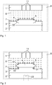
Fig. 3 provides a more detailed view of a first embodiment of an inventive "pedestal-like"elevated substrate support 31 of thesubstrate carrier plate 3 with the silicon wafer on top. Ions from thebulk plasma 6 get accelerated to thesilicon wafer 4 in theedge plasma layer 7 near the surfaces that are electrically connected to thebottom electrode 2. Homogeneous a-C:H deposition on thesilicon wafer 4 at different regions A and B is highly non-trivial especially for the lower bevel on the silicon wafer. The reason is that evenly distributed plasma flux-rates and homogeneous electric fields are necessary for the deposition of uniform a-C:H-layers. However, except for extremely small plasma edge layer thicknesses, the plasma-flux density as well as the accelerating electric field can differ for regions A and B resulting in slightly inhomogeneous a-C:H deposition in these regions. To a certain extent, such inhomogenities can be compensated for by a slight tuning of the process parameters, as the plasma edge layer thickness scales with the square root of the DC bias voltage which can be decreased to a minimum of approximately 500 Volts. This minimal DC bias voltage may vary for some reactors, as it is dependant of many different parameters. -
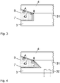
Fig. 4 provides a more detailed view of a second embodiment of the inventivesubstrate carrier plate 3, in particular theelevated substrate support 31. Instead of using a mere cylindrical protrusion aselevated substrate support 31 of thesubstrate carrier plate 3, an additional rotated cut at the base leads to a concave cross-section of theelevated substrate support 31. Regarding this type of geometrical profile, these elevated substrate supports are herein referred to as "mushroom-shaped". Possible geometrical cut, mushroom shaped, profiles are not limited to straight lines. In principle, any geometrical profile of theelevated substrate support 31 can be used, e.g. concave, upside down truncated cone, etc., provided that plasma flux-rates are sufficiently high and electric/ magnetic fields on the bottom bevels of the silicon wafer are such as to provide a deposition rate as homogeneous as possible. In these cases, homogeneous a-C:H deposition on thesilicon wafer 4 at different regions A and B is facilitated. Remaining possible inhomogenities can again be compensated for by a slight tuning of the process parameters, as the plasma edge layer thickness scales with the square root of the DC bias voltage which can be decreased to a minimum of approximately 500 V. Improved and more direct cooling of the silicon wafer is optionally achieved by active cooling with acooling device 32 arranged in or adjacent to thesubstrate carrier plate 3 or in or adjacent to theelevated substrate support 31 of the substrate carrier plate. As cooling device, water cooling can be used, operating for example at a temperature of 15 to 20 °C. This optimized in-situ cooling strategy in combination with an optional pre-cooling procedure of the silicon wafer and/ or the substrate carrier plate leads to a maximal process temperature of the silicon wafer of below 200 °C. In order to further reduce the temperature of the silicon wafer during the deposition process cooling means are optionally arranged in the shadow mask, which is covering an upper surface of the silicon wafer. As mentioned above, satisfactory heat dissipation is crucial for the deposition process as silicon wafer temperatures above 200 °C may lead to the deposition of graphite-like carbon layers with unsatisfactory electrical properties. - In order to properly align, i.e. concentrically align,
silicon wafer 4 andelevated substrate support 31 of thesubstrate carrier plate 3, aligning or centering means can be used prior to loading the assembly into the reaction chamber of the plasma reactor. - Optionally, as schematically shown in
Fig. 5 , additional silicon wafers 4' may be stacked on top of the onesilicon wafer 4 carried on theelevated substrate support 31. Betweenadjacent silicon wafers 4 and 4' in the stack, an elevated substrate support 31' is arranged, in order to allow homogeneous a-C:H deposition on adjacent silicon wafers. Optionally, this additional elevated substrate support may be omitted, to allow back-to-back stacking of two silicon wafers, each with only one high voltage blocking pn-junction, such as diodes, GTOs and GCTs, and therefore only one bevel to be passivated. - Optionally, cooling means may be arranged within the additional elevated substrate supports 31' and/ or the
shadow mask 5, arranged on top of the stack. Optionally, there is anelectrically conducting connection 34 arranged between the additional elevated substrate supports 31' and one or several or all of the parts, which are electrically connected to thelower electrode 2, i.e. theelevated substrate support 31, thesubstrate carrier plate 3 or thelower electrode 2 itself. -
- 1, 2
- Electrodes
- 22
- cooler
- 3
- substrate carrier plate
- 31, 31'
- Elevated Substrate support
- 32
- cooler
- 33
- recess
- 34
- electrically conducting connection
- 4, 4'
- Si-disc/ substrate
- 41
- Upper bevel
- 42
- Lower bevel
- 5
- Shadow mask
- 6
- bulk plasma
- 7
- edge plasma layer
- 8
- Reaction chamber of plasma reactor
Claims (4)
- Method for applying double-sided deposition (7) of amorphous hydrogenated carbon onto a silicon wafer (4), which wafer (4) comprises a first main side with a first bevel on the border of the first main side and a second main side, which has a central area and a second bevel on the border of the second main side surrounding the central area, which second main side is arranged opposite the first main side, comprising the steps of mounting the wafer (4) on an elevated substrate support (31) of a substrate carrier plate (3), which substrate support (31) is formed such that the wafer (4) is placed on the substrate support (31) only with its central area of the second main side being in contact to the substrate support (31), and placing the substrate carrier plate with the wafer (4) in a reaction chamber (8) of a plasma reactor, wherein, due to the elevated substrate support, the first and second bevels are exposed simultaneously to a plasma (6) in order to create the deposition (7), wherein amorphous hydrogenated carbon is applied as the plasma.
- Method as in claim 1, wherein the temperature within the wafer is kept below 200 °C during the deposition process.
- Method as in one of the claims 1 or 2, wherein the wafer (4) is cooled prior to being mounted on the substrate carrier plate (3) or wherein the substrate carrier plate (3) is cooled prior to being placed in the reaction chamber (8) or wherein the wafer (4) and the substrate carrier plate (3) are pre-cooled before the wafer is exposed to the plasma (6).
- Method as in one of the claims 1 to 3, wherein the reaction chamber (8) comprises two parallel plate electrodes (1, 2) and wherein the wafer (4) is being actively cooled during the deposition process by cooling means (22) arranged in the electrodes (2) of the reaction chamber (8) or wherein the wafer (4) is being actively cooled during the deposition process by cooling means (32) arranged in the substrate carrier plate (3) or the substrate support (31) of the substrate carrier plate (3).
Priority Applications (7)
| Application Number | Priority Date | Filing Date | Title |
|---|---|---|---|
| EP08159693.4A EP2141259B1 (en) | 2008-07-04 | 2008-07-04 | Deposition method for passivation of silicon wafers |
| CN2009801256629A CN102084029B (en) | 2008-07-04 | 2009-07-03 | Deposition method for passivation of silicon wafers |
| KR1020107029909A KR101571138B1 (en) | 2008-07-04 | 2009-07-03 | Deposition method for passivation of silicon wafers |
| PCT/EP2009/058387 WO2010000830A1 (en) | 2008-07-04 | 2009-07-03 | Deposition method for passivation of silicon wafers |
| RU2011103924/02A RU2509175C2 (en) | 2008-07-04 | 2009-07-03 | Method to apply coating for passivation of silicon plates |
| JP2011515467A JP2011526736A (en) | 2008-07-04 | 2009-07-03 | Deposition method for silicon wafer passivation |
| US12/979,761 US8541317B2 (en) | 2008-07-04 | 2010-12-28 | Deposition method for passivation of silicon wafers |
Applications Claiming Priority (1)
| Application Number | Priority Date | Filing Date | Title |
|---|---|---|---|
| EP08159693.4A EP2141259B1 (en) | 2008-07-04 | 2008-07-04 | Deposition method for passivation of silicon wafers |
Publications (2)
| Publication Number | Publication Date |
|---|---|
| EP2141259A1 EP2141259A1 (en) | 2010-01-06 |
| EP2141259B1 true EP2141259B1 (en) | 2018-10-31 |
Family
ID=39831869
Family Applications (1)
| Application Number | Title | Priority Date | Filing Date |
|---|---|---|---|
| EP08159693.4A Active EP2141259B1 (en) | 2008-07-04 | 2008-07-04 | Deposition method for passivation of silicon wafers |
Country Status (7)
| Country | Link |
|---|---|
| US (1) | US8541317B2 (en) |
| EP (1) | EP2141259B1 (en) |
| JP (1) | JP2011526736A (en) |
| KR (1) | KR101571138B1 (en) |
| CN (1) | CN102084029B (en) |
| RU (1) | RU2509175C2 (en) |
| WO (1) | WO2010000830A1 (en) |
Families Citing this family (4)
| Publication number | Priority date | Publication date | Assignee | Title |
|---|---|---|---|---|
| US10276797B2 (en) * | 2014-11-17 | 2019-04-30 | Sharp Kabushiki Kaisha | Vapor deposition device, vapor deposition method, and method for manufacturing organic electroluminescence element |
| RU2607110C1 (en) * | 2015-07-09 | 2017-01-10 | Общество с ограниченной ответственностью "СВД.Спарк" | Substrate holder |
| CN108475665B (en) * | 2015-11-05 | 2022-05-27 | 日立能源瑞士股份公司 | Power semiconductor device |
| RU2614080C1 (en) * | 2015-12-16 | 2017-03-22 | Общество с ограниченной ответственностью "НТЦ тонкопленочных технологий в энергетике при ФТИ им. А.Ф. Иоффе", ООО "НТЦ ТПТ" | Silicon wafer surface passivation by magnetron sputtering |
Family Cites Families (16)
| Publication number | Priority date | Publication date | Assignee | Title |
|---|---|---|---|---|
| US623405A (en) * | 1899-04-18 | Vehicle-wheel | ||
| JPH043926A (en) * | 1990-04-20 | 1992-01-08 | Sony Corp | Manufacture of semiconductor device |
| JPH06283500A (en) * | 1993-03-30 | 1994-10-07 | Hitachi Ltd | Semiconductor production device and semiconductor device |
| JPH06333916A (en) * | 1993-05-21 | 1994-12-02 | Fuji Electric Co Ltd | Hardening method for amorphous carbon film |
| US5384008A (en) * | 1993-06-18 | 1995-01-24 | Applied Materials, Inc. | Process and apparatus for full wafer deposition |
| US5822171A (en) * | 1994-02-22 | 1998-10-13 | Applied Materials, Inc. | Electrostatic chuck with improved erosion resistance |
| US5883778A (en) * | 1994-02-28 | 1999-03-16 | Applied Materials, Inc. | Electrostatic chuck with fluid flow regulator |
| JPH08209352A (en) * | 1995-02-06 | 1996-08-13 | Hitachi Ltd | Plasma treatment and device therefor |
| US6641673B2 (en) * | 2000-12-20 | 2003-11-04 | General Electric Company | Fluid injector for and method of prolonged delivery and distribution of reagents into plasma |
| NL1017849C2 (en) * | 2001-04-16 | 2002-10-30 | Univ Eindhoven Tech | Method and device for depositing an at least partially crystalline silicon layer on a substrate. |
| JP4714384B2 (en) * | 2001-08-23 | 2011-06-29 | 株式会社アルバック | Wafer edge processing method and plasma processing apparatus |
| US20030072639A1 (en) * | 2001-10-17 | 2003-04-17 | Applied Materials, Inc. | Substrate support |
| US20040112544A1 (en) * | 2002-12-16 | 2004-06-17 | Hongwen Yan | Magnetic mirror for preventing wafer edge damage during dry etching |
| US20050284371A1 (en) * | 2004-06-29 | 2005-12-29 | Mcfadden Robert S | Deposition apparatus for providing uniform low-k dielectric |
| US20070068623A1 (en) * | 2005-09-27 | 2007-03-29 | Yunsang Kim | Apparatus for the removal of a set of byproducts from a substrate edge and methods therefor |
| US7575982B2 (en) * | 2006-04-14 | 2009-08-18 | Applied Materials, Inc. | Stacked-substrate processes for production of nitride semiconductor structures |
-
2008
- 2008-07-04 EP EP08159693.4A patent/EP2141259B1/en active Active
-
2009
- 2009-07-03 RU RU2011103924/02A patent/RU2509175C2/en active
- 2009-07-03 CN CN2009801256629A patent/CN102084029B/en active Active
- 2009-07-03 WO PCT/EP2009/058387 patent/WO2010000830A1/en active Application Filing
- 2009-07-03 KR KR1020107029909A patent/KR101571138B1/en active IP Right Grant
- 2009-07-03 JP JP2011515467A patent/JP2011526736A/en active Pending
-
2010
- 2010-12-28 US US12/979,761 patent/US8541317B2/en active Active
Non-Patent Citations (1)
| Title |
|---|
| None * |
Also Published As
| Publication number | Publication date |
|---|---|
| JP2011526736A (en) | 2011-10-13 |
| WO2010000830A1 (en) | 2010-01-07 |
| KR101571138B1 (en) | 2015-11-24 |
| CN102084029B (en) | 2013-07-24 |
| US8541317B2 (en) | 2013-09-24 |
| US20110189861A1 (en) | 2011-08-04 |
| KR20110050598A (en) | 2011-05-16 |
| EP2141259A1 (en) | 2010-01-06 |
| RU2011103924A (en) | 2012-08-10 |
| RU2509175C2 (en) | 2014-03-10 |
| CN102084029A (en) | 2011-06-01 |
Similar Documents
| Publication | Publication Date | Title |
|---|---|---|
| US10607867B2 (en) | Bolted wafer chuck thermal management systems and methods for wafer processing systems | |
| KR100733897B1 (en) | A plasma reaction chamber component having improved temperature uniformity | |
| US5228501A (en) | Physical vapor deposition clamping mechanism and heater/cooler | |
| CN106716608B (en) | Wafer carrier with independently isolated heater zones | |
| US8441772B2 (en) | Substrate for electrostatic chuck and electrostatic chuck | |
| KR101903199B1 (en) | Apparatus and method for depositing a layer onto a substrate | |
| KR101110934B1 (en) | High temperature cathode for plasma etching | |
| KR20010032700A (en) | A processing chamber and method for confining plasma | |
| EP0452779B1 (en) | Physical vapor deposition clamping mechanism | |
| US10177014B2 (en) | Thermal radiation barrier for substrate processing chamber components | |
| TWI757242B (en) | Thermal management systems and methods for wafer processing systems | |
| EP2141259B1 (en) | Deposition method for passivation of silicon wafers | |
| CN114686834A (en) | Radial outward pad design for electrostatic chuck surface | |
| US11495483B2 (en) | Backside gas leakby for bevel deposition reduction | |
| WO2020222764A1 (en) | Ground strap assemblies | |
| JP2001093863A (en) | Wafer back side sputtering method and semiconductor manufacturing apparatus | |
| KR102543933B1 (en) | Electrostatic chucks with coolant gas zones and corresponding groove and monopolar electrostatic clamping electrode patterns | |
| KR20120042383A (en) | Substrate tray and substrate processing equipment using the substrate tray | |
| CN201266602Y (en) | Substrate loading plate and deposition equipment | |
| JP2005294559A (en) | Radical generating method and radical generator, thin film deposition equipment | |
| US20220223452A1 (en) | Chuck assembly, semiconductor device fabricating apparatus including the same, and method of fabricating semiconductor device | |
| KR100787384B1 (en) | Electronic static chuck | |
| KR20080076432A (en) | Plasma processing appratus | |
| US8367965B2 (en) | Electrode design for plasma processing chamber | |
| KR20150128219A (en) | Cap type electrostatic chuck having heater and method of manufacturing the same |
Legal Events
| Date | Code | Title | Description |
|---|---|---|---|
| PUAI | Public reference made under article 153(3) epc to a published international application that has entered the european phase |
Free format text: ORIGINAL CODE: 0009012 |
|
| AK | Designated contracting states |
Kind code of ref document: A1 Designated state(s): AT BE BG CH CY CZ DE DK EE ES FI FR GB GR HR HU IE IS IT LI LT LU LV MC MT NL NO PL PT RO SE SI SK TR |
|
| AX | Request for extension of the european patent |
Extension state: AL BA MK RS |
|
| 17P | Request for examination filed |
Effective date: 20100629 |
|
| 17Q | First examination report despatched |
Effective date: 20100723 |
|
| AKX | Designation fees paid |
Designated state(s): AT BE BG CH CY CZ DE DK EE ES FI FR GB GR HR HU IE IS IT LI LT LU LV MC MT NL NO PL PT RO SE SI SK TR |
|
| RAP1 | Party data changed (applicant data changed or rights of an application transferred) |
Owner name: ABB SCHWEIZ AG |
|
| GRAP | Despatch of communication of intention to grant a patent |
Free format text: ORIGINAL CODE: EPIDOSNIGR1 |
|
| STAA | Information on the status of an ep patent application or granted ep patent |
Free format text: STATUS: GRANT OF PATENT IS INTENDED |
|
| RIC1 | Information provided on ipc code assigned before grant |
Ipc: H01J 37/32 20060101ALI20180406BHEP Ipc: H01L 21/314 20060101ALI20180406BHEP Ipc: C23C 16/458 20060101AFI20180406BHEP Ipc: H01L 21/687 20060101ALI20180406BHEP |
|
| INTG | Intention to grant announced |
Effective date: 20180516 |
|
| GRAS | Grant fee paid |
Free format text: ORIGINAL CODE: EPIDOSNIGR3 |
|
| GRAA | (expected) grant |
Free format text: ORIGINAL CODE: 0009210 |
|
| STAA | Information on the status of an ep patent application or granted ep patent |
Free format text: STATUS: THE PATENT HAS BEEN GRANTED |
|
| AK | Designated contracting states |
Kind code of ref document: B1 Designated state(s): AT BE BG CH CY CZ DE DK EE ES FI FR GB GR HR HU IE IS IT LI LT LU LV MC MT NL NO PL PT RO SE SI SK TR |
|
| REG | Reference to a national code |
Ref country code: CH Ref legal event code: EP Ref country code: GB Ref legal event code: FG4D |
|
| RIN1 | Information on inventor provided before grant (corrected) |
Inventor name: AKURATI, KRANTHI Inventor name: JERVIS, RON Inventor name: KUNOW, MAGNUS Inventor name: ZIMMERMANN, ANDREAS |
|
| REG | Reference to a national code |
Ref country code: AT Ref legal event code: REF Ref document number: 1059484 Country of ref document: AT Kind code of ref document: T Effective date: 20181115 |
|
| REG | Reference to a national code |
Ref country code: IE Ref legal event code: FG4D |
|
| REG | Reference to a national code |
Ref country code: DE Ref legal event code: R096 Ref document number: 602008057646 Country of ref document: DE |
|
| REG | Reference to a national code |
Ref country code: NL Ref legal event code: MP Effective date: 20181031 |
|
| REG | Reference to a national code |
Ref country code: LT Ref legal event code: MG4D |
|
| REG | Reference to a national code |
Ref country code: AT Ref legal event code: MK05 Ref document number: 1059484 Country of ref document: AT Kind code of ref document: T Effective date: 20181031 |
|
| PG25 | Lapsed in a contracting state [announced via postgrant information from national office to epo] |
Ref country code: FI Free format text: LAPSE BECAUSE OF FAILURE TO SUBMIT A TRANSLATION OF THE DESCRIPTION OR TO PAY THE FEE WITHIN THE PRESCRIBED TIME-LIMIT Effective date: 20181031 Ref country code: NO Free format text: LAPSE BECAUSE OF FAILURE TO SUBMIT A TRANSLATION OF THE DESCRIPTION OR TO PAY THE FEE WITHIN THE PRESCRIBED TIME-LIMIT Effective date: 20190131 Ref country code: AT Free format text: LAPSE BECAUSE OF FAILURE TO SUBMIT A TRANSLATION OF THE DESCRIPTION OR TO PAY THE FEE WITHIN THE PRESCRIBED TIME-LIMIT Effective date: 20181031 Ref country code: ES Free format text: LAPSE BECAUSE OF FAILURE TO SUBMIT A TRANSLATION OF THE DESCRIPTION OR TO PAY THE FEE WITHIN THE PRESCRIBED TIME-LIMIT Effective date: 20181031 Ref country code: IS Free format text: LAPSE BECAUSE OF FAILURE TO SUBMIT A TRANSLATION OF THE DESCRIPTION OR TO PAY THE FEE WITHIN THE PRESCRIBED TIME-LIMIT Effective date: 20190228 Ref country code: LV Free format text: LAPSE BECAUSE OF FAILURE TO SUBMIT A TRANSLATION OF THE DESCRIPTION OR TO PAY THE FEE WITHIN THE PRESCRIBED TIME-LIMIT Effective date: 20181031 Ref country code: LT Free format text: LAPSE BECAUSE OF FAILURE TO SUBMIT A TRANSLATION OF THE DESCRIPTION OR TO PAY THE FEE WITHIN THE PRESCRIBED TIME-LIMIT Effective date: 20181031 Ref country code: PL Free format text: LAPSE BECAUSE OF FAILURE TO SUBMIT A TRANSLATION OF THE DESCRIPTION OR TO PAY THE FEE WITHIN THE PRESCRIBED TIME-LIMIT Effective date: 20181031 Ref country code: HR Free format text: LAPSE BECAUSE OF FAILURE TO SUBMIT A TRANSLATION OF THE DESCRIPTION OR TO PAY THE FEE WITHIN THE PRESCRIBED TIME-LIMIT Effective date: 20181031 Ref country code: BG Free format text: LAPSE BECAUSE OF FAILURE TO SUBMIT A TRANSLATION OF THE DESCRIPTION OR TO PAY THE FEE WITHIN THE PRESCRIBED TIME-LIMIT Effective date: 20190131 |
|
| PG25 | Lapsed in a contracting state [announced via postgrant information from national office to epo] |
Ref country code: GR Free format text: LAPSE BECAUSE OF FAILURE TO SUBMIT A TRANSLATION OF THE DESCRIPTION OR TO PAY THE FEE WITHIN THE PRESCRIBED TIME-LIMIT Effective date: 20190201 Ref country code: NL Free format text: LAPSE BECAUSE OF FAILURE TO SUBMIT A TRANSLATION OF THE DESCRIPTION OR TO PAY THE FEE WITHIN THE PRESCRIBED TIME-LIMIT Effective date: 20181031 Ref country code: SE Free format text: LAPSE BECAUSE OF FAILURE TO SUBMIT A TRANSLATION OF THE DESCRIPTION OR TO PAY THE FEE WITHIN THE PRESCRIBED TIME-LIMIT Effective date: 20181031 Ref country code: PT Free format text: LAPSE BECAUSE OF FAILURE TO SUBMIT A TRANSLATION OF THE DESCRIPTION OR TO PAY THE FEE WITHIN THE PRESCRIBED TIME-LIMIT Effective date: 20190301 |
|
| PG25 | Lapsed in a contracting state [announced via postgrant information from national office to epo] |
Ref country code: IT Free format text: LAPSE BECAUSE OF FAILURE TO SUBMIT A TRANSLATION OF THE DESCRIPTION OR TO PAY THE FEE WITHIN THE PRESCRIBED TIME-LIMIT Effective date: 20181031 Ref country code: CZ Free format text: LAPSE BECAUSE OF FAILURE TO SUBMIT A TRANSLATION OF THE DESCRIPTION OR TO PAY THE FEE WITHIN THE PRESCRIBED TIME-LIMIT Effective date: 20181031 Ref country code: DK Free format text: LAPSE BECAUSE OF FAILURE TO SUBMIT A TRANSLATION OF THE DESCRIPTION OR TO PAY THE FEE WITHIN THE PRESCRIBED TIME-LIMIT Effective date: 20181031 |
|
| REG | Reference to a national code |
Ref country code: DE Ref legal event code: R097 Ref document number: 602008057646 Country of ref document: DE |
|
| PG25 | Lapsed in a contracting state [announced via postgrant information from national office to epo] |
Ref country code: EE Free format text: LAPSE BECAUSE OF FAILURE TO SUBMIT A TRANSLATION OF THE DESCRIPTION OR TO PAY THE FEE WITHIN THE PRESCRIBED TIME-LIMIT Effective date: 20181031 Ref country code: SK Free format text: LAPSE BECAUSE OF FAILURE TO SUBMIT A TRANSLATION OF THE DESCRIPTION OR TO PAY THE FEE WITHIN THE PRESCRIBED TIME-LIMIT Effective date: 20181031 Ref country code: RO Free format text: LAPSE BECAUSE OF FAILURE TO SUBMIT A TRANSLATION OF THE DESCRIPTION OR TO PAY THE FEE WITHIN THE PRESCRIBED TIME-LIMIT Effective date: 20181031 |
|
| PLBE | No opposition filed within time limit |
Free format text: ORIGINAL CODE: 0009261 |
|
| STAA | Information on the status of an ep patent application or granted ep patent |
Free format text: STATUS: NO OPPOSITION FILED WITHIN TIME LIMIT |
|
| 26N | No opposition filed |
Effective date: 20190801 |
|
| PG25 | Lapsed in a contracting state [announced via postgrant information from national office to epo] |
Ref country code: SI Free format text: LAPSE BECAUSE OF FAILURE TO SUBMIT A TRANSLATION OF THE DESCRIPTION OR TO PAY THE FEE WITHIN THE PRESCRIBED TIME-LIMIT Effective date: 20181031 |
|
| PG25 | Lapsed in a contracting state [announced via postgrant information from national office to epo] |
Ref country code: MC Free format text: LAPSE BECAUSE OF FAILURE TO SUBMIT A TRANSLATION OF THE DESCRIPTION OR TO PAY THE FEE WITHIN THE PRESCRIBED TIME-LIMIT Effective date: 20181031 |
|
| REG | Reference to a national code |
Ref country code: CH Ref legal event code: PL |
|
| PG25 | Lapsed in a contracting state [announced via postgrant information from national office to epo] |
Ref country code: TR Free format text: LAPSE BECAUSE OF FAILURE TO SUBMIT A TRANSLATION OF THE DESCRIPTION OR TO PAY THE FEE WITHIN THE PRESCRIBED TIME-LIMIT Effective date: 20181031 |
|
| REG | Reference to a national code |
Ref country code: BE Ref legal event code: MM Effective date: 20190731 |
|
| PG25 | Lapsed in a contracting state [announced via postgrant information from national office to epo] |
Ref country code: BE Free format text: LAPSE BECAUSE OF NON-PAYMENT OF DUE FEES Effective date: 20190731 Ref country code: CH Free format text: LAPSE BECAUSE OF NON-PAYMENT OF DUE FEES Effective date: 20190731 Ref country code: LU Free format text: LAPSE BECAUSE OF NON-PAYMENT OF DUE FEES Effective date: 20190704 Ref country code: LI Free format text: LAPSE BECAUSE OF NON-PAYMENT OF DUE FEES Effective date: 20190731 |
|
| PG25 | Lapsed in a contracting state [announced via postgrant information from national office to epo] |
Ref country code: FR Free format text: LAPSE BECAUSE OF NON-PAYMENT OF DUE FEES Effective date: 20190731 |
|
| PG25 | Lapsed in a contracting state [announced via postgrant information from national office to epo] |
Ref country code: IE Free format text: LAPSE BECAUSE OF NON-PAYMENT OF DUE FEES Effective date: 20190704 |
|
| REG | Reference to a national code |
Ref country code: DE Ref legal event code: R081 Ref document number: 602008057646 Country of ref document: DE Owner name: HITACHI ENERGY SWITZERLAND AG, CH Free format text: FORMER OWNER: ABB SCHWEIZ AG, BADEN, CH Ref country code: DE Ref legal event code: R081 Ref document number: 602008057646 Country of ref document: DE Owner name: HITACHI ENERGY LTD, CH Free format text: FORMER OWNER: ABB SCHWEIZ AG, BADEN, CH Ref country code: DE Ref legal event code: R081 Ref document number: 602008057646 Country of ref document: DE Owner name: ABB POWER GRIDS SWITZERLAND AG, CH Free format text: FORMER OWNER: ABB SCHWEIZ AG, BADEN, CH |
|
| PG25 | Lapsed in a contracting state [announced via postgrant information from national office to epo] |
Ref country code: CY Free format text: LAPSE BECAUSE OF FAILURE TO SUBMIT A TRANSLATION OF THE DESCRIPTION OR TO PAY THE FEE WITHIN THE PRESCRIBED TIME-LIMIT Effective date: 20181031 |
|
| PG25 | Lapsed in a contracting state [announced via postgrant information from national office to epo] |
Ref country code: MT Free format text: LAPSE BECAUSE OF FAILURE TO SUBMIT A TRANSLATION OF THE DESCRIPTION OR TO PAY THE FEE WITHIN THE PRESCRIBED TIME-LIMIT Effective date: 20181031 Ref country code: HU Free format text: LAPSE BECAUSE OF FAILURE TO SUBMIT A TRANSLATION OF THE DESCRIPTION OR TO PAY THE FEE WITHIN THE PRESCRIBED TIME-LIMIT; INVALID AB INITIO Effective date: 20080704 |
|
| REG | Reference to a national code |
Ref country code: GB Ref legal event code: 732E Free format text: REGISTERED BETWEEN 20210923 AND 20210929 |
|
| REG | Reference to a national code |
Ref country code: DE Ref legal event code: R081 Ref document number: 602008057646 Country of ref document: DE Owner name: HITACHI ENERGY SWITZERLAND AG, CH Free format text: FORMER OWNER: ABB POWER GRIDS SWITZERLAND AG, BADEN, CH Ref country code: DE Ref legal event code: R081 Ref document number: 602008057646 Country of ref document: DE Owner name: HITACHI ENERGY LTD, CH Free format text: FORMER OWNER: ABB POWER GRIDS SWITZERLAND AG, BADEN, CH |
|
| P01 | Opt-out of the competence of the unified patent court (upc) registered |
Effective date: 20230527 |
|
| PGFP | Annual fee paid to national office [announced via postgrant information from national office to epo] |
Ref country code: GB Payment date: 20230720 Year of fee payment: 16 |
|
| PGFP | Annual fee paid to national office [announced via postgrant information from national office to epo] |
Ref country code: DE Payment date: 20230719 Year of fee payment: 16 |
|
| REG | Reference to a national code |
Ref country code: DE Ref legal event code: R082 Ref document number: 602008057646 Country of ref document: DE Representative=s name: DENNEMEYER & ASSOCIATES S.A., DE Ref country code: DE Ref legal event code: R081 Ref document number: 602008057646 Country of ref document: DE Owner name: HITACHI ENERGY LTD, CH Free format text: FORMER OWNER: HITACHI ENERGY SWITZERLAND AG, BADEN, CH |