EP2139236A1 - Signalübertragungsanordnung, signalübertragungsverfahren, signalempfangsanordnung und signalempfangsverfahren - Google Patents
Signalübertragungsanordnung, signalübertragungsverfahren, signalempfangsanordnung und signalempfangsverfahren Download PDFInfo
- Publication number
- EP2139236A1 EP2139236A1 EP08852293A EP08852293A EP2139236A1 EP 2139236 A1 EP2139236 A1 EP 2139236A1 EP 08852293 A EP08852293 A EP 08852293A EP 08852293 A EP08852293 A EP 08852293A EP 2139236 A1 EP2139236 A1 EP 2139236A1
- Authority
- EP
- European Patent Office
- Prior art keywords
- signal
- samples
- sub
- frame
- data
- Prior art date
- Legal status (The legal status is an assumption and is not a legal conclusion. Google has not performed a legal analysis and makes no representation as to the accuracy of the status listed.)
- Granted
Links
Images


Classifications
-
- H—ELECTRICITY
- H04—ELECTRIC COMMUNICATION TECHNIQUE
- H04N—PICTORIAL COMMUNICATION, e.g. TELEVISION
- H04N7/00—Television systems
- H04N7/12—Systems in which the television signal is transmitted via one channel or a plurality of parallel channels, the bandwidth of each channel being less than the bandwidth of the television signal
-
- H—ELECTRICITY
- H04—ELECTRIC COMMUNICATION TECHNIQUE
- H04N—PICTORIAL COMMUNICATION, e.g. TELEVISION
- H04N21/00—Selective content distribution, e.g. interactive television or video on demand [VOD]
- H04N21/20—Servers specifically adapted for the distribution of content, e.g. VOD servers; Operations thereof
- H04N21/23—Processing of content or additional data; Elementary server operations; Server middleware
- H04N21/234—Processing of video elementary streams, e.g. splicing of video streams or manipulating encoded video stream scene graphs
- H04N21/2343—Processing of video elementary streams, e.g. splicing of video streams or manipulating encoded video stream scene graphs involving reformatting operations of video signals for distribution or compliance with end-user requests or end-user device requirements
- H04N21/234363—Processing of video elementary streams, e.g. splicing of video streams or manipulating encoded video stream scene graphs involving reformatting operations of video signals for distribution or compliance with end-user requests or end-user device requirements by altering the spatial resolution, e.g. for clients with a lower screen resolution
-
- H—ELECTRICITY
- H04—ELECTRIC COMMUNICATION TECHNIQUE
- H04N—PICTORIAL COMMUNICATION, e.g. TELEVISION
- H04N21/00—Selective content distribution, e.g. interactive television or video on demand [VOD]
- H04N21/20—Servers specifically adapted for the distribution of content, e.g. VOD servers; Operations thereof
- H04N21/23—Processing of content or additional data; Elementary server operations; Server middleware
- H04N21/236—Assembling of a multiplex stream, e.g. transport stream, by combining a video stream with other content or additional data, e.g. inserting a URL [Uniform Resource Locator] into a video stream, multiplexing software data into a video stream; Remultiplexing of multiplex streams; Insertion of stuffing bits into the multiplex stream, e.g. to obtain a constant bit-rate; Assembling of a packetised elementary stream
- H04N21/23602—Multiplexing isochronously with the video sync, e.g. according to bit-parallel or bit-serial interface formats, as SDI
-
- H—ELECTRICITY
- H04—ELECTRIC COMMUNICATION TECHNIQUE
- H04N—PICTORIAL COMMUNICATION, e.g. TELEVISION
- H04N21/00—Selective content distribution, e.g. interactive television or video on demand [VOD]
- H04N21/40—Client devices specifically adapted for the reception of or interaction with content, e.g. set-top-box [STB]; Operations thereof
- H04N21/43—Processing of content or additional data, e.g. demultiplexing additional data from a digital video stream; Elementary client operations, e.g. monitoring of home network or synchronising decoder's clock; Client middleware
- H04N21/434—Disassembling of a multiplex stream, e.g. demultiplexing audio and video streams, extraction of additional data from a video stream; Remultiplexing of multiplex streams; Extraction or processing of SI; Disassembling of packetised elementary stream
- H04N21/4342—Demultiplexing isochronously with video sync, e.g. according to bit-parallel or bit-serial interface formats, as SDI
-
- H—ELECTRICITY
- H04—ELECTRIC COMMUNICATION TECHNIQUE
- H04N—PICTORIAL COMMUNICATION, e.g. TELEVISION
- H04N21/00—Selective content distribution, e.g. interactive television or video on demand [VOD]
- H04N21/40—Client devices specifically adapted for the reception of or interaction with content, e.g. set-top-box [STB]; Operations thereof
- H04N21/43—Processing of content or additional data, e.g. demultiplexing additional data from a digital video stream; Elementary client operations, e.g. monitoring of home network or synchronising decoder's clock; Client middleware
- H04N21/44—Processing of video elementary streams, e.g. splicing a video clip retrieved from local storage with an incoming video stream or rendering scenes according to encoded video stream scene graphs
- H04N21/4402—Processing of video elementary streams, e.g. splicing a video clip retrieved from local storage with an incoming video stream or rendering scenes according to encoded video stream scene graphs involving reformatting operations of video signals for household redistribution, storage or real-time display
- H04N21/440263—Processing of video elementary streams, e.g. splicing a video clip retrieved from local storage with an incoming video stream or rendering scenes according to encoded video stream scene graphs involving reformatting operations of video signals for household redistribution, storage or real-time display by altering the spatial resolution, e.g. for displaying on a connected PDA
-
- H—ELECTRICITY
- H04—ELECTRIC COMMUNICATION TECHNIQUE
- H04N—PICTORIAL COMMUNICATION, e.g. TELEVISION
- H04N7/00—Television systems
- H04N7/015—High-definition television systems
Definitions
- the present invention relates to a signal transmitting device, signal transmitting method, a signal receiving device and a signal receiving method for serially transmitting an image signal, in which the number of pixels of one frame is larger than the number of pixels specified in the HD-SDI format.
- ultra-high-definition video which overwhelms a high-definition (HD) signal
- HD high-definition
- UHDTV ultra-high-definition television
- ISO International Telecommunication Union
- SMPTE Society of Motion Picture and Television Engineers
- Video specifications having been proposed to the ITU or SMPTE describe a video signal of 3840 samples ⁇ 2160 lines or 7680 samples ⁇ 4320 lines that represents twice or four times larger the numbers of samples and lines than a signal of 1920 samples ⁇ 1080 lines does.
- the specifications having been standardized by the ITU are called the large screen digital imagery (LSDI) standard, and the specifications having been proposed to the SMPTE are called the ultra-high-definition TV (UHDTV) standard.
- LSDI large screen digital imagery
- UHDTV ultra-high-definition TV
- a technology for serially transmitting a 3840 ⁇ 2160/30P, 30/1.001P/4:4:4/12-bit signal that is a kind of 4kx2k signal (an ultra-high-definition signal of 4k samples ⁇ 2k lines) at a bit rate of 10 Gbps or more is disclosed.
- the wording of 3840 ⁇ 2160/30P refers to the number of pixels in a horizontal direction ⁇ the number of lines in a vertical direction / the number of frames per sec. The same applies to the remaining part of this description.
- 4:4:4 refers to the ratio of a red signal R to a green signal G to a blue signal B in case of a primary-color signal transmission method, or refers to the ratio of a luminance signal Y to a first color-difference signal Cb to a second color-difference signal Cr in case of a color-difference signal transmission method.
- Patent document 1 JP-A-2005-328494
- the present invention is intended to break through the foregoing situation.
- An object of the present invention is to satisfactorily transmit an ultra high-definition video signal exceeding the HD-SDI format in real time.
- a signal transmitting device in accordance with the present invention is adapted to a signal transmitting device that transmits an input image signal, in which one frame includes a larger number of pixels than the number of pixels specified in the HD-SDI format.
- a mapping unit, a parallel-to-serial conversion unit, and a transmission unit are included.
- the mapping unit thins out pixel samples, which are extracted from each frame of an input image signal in units of predetermined samples, fetches the thinned out samples in even order frame by frame, and maps the samples into active periods of first, second, third, and fourth sub-images conformable to the HD-SDI format.
- mapping unit separates each of the mapped first, second, third, and fourth sub-images into a first-link transmission channel and a second-link transmission channel, and thus maps the sub-images into eight channels.
- the parallel-to-serial conversion unit serially converts the mapped first, second, third, and fourth sub-images.
- An output unit outputs serial digital data which is serially converted by the parallel-to-serial conversion unit.
- a signal transmitting method in accordance with the present invention is adapted to a signal transmitting method of transmitting an input image signal in which one frame has a larger number of pixels than the number of pixels specified in the HD-SDI format.
- mapping processing is to thin out pixel, which are extracted from each frame of an input image signal, in units of predetermined samples, fetch the thinned out samples in even order frame by frame, and map the samples into active periods of first, second, third, and fourth sub-images conformable to the HD-SDI format.
- mapping processing is to separate each of the mapped first, second, third, and fourth sub-images into a first-link transmission channel and a second-link transmission channel, and thus map the sub-images into eight channels.
- the parallel-to-serial conversion processing is to serially convert the first, second, third, and fourth sub-images mapped through the mapping processing.
- Output processing is to output serial digital data which is serially converted through the parallel-to-serial conversion processing.
- a signal receiving device in accordance with the present invention is adapted to a signal receiving device that receives an input image signal in which the number of pixels of one frame is larger than the number of pixels specified in the HD-SDI format.
- a receiving unit, and a reproduction unit are included.
- the receiving unit receives first, second, third, and fourth sub-images into which an image signal is mapped and each of which is divided into a first-link channel and a second-link channel.
- the reproduction unit extracts two by two pixel samples allocated to active periods of first, second, third, and fourth sub-images received by the receiving unit, sequentially reallocates the pixel samples to one frame of the image signal, and restores thinned out pixels from the allocated samples.
- a signal receiving method in accordance with the present invention is adapted to a signal receiving method of receiving an input image signal in which the number of pixels of one frame is larger than the number of pixels specified in the HD-SDI format.
- receiving processing and reproduction are carried out.
- the receiving processing is to receive first, second, third, and fourth sub-images into which an image signal is mapped and each of which is divided into a first-link channel and a second-link channel.
- the reproduction processing is to extract two by two pixel samples allocated to active periods of first, second, third, and fourth sub-images received by the receiving unit, sequentially reallocate the pixel samples to one frame of the image signal, and restore thinned out pixels from the allocated samples.
- each of pixel samples of an image signal in which the number of pixels of one frame is larger than the number of pixels specified in the HD-SDI format is mapped into channels having a serial digital video signal format conformable to the HD-SDI format.
- the signal can be converted into serial digital data permitting a bit rate of 10.692 Gbps or the like and transmitted, and the receiving side can accurately reproduce original data. Therefore, this is advantageous in that an ultra-high-definition video signal can be transmitted by using a conventional interface.
- FIG. 1 is a diagram showing an overall constitution of a camera transmission system for television broadcasting stations to which the present embodiment is adapted.
- the camera transmission system includes multiple broadcasting cameras 1 and a camera control unit (CCU) 2.
- the broadcasting cameras 1 are connected to the CCU 2 over optical fiber cables 3.
- the broadcasting cameras 1 are cameras that share the same constitution and function as signal transmitting devices 5 that produce and transmit as a 4kx2k signal (an ultra-high-definition signal of 4k samples ⁇ 2k lines) a 3840 ⁇ 2160/24P, 25P, 30P/4:4:4,4:2:2,4:2:0/10,12-bit signal equivalent to an LSDI signal.
- the CCU 2 is a unit that controls each of the broadcasting cameras 1, receives a video signal from each of the broadcasting camera 1, or transmits a video signal (return video) to be used to display on a monitor of each of the broadcasting camera 1 a picture which is being picked up by any other broadcasting camera 1.
- the CCU 2 functions as a signal receiving apparatus that receives a video signal from each of the broadcasting cameras 1.
- Fig. 2 is a block diagram showing a portion of the circuitry of the broadcasting camera 1 relating to the present embodiment.
- a 3840 ⁇ 2160/24P, 25P, 30P/4:4:4, 4:2:2, 4:2:0/10, 12-bit signal produced by an imaging unit and a video signal processing unit (not shown) incorporated in the broadcasting camera 1 is transmitted to a mapping unit 11.
- a 3840 ⁇ 2160/24P, 25P, 30P/4:4:4, 4:2:2,4:2:0/10, 12-bit signal is a signal of 36 bits wide having a green (G) data stream, a blue (B) data stream, and a red (R) data stream, each of which has a word length of 12 bits, synchronized and juxtaposed.
- One frame period is any of 1/24 sec, 1/25 sec, and 1/30 sec, and an effective line period for 2160 lines is included in the one frame period.
- a timing reference signal EAV end of active video
- a line number LN an error detection code CRC
- a horizontal blanking period an interval for an auxiliary data space or undefined word data
- a timing reference signal SAV start of active video
- an active line representing an interval for video data.
- the number of samples on the active line is 3840.
- a B data stream, or an R data stream G, B, or R video data is allocated.
- Fig. 3A, Fig. 3B, and Fig. 3C are explanatory diagrams showing examples of sample structures specified in the UHDTV standard.
- a frame employed in a description to be made in conjunction with Fig. 3A to Fig. 3C is a frame formed with 3840 samples ⁇ 2160 samples (hereinafter may be called a frame of a 4kx2k signal).
- the sample structures specified in the UHDTV standard include three kinds of structures described below.
- a signal denoted by a symbol with a dash such as R', G', or B' is a signal having undergone gamma correction or the like.
- FIG. 3A shows an example employed in a R'G'B',Y'Cb'Cr',4:4:4 system. In this system, all samples contain R, G, and B components or Y, Cb, and Cr components.
- Fig. 3B shows an example employed in a Y'Cb'Cr', 4:2:2 system. In this system, even-numbered samples contain Y, Cb, and Cr components, and odd-numbered samples contain a Y component.
- Fig. 3C shows an example employed in a Y'Cb'Cr',4:2:0 system. In this system, even-numbered samples contain Y, Cb, and Cr components, and odd-numbered samples contain a Y component. Further, the Y component (having Cb and Cr components thinned out) is contained on odd-numbered lines.
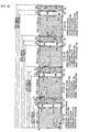
- Fig. 4 is an explanatory diagram showing an example in which samples constituting a frame of a 4kx2k signal are mapped into first to fourth sub-images by the mapping unit 11.
- the mapping unit 11 thins out pixel samples, which are extracted from each frame of an input video signal, in units of predetermined samples. In this example, two adjoining samples on the same line are thinned out.
- the mapping unit 11 fetches the thinned out samples in even order frame by frame, and maps them into active periods of the first, second, third, and fourth sub-images conformable to the HD-SDI format.
- the mapping unit 11 maps two samples on an odd-numbered line in each of frames alternately to the first sub-image and second sub-image, and maps two samples on an even-numbered line in each of the frames alternately to the third sub-image and fourth sub-image.
- samples constituting one frame of a 2k ⁇ 1k signal are mapped into the first to fourth sub-images that is arisen in the active period defined in the HD-SDI format.
- mapping unit 11 separates each of the mapped first, second, third, and fourth sub-images into a first-link transmission channel (LinkA) and a second-link transmission channel (LinkB), and thus maps the sub-images to eight channels.
- LinkA first-link transmission channel
- LinkB second-link transmission channel
- the mapping unit 11 is a circuit that maps a frame, which is formed with a 3840 ⁇ 2160/24P, 25P, 30P/4:4:4, 4:2:2, 4:2:0/10, 12-bit image signal, into HD-SDI signals on channels CH1 to CH8 (eight channels of channels CH1, CH3, CH5, and CH7 belonging to a link LinkA, and channels CH2, CH4, CH6, and CH8 belonging to a link LinkB), which permit a bit rate of 1.485 Gbps or 1.485 Gbps/1.001 (hereinafter, simply, 1.485 Gbps), in conformity with the SMPTE435.
- the mapping unit 11 in this example maps an image signal, which is extracted from a frame formed with 3840 samples and 2160 lines, into first to fourth sub-images, and maps the image signal, which is mapped into the first to fourth sub-images, into HD-SDI signals on eight channels CH1 to CH8 permitting a bit rate of 1.485 Gbps.
- a frame formed with a 4kx2k signal includes multiple samples.
- the position of each of samples in a frame is expressed as (sample number, line number) .
- a first sample group 51 including two adjoining samples at positions (0,0) and (1,0) on the 0th line is mapped into positions (0,42) and (1,42) in the first sub-image and indicated as a first sample group 51'.
- a second sample group 52 including two adjoining samples at positions (2,0) and (3,0) on the 0th line is mapped into positions (0,42) and (1,42) in the second sub-image and indicated as a second sample group 52'.
- a third sample group 53 including two adjoining samples at positions (0,1) and (1,1) on the first line is mapped into positions (0,42) and (1,42) in the third sub-image and indicated as a third sample group 53'.
- a fourth sample group 54 including two adjoining samples at positions (2,1) and (3,1) on the first line is mapped into positions (0,42) and (1,42) in the fourth sub-image and indicated as a fourth sample group 54'.
- i, 2i, and 2i-1 values are assigned in a line direction, and j, 2j, and 2j-1 values are assigned in a sample direction.
- i values are assigned in the line direction, and j values are assigned in the sample direction.
- the mapping unit 11 maps a first sample group, which is located at the 2j-1-th (where j denotes a natural number) sample group position on the 2i-1-th (where i denotes a natural number) line in a frame, into the j-th sample group position on the i-th line in the first sub-image.
- the mapping unit 11 maps a second sample group, which is located at the 2j-th sample group position on the 2i-1-th line in the frame, into the j-th sample group position on the i-th line in the second sub-image.
- the mapping unit 11 maps a third sample group, which is located at the 2j-1-th sample group position on the 2i-th line in the frame, into the j-th sample group position on the i-th line in the third sub-image.
- the mapping unit 11 maps a fourth sample group, which is located at the 2j-th sample group position on the 2i-th line in the frame, into the j-th sample group position on the i-th line in the fourth sub-image.
- a frame is constructed according to any of the RGB,YCbCr/4:4:4 mode, YCbCr/4:2:2 mode, or YCbCr/4:2:0 mode. If a frame can be transmitted over a single HD-SDI cable, no problem would occur. However, since an amount of data increases, it is impossible to transmit the frame over the single HD-SDI cable. Therefore, samples of the frame (information including an image signal) are appropriately extracted and transmitted in the form of multiple sub-images.
- odd-numbered samples contain only information Y on a luminance signal. Further, only the information Y on the luminance signal is contained in odd-numbered lines. Therefore, each of the odd-numbered samples is mapped together with an adjoining even-numbered sample (including CbCr) into a sub-image. Thus, an image can be reproduced directly from the sub-image, though the resolution of the original image of the frame is degraded. Only the information Y on the luminance signal is contained in the third and fourth sub-images. For checking an image to be reproduced, an image representing luminance values alone poses no problem.
- a frame When samples are mapped into the first to fourth sub-images, a frame can be transmitted over a dual link (two HD-SDI cables). Therefore, the samples mapped into the first to fourth sub-images can be transmitted over a total of eight HD-SDI cables.
- Fig. 6 shows an example in which the first to fourth sub-images into which samples are mapped are mapped into channels classified into links LinkA and LinkB.
- the SMPTE435 is a 10G interface standard signifying that HD-SDI signals placed on multiple channels are 8B/10B-encoded in units of two samples (40 bits), thus converted into 50-bit signals, multiplexed channel by channel, and then serially transmitted at a bit rate of 10.692 Gbps or 10.692 Gbps/1.001 (hereinafter, simply, 10.692 Gbps).
- a technology for mapping a 4kx2k signal into the HD-SDI signals is stipulated in Figure 3 and Figure 4 in 5.4 Octa Link 1.5 Gbps Class of Part 1 of the SMPTE435.
- signals on channels CH1(LinkA) and CH2(LinkB), signals on channels CH3(LinkA) and CH4(LinkB), signals on channels CH5(LinkA) and CH6(LinkB), and signals on channels CH7(LinkA) and CH8(LinkB) are constructed in conformity with the SMPTE372M (dual link).
- the mapping unit 11 in accordance with the present embodiment thins a 3840 ⁇ 2160/24P, 25P, 30P/4:4:4, 4:2:2, 4:2:0/10, 12-bit signal in units of two samples in a line direction to obtain one sample, and multiplexes the obtained sample into an active period of an HD-SDI signal. Since each sample can be mapped to a 1920 ⁇ 1080/24P, 25P, 30P/4:4:4, 4:2:2, 4:2:0/10, 12-bit signal on each of four channels, the resultant signals can be transmitted over existing HD-SDI dual-link cables. Further, the signals can be multiplexed and transmitted at 10.692 Gb/s.
- a 4:2:0 signal can be treated as a signal equivalent to a 4:2:2 signal.
- the link LinkB is not used but only the link LinkA including four channels is used. Talking of a 10.692 Gb/s serial interface, the channel CH1 is needed for clock synchronization.
- D0.0 is embedded in signals on the channels CH2 to CH8.
- Mapped HD-SDI signals on eight channels are equivalent to "a Quad link 292 comparable to a 1920 ⁇ 1080/50P, 60P/4:4:4, 4:2:2, 4:2:0/12-bit signal ⁇ 2 channels".
- Fig. 7A and Fig. 7B schematically show the data structures.
- Fig. 7A on the link LinkA, one sample is 20 bits long, and all the bits represent R, G, or B values. Even on the link LinkB, as shown in Fig. 7A , one sample is 20 bits long.
- Fig. 7B out of 10 bits R'G'B'n:0-1, six bits of bit numbers 2 to 7 represent R, G, or B values. Therefore, the number of bits representing R, G, or B values in one sample is 16.
- the HD-SDI signals on the channels CH1 to CH8 mapped as mentioned above by the mapping unit 11 are, as shown in Fig. 2 , transmitted to an S/P-scrambling-8B/10B unit 12.
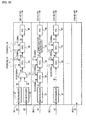
- Fig. 8 is a block diagram showing the constitution of the S/P-scrambling-8B/10B unit 12.
- the S/P-scrambling-8B/10B unit 12 includes eight blocks 12-1 to 12-8 associated on one-to-one basis with the channels CH1 to CH8.
- the constitution of the block 12-1 is different from those of the blocks 12-3, 12-5, and 12-7.
- the blocks 12-3, 12-5, and 12-7 share the same constitution (in the drawing, the constitution of the block 12-3 is shown but the constitutions of the blocks 12-5 and 12-7 are not shown).
- the blocks 12-2, 12-4, 12-6, and 12-8 for the channels CH2, CH4, CH6, and CH8 belonging to the link LinkB share the same constitution (in the drawing, the constitution of the block 12-2 is shown but the constitutions of the blocks 12-4, 12-6, and 12-8 are not shown).
- the same reference numerals are assigned to components that perform pieces of identical processing.
- the blocks 12-1, 12-3, 12-5, and 12-7 for the link LinkA will be described.
- inputted HD-SDI signals on the channels CH1, CH3, CH5, and CH7 are transferred to serial-to-parallel (S/P) converters 21.
- S/P converter 21 serial-to-parallel converts the HD-SDI signal into parallel digital data of 20 bits wide to be transmitted at a bit rate of 74.25 Mbps or 74.25 Mops/1.001 (hereinafter, simply, 74.25 Mbps), and extracts a clock of 74.25 MHz.
- Parallel digital data serial-to-parallel converted by the S/P converter 21 is transmitted to a TRS detector 22.
- a clock of 74.25 MHz extracted by the S/P converter 21 is transmitted as a writing clock to a FIFO memory 23.
- the clock of 74.25 MHz extracted by the S/P converter 21 in the block 12-1 is also transmitted to a phase locked loop (PLL) 13 shown in Fig. 2 .
- PLL phase locked loop
- the TRS detector 22 detects timing reference signals SAV and EAV from a parallel digital video signal sent from the S/P converter 21, and establishes bit synchronization and word synchronization on the basis of the result of the detection.
- Parallel digital data having undergone processing of the TRS detector 22 is transmitted to the FIFO memory 23, and written in the FIFO memory 23 responsively to the clock of 74.25 MHz sent from the S/P converter 21.
- the PLL 13 in Fig. 2 transmits as a reading clock a clock of 37.125 MHz, which is produced by halving the frequency of the clock of 74.25 MHz sent from the S/P converter 21 in the block 12-1, to the FIFO memories 23 in the respective blocks 12-1 to 12-8, and transmits the clock as a writing clock to FIFO memories 26 in the respective blocks 12-1 to 12-8 and a FIFO memory 27 in the block 12-1.
- the PLL 13 transmits as a reading clock a clock of 83. 5312 MHz, which is produced by multiplying the frequency of the clock of 74.25 MHz sent from the S/P converter 21 in the block 12-1 by 9/8, to the FIFO memories 26 in the respective blocks 12-1 to 12-8 and the FIFO memory 27 in the block 12-1, and also transmits the clock as a writing clock to the FIFO memory 16 shown in Fig. 2 .
- the PLL 13 transmits as a reading clock a clock of 167.0625 MHz, which is produced by multiplying the frequency of the clock of 74.25 MHz sent from the S/P converter 21 in the block 12-1 by 9/4, to the FIFO memory 16 shown in Fig. 2 .
- the PLL 13 transmits as a reading clock a clock of 668.25 MHz, which is produced by multiplying the frequency of the clock of 74.25 MHz sent from the S/P converter 21 in the block 12-1 by 9, to a multi-channel data construction unit 17 shown in Fig. 2 .
- parallel digital data of 20 bits wide written responsively to the clock of 74.25 MHz sent from the S/P converter 21 is read from the FIFO memory 23 as parallel digital data of 40 bits wide in units of two samples responsively to the clock of 37.125 MHz sent from the PLL 13 in Fig. 2 , and transmitted to a scrambler 24.
- the parallel digital data of 40 bits wide read from the FIFO memory 23 is also transmitted to an 8B/10B encoder 25.
- the scrambler 24 is a self-synchronous scrambler.
- a self-synchronous scrambling method is a scrambling method adopted in the SMPTE292M, and is such that: a transmitting side regards an inputted serial signal as a polynomial expression, sequentially divides the polynomial expression by a nine-degree primitive polynomial expression X 9 +X 4 +1, transmits the result of the division or the quotient, and thus statistically averagely halves the mark ratio (ratio of 1s to 0s) of transmission data.
- the scrambling has the meaning of encryption of a signal using a primitive polynomial expression.
- the quotient is divided by X+1, whereby polarity-free data (data and reverse data have the same information) is transmitted.
- an original serial signal is reproduced by performing the processing (descrambling) of multiplying a received serial signal by X+1 and further multiplying the resultant signal by the primitive polynomial expression X 9 +X 4 +1.
- the scrambler 24 does not scramble all data items on each horizontal line but scrambles only a timing reference signal SAV, an active line, a timing reference signal EAV, a line number LN, and an error detection code CRC.
- the scrambler 24 does not scramble data of a horizontal blanking period. Immediately previously to the timing reference signal SAV, all the values in a register in the scrambler are set to 0s, and encoding is carried out. Data of up to 10 bits long succeeding the error detection code CRC is outputted.
- the descrambler on the receiving side reproduces data
- the descrambler miscalculates or incorrectly carries the last several bits of a CRC.
- the error detection code CRC is therefore not accurately reproduced.
- a clock for a scrambler is stopped during a horizontal blanking interval, during which no data is transmitted, so that the CRC can be accurately reproduced.
- the subsequent timing reference signal SAV is needed during calculation of the CRC. This poses a problem in that timing control becomes hard to do.
- timing reference signal SAV Only data items of a timing reference signal SAV, an active line, a timing reference signal EAV, a line number LN, and an error detection code CRC are therefore scrambled.
- all the values in a register in the scrambler 24 are set to 0s, and encoding is carried out. Data of at least several bits (for example, 10 bits) long succeeding the error detection code CRC is outputted.
- a pathological pattern is not generated in scrambled data.
- the pathological pattern is generation of a signal exhibiting a pattern (or a reverse pattern) that has, as shown in Fig. 9A , "H" of one bit succeeded by continuation of "L” over nineteen bits, or generation of a signal exhibiting a pattern (or a reverse pattern) that has, as shown in Fig. 9B , continuation of "H” over twenty bits succeeded by continuation of "L” over twenty bits, along one horizontal line on a serial transmission path when data is subjected to self-synchronous scrambling.
- the pattern shown in Fig. 9A and the reverse pattern are patterns having a dc component as a majority.
- an ac-coupled transmission system is generally employed.
- the ac-coupled transmission system when the dc component occupies the majority, a warp of a base line like the one shown in Fig. 10 takes place. Therefore, an apparatus on a receiving side has to reproduce the dc component.
- the pattern shown in Fig. 9B and the reverse pattern are patterns in which a transition from 0 to 1 or from 1 to 0 hardly occurs.
- a receiving apparatus therefore has difficulty in reproducing a clock from a serial signal.
- two low-order bits of XYZ that is the last word in the timing reference signal SAV may be set to 0s.
- the scrambler 24 in the block 12-1 performs scrambling with the two low-order bits set to 0s.
- the scrambler 24 in the block 12-3 performs scrambling after rewriting the two low-order bits to 0 and 1 respectively.
- the scrambler 24 in the block 12-5 performs scrambling after rewriting the two low-order bits into 1 and 0 respectively.
- the scrambler 24 in the block 12-7 performs scrambling after rewriting the two low-order bits to 1s.
- scrambling is performed with the values of the two low-order bits varied among the channels CH1, CH3, CH5, and CH7.
- Parallel digital data of 40 bits wide scrambled by the scrambler 24 as mentioned above is written in the FIFO memory 26 responsively to the clock of 37.125 MHz sent from the PLL 13 shown in Fig. 2 . Thereafter, the parallel digital data is read from the FIFO memory 26 responsively to the clock of 83.5312 MHz sent from the PLL 13 while having the width of 40 bits left intact, and then transmitted to a multiplexing unit 14 shown in Fig. 2 .
- the 8B/10B encoder 25 in the block 12-1 8-bit-to-10-bit encodes data of a horizontal blanking period alone out of parallel digital data of 40 bits wide read from the FIFO memory 23.
- Parallel digital data of 50 bits wide having been 8-bit-to-10-bit encoded by the 8B/10B encoder 25 is written in the FIFO memory 27 responsively to the clock of 37.125 MHz sent from the PLL 13 in Fig. 2 . Thereafter, the parallel digital data is read from the FIFO memory 27 responsively to the clock of 83.5312 MHz sent from the PLL 13 while having the width of 50 bits left intact, and transmitted to the multiplexing unit 14 shown in Fig. 2 .
- Data of a horizontal blanking period is transmitted from the block 12-1 alone (that is, data on the channel CH1 is transmitted) to the multiplexing unit 14, but data items of horizontal blanking periods (on the channels CH3, CH5, and CH7) are not transmitted from the respective blocks 12-3, 12-5, and 12-7 to the multiplexing unit 14. This is because of the restrictions imposed on an amount of data.
- the extractor 28 is a circuit that extracts bits of R, G, and B values (sixteen bits representing R, G, and B values out of twenty bits constituting one sample on the link LinkB shown in Fig. 7B ) from only data items of a timing reference signal SAV, an active line, a timing reference signal EAV, a line number LN, and an error detection code CRC out of all data items on each horizontal line on the link LinkB.
- Parallel digital data of 16 bits wide extracted by the extractor 28 is written in the FIFO memory 23 responsively to the clock of 74.25 MHz sent from the S/P converter 21. Thereafter, the parallel digital data is read as parallel digital data of 32 bits wide in units of two samples responsively to the clock of 37.125 MHz sent from the PLL 13 in Fig. 2 , and transmitted to a K28.5 inserter 29.
- the K28.5 inserter 29 inserts 8-bit word data to the leading part of the timing reference signal SAV or EAV.
- the 8-bit word data is converted into 10-bit word data (called a code name of K28.5), which is not used as word data representing a video signal, during 8-bit-to-10-bit encoding.
- Parallel digital data of 32 bits wide having undergone the processing of the K28.5 inserter 29 is transmitted to an 8B/10B encoder 30.
- the 8B/10B encoder 30 8-bit-to-10-bit encodes the parallel digital data of 32 bits wide, and outputs the resultant data.
- Parallel digital data of 40 bits wide 8-bit-to-10-bit encoded by the 8B/10B encoder 30 is written in the FIFO memory 26 responsively to the clock of 37.125 MHz sent from the PLL 13 in Fig. 2 . Thereafter, the parallel digital data is read from the FIFO memory 26 responsively to the clock of 83.5312 MHz sent from the PLL 13 while having the width of 40 bits left intact, and transmitted to the multiplexing unit 14 shown in Fig. 2 .
- the multiplexing unit 14 shown in Fig. 2 multiplexes parallel digital data items of 40 bits wide on the channels CH1 to CH8 (data items of only a timing reference signal SAV, an active line, a timing reference signal EAV, a line number LN, and an error detection code CRC), which are read from the FIFO memories 26 in the respective blocks 12-1 to 12-8 in the S/P-scrambling-8B/10B unit 12, in units of 40 bits in the order of the channel CH2 (channel whose data is 8-bit-to-10-bit encoded), the channel CH1 (channel whose data is subjected to self-synchronous scrambling), the channel CH4 (channel whose data is 8-bit-to-10-bit encoded), the channel CH3 (channel whose data is subjected to self-synchronous scrambling), the channel CH6 (channel whose data is 8-bit-to-10-bit encoded), the channel CH5 (channel whose data is subjected to self-synchronous scrambling), the channel CH8 (channel whose data is 8-
- Data 8-bit-to-10-bit encoded is inserted to data, which is subjected to self-synchronous scrambling, in units of 40 bits. Therefore, a variation in a mark ratio (a ratio of 0s to 1s) dependent on a scrambling method and unstableness in a transition from 0 to 1 or from 1 to 0 are resolved. Eventually, occurrence of the aforesaid pathological pattern can be prevented.
- the multiplexing unit 14 multiplexes, as shown in Fig. 12B , parallel digital data items of 50 bits wide of four samples, which are contained in only a horizontal blanking period of data on the channel CH1 and are read from the FIFO memory 27 in the block 12-1 in the S/P-scrambling-8B/10B unit 12, so as to produce data of 200 bits wide.
- Parallel digital data of 320 bits wide and parallel digital data of 200 bits wide which result from multiplexing performed by the multiplexing unit 14 are transmitted to a data length conversion unit 15.
- the data length conversion unit 15 is formed using a shift register. Data of 256 bits wide into which the parallel digital data of 320 bits wide is converted, and data of 256 bits wide into which the parallel digital data of 200 bits wide is converted are used to construct parallel digital data of 256 bits wide.
- the parallel digital data of 256 bits wide is further converted into data of 128 bits wide.
- Fig. 13 to Fig. 15 are diagrams showing the structures of parallel digital data of 256 bits wide constructed by the data length conversion unit 15.
- Fig. 13 shows the data structure for one line in the 30P mode.
- Fig. 14 shows the data structure for one line in the 25P mode.
- Fig. 15 shows the data structures for four lines in the 24P mode (since the number of bits of the last word becomes 128 in cycles of four lines in the 24P mode, the data structures for four lines are depicted).
- a frame rate and the number of lines are identical to those of an HD-SDI signal on the channel CH1.
- the S/P-scrambling-8B/10B unit 12 adopts both scrambling and 8B/10B encoding, and performs scrambling on data on the channel CH1 (scrambling adopted by the SMPTE292M). Therefore, the data structures shown in Fig. 13 to Fig. 15 are basically identical to those for the HD-SDI signal.
- data on one line includes three fields mentioned below.
- parallel digital data converted into data of 128 bits wide by the data length conversion unit 15 is transmitted to a FIFO memory 16, and written in the FIFO memory 16 responsively to a clock of 83.5312 MHz sent from the PLL 13.
- Parallel digital data of 128 bits wide written in the FIFO memory 16 is read from the FIFO memory 16 as parallel digital data of 64 bits wide responsively to a clock of 167. 0625 MHz sent from the PLL 13 in Fig. 2 , and transmitted to a multi-channel data construction unit 17.
- the multi-channel data construction unit 17 is, for example, a ten gigabit-sixteen bit interface (XSBI) (16-bit interface to be used in a 10-gigabit Ethernet (Ethernet is a registered trademark) system).
- the multi-channel data construction unit 17 uses a clock of 668.25 MHz sent from the PLL 13 to construct serial digital data items on sixteen channels, which permit a bit rate of 668.25 Mbps, from parallel digital data of 64 bits wide read from the FIFO memory 16.
- the serial digital data items on sixteen channels constructed by the multi-channel data construction unit 17 are transmitted to a multiplexing-P/S conversion unit 18.
- the multiplexing-P/S conversion unit 18 in this example has the capability of a parallel-to-serial conversion unit that serially converts first, second, third, and fourth sub-images mapped by the mapping unit 11.
- Fig. 16A, Fig. 16B, and Fig. 16C are diagrams showing data structures for one line in serial digital data permitting 10.692 Gbps.
- Fig. 16A shows the structure in the 24P mode
- Fig. 16B shows the structure in the 25P mode
- Fig. 16C shows the structure in the 30P mode.
- SAV, an active line, and EAV are shown as data items including a line number LN and an error detection code CRC.
- a horizontal blanking period is shown to include a field of appended data shown in Fig. 13 to Fig. 15 .
- the numbers of bits of a horizontal blanking period specified in the SMPTE435, that is, 86880 bits, 71040 bits, and 7680 bits are larger than the numbers of bits of data on the channel CH1 ⁇ data of the horizontal blanking period - (data items of the timing reference signal SAV, timing reference signal EAV, line number LN, and error detection code CRC) ⁇ , that is, 20450 bits, 17700 bits, and 6700 bits respectively. Therefore, the data of the horizontal blanking period on the channel CH1 can be multiplexed.
- serial digital data that is produced by the multiplexing-P/S conversion unit 18 and permits a bit rate of 10.692 Gbps is transmitted to a photoelectric conversion unit 19.
- the photoelectric conversion unit 19 functions as an output unit that outputs the serial digital data, which permits the bit rate of 10.692 Gbps, to the CCU 2.
- the serial digital data that permits the bit rate of 10.692 Gbps and is converted into a light signal by the photoelectric conversion unit 19 is transmitted from the broadcasting camera 1 to the CCU 2 over the optical fiber cable 3 shown in Fig. 1 .
- signal processing to be performed on a side of transmitting a 3840 ⁇ 2160/24P, 25P, 30P/4:4:4, 4:2:2, 4:2:0/10, 12-bit signal as serial digital data can be carried out.
- 12-bit signal is mapped into HD-SDI signals on the channels CH1 to CH8 (channels CH1, CH3, CH5, and CH7 belonging to the link LinkA, and channels CH2, CH4, CH7, and CH8 belonging to the link LinkB), the HD-SDI signals are serial-to-parallel converted.
- the signals on the link LinkA are subjected to self-synchronous scrambling, and the signals on the link LinkB have the R, G, and B bits thereof 8-bit-to-10-bit encoded.
- self-synchronous scrambling is not performed on all data items on each horizontal line but is performed on only data items of the timing reference signal SAV, active line, timing reference signal EAV, line number LN, and error detection code CRC.
- the self-synchronous scrambling is not performed on data of the horizontal blanking period. All the values in the register in the scrambler are set to 0s immediately previously to the timing reference signal SAV, and encoding is carried out. Data of at least several bits succeeding the error detection code CRC is outputted.
- the descrambler on the receiving side reproduces data
- the descrambler miscalculates or incorrectly carries the last several bits of a CRC.
- the error detection code CRC is therefore not accurately reproduced.
- the calculation of the CRC requires the subsequent timing reference signal SAV. This poses a problem in that timing control becomes hard to do.
- all the values in the register in the descrambler are set to 0s immediately previously to the timing reference signal SAV, and decoding is initiated.
- data of at least several bits long succeeding the error detection code CRC is descrambled. Therefore, calculation can be performed accurately in consideration of carrying by the descrambler serving as a multiplication circuit in order to reproduce original data.
- R, G, and B bits are extracted from only the data items of the timing reference signal SAV, active line, timing reference signal EAV, line number LN, and error detection code CRC among all data items on each horizontal line.
- the R, G, and B bits are 8-bit-to-10-bit encoded.
- the data items on the link LinkA having undergone self-synchronous scrambling and the data items on the link LinkB having been 8-bit-to-10-bit encoded are multiplexed. Serial digital data permitting a bit rate of 10.692 Gbps is produced from the multiplexed parallel digital data items.
- Fig. 17 is a block diagram showing a portion relating to the present embodiment in the circuitry of the CCU 2.
- the CCU 2 multiple sets of circuits like those shown in Fig. 17 are included in one-to-one association with broadcasting cameras 1.
- Serial digital data that is transmitted from the broadcasting camera 1 over the optical fiber cable 3 and permits a bit rate of 10. 692 Gbps is converted into an electrical signal by a photoelectric conversion unit 31, and then transmitted to a S/P conversion-multi-channel data construction unit 32.
- the S/P conversion-multi-channel data construction unit 32 is, for example, the aforesaid XSBI.
- the S/P conversion-multi-channel data construction unit 32 receives first, second, third, and fourth sub-images into which a video signal is mapped and each of which is separated into a first-link channel and a second-link channel.
- the S/P conversion-multi-channel data construction unit 32 serial-to-parallel converts serial digital data that permits a bit rate of 10.692 Gbps, constructs serial digital data items on sixteen channels, which permit a bit rate of 668.25 Mbps, from parallel digital data resulting from the serial-to-parallel conversion, and extracts a clock of 668.25 MHz.
- Parallel digital data items on sixteen channels constructed by the S/P conversion-multi-channel data construction unit 32 are transmitted to a multiplexing unit 33.
- a clock of 668.25 MHz extracted by the S/P conversion-multi-channel data construction unit 32 is transmitted to a PLL 34.
- the multiplexing unit 33 multiplexes serial digital data items on sixteen channels sent from the S/P conversion-multi-channel data construction unit 32, and transmits parallel digital data of 64 bits wide to a FIFO memory 35.
- the PLL 34 transmits a clock of 167.0625 MHz, which has a quarter of the frequency of the clock of 668.25 MHz sent from the S/P conversion-multi-channel data construction unit 32, as a writing clock to the FIFO memory 35.
- the PLL 34 transmits a clock of 83.5312 MHz, which has a one-eighth of the frequency of the clock of 668.25 MHz sent from the S/P conversion-multi-channel data construction unit 32, as a reading clock to the FIFO memory 35, and transmits the clock as a writing clock to a FIFO memory 44 incorporated in a descrambling-8B/10B-P/S unit 38 that will be described later.
- the PLL 34 transmits a clock of 37.125 MHz, which has a one-eighteenth of the frequency of the clock of 668.25 MHz sent from the S/P conversion-multi-channel data construction unit 32, as a reading clock to the FIFO memory 44 and transmits the clock to the FIFO memory 45 incorporated in the descrambling-8B/10B-P/S unit 38, as a writing clock.
- the PLL 34 transmits a clock of 74.25 MHz, which has a one-ninth of the frequency of the clock of 668.25 MHz sent from the S/P conversion-multi-channel data construction unit 32, as a reading clock to the FIFO memory 45 in the descrambling-8B/10B-P/S unit 38.
- parallel digital data of 64 bits wide sent from the multiplexing unit 33 is written responsively to the clock of 167. 0625 MHz sent from the PLL 34.
- the parallel digital data written in the FIFO memory 35 is read as parallel digital data of 128 bits wide responsively to the clock of 83.5312 MHz sent from the PLL 34, and transmitted to a data length conversion unit 36.
- the data length conversion unit 36 is formed using a shift register, and converts parallel digital data of 128 bits wide into data of 256 bits wide (data having the structure shown in any of Fig. 13 to Fig. 15 ).
- the data length conversion unit 36 detects K28. 5 inserted into each of timing reference signals SAV or EAV so as to discriminate line periods from one another, converts sets of data items of the timing reference signal SAV, active line, timing reference signal EAV, line number LN, and error detection code CRC into data of 320 bits wide, and converts data of a horizontal blanking period (as mentioned previously, data of a horizontal blanking period on a channel CH1 having been 8B/10B encoded) into data of 200 bits wide. Appended data shown in Fig. 13 to Fig. 15 is discarded.
- Parallel digital data of 320 bits wide and parallel digital data of 200 bits wide that have the data lengths thereof converted by the data length conversion unit 36 are transmitted to a separation unit 37.
- the separation unit 37 separates parallel digital data of 320 bits wide, which is sent from the data length conversion unit 36 (sets of data items of the timing reference signal SAV, active line, timing reference signal EAV, line number LN, and error detection code CRC), into data items on channels CH1 to CH8 (see Fig. 12A ) that are 40-bit data items identical to data items which are not multiplexed by the multiplexing unit 14 ( Fig. 2 ) included in the broadcasting camera 1.
- the parallel digital data items of 40 bits wide on the channels CH1 to CH8 are transmitted to the descrambling-8B/10B-P/S unit 38.
- the separation unit 37 separates parallel digital data of 200 bits wide, which is sent from the data length conversion unit 36 (data of a horizontal blanking period on a channel CH1 having been 8B/10B encoded), into 50-bit data items (see Fig. 12B ) identical to data items that have not been multiplexed by the multiplexing unit 14.
- the parallel digital data items of 50 bits wide are transmitted to the descrambling-8B/10B-P/S unit 38.
- Fig. 18 is a block diagram showing the constitution of the descrambling-8B/10B-P/S unit 38.
- the descrambling-8B/10B-P/S unit 38 includes eight blocks 38-1 to 38-8 associated on a one-to-one basis with the channels CH1 to CH8.
- the descrambling-8B/10B-P/S unit 38 functions as a receiving unit that receives first, second, third, and fourth sub-images into which an image signal is mapped and each of which is divided into a first-link channel and a second-link channel.
- the block 38-1 has a different constitution from the other blocks 38-3, 38-5, and 38-7 do.
- the blocks 38-3, 38-5, and 38-7 share the same constitution (in the drawing, the constitution of the block 38-3 is shown but the constitutions of the blocks 38-5 and 38-7 are not shown).
- the blocks 38-2, 38-4, 38-6, and 38-8 for the channels CH2, CH4, CH6, and CH8 belonging to a link LinkB share the same constitution (in the drawing, the constitution of the block 38-2 is shown but the constitutions of the blocks 38-4, 38-6, and 38-8 are not shown).
- the same reference numerals are assigned to components that perform pieces of identical processing.
- the descrambler 41 is a self-synchronous descrambler.
- the descrambler 41 descrambles received parallel digital data, sets all the values in a register in the descrambler 41 to 0s immediately previously to the timing reference signal SAV, and then initiates decoding.
- the descrambler 41 performs self-synchronous descrambling on data of 10 bits long succeeding the error detection code CRC.
- the descrambler 41 After performing self-synchronous scrambling, the descrambler 41 changes the values of two low-order bits of XYZ contained in the timing reference signal SAV (bits scrambled with the values thereof varied among the channels CH1, CH3, CH5, and CH7 as described in relation to the scrambler 24) into 0s that are their original values.
- Parallel digital data of 40 bits wide descrambled by the descrambler 41 in the block 38-1 is transmitted to a selector 43.
- inputted parallel digital data of 50 bits wide (data of the horizontal blanking period on the channel CH1 having been 8B/10B encoded) is transmitted to an 8B/10B decoder 42.
- the 8B/10B decoder 42 8-bit-to-10-bit decodes the parallel digital data.
- the parallel digital data of 40 bits wide 8-bit-to-10-bit decoded by the 8B/10B decoder 42 is transmitted to the selector 43.
- the selector 43 alternately selects parallel digital data sent from the descrambler 41 and parallel digital data sent from the 8B/10B decoder 42, constructs parallel digital data of 40 bits wide into which all data items on each horizontal line are integrated, and transmits the parallel digital data of 40 bits wide to a FIFO memory 44.
- Parallel digital data of 40 bits wide sent to the FIFO memory 44 is written in the FIFO memory 44 responsively to the clock of 83.5312 MHz sent from the PLL 34 ( Fig. 17 ). Thereafter, the parallel digital data is read from the FIFO memory 44 responsively to the clock of 37.125 MHz sent from the PLL 34 while having the width of 40 bits left intact, and then transmitted to a FIFO memory 45.
- Parallel digital data of 40 bits wide sent to the FIFO memory 45 is written in the FIFO memory 45 responsively to the clock of 37.125 MHz sent from the PLL 34 ( Fig. 17 ). Thereafter, the parallel digital data is read from the FIFO memory 45 as parallel digital data of 20 bits wide (data of one sample on the link LinkA shown in Fig. 7 ) responsively to the clock of 74.25 MHz sent from the PLL 34, and transmitted to a parallel-to-serial (P/S) converter 46.
- P/S parallel-to-serial
- the P/S converter 46 parallel-to-serial converts the parallel digital data into an HD-SDI signal permitting a bit rate of 1.485 Gbps so as to reproduce the HD-SDI signal.
- the HD-SDI signals on the channels CH1, CH3, CH5, and CH7 reproduced by the blocks 38-1, 38-3, 38-5, and 38-7 are transmitted to a 4kx2k reproduction unit 39 shown in Fig. 18 .
- the 8B/10B decoder 47 8-bit-to-10-bit decodes the parallel digital data.
- the parallel digital data of 32 bits wide 8-bit-to-10-bit decoded by the 8B/10B decoder 47 is transmitted to the FIFO memory 44.
- Parallel digital data of 32 bits wide sent to the FIFO memory 44 is written in the FIFO memory 44 responsively to the clock of 83.5312 MHz sent from the PLL 34 ( Fig. 17 ). Thereafter, the parallel digital data is read from the FIFO memory 44 responsively to the clock of 37.125 MHz sent from the PLL 34 while having the width of 32 bits left intact, and then transmitted to the FIFO memory 45.
- Parallel digital data of 32 bits wide sent to the FIFO memory 45 is written in the FIFO memory 45 responsively to the clock of 37.125 MHz sent from the PLL 34 ( Fig. 17 ). Thereafter, the parallel digital data is read from the FIFO memory 45 as parallel digital data of 16 bits wide (R, G, and B bits of one sample on the link LinkB shown in Fig. 7 ) responsively to the clock of 74.25 MHz sent from the PLL 34, and then transmitted to a sample data constructor 48.
- the sample data constructor 48 constructs 20-bit data items of samples on the link LinkB to each of which four bits of bit numbers 0, 1, 8, and 9 out of R'G'B'n:0-1 shown in Fig. 7 are appended.
- the thus constructed parallel digital data of 20 bits wide is transmitted from the sample data constructor 48 to the P/S converter 46.
- the P/S converter 46 parallel-to-serial converts the parallel digital data into an HD-SDI signal permitting a bit rate of 1.485 Gbps, and thus reproduces the HD-SDI signal.
- the HD-SDI signals on the channels CH2, CH4, CH6, and CH8 reproduced by the respective blocks 38-2, 38-4, 38-6, and 38-8 are transmitted to the 4kx2k reproduction unit 39 shown in Fig. 18 .
- the 4kx2k reproduction unit 39 shown in Fig. 18 performs processing, which is a reverse of the processing ( Fig. 6 ) of the mapping unit 11 ( Fig. 2 ) of the broadcasting camera 1, on the HD-SDI signals on the channels CH1 to CH8 (links LinkA and LinkB) sent from the S/P-scrambling-8B/10B unit 38.
- the 4kx2k reproduction unit 39 is a circuit that reproduces a 3840 ⁇ 2160/24P,25P,30P/4:4:4,4:2:2,4:2:0/10,12-bit signal through this processing.
- the 4kx2k reproduction unit 39 of this example extracts one by one pixel samples allocated to active periods of first, second, third, and fourth sub-images received by the S/P conversion-multi-channel data construction unit 32.
- the 4kx2k reproduction unit 39 sequentially reallocates the pixel samples to one frame of a video signal, and restores thinned out pixels from the allocated samples.
- the 4kx2k reproduction unit 39 alternately allocates samples, which are mapped to the first and second sub-images, onto odd-numbered lines. Likewise, the 4kx2k reproduction unit 39 alternately allocates samples, which are mapped to the third and fourth sub-images, onto even-numbered lines. The 4kx2k reproduction unit 39 then uses samples, which are allocated to each line, to restore thinned out pixels adjoining the samples.
- a 3840 ⁇ 2160/24P,25P,30P/4:4:4,4:2:2,4:2:0/10,12-bit signal reproduced by the 4kx2k reproduction unit 39 is outputted from the CCU 2, and transmitted to, for example, a VTR or the like (not shown).
- a 3840 ⁇ 2160/24P,25P,30P/4:4:4,4:2:2,4:2:0/10,12-bit signal is transmitted from each broadcasting camera 1 to the CCU 2 but also return video (a video signal to be used to display a picture being picked up by another broadcasting camera 1) is transmitted from the CCU 2 to each broadcasting camera 1 over the optical fiber cable 3.
- the return video is produced using a known technology (for example, after HD-SDI signals on two channels are 8-bit-to-10-bit encoded, the resultant signals are multiplexed and converted into serial digital data). A description of circuitry for the production will be omitted.
- the signal receiving device 6 performs signal processing assigned to a side of receiving serial digital data produced by the signal transmitting device 5.
- parallel digital data is produced from serial digital data permitting a bit rate of 10.692 Gbps, and the parallel digital data is separated into data items on respective channels classified into the links LinkA and LinkB.
- data items of samples on the link LinkB are constructed from 8-bit-to-10-bit decoded R, G, and B bits.
- Parallel digital data on the link LinkA subjected to self-synchronous descrambling and parallel digital data on the link LinkB having samples thereof constructed are parallel-to-serial converted, whereby mapped HD-SDI signals on the channels CH1 to CH8 are reproduced.
- all the values in the register in each of the scramblers 24 are set to 0s immediately previously to the timing reference signal SAV, encoding is carried out, and data of ten bits long succeeding the error detection code CRC is outputted.
- all the values in the register in each of the descramblers 41 are set to 0s immediately previously to the timing reference signal SAV, decoding is initiated, and data of ten bits long succeeding the error detection code CRC is descrambled. Therefore, although data of the horizontal blanking period subjected to self-synchronous scrambling is not transmitted, the CCU 2 that is the receiving side can accurately reproduce original data.
- Scrambling is performed by varying the values of two low-order bits of XYZ in the timing reference signal SAV among the channels belonging to the link LinkA. Therefore, even when a 3840 ⁇ 2160/24P,25P,30P/4:4:4,4:2:2,4:2:0/10,12-bit signal is a flat signal (the R, G, and B values are nearly the same values over an entire screen), an incident that data values become uniform between the channels CH1, CH3, CH5, and CH7 and the channels CH2, CH4, CH6, and CH8 can be avoided. Therefore, occurrence of EMI (Electro-Magnetic Interference) can be prevented.
- EMI Electro-Magnetic Interference
- a 3840 ⁇ 2160/24P,25P,30P/4:4:4,4:2:2,4:2:0/10,12-bit signal is mapped into HD-SDI signals on the channels CH1 to CH8 (links LinkA and LinkB).
- the 3840 ⁇ 2160/24P,25P,30P/4:4:4,4:2:2,4:2:0/10,12-bit signal is converted into serial digital data permitting a bit rate of 10.692 Gbps and transmitted.
- This is advantageous in that a 4k signal can be transmitted through multiple channels supported by a conventionally employed 10.692 Gb/s serial interface.
- a 4kx8k signal representing one frame is extracted in units of two samples and mapped into sub-images.
- Samples mapped into the sub-images are samples constituting one frame that is an original image. Since the sub-images are independently acquired from data of only one channel among data transmitted through multiple channels, a picture on an entire screen can be viewed on an existing HD monitor or a waveform monitor, or an 8k signal can be observed on a 4k monitor or the like. This is advantageous in that an existing HD monitor can be used as a receiving side and it is effective for analysis of a defect in video equipment or the optical fiber cable 3 or the like which is used for transmission.
- a signal is thinned in units of two samples.
- a 3840/60P signal may presumably be changed to 3840/60I signals on two channels through line-by-line thinning, or the 3840/60P signal may presumably be changed to 3840/30P signals on two channels through frame-by-frame thinning.
- an amount of data to be preserved and allocated is small. This is advantageous because a delay time occurring when a signal is transmitted from the broadcasting camera 1 to the CCU 2 is diminished. Performing signal processing that diminishes the delay time has a quite significant meaning for a professional-use camera system requested to carry out signal processing or signal transmission in real time.
- Fig. 19 is an explanatory diagram showing an example in which samples constituting one frame of a 4kx2k signal are mapped into first to fourth sub-images by the mapping unit 11.
- the mapping unit 11 characteristically maps a 3840 ⁇ 2160/50P,60P/4:4:4,4:2:2,4:2:0/10,12-bit signal into the first to fourth sub-images.
- the other components are identical to those of the first embodiment.
- An iterative description will be omitted.
- As for the processing of a signal receiving device 6 included in a CCU 2 since it is identical to that in the first embodiment, an iterative description will be omitted.
- a broadcasting camera 1 in this example is a camera including a signal transmitting device 5 that produces a 3840 ⁇ 2160/50P,60P/4:4:4,4:2:2,4:2:0/10,12-bit signal, which is equivalent to a signal specified in the UHDTV1, as a 4kx2k signal (an untra-high-definition signal representing 4k samples ⁇ 2k lines), and transmits HD-SDI signals into which the signal is mapped according to a predetermined method.
- a signal receiving device 6 included in the CCU 2 in this example can reproduce an image of the 3840 ⁇ 2160/50P,60P/4:4:4,4:2:2,4:2:0/10,12-bit signal, on the basis of the HD-SDI signals received from the broadcasting camera 1.
- the mapping unit 11 in this example is a circuit that maps a 3840 ⁇ 2160/50P,60P/4:4:4,4:2:2,4:2:0/10,12-bit signal into HD-SDI signals on eight channels CH1 to CH8 (channels CH1, CH3, CH5, and CH7 classified into the link LinkA and channels CH2, CH4, CH6, and CH8 classified into the link LinkB), which permit a bit rate of 1.485 Gbps, in conformity with the SMPTE435.
- the mapping unit 11 maps an image signal, which is allocated to a frame, into first to fourth sub-images.
- mapping will be described on the assumption that the position of each of samples included in a frame of a 4kx2k signal and in first to fourth sub-images is expressed as (sample number, line number). For example, two samples at (0,0) and (1,0) in a frame of a 4kx2k signal are mapped to (0,42) and (1,42) in the first sub-image. Two samples at (2,0) and (3,0) in the frame of the 4k ⁇ 2k signal are mapped to (0,42) and (1,42) in the second sub-image.
- the mapping unit 11 thins a 3840 ⁇ 2160/50P,60P/4:4:4,4:2:2,4:2:0/10,12-bit signal in units of two samples in a line direction, and multiplexes the samples to active periods of HD-SDI signals. After mapping samples into 1920 ⁇ 1080/50P,60P/4:4:4,4:2:2,4:2:0/10,12-bit signals on four channels, the mapping unit 11 maps the signals into the links LinkA and LinkB (see Fig. 6 ).
- the broadcasting camera 1 can transmit the signals using a 4-channel Quad link in conformity with the existing HD-SDI.
- the signal can be transmitted through two channels of 10 Gbps.
- signals on two channels of 10G are transmitted over one optical fiber, a 1.3 ⁇ m/1.55 ⁇ m two-wavelength multiplexing technology or a CWDM/DWDM wavelength multiplexing technology can be employed.
- Fig. 20 is an explanatory diagram showing an example in which samples constituting one frame of a 8kx4k signal are mapped into first to fourth sub-images by the mapping unit 11.
- the mapping unit 11 maps a 7680x4320/50P,60P/4:4:4,4:2:2,4:2:0/10,12-bit signal into first to fourth sub-images.
- the other components are identical to those of the first embodiment. Therefore, an iterative description will be omitted.
- a broadcasting camera 1 in this example is a camera including a signal transmitting device 5 that produces a first frame, which is specified with a 7680 ⁇ 4320/50P,60P/4:4:4,4:2:2,4:2:0/10,12-bit signal equivalent to a UHDTV2 signal, as a frame of a 8kx4k signal (an ultra-high-definition signal representing 8k samples ⁇ 4k lines), and transmits HD-SDI signals into which the signal is mapped according to a predetermined method.
- a signal receiving device 6 included in a CCU 2 in this example can reproduce an image of the 7680x4320/50P,60P/4:4:4,4:2:2,4:2:0/10,12-bit signal on the basis of the HD-SD signals received from the broadcasting camera 1.
- the mapping unit 11 in this example is a circuit that maps a 7680x4320/50P,60P/4:4:4,4:2:2,4:2:0/10,12-bit signal into HD-SDI signals on eight channels CH1 to CH8 (channels CH1, CH3, CH5, and CH7 classified into the link LInkA and channels CH2, CH4, CH6, and CH8 classified into the link LinkB), which permit a bit rate of 1.485 Gbps, in conformity with the SMPTE435.
- the 7680x4320/50P,60P/4:4:4,4:2:2,4:2:0/10,12-bit signal is thinned in units of two samples in a line direction, and samples are mapped to the second frame of four channels defined with 3840 ⁇ 2160/50P,60P/4:4:4,4:2:2,4:2:0/10,12-bit signals as shown in Fig. 6 .
- the 3840 ⁇ 2160/50P,60P/4:4:4,4:2:2,4:2:0/10,12-bit signals on four channels are further thinned in units of two samples in the line direction, and samples are mapped to active periods of respective HD-SDI signals.
- the signals are mapped into 1920 ⁇ 1080/50P,60P/4:4:4,4:2:2,4:2:0/10,12-bit signals on four channels, so that the resultant signals can be transmitted through over "a Quad-link 292 conformable to the existing HD-SDI ⁇ four channels".
- the 7680x4320/50P,60P/4:4:4,4:2:2,4:2:0/10,12-bit signal can be mapped to sixteen channels of Quad links. Since "a Quad link 292 ⁇ two channels" can transmit data at 10 Gbps, the data can be transmitted through at eight channels of 10 Gbps.
- CWDM/DWDM Coarse Wavelength Division Multiplexing/Dense Wavelength Division Multiplexing
- the signal when a 7680 ⁇ 4320/50P,60P/4:4:4,4:2:2,4:2:0/10,12-bit signal is mapped into HD-SDI signals on channels CH1 to CH8 (links LinkA and LinkB), the signal can be converted into serial digital data permitting a bit rate of 10.692 Gbps and transmitted.
- This is advantageous in that an 8k signal that is a new-generation video signal deliberated by the ITU or SMPTE can be transmitted using multiple channels supported by a conventionally employed 10.692 Gb/s serial interface.
- Fig. 21 is an explanatory diagram showing an example in which samples constituting one frame of a 4kx2k signal are mapped into first to fourth sub-images by the mapping unit 11.
- the mapping unit 11 maps a 4096x2160/24P/4:4:4/12-bit signal into first to fourth sub-images.
- the other components are identical to those of the first embodiment. Therefore, an iterative description will be omitted.
- processing of a signal receiving device 6 included in a CCU 2 is identical to that in the first embodiment, an iterative description will be omitted.
- a broadcasting camera 1 in this example is a camera including a signal transmitting device 5 that produces a 4096x2160/24P/4:4:4/12-bit signal as a 4kx2k signal (an ultra-high-definition signal representing 4k samples ⁇ 2k lines), and transmits HD-SDI signals into which the signal is mapped according to a predetermined method.
- the signal receiving device 6 included in the CCU 2 in this example can reproduce an image of the 4096x2160/24P/4:4:4/12-bit signal as the 4kx2k signal (an ultra-high-definition signal representing 4k samples ⁇ 2k lines) on the basis of the HD-SDI signals received from the broadcasting camera 1.
- the mapping unit 11 in this example is a circuit that maps a 4096x2160/24P/4:4:4/12-bit signal into HD-SDI signals on eight channels CH1 to CH8 (channels CH1, CH3, CH5, and CH7 classified into a link LinkA and channels CH2, CH4, CH6, and CH8 classified into a link LinkB), which permit a bit rate of 1.485 Gbps, in conformity with the SMPTE435.
- the mapping unit 11 maps an image signal, which is allocated to a frame, into first to fourth sub-images.
- each of positions of samples contained in one frame of a 4kx2k signal and first to fourth sub-images is expressed as (sample number, line number).
- sample number line number
- two samples at (0,0) and (1,0) in one frame of a 4 kx2k signal are mapped into (0,42) and (1,42) respectively in the first sub-image.
- Two samples at (2,0) and (3,0) in the frame of the 4kx2k signal are mapped into (0,42) and (1,42) respectively in the second sub-image.
- the mapping unit 11 thins a 4096x2160/24P/4:4:4/12-bit signal in units of two samples in a line direction, and multiplexes the samples to active periods of HD-SDI signals. After mapping samples into 2048 ⁇ 1080/24P/4:4:4/12-bit signals on four channels, the mapping unit 11 maps the signals into 2048 ⁇ 1080/24P/4:2:2/10-bit signals on the links LinkA and LinkB.
- the broadcasting camera 1 can transmit the signals using eight channels in conformity with the existing HD-SDI.
- the signal can be converted into serial digital data permitting a bit rate of 10.692 Gbps and transmitted.
- This is advantageous in that multiple channels supported by a conventionally employed 10.692 Gb/s serial interface can be used for transmission even in a case where a frame interval is 24P.
- the present invention is applied to a camera transmission system.
- a signal formatted in any of other various modes may be transmitted.
- the present invention can be applied to a case where various signals are transmitted.
- 1 broadcasting camera
- 2 CCU (camera control unit)
- 3 optical fiber cable
- 5 signal transmitting device
- 6 signal receiving device
- 11 mapping unit
- 12 S/P-scrambling-8B/10B unit
- 38-1 to 38-8 blocks of S/P-scrambling-8B/10B unit.
Landscapes
- Engineering & Computer Science (AREA)
- Multimedia (AREA)
- Signal Processing (AREA)
- Television Systems (AREA)
- Two-Way Televisions, Distribution Of Moving Picture Or The Like (AREA)
- Time-Division Multiplex Systems (AREA)
- Studio Devices (AREA)
Applications Claiming Priority (2)
| Application Number | Priority Date | Filing Date | Title |
|---|---|---|---|
| JP2007303628A JP4645638B2 (ja) | 2007-11-22 | 2007-11-22 | 信号送信装置、信号送信方法、信号受信装置及び信号受信方法 |
| PCT/JP2008/070472 WO2009066582A1 (ja) | 2007-11-22 | 2008-11-11 | 信号送信装置、信号送信方法、信号受信装置及び信号受信方法 |
Publications (3)
| Publication Number | Publication Date |
|---|---|
| EP2139236A1 true EP2139236A1 (de) | 2009-12-30 |
| EP2139236A4 EP2139236A4 (de) | 2010-06-23 |
| EP2139236B1 EP2139236B1 (de) | 2017-07-05 |
Family
ID=40667407
Family Applications (1)
| Application Number | Title | Priority Date | Filing Date |
|---|---|---|---|
| EP08852293.3A Not-in-force EP2139236B1 (de) | 2007-11-22 | 2008-11-11 | Signalübertragungsanordnung, signalübertragungsverfahren, signalempfangsanordnung und signalempfangsverfahren |
Country Status (5)
| Country | Link |
|---|---|
| US (1) | US8421915B2 (de) |
| EP (1) | EP2139236B1 (de) |
| JP (1) | JP4645638B2 (de) |
| CN (1) | CN101682739B (de) |
| WO (1) | WO2009066582A1 (de) |
Cited By (3)
| Publication number | Priority date | Publication date | Assignee | Title |
|---|---|---|---|---|
| EP2175637A1 (de) * | 2008-10-09 | 2010-04-14 | Sony Corporation | Signalübertragungsvorrichtung und Signalübertragungsverfahren |
| CN102164285A (zh) * | 2010-02-22 | 2011-08-24 | 索尼公司 | 发送装置、发送方法、接收装置、接收方法和信号传输系统 |
| EP2894862A4 (de) * | 2012-09-04 | 2016-03-23 | Japan Broadcasting Corp | Vorrichtung zum übertragen eines videosignals, vorrichtung zum empfangen eines videosignals, verfahren zum übertragen eines videosignals, verfahren zum empfangen eines videosignals, programm und aufzeichnungsmedium |
Families Citing this family (43)
| Publication number | Priority date | Publication date | Assignee | Title |
|---|---|---|---|---|
| US8347199B2 (en) * | 2009-01-21 | 2013-01-01 | Cisco Technology, Inc. | Enhanced error detection in multilink serdes channels |
| JP5053437B2 (ja) * | 2009-07-10 | 2012-10-17 | 株式会社ナナオ | 信号種別判断装置、及び信号種別判断方法 |
| JP5299165B2 (ja) * | 2009-08-19 | 2013-09-25 | ソニー株式会社 | 信号送信装置、信号送信方法、信号受信装置、信号受信方法、及び信号伝送システム |
| JP5309041B2 (ja) * | 2010-01-07 | 2013-10-09 | 日本放送協会 | インターフェース装置 |
| JP2011146816A (ja) * | 2010-01-12 | 2011-07-28 | Nippon Hoso Kyokai <Nhk> | インターフェース装置 |
| JP2011176635A (ja) * | 2010-02-24 | 2011-09-08 | Sony Corp | 送信装置、送信方法、受信装置、受信方法及び信号伝送システム |
| WO2012157720A1 (ja) | 2011-05-18 | 2012-11-22 | シャープ株式会社 | 液晶パネル、液晶表示装置 |
| JP5870508B2 (ja) * | 2011-05-19 | 2016-03-01 | ソニー株式会社 | 信号送信装置、信号送信方法、信号受信装置、信号受信方法及び信号伝送システム |
| WO2012161188A1 (ja) | 2011-05-25 | 2012-11-29 | シャープ株式会社 | 映像信号処理装置、液晶表示装置 |
| US20140092301A1 (en) * | 2011-05-25 | 2014-04-03 | Sharp Kabushiki Kaisha | Data structure, image transmitting apparatus, image receiving apparatus, display apparatus, image transmitting method, and recording medium |
| JP2012253689A (ja) * | 2011-06-06 | 2012-12-20 | Sony Corp | 信号送信装置、信号送信方法、信号受信装置、信号受信方法及び信号伝送システム |
| US9113020B2 (en) | 2011-07-26 | 2015-08-18 | Lg Electronics Inc. | Apparatus for transmitting video stream, apparatus for receiving video stream, method for transmitting video stream, and method for receiving video stream |
| EP2744197A4 (de) * | 2011-08-11 | 2015-02-18 | Panasonic Corp | Abspielvorrichtung, abspielverfahren, integrierter schaltkreis, rundfunksystem und rundfunkverfahren |
| JP5978574B2 (ja) | 2011-09-12 | 2016-08-24 | ソニー株式会社 | 送信装置、送信方法、受信装置、受信方法および送受信システム |
| JP5232319B2 (ja) | 2011-10-20 | 2013-07-10 | 株式会社東芝 | 通信装置及び通信方法 |
| WO2013094258A1 (ja) * | 2011-12-20 | 2013-06-27 | シャープ株式会社 | 映像出力装置および表示装置 |
| WO2013094259A1 (ja) * | 2011-12-20 | 2013-06-27 | シャープ株式会社 | 表示装置 |
| JP5973766B2 (ja) * | 2012-03-30 | 2016-08-23 | キヤノン株式会社 | 画像処理装置 |
| JP5972016B2 (ja) * | 2012-04-10 | 2016-08-17 | キヤノン株式会社 | 撮像装置 |
| JP6072435B2 (ja) * | 2012-05-29 | 2017-02-01 | シャープ株式会社 | 表示装置、映像出力装置 |
| JP5390667B2 (ja) | 2012-06-11 | 2014-01-15 | 株式会社東芝 | 映像送信機器及び映像受信機器 |
| JP2014003492A (ja) * | 2012-06-19 | 2014-01-09 | Nippon Hoso Kyokai <Nhk> | 送信装置、受信装置及びプログラム |
| US20140085497A1 (en) * | 2012-09-26 | 2014-03-27 | Omnivision Technologies, Inc. | Systems And Methods For Sychronizing Multiple Video Sensors |
| JP2014146924A (ja) * | 2013-01-28 | 2014-08-14 | Sony Corp | ソース機器、シンク機器、通信システムおよび画像送信方法 |
| US9998774B2 (en) | 2013-02-28 | 2018-06-12 | Lg Electronics Inc. | Signal transmission and reception device and signal transmission and reception method |
| CN103152541B (zh) * | 2013-03-11 | 2016-08-17 | 深圳创维-Rgb电子有限公司 | 超高清显示的控制方法及装置、超高清电视机 |
| CN105763888A (zh) * | 2013-05-09 | 2016-07-13 | 蔡留凤 | 可提高电视节目分辨率的超高清数字电视信号发射机 |
| JP2015019182A (ja) | 2013-07-10 | 2015-01-29 | ソニー株式会社 | 信号処理装置、信号処理方法、プログラム、及び、信号伝送システム |
| JP6365899B2 (ja) | 2013-08-22 | 2018-08-01 | ソニー株式会社 | 信号処理装置、信号処理方法、プログラム、及び、信号伝送システム |
| JP6221606B2 (ja) * | 2013-10-08 | 2017-11-01 | ソニー株式会社 | 信号処理装置、信号処理方法、プログラム、及び、信号伝送システム |
| JP6127964B2 (ja) | 2013-12-26 | 2017-05-17 | ソニー株式会社 | 信号切換装置および信号切換装置の動作制御方法 |
| US20180063372A1 (en) * | 2014-11-18 | 2018-03-01 | Elwha Llc | Imaging device and system with edge processing |
| GB201506328D0 (en) * | 2015-04-14 | 2015-05-27 | D3 Technologies Ltd | A system and method for handling video data |
| CN104836974B (zh) | 2015-05-06 | 2019-09-06 | 京东方科技集团股份有限公司 | 视频播放器、显示装置、视频播放系统和视频播放方法 |
| CN105611213A (zh) * | 2016-01-04 | 2016-05-25 | 京东方科技集团股份有限公司 | 一种图像处理方法、播放方法及相关的装置和系统 |
| CN105680871B (zh) * | 2016-04-07 | 2018-09-28 | 武汉芯泰科技有限公司 | 用于数据串行传输的并串、串并转换装置 |
| JP6815181B2 (ja) * | 2016-12-08 | 2021-01-20 | 池上通信機株式会社 | 映像データ伝送処理システム |
| JP6866181B2 (ja) * | 2017-02-24 | 2021-04-28 | キヤノン株式会社 | 画像処理装置、その制御方法、画像処理装置を備える表示装置、プログラム、および記憶媒体 |
| US20180262701A1 (en) * | 2017-03-10 | 2018-09-13 | Raytheon Company | Transporting ultra-high definition video from multiple sources |
| JP6777587B2 (ja) * | 2017-05-11 | 2020-10-28 | 池上通信機株式会社 | 映像出力判定装置、映像出力判定方法及びそれを用いた映像信号スイッチャー |
| US10148381B1 (en) | 2017-06-06 | 2018-12-04 | At&T Intellectual Property I, L.P. | System and method for providing single fiber 4K video |
| US11601254B2 (en) * | 2020-09-18 | 2023-03-07 | Sony Semiconductor Solutions Corporation | Communication apparatus, communications system, and communication method |
| WO2022137325A1 (ja) * | 2020-12-22 | 2022-06-30 | 日本電信電話株式会社 | 映像信号を合成する装置、方法及びプログラム |
Family Cites Families (23)
| Publication number | Priority date | Publication date | Assignee | Title |
|---|---|---|---|---|
| FR1023372A (fr) * | 1950-07-19 | 1953-03-18 | S E D A C Soc | Perfectionnements aux procédés de télévision et dispositifs pour la mise en oeuvre de ces procédés |
| JPS58500635A (ja) * | 1981-04-10 | 1983-04-21 | アムペツクス コ−ポレ−シヨン | 映像を空間的にトランスフオ−ムするシステム |
| US6661463B1 (en) * | 1983-05-09 | 2003-12-09 | David Michael Geshwind | Methods and devices for time-varying selection and arrangement of data points with particular application to the creation of NTSC-compatible HDTV signals |
| US5978035A (en) * | 1983-05-09 | 1999-11-02 | Geshwind; David Michael | Methods and devices for encoding high-definition signals by computing selection algorithms and recording in an off-line manner |
| US4654484A (en) * | 1983-07-21 | 1987-03-31 | Interand Corporation | Video compression/expansion system |
| US4520396A (en) * | 1983-07-25 | 1985-05-28 | Rca Corporation | FM video transmission system having coring and coring compensation for reducing effects of triangular noise |
| US4660096A (en) * | 1984-12-11 | 1987-04-21 | Rca Corporation | Dividing high-resolution-camera video signal response into sub-image blocks individually raster scanned |
| GB2189366B (en) * | 1986-04-17 | 1989-12-28 | British Broadcasting Corp | Method and apparatus for conveying information signals |
| GB2267194B (en) * | 1992-05-13 | 1995-10-04 | Sony Broadcast & Communication | Apparatus and method for processing image data |
| US5430486A (en) * | 1993-08-17 | 1995-07-04 | Rgb Technology | High resolution video image transmission and storage |
| JPH0937241A (ja) * | 1995-07-14 | 1997-02-07 | Nec Eng Ltd | 高能率画像符号化伝送システムとそのエンコーダ装置及びデコーダ装置 |
| CA2243700C (en) * | 1996-11-21 | 2005-04-19 | Philips Electronics N.V. | Transmission and reception of television programs and an additional data service |
| US6038256A (en) * | 1996-12-31 | 2000-03-14 | C-Cube Microsystems Inc. | Statistical multiplexed video encoding using pre-encoding a priori statistics and a priori and a posteriori statistics |
| US6084910A (en) * | 1997-01-31 | 2000-07-04 | Hughes Electronics Corporation | Statistical multiplexer for video signals |
| US6674796B1 (en) * | 2000-02-14 | 2004-01-06 | Harmonic, Inc. | Statistical multiplexed video encoding for diverse video formats |
| US7221406B2 (en) * | 2001-01-30 | 2007-05-22 | Sony Corporation | Data creation method and data transfer method and apparatus |
| US7218751B2 (en) * | 2001-06-29 | 2007-05-15 | Digimarc Corporation | Generating super resolution digital images |
| JP2004088272A (ja) * | 2002-08-26 | 2004-03-18 | Victor Co Of Japan Ltd | 画像伝送システム |
| US7463816B2 (en) * | 2003-09-18 | 2008-12-09 | Cyberlink Corp. | Method of encoding and decoding pictured data for enhancing image resolution |
| JP4114658B2 (ja) | 2004-04-13 | 2008-07-09 | ソニー株式会社 | データ送信装置及びデータ受信装置 |
| JP4760288B2 (ja) * | 2005-10-13 | 2011-08-31 | ソニー株式会社 | 画像表示システム、表示装置、画像再合成装置、画像再合成方法及びプログラム |
| KR100754652B1 (ko) * | 2006-02-09 | 2007-09-05 | 삼성전자주식회사 | 다중 방송 서비스를 제공하기 위한 방송 시스템 및 방법 |
| US7868879B2 (en) * | 2006-05-12 | 2011-01-11 | Doremi Labs, Inc. | Method and apparatus for serving audiovisual content |
-
2007
- 2007-11-22 JP JP2007303628A patent/JP4645638B2/ja not_active Expired - Fee Related
-
2008
- 2008-11-11 WO PCT/JP2008/070472 patent/WO2009066582A1/ja not_active Ceased
- 2008-11-11 US US12/601,126 patent/US8421915B2/en not_active Expired - Fee Related
- 2008-11-11 EP EP08852293.3A patent/EP2139236B1/de not_active Not-in-force
- 2008-11-11 CN CN2008800171614A patent/CN101682739B/zh not_active Expired - Fee Related
Cited By (5)
| Publication number | Priority date | Publication date | Assignee | Title |
|---|---|---|---|---|
| EP2175637A1 (de) * | 2008-10-09 | 2010-04-14 | Sony Corporation | Signalübertragungsvorrichtung und Signalübertragungsverfahren |
| US8396215B2 (en) | 2008-10-09 | 2013-03-12 | Sony Corporation | Signal transmission apparatus and signal transmission method |
| CN102164285A (zh) * | 2010-02-22 | 2011-08-24 | 索尼公司 | 发送装置、发送方法、接收装置、接收方法和信号传输系统 |
| EP2894862A4 (de) * | 2012-09-04 | 2016-03-23 | Japan Broadcasting Corp | Vorrichtung zum übertragen eines videosignals, vorrichtung zum empfangen eines videosignals, verfahren zum übertragen eines videosignals, verfahren zum empfangen eines videosignals, programm und aufzeichnungsmedium |
| US9641875B2 (en) | 2012-09-04 | 2017-05-02 | Nippon Hoso Kyokai | Video signal transmitting device, video signal receiving device, and recording medium |
Also Published As
| Publication number | Publication date |
|---|---|
| WO2009066582A1 (ja) | 2009-05-28 |
| EP2139236A4 (de) | 2010-06-23 |
| CN101682739B (zh) | 2013-01-23 |
| JP2009130639A (ja) | 2009-06-11 |
| CN101682739A (zh) | 2010-03-24 |
| US20100149412A1 (en) | 2010-06-17 |
| EP2139236B1 (de) | 2017-07-05 |
| US8421915B2 (en) | 2013-04-16 |
| JP4645638B2 (ja) | 2011-03-09 |
Similar Documents
| Publication | Publication Date | Title |
|---|---|---|
| EP2139236B1 (de) | Signalübertragungsanordnung, signalübertragungsverfahren, signalempfangsanordnung und signalempfangsverfahren | |
| US8289445B2 (en) | Signal transmitting device and signal transmitting method | |
| JP4692576B2 (ja) | 信号送信装置及び信号送信方法 | |
| US8854540B2 (en) | Signal transmission apparatus, signal transmission method, signal reception apparatus, signal reception method, and signal transmission system | |
| US8982959B2 (en) | Signal transmission apparatus, signal transmission method, signal reception apparatus, signal reception method, and signal transmission system | |
| US9456232B2 (en) | Signal processing apparatus, signal processing method, program, and signal transmission system | |
| US20090213265A1 (en) | Signal inputting apparatus and signal inputting method | |
| US9071375B2 (en) | Signal transmitting apparatus, signal transmitting method, signal receiving apparatus, signal receiving method, and signal transmission system | |
| US20130010187A1 (en) | Signal transmitting device, signal transmitting method, signal receiving device, signal receiving method, and signal transmission system | |
| US8396215B2 (en) | Signal transmission apparatus and signal transmission method | |
| US20110205428A1 (en) | Transmission apparatus, transmission method, reception apparatus, reception method and signal transmission system | |
| AU2014309958B2 (en) | Signal processing device, signal processing method, program, and signal transmission system | |
| CN102821305A (zh) | 信号发送/接收设备和方法以及信号传输系统 | |
| US7477168B2 (en) | Apparatus for and method of processing data | |
| JP4910621B2 (ja) | 信号処理装置及び信号処理方法 |
Legal Events
| Date | Code | Title | Description |
|---|---|---|---|
| PUAI | Public reference made under article 153(3) epc to a published international application that has entered the european phase |
Free format text: ORIGINAL CODE: 0009012 |
|
| 17P | Request for examination filed |
Effective date: 20091119 |
|
| AK | Designated contracting states |
Kind code of ref document: A1 Designated state(s): AT BE BG CH CY CZ DE DK EE ES FI FR GB GR HR HU IE IS IT LI LT LU LV MC MT NL NO PL PT RO SE SI SK TR |
|
| A4 | Supplementary search report drawn up and despatched |
Effective date: 20100521 |
|
| RIC1 | Information provided on ipc code assigned before grant |
Ipc: H04N 5/268 20060101ALI20100517BHEP Ipc: H04J 3/00 20060101ALI20100517BHEP Ipc: H04N 7/081 20060101ALI20100517BHEP Ipc: H04N 7/173 20060101AFI20090615BHEP Ipc: H04N 7/08 20060101ALI20100517BHEP Ipc: H04N 5/225 20060101ALI20100517BHEP Ipc: H04N 7/52 20060101ALI20100517BHEP |
|
| DAX | Request for extension of the european patent (deleted) | ||
| 17Q | First examination report despatched |
Effective date: 20130419 |
|
| GRAP | Despatch of communication of intention to grant a patent |
Free format text: ORIGINAL CODE: EPIDOSNIGR1 |
|
| STAA | Information on the status of an ep patent application or granted ep patent |
Free format text: STATUS: GRANT OF PATENT IS INTENDED |
|
| INTG | Intention to grant announced |
Effective date: 20170127 |
|
| GRAS | Grant fee paid |
Free format text: ORIGINAL CODE: EPIDOSNIGR3 |
|
| GRAA | (expected) grant |
Free format text: ORIGINAL CODE: 0009210 |
|
| STAA | Information on the status of an ep patent application or granted ep patent |
Free format text: STATUS: THE PATENT HAS BEEN GRANTED |
|
| AK | Designated contracting states |
Kind code of ref document: B1 Designated state(s): AT BE BG CH CY CZ DE DK EE ES FI FR GB GR HR HU IE IS IT LI LT LU LV MC MT NL NO PL PT RO SE SI SK TR |
|
| REG | Reference to a national code |
Ref country code: GB Ref legal event code: FG4D |
|
| REG | Reference to a national code |
Ref country code: CH Ref legal event code: EP |
|
| REG | Reference to a national code |
Ref country code: AT Ref legal event code: REF Ref document number: 907347 Country of ref document: AT Kind code of ref document: T Effective date: 20170715 |
|
| REG | Reference to a national code |
Ref country code: IE Ref legal event code: FG4D |
|
| REG | Reference to a national code |
Ref country code: DE Ref legal event code: R096 Ref document number: 602008051010 Country of ref document: DE |
|
| REG | Reference to a national code |
Ref country code: NL Ref legal event code: MP Effective date: 20170705 |
|
| REG | Reference to a national code |
Ref country code: AT Ref legal event code: MK05 Ref document number: 907347 Country of ref document: AT Kind code of ref document: T Effective date: 20170705 |
|
| REG | Reference to a national code |
Ref country code: FR Ref legal event code: PLFP Year of fee payment: 10 |
|
| REG | Reference to a national code |
Ref country code: LT Ref legal event code: MG4D |
|
| PG25 | Lapsed in a contracting state [announced via postgrant information from national office to epo] |
Ref country code: NL Free format text: LAPSE BECAUSE OF FAILURE TO SUBMIT A TRANSLATION OF THE DESCRIPTION OR TO PAY THE FEE WITHIN THE PRESCRIBED TIME-LIMIT Effective date: 20170705 Ref country code: SE Free format text: LAPSE BECAUSE OF FAILURE TO SUBMIT A TRANSLATION OF THE DESCRIPTION OR TO PAY THE FEE WITHIN THE PRESCRIBED TIME-LIMIT Effective date: 20170705 Ref country code: LT Free format text: LAPSE BECAUSE OF FAILURE TO SUBMIT A TRANSLATION OF THE DESCRIPTION OR TO PAY THE FEE WITHIN THE PRESCRIBED TIME-LIMIT Effective date: 20170705 Ref country code: AT Free format text: LAPSE BECAUSE OF FAILURE TO SUBMIT A TRANSLATION OF THE DESCRIPTION OR TO PAY THE FEE WITHIN THE PRESCRIBED TIME-LIMIT Effective date: 20170705 Ref country code: NO Free format text: LAPSE BECAUSE OF FAILURE TO SUBMIT A TRANSLATION OF THE DESCRIPTION OR TO PAY THE FEE WITHIN THE PRESCRIBED TIME-LIMIT Effective date: 20171005 Ref country code: FI Free format text: LAPSE BECAUSE OF FAILURE TO SUBMIT A TRANSLATION OF THE DESCRIPTION OR TO PAY THE FEE WITHIN THE PRESCRIBED TIME-LIMIT Effective date: 20170705 Ref country code: HR Free format text: LAPSE BECAUSE OF FAILURE TO SUBMIT A TRANSLATION OF THE DESCRIPTION OR TO PAY THE FEE WITHIN THE PRESCRIBED TIME-LIMIT Effective date: 20170705 |
|
| PG25 | Lapsed in a contracting state [announced via postgrant information from national office to epo] |
Ref country code: GR Free format text: LAPSE BECAUSE OF FAILURE TO SUBMIT A TRANSLATION OF THE DESCRIPTION OR TO PAY THE FEE WITHIN THE PRESCRIBED TIME-LIMIT Effective date: 20171006 Ref country code: LV Free format text: LAPSE BECAUSE OF FAILURE TO SUBMIT A TRANSLATION OF THE DESCRIPTION OR TO PAY THE FEE WITHIN THE PRESCRIBED TIME-LIMIT Effective date: 20170705 Ref country code: ES Free format text: LAPSE BECAUSE OF FAILURE TO SUBMIT A TRANSLATION OF THE DESCRIPTION OR TO PAY THE FEE WITHIN THE PRESCRIBED TIME-LIMIT Effective date: 20170705 Ref country code: PL Free format text: LAPSE BECAUSE OF FAILURE TO SUBMIT A TRANSLATION OF THE DESCRIPTION OR TO PAY THE FEE WITHIN THE PRESCRIBED TIME-LIMIT Effective date: 20170705 Ref country code: BG Free format text: LAPSE BECAUSE OF FAILURE TO SUBMIT A TRANSLATION OF THE DESCRIPTION OR TO PAY THE FEE WITHIN THE PRESCRIBED TIME-LIMIT Effective date: 20171005 Ref country code: IS Free format text: LAPSE BECAUSE OF FAILURE TO SUBMIT A TRANSLATION OF THE DESCRIPTION OR TO PAY THE FEE WITHIN THE PRESCRIBED TIME-LIMIT Effective date: 20171105 |
|
| REG | Reference to a national code |
Ref country code: DE Ref legal event code: R097 Ref document number: 602008051010 Country of ref document: DE |
|
| PG25 | Lapsed in a contracting state [announced via postgrant information from national office to epo] |
Ref country code: RO Free format text: LAPSE BECAUSE OF FAILURE TO SUBMIT A TRANSLATION OF THE DESCRIPTION OR TO PAY THE FEE WITHIN THE PRESCRIBED TIME-LIMIT Effective date: 20170705 Ref country code: CZ Free format text: LAPSE BECAUSE OF FAILURE TO SUBMIT A TRANSLATION OF THE DESCRIPTION OR TO PAY THE FEE WITHIN THE PRESCRIBED TIME-LIMIT Effective date: 20170705 Ref country code: DK Free format text: LAPSE BECAUSE OF FAILURE TO SUBMIT A TRANSLATION OF THE DESCRIPTION OR TO PAY THE FEE WITHIN THE PRESCRIBED TIME-LIMIT Effective date: 20170705 |
|
| PLBE | No opposition filed within time limit |
Free format text: ORIGINAL CODE: 0009261 |
|
| STAA | Information on the status of an ep patent application or granted ep patent |
Free format text: STATUS: NO OPPOSITION FILED WITHIN TIME LIMIT |
|
| PG25 | Lapsed in a contracting state [announced via postgrant information from national office to epo] |
Ref country code: IT Free format text: LAPSE BECAUSE OF FAILURE TO SUBMIT A TRANSLATION OF THE DESCRIPTION OR TO PAY THE FEE WITHIN THE PRESCRIBED TIME-LIMIT Effective date: 20170705 Ref country code: SK Free format text: LAPSE BECAUSE OF FAILURE TO SUBMIT A TRANSLATION OF THE DESCRIPTION OR TO PAY THE FEE WITHIN THE PRESCRIBED TIME-LIMIT Effective date: 20170705 Ref country code: EE Free format text: LAPSE BECAUSE OF FAILURE TO SUBMIT A TRANSLATION OF THE DESCRIPTION OR TO PAY THE FEE WITHIN THE PRESCRIBED TIME-LIMIT Effective date: 20170705 |
|
| 26N | No opposition filed |
Effective date: 20180406 |
|
| PG25 | Lapsed in a contracting state [announced via postgrant information from national office to epo] |
Ref country code: MC Free format text: LAPSE BECAUSE OF FAILURE TO SUBMIT A TRANSLATION OF THE DESCRIPTION OR TO PAY THE FEE WITHIN THE PRESCRIBED TIME-LIMIT Effective date: 20170705 |
|
| PG25 | Lapsed in a contracting state [announced via postgrant information from national office to epo] |
Ref country code: LI Free format text: LAPSE BECAUSE OF NON-PAYMENT OF DUE FEES Effective date: 20171130 Ref country code: CH Free format text: LAPSE BECAUSE OF NON-PAYMENT OF DUE FEES Effective date: 20171130 |
|
| PG25 | Lapsed in a contracting state [announced via postgrant information from national office to epo] |
Ref country code: SI Free format text: LAPSE BECAUSE OF FAILURE TO SUBMIT A TRANSLATION OF THE DESCRIPTION OR TO PAY THE FEE WITHIN THE PRESCRIBED TIME-LIMIT Effective date: 20170705 Ref country code: LU Free format text: LAPSE BECAUSE OF NON-PAYMENT OF DUE FEES Effective date: 20171111 |
|
| REG | Reference to a national code |
Ref country code: BE Ref legal event code: MM Effective date: 20171130 |
|
| REG | Reference to a national code |
Ref country code: IE Ref legal event code: MM4A |
|
| PG25 | Lapsed in a contracting state [announced via postgrant information from national office to epo] |
Ref country code: MT Free format text: LAPSE BECAUSE OF NON-PAYMENT OF DUE FEES Effective date: 20171111 |
|
| PG25 | Lapsed in a contracting state [announced via postgrant information from national office to epo] |
Ref country code: IE Free format text: LAPSE BECAUSE OF NON-PAYMENT OF DUE FEES Effective date: 20171111 |
|
| PG25 | Lapsed in a contracting state [announced via postgrant information from national office to epo] |
Ref country code: BE Free format text: LAPSE BECAUSE OF NON-PAYMENT OF DUE FEES Effective date: 20171130 |
|
| PG25 | Lapsed in a contracting state [announced via postgrant information from national office to epo] |
Ref country code: HU Free format text: LAPSE BECAUSE OF FAILURE TO SUBMIT A TRANSLATION OF THE DESCRIPTION OR TO PAY THE FEE WITHIN THE PRESCRIBED TIME-LIMIT; INVALID AB INITIO Effective date: 20081111 |
|
| PG25 | Lapsed in a contracting state [announced via postgrant information from national office to epo] |
Ref country code: CY Free format text: LAPSE BECAUSE OF NON-PAYMENT OF DUE FEES Effective date: 20170705 |
|
| PG25 | Lapsed in a contracting state [announced via postgrant information from national office to epo] |
Ref country code: TR Free format text: LAPSE BECAUSE OF FAILURE TO SUBMIT A TRANSLATION OF THE DESCRIPTION OR TO PAY THE FEE WITHIN THE PRESCRIBED TIME-LIMIT Effective date: 20170705 |
|
| PG25 | Lapsed in a contracting state [announced via postgrant information from national office to epo] |
Ref country code: PT Free format text: LAPSE BECAUSE OF FAILURE TO SUBMIT A TRANSLATION OF THE DESCRIPTION OR TO PAY THE FEE WITHIN THE PRESCRIBED TIME-LIMIT Effective date: 20170705 |
|
| REG | Reference to a national code |
Ref country code: GB Ref legal event code: 746 Effective date: 20211108 |
|
| PGFP | Annual fee paid to national office [announced via postgrant information from national office to epo] |
Ref country code: DE Payment date: 20211020 Year of fee payment: 14 Ref country code: GB Payment date: 20211020 Year of fee payment: 14 |
|
| PGFP | Annual fee paid to national office [announced via postgrant information from national office to epo] |
Ref country code: FR Payment date: 20211020 Year of fee payment: 14 |
|
| REG | Reference to a national code |
Ref country code: DE Ref legal event code: R119 Ref document number: 602008051010 Country of ref document: DE |
|
| GBPC | Gb: european patent ceased through non-payment of renewal fee |
Effective date: 20221111 |
|
| PG25 | Lapsed in a contracting state [announced via postgrant information from national office to epo] |
Ref country code: GB Free format text: LAPSE BECAUSE OF NON-PAYMENT OF DUE FEES Effective date: 20221111 Ref country code: DE Free format text: LAPSE BECAUSE OF NON-PAYMENT OF DUE FEES Effective date: 20230601 |
|
| PG25 | Lapsed in a contracting state [announced via postgrant information from national office to epo] |
Ref country code: FR Free format text: LAPSE BECAUSE OF NON-PAYMENT OF DUE FEES Effective date: 20221130 |