EP2136369A2 - Optisches Informationsaufzeichnungsverfahren, optisches Informationswiedergabeverfahren und optisches Plattengerät - Google Patents
Optisches Informationsaufzeichnungsverfahren, optisches Informationswiedergabeverfahren und optisches Plattengerät Download PDFInfo
- Publication number
- EP2136369A2 EP2136369A2 EP09251573A EP09251573A EP2136369A2 EP 2136369 A2 EP2136369 A2 EP 2136369A2 EP 09251573 A EP09251573 A EP 09251573A EP 09251573 A EP09251573 A EP 09251573A EP 2136369 A2 EP2136369 A2 EP 2136369A2
- Authority
- EP
- European Patent Office
- Prior art keywords
- circuit
- information recording
- information
- recording medium
- reference value
- Prior art date
- Legal status (The legal status is an assumption and is not a legal conclusion. Google has not performed a legal analysis and makes no representation as to the accuracy of the status listed.)
- Withdrawn
Links
Images


Classifications
-
- G—PHYSICS
- G11—INFORMATION STORAGE
- G11B—INFORMATION STORAGE BASED ON RELATIVE MOVEMENT BETWEEN RECORD CARRIER AND TRANSDUCER
- G11B20/00—Signal processing not specific to the method of recording or reproducing; Circuits therefor
- G11B20/10—Digital recording or reproducing
- G11B20/10009—Improvement or modification of read or write signals
- G11B20/10046—Improvement or modification of read or write signals filtering or equalising, e.g. setting the tap weights of an FIR filter
- G11B20/10055—Improvement or modification of read or write signals filtering or equalising, e.g. setting the tap weights of an FIR filter using partial response filtering when writing the signal to the medium or reading it therefrom
-
- G—PHYSICS
- G11—INFORMATION STORAGE
- G11B—INFORMATION STORAGE BASED ON RELATIVE MOVEMENT BETWEEN RECORD CARRIER AND TRANSDUCER
- G11B20/00—Signal processing not specific to the method of recording or reproducing; Circuits therefor
- G11B20/10—Digital recording or reproducing
- G11B20/10009—Improvement or modification of read or write signals
- G11B20/10046—Improvement or modification of read or write signals filtering or equalising, e.g. setting the tap weights of an FIR filter
- G11B20/10194—Improvement or modification of read or write signals filtering or equalising, e.g. setting the tap weights of an FIR filter using predistortion during writing
-
- G—PHYSICS
- G11—INFORMATION STORAGE
- G11B—INFORMATION STORAGE BASED ON RELATIVE MOVEMENT BETWEEN RECORD CARRIER AND TRANSDUCER
- G11B20/00—Signal processing not specific to the method of recording or reproducing; Circuits therefor
- G11B20/10—Digital recording or reproducing
- G11B20/10009—Improvement or modification of read or write signals
- G11B20/10046—Improvement or modification of read or write signals filtering or equalising, e.g. setting the tap weights of an FIR filter
- G11B20/10212—Improvement or modification of read or write signals filtering or equalising, e.g. setting the tap weights of an FIR filter compensation for data shift, e.g. pulse-crowding effects
-
- G—PHYSICS
- G11—INFORMATION STORAGE
- G11B—INFORMATION STORAGE BASED ON RELATIVE MOVEMENT BETWEEN RECORD CARRIER AND TRANSDUCER
- G11B20/00—Signal processing not specific to the method of recording or reproducing; Circuits therefor
- G11B20/10—Digital recording or reproducing
- G11B20/10009—Improvement or modification of read or write signals
- G11B20/10222—Improvement or modification of read or write signals clock-related aspects, e.g. phase or frequency adjustment or bit synchronisation
-
- G—PHYSICS
- G11—INFORMATION STORAGE
- G11B—INFORMATION STORAGE BASED ON RELATIVE MOVEMENT BETWEEN RECORD CARRIER AND TRANSDUCER
- G11B20/00—Signal processing not specific to the method of recording or reproducing; Circuits therefor
- G11B20/10—Digital recording or reproducing
- G11B20/10009—Improvement or modification of read or write signals
- G11B20/10481—Improvement or modification of read or write signals optimisation methods
-
- G—PHYSICS
- G11—INFORMATION STORAGE
- G11B—INFORMATION STORAGE BASED ON RELATIVE MOVEMENT BETWEEN RECORD CARRIER AND TRANSDUCER
- G11B7/00—Recording or reproducing by optical means, e.g. recording using a thermal beam of optical radiation by modifying optical properties or the physical structure, reproducing using an optical beam at lower power by sensing optical properties; Record carriers therefor
- G11B7/12—Heads, e.g. forming of the optical beam spot or modulation of the optical beam
- G11B7/125—Optical beam sources therefor, e.g. laser control circuitry specially adapted for optical storage devices; Modulators, e.g. means for controlling the size or intensity of optical spots or optical traces
- G11B7/126—Circuits, methods or arrangements for laser control or stabilisation
- G11B7/1267—Power calibration
-
- G—PHYSICS
- G11—INFORMATION STORAGE
- G11B—INFORMATION STORAGE BASED ON RELATIVE MOVEMENT BETWEEN RECORD CARRIER AND TRANSDUCER
- G11B7/00—Recording or reproducing by optical means, e.g. recording using a thermal beam of optical radiation by modifying optical properties or the physical structure, reproducing using an optical beam at lower power by sensing optical properties; Record carriers therefor
- G11B7/004—Recording, reproducing or erasing methods; Read, write or erase circuits therefor
- G11B7/0045—Recording
- G11B7/00456—Recording strategies, e.g. pulse sequences
Definitions
- the present invention relates to an information recording method of optically recording information on a recording medium by use of laser light and a recorder using the method.
- a photoelectric converter to convert laser light into an electric signal as well as an electric signal transmitter and a processing apparatus have a finite frequency characteristic.
- the signal amplitude and the SN ratio of the signal are lowered and inter-symbol interference occurs for signals. Since these appears as distortion in a reproduced waveform, the evaluation indices cannot be correctly detected in the recording learning described above.
- PRML Partial Response and Maximum Likelihood
- JP-A-2005-339690 a Partial Response and Maximum Likelihood (PRML) decoder
- PRML Partial Response and Maximum Likelihood
- the PRML is a scheme in which signals reproduced from a recording medium by laser light are equalized by use of schemes such as adaptive equalization to belong to a known Partial Response (PR) class.
- Maximum Likelihood (ML) decoding is conducted for the signals according to an equalization target of the PR class to estimate a most likely signal sequence to conduct binarization judgment.
- Viterbi decoding processing exists as representative decoding processing of the ML decoding.
- adaptive viterbi decoding processing in which a reference value employed in the processing is adjusted to the equalization output waveform of the preceding stage (e.g., JP-A-2004-178627 ).
- the evaluation indices for the reproduced waveform in the recording learning by use of the PRML may include, for example, a difference between the equalization target value and the equalized output waveform, i.e., a so-called equalization error and its total value.
- the PRML processing uses the adaptive equalization processing, the waveform distortion such as a phase distortion included in the reproduced waveform is corrected in the adaptive equalization processing, and hence the reproduced waveform cannot be correctly evaluated. Therefore, by executing the adaptive equalization processing with a fixed group delay characteristic, waveform distortion information included in the reproduced waveform is sustained. Hence, the reproduced waveform can be correctly evaluated (e.g., WO2005-031743 ).
- the adaptive equalization processing in PRML aims to equalize an input reproduced waveform to a waveform conforming to the reference value of the viterbi decoding processing in the succeeding stage. For example, if the recording medium is largely tilted in the tangential direction, the waveform response characteristic distorts due to distortion or the like of the spot contour on the medium. Hence, distortion takes place also in the reproduced signal obtained from the recording medium. The group delay of this distortion is not fixed.
- the adaptive equalization processing by applying to the reproduced signal a reverse characteristic thereof, i.e., a characteristic in which the group delay characteristic is reversed, it is possible to compensate for the distortion to equalize the signal to the waveform conforming to the reference value of the viterbi decoding processing in the succeeding stage.
- the adaptive equalization processing with a fixed group delay characteristic as described above cannot compensate for the distortion of the reproduced signal. This accordingly causes a binarization processing error in the viterbi decoding processing.
- the present invention considers the above problem and may enable both of the securing of quality in the information reproduction through the PRML processing from a recording medium and the recording parameter learning in the high-speed recording an reproduction by use of the ML decoder such as the PRML processing.
- the learning processing which uses the ML decoder is expandable for the learning of reproduction and servo parameters.
- the present invention may be expanded for the information reproduction from a recording medium and the recording parameter learning in a situation wherein the adaptive viterbi decoding processing is employed.
- the above aim may be achievable, for example, in the recording parameter learning using the ML decoding scheme such as the PRML processing in the high-speed recording and reproduction and in the information reproduction through the PRML processing from a recording medium in the high-speed recording and reproduction, by conducting a changeover between processing in which the group delay characteristic is fixed in the adaptive equalization processing and processing in which the group delay characteristic is not fixed therein.
- the present invention may enable both of the securing of quality in the information reproduction through the PRML processing from a recording medium and the evaluation of reproduced signals by use of ML decoder scheme such as the PRML processing in the high-speed recording and reproduction.
- the recording parameter and the servo parameter can be stably adjusted through the stable information reproduction and the detection of the signal edge phase shift by use of the PRML.
- the high-speed recording and reproduction by realizing a high transfer rate for the to-be-recorded information and reproduced information as well as various adjustments can be conducted at one and the same speed.
- Heat generated due to increase in the motor load caused by the speed change can be reduced and occurrence of the rotary regulation wait time associated with the speed change can be suppressed. It is hence possible to implement the stabilization and power saving in the recording learning operation as well as to minimize the learning time.
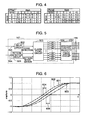
- FIG. 2 shows an example of the recording strategy.
- 201 indicates a record signal to be recorded on an optical disk and 202 is a recording strategy thereof.
- the recording strategy is controlled by laser power (to be referred to as recording power hereinbelow) and a laser pulse edge position (to be referred to as pulse timing hereinbelow).
- the recording power corresponds to Pw, Ps, and Pc in the diagram and the pulse timing corresponds to numerals 206 to 210 in the diagram.
- the diagram shows part of the pulse timing.
- FIG. 3 shows an example of a compensation table to be used for the phase compensation of pulse trains 206 (dTtop) and 208 (Teclp) of FIG. 2 .
- dTtop there are determined pulse timing setting values when the preceding space and the pertinent mark range respectively from 2T to 5T.
- Teclp there are determined pulse timing setting values when the pertinent mark and the succeeding space are respectively from 2T to 5T.
- FIG. 1 shows a system configuration of the first embodiment.
- Information data outputted from a higher-level host 123 via a signal bus 125 is modulated by a modulator circuit 120 into a disk record signal.
- a recording strategy generator circuit 121 generates the recording strategy described above by use of a disk record signal, a pulse timing setting value 155 outputted from a phase shift detector circuit, recording power setting from a microcomputer 124, and the like.
- a laser driver 122 drives a laser 108 according to the recording strategy. Laser light radiated from the laser 108 records via a collimation lens 105 and an objective 103 a mark on an optical disk 101. As a result, data is recorded on the optical disk 101.
- reflected light obtained by radiating laser light onto the optical disk 101 is collected via a beam splitter 104 by a condenser 106 onto a photoelectric conversion element 107 to be converted into an electric signal (to be referred to as a reproduced signal hereinbelow) through processing such as amplification and voltage conversion by an amplifier 109.
- the reproduced signal is inputted via a transmission path such as a flexible cable to a PRML processing circuit.
- the PRML circuit includes an adaptive equalizer circuit 116 and an ML decoder circuit, i.e., a viterbi decoder circuit 117 as its general example.
- the adaptive equalizer circuit 116 equalizes the reproduced signal to a target equalization characteristic and then the viterbi decoder circuit 117 executes binarization processing for the signal according to the equalization characteristic.
- the adaptive equalizer circuit includes an FIR filter 111, an equalization error calculation circuit 112, a filter coefficient calculation circuit 113, a coefficient symmetrization circuit 114, and a switch 115.
- FIG. 3 shows a detailed configuration of the FIR filter 111 of FIG. 1 and its peripheral circuits.
- the FIR filter of this embodiment is a 7-tap filter.
- 301 to 307 indicate delay elements of one-period (1T) units of a reproduction clock synchronized with the reproduced signal
- 308 to 314 are multiplier circuits
- 315 is an adder circuit. Signals obtained by passing the reproduced signal 151 through the respective delay elements are multiplied by predetermined coefficients c3 to -cm3. The results are added to each other to obtain an equalized signal 152.
- the equalization error calculation circuit 114 calculates an error between the equalized signal and the target equalization characteristic.
- the target equalization characteristic is represented as multiplication coefficient values of the FIR filter as for the filter described above.
- an PR(1,2,2,1) characteristic in which the multiplication coefficient values of the 4-tap filter are 1, 2, 2, and 1 are employed as the equalization target.
- PR(1,2,2,1) ten output values from quadripartite-time totaling of binary signals are set as reference values. Table 1 shows these reference values.
- the equalization error calculation circuit outputs an equalization error 153 which is a difference between the reference values and the equalization signal 152 at each point of time.
- the reference value at each point of time is selected from a binary signal pattern which corresponds to the equalization signal and which is produced by the viterbi decoder circuit 171.
- the filter coefficient calculation circuit 113 calculates a setting values of the tap coefficients ranging from cm3 to c3 of the FIR filter 111.
- the coefficient values are updated to minimize the equalization error output 153 using the method of least squares, the steepest-descent method, and the like. For example, in the least square averaging method based on the steepest-descent method, each equalization coefficient is updated according to the following expression by use of the equalization error output 153 and each tap output (d3 to dm3) from the FIR filter 111.
- c * t + 1 c * t X ⁇ ⁇ err ⁇ d * t in the above expression, ⁇ is a converging speed coefficient, which is a value to control the coefficient update speed.
- the coefficient symmetrization circuit 114 is a circuit to average coefficients of tap outputs which are symmetric with respect to the tap center of the FIR filter 111, and includes a divider circuit of 1/2 using an adder circuit, a bit shift, and the like.
- the switch 115 is a switch to select, as the coefficient of the FIR filter 111, an output from the filter coefficient calculation circuit 113 or an output from the coefficient symmetrization circuit 114.
- the equalized signal 152 outputted from the adaptive equalizer circuit 116 is inputted to the viterbi decoder circuit 117.
- the viterbi decoder circuit 117 conducts a branch metrics operation for the inputted equalized signal 152 and accumulates the result in a path memory to thereby output a binary signal.
- the branch metrics operation there is calculated an error between the filter output waveform 152 and a target equalization output obtained by equalizing, by use of PR(1,2,2,1) as the equalization target, all binarization patterns of the modulation rules.
- the path memory selects and outputs, as the binary signal of the equalized signal, a signal pattern for which the total value of the results of the operation takes a minimum value.
- the outputted binary signal is decoded by a decoder circuit 118 into a data signal to be sent to the higher-level host 123.
- a phase shift detector circuit 119 detects a phase shift of the reproduced waveform using the equalization error signal 153.
- FIG. 5 shows structure of the phase shift detector circuit 119.
- a circuit 501 detects mark and space patterns to conduct record compensation based on a viterbi decoding result 154.
- 502 is a delay circuit to match the phase of the equalization error signal 153 with that of pattern information obtained by inputting the viterbi decoding result 154 to a pattern detector circuit 501.
- the equalization error signal 153 is classified according to the mark and space patterns obtained by the pattern detector circuit 401.
- a group of Low Pass Filters (LPF) 504 averages the classified equalization errors to suppress defects and fingerprints on the disk and other local influence in the reproduction.
- LPF Low Pass Filters
- a strategy control quantity calculation circuit 505 compares the equalization errors averaged by the respective mark and space patterns with predetermined target error amounts respectively set in advance, and then conducts, based on the differences therebetween, parameter control of pulse timing associated with the respective mark and space patterns.
- the pulse timing value 155 calculated as above is inputted to the recording strategy generator circuit 121.
- FIG. 6 shows an example of the reproduced waveform.
- the abscissa represents time and the ordinate represents the waveform amplitude.
- 601 indicates an ideal input waveform without any phase shift
- 602 is a waveform phase-shifted forward in the time axis
- 603 is a waveform phase-shifted backward in the time axis.
- the forward phase shift is indicated by 604
- the backward phase shift is indicated by 605. It can be seen from this example that the backward phase shift is larger.
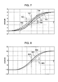
- FIG. 7 shows an equalization output waveform when the waveform of FIG. 6 is passed through a 4-tap fixed characteristic filter having a characteristic of PR(1.2.2.1).
- the abscissa represents time and the ordinate represents amplitude of the waveform.
- the equalization output waveform 601 corresponds to 701
- the equalization output waveform 602 corresponds to 702
- the equalization output waveform 603 corresponds to 703.
- 704 indicates an equalization output waveform when the binary signal of 601 is inputted to the above filter. This is a target equalization output to obtain the equalization error.
- the equalization error at a reproduced waveform edge point 707 is zero in the waveform 701, 705 in the waveform 702, and 706 in the waveform 703. It can be seen that the equalization errors 705 and 706 correspond to the phase shifts 604 and 605, and the polarity and the order in magnitude are kept retained. Hence, in a fixed characteristic filter, by controlling pulse timing of the recording strategy to minimize the equalization error at the edge point of the equalization output of the reproduced waveform, an optimal recording characteristic can be obtained.
- FIG. 8 is a diagram showing an example of a waveform when the adaptive equalization processing is executed for the phase forward-shift waveform 602.
- the abscissa and the ordinate are similar to those of FIGS. 6 and 7 .
- the filter coefficient is controlled to minimize the equalization error.
- the filter coefficient may possibly be controlled, for example, such that the phase shift is set to zero at the edge point 804 as in 801 of the diagram.
- FIG. 9 shows an amplitude characteristic and a group delay characteristic of the filter in this situation.
- the abscissa represents a ratio of the frequency to the reproduction clock
- the ordinate on the left represents the amplitude characteristic
- the ordinate on the right represents the group delay characteristic.
- 901 indicates the amplitude characteristic
- 902 indicates the group delay characteristic of the filter characteristics.
- the group delay characteristic is not fixed.
- a changeover operation is conducted by the switch 115 shown in FIGS. 1 and 3 to select, as the filter coefficient, an output from the coefficient symmetrization circuit 114.
- 903 and 904 of FIG. 9 indicate the amplitude characteristic and the group delay characteristic of the filter when the processing is executed.
- the group delay can be fixed.
- FIG. 10 shows equalized output waveforms when the phase forward-shift waveform 602 and the waveform 601 not including the phase shift are inputted to the filter for which the group delay is fixed.
- the abscissa and the ordinate are similar to those of FIG. 8 .
- 1001 indicates the equalized output waveform of the phase forward-shift waveform 602
- 1002 indicates the equalized output waveform of the waveform 601 not including the phase shift. It is seen that while an equalization error 1003 is detected at an edge point 1004 in the waveform 1001, the error is zero in the waveform 1002.
- FIG. 11 shows a processing sequence in a case wherein the above processing is applied to the recording learning operation, particularly, the pulse timing learning.
- the switch 115 is set not to select the coefficient symmetrization circuit.
- the switch 115 of FIGS. 1 and 3 selects, as the filter coefficients, outputs from the coefficient symmetrization circuit (1102).
- processing such as initialization of the filter coefficients c3 to cm3 may be executed according to necessity.
- data for the recording learning is recorded on a disk (1103). This may be an ordinary data pattern or a special data pattern for the recording learning.
- the recorded data is reproduced and an equalization error is detected by the equalization error calculation circuit 112 (1004) to be classified for each edge pattern by the phase shift detector circuit 119 to calculate the total (1105).
- the equalization error total value of each edge pattern is compared with each predetermined target value, i.e., a predetermined target value beforehand set. If equalization error total value is equal to or less than the predetermined target value for all edge patterns (1106), the switch 115 is changed over to set the filter coefficient symmetrization processing off (1107) and then the learning is terminated (1108). In the operation, as in the processing 1102, processing such as initialization of the filter coefficients c3 to cm3 may be executed according to necessity. If the equalization error total value is more than the predetermined target value for any one edge pattern, the pulse timing is changed for the edge pattern according to the detected equalization error total value (1109), and the data recording is again conducted to adjust the strategy.
- the reproduced waveform edge shift information can be correctly obtained by use of the PRML processing.
- the use of the changeover switch enables both of the securing of the reproduction performance using the PRML processing in the high-speed signal processing on an optical disk and the obtaining of the reproduced waveform edge shift information using the PRML processing in association with increase in the speed of the high-speed learning.
- the above example is an example in which the number of taps of the adaptive equalization filter is an odd number such as 2n+1 (n is an integer). However, if the number of taps is an even number such as 2n (n is an integer), the taps are classified into n right taps and n left taps as shown in FIG. 12 to average the coefficients at tap positions equally apart from both sides, to thereby attain an advantage similar to the advantage described above.
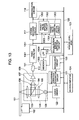
- FIG. 13 shows a system configuration in a second embodiment of the present invention.
- the elements and blocks having the same functions as those of FIG. 1 are assigned with the same reference numerals, and description thereof will be here avoided.
- 1301 indicates an FIR filter for which the coefficient values are fixed.
- the taps of the reproduction clock period and structure to calculate the coefficient values are similar to those of the first embodiment. However, in the present embodiment, since the output from the equalization error detector circuit in the succeeding stage is used to adjust edge timing of the recording strategy, the coefficients of the respective taps are set to fixed values such that the values are symmetric in the time-axis direction.
- FIG. 1303 is a symmetrization circuit to symmetrize the updated target values in a time-axis direction.
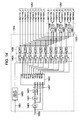
- FIG. 14 shows a detailed circuit diagram of the target value update circuit 1302 and the target value symmetrization circuit 1303. It is assumed that the target values of the viterbi circuit are determined by data for quadripartite-time of binary signals, namely, target values having a restriction length of 4.
- 1401 are delay elements in reproduction channel clock units, the elements convert a binary signal 1352 outputted from the viterbi circuit 117 into a 4-bit parallel signal 1451.
- 1402 is a decoder to convert the 4-bit parallel signal 1451 into eight bits.
- 1403 is a delay circuit to match the phase between the output from the decoder 2 and the output waveform 1351 from the fixed FIR filter 1301.
- a group of switches 1404 include switches which are controlled to be turned on or off according to outputs from the decoder 1402. As a result, there is selected an amplitude value of the filter output waveform 1351 corresponding to each quadripartite-time pattern of the binary signal 1352 to be averaged by a group of LPF 1405 in the succeeding stage.
- adaptive viterbi decoding processing This will be hereinbelow referred to as adaptive viterbi decoding processing and the processing circuit will be referred to as adaptive viterbi decoder circuit.
- the target value 1353 of the adaptive viterbi decoder circuit When the recording learning is conducted by calculating the equalization error as in the first embodiment of the present invention by use of the target value 1353 of the adaptive viterbi decoder circuit and the output 1351 from the fixed FIR filter, the edge phase shift of the reproduced signal is reflected in the target value and the correct equalization error cannot be detected.
- the target value is controlled to fix the group delay characteristic of the target equalization characteristic.
- target values of a pattern symmetric in a time-axis direction are symmetrized by averaging.
- the patterns symmetric in a time-axis direction include the following combinations for the target values with a restriction length of four as indicated in 1303 of FIG. 14 .
- the target values are averaged by adder circuits 1406 and divider circuits 1407 shown in FIG. 14 .
- the equalization characteristic of the rising waveform is equalized to that of the falling waveform, to thereby obtain an advantage similar to the advantage of the coefficient symmetrization when the equalized characteristic is realized by the FIR filter.
- 1304 is a Low Pass Filter (LPF) to average outputs from the equalization error detector circuit and has a function to be reset by the microcomputer 124 according to necessity.
- 1305 indicates a memory capable of storing therein a plurality of combinations each including an equalization error value averaged by the LPF 134 and a recording parameter set to the recording strategy generator circuit.
- LPF Low Pass Filter
- FIG. 15 shows a processing sequence when the above processing is applied to the recording learning operation, particularly to the recording power learning.
- FIG. 2 shows Pw, Ps, Pc, and ratios therebetween.
- the microcomputer 124 of FIG. 13 sets an initial recording power condition to the recording strategy generator circuit 121 and then clears the memory 1305 to be used for the learning (1502).
- the microcomputer 124 records a recording learning data pattern (1503).
- the microcomputer 124 resets and initializes the LPF 1304 (1504).
- the microcomputer 124 reproduces recorded data to detect an equalization error mean value (1505) to store the recording power condition and the equalization error mean value (1506).
- the above processing from 1503 to 1506 is executed for a predetermined number of steps while changing the recording power condition in a predetermined variable step (1507, 1510). After terminating the processing by executing the processing for the predetermined number of steps, the system obtains as shown in FIG.
- a bucket curve 1601 in which the recording power condition and the equalization error mean value stored in the memory by the microcomputer or the like are represented on the abscissa and the ordinate, respectively.
- the system searches for a recording power condition P0 under which the equalization error mean value is minimized in the bucket curve, sets the power as the data recording power to the strategy generator circuit (1508), and terminates the recording power learning (1509). If it is difficult in the processing 1507 to retrieve the minimum value of the equalization error mean value due to the contour of the bucket curve or the like, it may be possible that, for example, an intermediate value P3 of the recording power conditions P1 and P2 for a predetermined equalization error mean value is retrieved as the power condition value.
- the changeover control 1102 and 1107 of the coefficient symmetrization filter is not required. Hence, the processing steps of the recording learning can be accordingly reduced and the recording learning time can be shortened.
- the phase shift can be detected in the stable reproduced waveform by use of the PRML processing as in embodiment 1.
- the recording waveform can be learned by using the phase shift while improving stability of the binarization processing of the viterbi decoding.
- the recording learning processing sequence of the present embodiment there is used a scheme in which the recording is conducted under a plurality of conditions by changing the recording power condition as a recording parameter and then by reproducing the recorded items to extract a recording power condition under which the equalization error total value is minimized.
- the present scheme is also applicable to the pulse timing learning of the first embodiment. In this case, for each mark pattern and each space pattern, a search is made for pulse timing at which the classified equalization error mean value is minimized.
- the pulse timing condition for which the recording compensation table shown in FIG. 4 is not used can be learned in a method similar to the method of the present embodiment.
- FIG. 17 shows a circuit configuration of the third embodiment of the present invention.
- the elements and blocks having the same functions as those of FIGS. 1 and 13 are assigned with the same reference numerals, and description thereof will be here avoided.
- the circuit configuration includes both of the function of the adaptive equalization circuit of the first embodiment and that of the adaptive viterbi decoder circuit of the second embodiment.
- FIG. 18 shows details of a switch 1701.
- the switch 1701 conducts, for the equalization target value to calculate the equalization error in the equalization error detector circuit, a changeover operation between an update target value 1353 generated from the equalized output 152 and the binary signal 1352 and a symmetrization target value 1354 obtained by symmetrizing the symmetrization target value 1353.
- FIG. 18 shows the switch 1701 in detail. In the switch changeover, the update target value 1353 is selected in the ordinary data reproduction.
- the symmetrization target value 1354 is selected.
- 1702 indicates a Low Pass Filter (LPF) to average the equalization error values detected by 112 and has a function to be reset by the microcomputer 124 according to necessity.
- 1703 is a circuit which compares the equalization error mean value attained from 1702 with a predetermined equalization error target value to carry out the recording quality judgment.
- LPF Low Pass Filter
- FIG. 19 shows a processing sequence when the above circuit configuration is applied to the data recording operation associated with the verifying operation.
- the switches 115 and 1751 are set not to select the coefficient symmetrization circuit and the target value symmetrization circuit.
- the recording processing is started (1901)
- the switches 115 and 1751 are set to on to select the filter coefficient symmetrization and the target value symmetrization (1902).
- the microcomputer 124 sets a recording parameter to the recording strategy generator circuit 121 (1903) to record data (1904).
- the microcomputer 124 then resets and initializes an equalization error averaging LPF 1702 (1905) and reproduces the recorded data to detect an equalization error mean value (1906).
- a recording quality judge circuit 1703 compares the equalization error mean value with a predetermined equalization error target value to judge whether or not the equalization error mean value is equal to or less than the predetermined equalization error target value (1907). If the equalization error mean value is equal to or less than the equalization error target value, the switches 115 and 1751 are set to off not to select the filter coefficient symmetrization and the target value symmetrization (1908) and then the recording processing is terminated (1909).
- the equalization error mean value is equal to or more than the equalization error target value in processing 1907, recording failure is assumed and then the recording is conducted again in the same area (1910).
- the recording condition such as the recording parameter may be changed when the recording is conducted again (1911).
- the recording parameter may be changed on the basis of the equalization error mean value or an index value other than the equalization error mean value, for example, a ⁇ value indicating magnitude of the asymmetry of the reproduced waveform.
- the recording quality confirmation is conducted, i.e., data recording including so-called verifying processing is carried out at a high speed
- the recording quality can be correctly judged by use of the adaptive equalization processing. This enables to secure compatibility between the quality evaluation in low-speed recording in which the transmission path band can be fully secured for the signal band and the quality evaluation in high-speed recording in which it is difficult to secure the transmission path band.
- FIG. 20 shows a circuit configuration of the fourth embodiment of the present invention.
- the elements and blocks having the same functions as those of FIGS. 1 and 17 are assigned with the same reference numerals, and description thereof will be here avoided.
- a lens tilt control circuit 2002 controls an actuator 2001 to change magnitude of the tilt of the objective 103 with respect to the disk 101.
- the control circuit 2002 stores in a memory 2003 a pair of the control quantity of the actuator 2001 for each of a plurality of conditions and the equalization error mean value outputted from the LPF 1702, and makes a search for an optimal value of the magnitude of tilt for the objective.
- FIG. 21 shows a flow of the processing.
- the switch 115 is set not to select the coefficient symmetrization circuit.
- the switch 115 of FIG. 20 selects, as the filter coefficient, the output from the coefficient symmetrization processing circuit (2102). In this situation, there may be executed processing such as initialization of the filter coefficient according to necessity.
- the microcomputer 124 sets an initial lens tilt condition and clears the memory 2003 to be used for the learning (2103). The microcomputer 124 then resets and initializes the LPF 1702 (2104) and reproduces data in a predetermined area (2105).
- the microcomputer 124 stores in the memory 2003 a pair of the lens tilt setting condition and the obtained adaptive equalization mean value (2106).
- the processing from 2104 to 2106 is executed for a predetermined number of steps while changing the lens tilt condition by a predetermined variable step (2107, 2110).
- the system obtains as shown in FIG. 22 a bucket curve 2201 in which the lens shift condition and the equalization error mean value stored in the memory by the microcomputer or the like are represented on the abscissa and the ordinate, respectively.
- the system selects, as the lens shift setting for the data reproduction, a lens shift condition L0 under which the equalization error mean value is minimized in the bucket curve (2108), and terminates the lens shift learning (2109). If it is difficult in the processing 2108 to retrieve the minimum value of the equalization error mean value due to the contour of the bucket curve or the like, it is possible that, for example, an intermediate value L3 of the lens shift conditions L1 and L2 for predetermined equalization error mean value 2202 is used as the lens shift condition value as the search result.
- the lens tilt condition is employed as the parameter to be learned in the present embodiment.
- the servo condition in the recording and the reproduction for example, the offset value and the loop gain value in the focusing and tracking, it is possible to obtain the optimal value by use of a scheme similar to that of the present embodiment.
- the optimal values can be obtained by using a scheme similar to the above scheme.
- the embodiments there are shown adaptation by a 7-tap FIR filter, a fixed equalization circuit, and an example of a restricted length of four in which the PR(1,2,2,1) characteristic is set as the equalization target characteristic for the PR class.
- a viterbi decoder circuit is employed as a binarization processing circuit conducting the ML decoding.
- the number of taps of the FIR filter and the restriction length and the PR class in the equalization target characteristic are not related to the gist of the present invention, and hence are not restricted by the embodiments.
- the binarization processing circuit is not restricted by the viterbi decoder circuit.
- symmetrization of the tap coefficients of the FIR filter has been described as a scheme to fix the group delay characteristic of the equalization characteristic of the adaptive equalization circuit.
- the circuit to implement the adaptive equalization processing may also be configured in other ways. In this case, it is only necessary to add, in addition to the adaptive equalization processing, control processing to fix the group delay characteristic of the filter circuit.
- the method of detecting the group delay in this situation may be implemented such that for example, for a signal of which the characteristic is known, control is carried out to equalize the equalization error in the rising pattern and the falling pattern.
- the mean value of equalization errors at the reproduced waveform edge point is employed as an item to evaluate the optimal value and to confirm the recording quality in the pulse timing learning and the recording power learning.
- the present invention is always applicable to a case wherein the equalized output waveform in the PRML processing is used for the processing described above.
- the indices of the optimal value evaluation and the recording quality confirmation are not restricted by the contents described in conjunction with the embodiments.
- the present invention enables both of the securing of quality in the information reproduction through the PRML processing from a recording medium and the evaluation of reproduced signals by use of ML decoder such as the PRML processing in the high-speed recording and reproduction.
- the recording parameter and the servo parameter can be stably adjusted through the stable information reproduction and the detection of the signal edge phase shift by use of the PRML. That is, the high-speed recording and reproduction by realizing a high transfer rate for the to-be-recorded information and reproduced information and various adjustments can be conducted at one and the same speed.
- Heat generated due to increase in the motor load caused by the speed change can be reduced and occurrence of the rotary regulation wait time associated with the speed change can be suppressed. It is hence possible to implement the stabilization and power saving in the recording learning operation as well as to minimize the learning time.
Landscapes
- Engineering & Computer Science (AREA)
- Signal Processing (AREA)
- Physics & Mathematics (AREA)
- Optics & Photonics (AREA)
- Optical Recording Or Reproduction (AREA)
- Signal Processing For Digital Recording And Reproducing (AREA)
Applications Claiming Priority (1)
| Application Number | Priority Date | Filing Date | Title |
|---|---|---|---|
| JP2008158624A JP5081737B2 (ja) | 2008-06-18 | 2008-06-18 | 光学的情報記録方法、光学的情報再生方法、および光ディスク装置 |
Publications (2)
| Publication Number | Publication Date |
|---|---|
| EP2136369A2 true EP2136369A2 (de) | 2009-12-23 |
| EP2136369A3 EP2136369A3 (de) | 2010-02-17 |
Family
ID=41016837
Family Applications (1)
| Application Number | Title | Priority Date | Filing Date |
|---|---|---|---|
| EP09251573A Withdrawn EP2136369A3 (de) | 2008-06-18 | 2009-06-16 | Optisches Informationsaufzeichnungsverfahren, optisches Informationswiedergabeverfahren und optisches Plattengerät |
Country Status (4)
| Country | Link |
|---|---|
| US (2) | US8208358B2 (de) |
| EP (1) | EP2136369A3 (de) |
| JP (1) | JP5081737B2 (de) |
| CN (2) | CN101609695B (de) |
Families Citing this family (19)
| Publication number | Priority date | Publication date | Assignee | Title |
|---|---|---|---|---|
| JP2011103153A (ja) * | 2009-11-10 | 2011-05-26 | Renesas Electronics Corp | 情報検出装置及び光ディスク装置 |
| JP2013062000A (ja) * | 2010-01-18 | 2013-04-04 | Panasonic Corp | 光ディスク記録再生装置 |
| JP4812881B2 (ja) | 2010-01-20 | 2011-11-09 | 日立コンシューマエレクトロニクス株式会社 | 記録条件の調整方法及び光ディスク装置 |
| JP5553655B2 (ja) * | 2010-03-26 | 2014-07-16 | 株式会社日立エルジーデータストレージ | 光ディスクの記録品質評価方法及び光ディスクストレージ装置 |
| JP4988901B2 (ja) * | 2010-06-21 | 2012-08-01 | 日立コンシューマエレクトロニクス株式会社 | 記録条件の調整方法、光ディスク装置及び情報記録方法 |
| JP5507482B2 (ja) * | 2011-02-23 | 2014-05-28 | 日立コンシューマエレクトロニクス株式会社 | 再生信号評価方法、情報記録再生方法、及び情報記録再生装置 |
| JP2012185875A (ja) * | 2011-03-04 | 2012-09-27 | Renesas Electronics Corp | 半導体装置、記録ストラテジー生成方法、及び記録ストラテジー生成用プログラム |
| US8983218B2 (en) | 2012-04-11 | 2015-03-17 | Texas Instruments Incorporated | Virtual boundary processing simplification for adaptive loop filtering (ALF) in video coding |
| JP5373164B2 (ja) * | 2012-08-31 | 2013-12-18 | 日立コンシューマエレクトロニクス株式会社 | 光学的情報記録方法、光学的情報再生方法、および光ディスク装置 |
| US10134438B2 (en) | 2013-06-28 | 2018-11-20 | Sony Corporation | Optical medium reproduction apparatus and method of reproducing optical medium |
| US9843389B2 (en) | 2013-08-14 | 2017-12-12 | Sony Corporation | Optical medium reproduction device and optical medium reproduction method |
| JP6167918B2 (ja) * | 2013-08-14 | 2017-07-26 | ソニー株式会社 | 光媒体再生装置および光媒体再生方法 |
| JPWO2015107572A1 (ja) * | 2014-01-17 | 2017-03-23 | パナソニックIpマネジメント株式会社 | 情報記録再生装置、及び情報記録再生方法 |
| EP3252772B1 (de) * | 2015-01-30 | 2019-08-21 | Sony Corporation | Wiedergabevorrichtung und wiedergabeverfahren |
| US10667690B2 (en) * | 2016-04-02 | 2020-06-02 | Intel Corporation | Compressive sensing sparse sampling photoplethysmogram (PPG) measurement |
| CN113286306A (zh) * | 2021-05-26 | 2021-08-20 | 中国人民解放军火箭军工程大学 | 一种基于信道均衡的无线信道指纹滤除方法及系统 |
| CN115704875B (zh) * | 2021-08-16 | 2026-04-14 | 浙江正泰电器股份有限公司 | 互感器接线检测方法、万能式断路器及设备 |
| CN114495895B (zh) * | 2021-12-22 | 2025-11-07 | 北京百度网讯科技有限公司 | 对称音频的获取方法、装置、电子设备及存储介质 |
| CN121037462B (zh) * | 2025-10-28 | 2026-01-30 | 国网吉林省电力有限公司洮南市供电公司 | 面向电网故障定位的高精度录波采集与时标同步系统 |
Citations (3)
| Publication number | Priority date | Publication date | Assignee | Title |
|---|---|---|---|---|
| JP2004178627A (ja) | 2002-11-25 | 2004-06-24 | Hitachi Ltd | ビタビ復号回路および情報再生装置 |
| WO2005031743A1 (ja) | 2003-09-30 | 2005-04-07 | Matsushita Electric Industrial Co., Ltd. | 評価装置および評価方法 |
| JP2005339690A (ja) | 2004-05-27 | 2005-12-08 | Nec Corp | 情報記録媒体への記録方法及び情報記録再生装置並びに情報記録媒体 |
Family Cites Families (22)
| Publication number | Priority date | Publication date | Assignee | Title |
|---|---|---|---|---|
| JP3351163B2 (ja) | 1994-07-27 | 2002-11-25 | 株式会社日立製作所 | 情報記録再生装置及び信号処理回路 |
| JP3716175B2 (ja) | 1994-07-27 | 2005-11-16 | 株式会社日立グローバルストレージテクノロジーズ | 信号処理回路及び情報記録再生装置 |
| US6654325B1 (en) | 1999-08-09 | 2003-11-25 | Hitachi, Ltd. | Trial writing method and optical disk system using the same |
| JP2001155429A (ja) | 1999-11-25 | 2001-06-08 | Hitachi Ltd | 自動等化回路及びそれを用いた再生装置 |
| JP3486145B2 (ja) * | 2000-01-17 | 2004-01-13 | 松下電器産業株式会社 | デジタル記録データ再生装置 |
| JP4072751B2 (ja) * | 2001-04-20 | 2008-04-09 | 日本ビクター株式会社 | 再生装置 |
| CN1306516C (zh) * | 2001-11-09 | 2007-03-21 | 株式会社东芝 | 信息记录/还原系统和记录校正方法 |
| EP1553566B1 (de) * | 2002-07-01 | 2010-05-19 | Panasonic Corporation | Optischer datenträger, aufzeichnungseinrichtung mit optischem datenträger, aufzeichnungsverfahren mit optischem datenträger |
| JP3749889B2 (ja) * | 2002-10-17 | 2006-03-01 | 株式会社東芝 | Prml検出を適用する信号処理デバイス、同デバイスを備えたディスク記憶装置、及び同装置におけるフィードバック制御のための信号処理方法 |
| JP2004178267A (ja) | 2002-11-27 | 2004-06-24 | Sony Corp | メモリ回路生成方法および装置、メモリ回路、回路モデル検証方法および装置、回路モデル生成方法および装置 |
| JP2005135561A (ja) * | 2003-10-31 | 2005-05-26 | Sanyo Electric Co Ltd | データ再生装置 |
| US7646686B2 (en) * | 2003-11-06 | 2010-01-12 | Panasonic Corporation | Recording/reproduction apparatus which adjusts recording power based on a partial response maximum likelihood (PRML) technique |
| WO2005045829A1 (ja) * | 2003-11-11 | 2005-05-19 | Matsushita Electric Industrial Co., Ltd. | フィルタ係数調整回路 |
| US7477584B2 (en) | 2003-11-11 | 2009-01-13 | Samsung Electronics Co., Ltd. | Recording and/or reproducing apparatus and method with a signal quality determining device and method |
| JP4377677B2 (ja) * | 2003-12-25 | 2009-12-02 | 株式会社東芝 | ディスク装置及びディスク再生方法 |
| KR100528878B1 (ko) * | 2004-02-16 | 2005-11-16 | 삼성전자주식회사 | 데이터 저장을 위한 고속 혼성 아날로그/디지털 prml데이터 검출 및 클럭 복원 장치 |
| JP4313755B2 (ja) * | 2004-05-07 | 2009-08-12 | 株式会社日立製作所 | 再生信号の評価方法および光ディスク装置 |
| JP2006127679A (ja) * | 2004-10-29 | 2006-05-18 | Toshiba Corp | 光ディスク装置及び光ディスク再生方法 |
| JPWO2007010993A1 (ja) * | 2005-07-20 | 2009-01-29 | パナソニック株式会社 | 波形等化制御装置 |
| JP2007149180A (ja) | 2005-11-25 | 2007-06-14 | Hitachi Ltd | 光ディスク装置 |
| JP4826438B2 (ja) * | 2006-11-15 | 2011-11-30 | 株式会社日立製作所 | 光ディスク記録装置、および、光ディスク記録方法。 |
| JP5019951B2 (ja) * | 2007-05-29 | 2012-09-05 | 三菱電機株式会社 | 光記録方法及び光記録装置 |
-
2008
- 2008-06-18 JP JP2008158624A patent/JP5081737B2/ja not_active Expired - Fee Related
-
2009
- 2009-05-18 CN CN200910141609XA patent/CN101609695B/zh not_active Expired - Fee Related
- 2009-05-18 CN CN2013102594103A patent/CN103354094A/zh active Pending
- 2009-06-16 EP EP09251573A patent/EP2136369A3/de not_active Withdrawn
- 2009-06-16 US US12/485,131 patent/US8208358B2/en not_active Expired - Fee Related
-
2012
- 2012-05-24 US US13/479,734 patent/US8649248B2/en not_active Expired - Fee Related
Patent Citations (3)
| Publication number | Priority date | Publication date | Assignee | Title |
|---|---|---|---|---|
| JP2004178627A (ja) | 2002-11-25 | 2004-06-24 | Hitachi Ltd | ビタビ復号回路および情報再生装置 |
| WO2005031743A1 (ja) | 2003-09-30 | 2005-04-07 | Matsushita Electric Industrial Co., Ltd. | 評価装置および評価方法 |
| JP2005339690A (ja) | 2004-05-27 | 2005-12-08 | Nec Corp | 情報記録媒体への記録方法及び情報記録再生装置並びに情報記録媒体 |
Also Published As
| Publication number | Publication date |
|---|---|
| JP2010003328A (ja) | 2010-01-07 |
| EP2136369A3 (de) | 2010-02-17 |
| US20120243393A1 (en) | 2012-09-27 |
| CN101609695B (zh) | 2013-07-31 |
| JP5081737B2 (ja) | 2012-11-28 |
| US20090316561A1 (en) | 2009-12-24 |
| US8649248B2 (en) | 2014-02-11 |
| CN101609695A (zh) | 2009-12-23 |
| CN103354094A (zh) | 2013-10-16 |
| US8208358B2 (en) | 2012-06-26 |
Similar Documents
| Publication | Publication Date | Title |
|---|---|---|
| US8208358B2 (en) | Optical information recording method, optical information reproduction method and optical disk device | |
| KR100490498B1 (ko) | 디지털 기록 데이터 재생 장치 | |
| US7551668B2 (en) | Adaptive equalizing apparatus and method | |
| KR101049695B1 (ko) | 기록 제어 장치, 기록 및 재생 장치, 및 기록 제어 방법 | |
| US8165007B2 (en) | Information detection device and optical disc device | |
| US20040114912A1 (en) | Reproduction signal processing device | |
| US8284648B2 (en) | Optical disk recording apparatus | |
| EP1467367A2 (de) | Methode zur Entzerrung reproduzierter Signale von optischen Informationsmedien und Wiedergabe-/Aufnahmegerät optischer Information | |
| US8787135B2 (en) | Signal processing device, signal processing method, and optical disc apparatus | |
| US6992964B2 (en) | Information reproducing device and information reproducing method | |
| US9117485B2 (en) | Signal processing apparatus capable of suppressing non-linear noise component during reading optical recording medium | |
| US7839735B2 (en) | Phase difference detection apparatus, phase difference detection method, reproduction apparatus and tracking controlling method | |
| JP5373164B2 (ja) | 光学的情報記録方法、光学的情報再生方法、および光ディスク装置 | |
| US20070041300A1 (en) | Optical disk apparatus and reproduction signal processing circuit | |
| JP2007059018A (ja) | 情報信号再生装置、方法、及び、光ディスク再生装置 | |
| WO2007072346A1 (en) | Leakage scheme for a receiver. | |
| JP2005259317A (ja) | 多値情報再生方法,多値情報記録媒体,多値情報波形等化装置,多値情報再生装置,多値情報記録装置 | |
| JP2000156041A (ja) | 光情報再生装置および光情報再生方法 | |
| US20090316557A1 (en) | Information reproducing apparatus and method, and computer program | |
| JP2011253604A (ja) | 光学的情報記録再生装置 | |
| US20080298199A1 (en) | Writing strategy parameters indexing method and recording apparatus therefor | |
| JP2000348361A (ja) | 光ディスク装置 | |
| JP2002319231A (ja) | 光学的情報記録再生装置 |
Legal Events
| Date | Code | Title | Description |
|---|---|---|---|
| PUAI | Public reference made under article 153(3) epc to a published international application that has entered the european phase |
Free format text: ORIGINAL CODE: 0009012 |
|
| 17P | Request for examination filed |
Effective date: 20090702 |
|
| AK | Designated contracting states |
Kind code of ref document: A2 Designated state(s): AT BE BG CH CY CZ DE DK EE ES FI FR GB GR HR HU IE IS IT LI LT LU LV MC MK MT NL NO PL PT RO SE SI SK TR |
|
| PUAL | Search report despatched |
Free format text: ORIGINAL CODE: 0009013 |
|
| AK | Designated contracting states |
Kind code of ref document: A3 Designated state(s): AT BE BG CH CY CZ DE DK EE ES FI FR GB GR HR HU IE IS IT LI LT LU LV MC MK MT NL NO PL PT RO SE SI SK TR |
|
| AX | Request for extension of the european patent |
Extension state: AL BA RS |
|
| RAP1 | Party data changed (applicant data changed or rights of an application transferred) |
Owner name: HITACHI CONSUMER ELECTRONICS CO., LTD. |
|
| 17Q | First examination report despatched |
Effective date: 20130805 |
|
| STAA | Information on the status of an ep patent application or granted ep patent |
Free format text: STATUS: THE APPLICATION IS DEEMED TO BE WITHDRAWN |
|
| 18D | Application deemed to be withdrawn |
Effective date: 20180103 |