EP2124130A2 - Paketprozessor, Paketsteuerungsverfahren und Paketsteuerungsprogramm - Google Patents
Paketprozessor, Paketsteuerungsverfahren und Paketsteuerungsprogramm Download PDFInfo
- Publication number
- EP2124130A2 EP2124130A2 EP20090157907 EP09157907A EP2124130A2 EP 2124130 A2 EP2124130 A2 EP 2124130A2 EP 20090157907 EP20090157907 EP 20090157907 EP 09157907 A EP09157907 A EP 09157907A EP 2124130 A2 EP2124130 A2 EP 2124130A2
- Authority
- EP
- European Patent Office
- Prior art keywords
- packet
- processing unit
- clock frequency
- frequency control
- clock
- Prior art date
- Legal status (The legal status is an assumption and is not a legal conclusion. Google has not performed a legal analysis and makes no representation as to the accuracy of the status listed.)
- Granted
Links
Images


Classifications
-
- G—PHYSICS
- G06—COMPUTING OR CALCULATING; COUNTING
- G06F—ELECTRIC DIGITAL DATA PROCESSING
- G06F1/00—Details not covered by groups G06F3/00 - G06F13/00 and G06F21/00
- G06F1/26—Power supply means, e.g. regulation thereof
- G06F1/32—Means for saving power
- G06F1/3203—Power management, i.e. event-based initiation of a power-saving mode
-
- G—PHYSICS
- G06—COMPUTING OR CALCULATING; COUNTING
- G06F—ELECTRIC DIGITAL DATA PROCESSING
- G06F1/00—Details not covered by groups G06F3/00 - G06F13/00 and G06F21/00
- G06F1/26—Power supply means, e.g. regulation thereof
- G06F1/32—Means for saving power
- G06F1/3203—Power management, i.e. event-based initiation of a power-saving mode
- G06F1/3234—Power saving characterised by the action undertaken
- G06F1/324—Power saving characterised by the action undertaken by lowering clock frequency
-
- Y—GENERAL TAGGING OF NEW TECHNOLOGICAL DEVELOPMENTS; GENERAL TAGGING OF CROSS-SECTIONAL TECHNOLOGIES SPANNING OVER SEVERAL SECTIONS OF THE IPC; TECHNICAL SUBJECTS COVERED BY FORMER USPC CROSS-REFERENCE ART COLLECTIONS [XRACs] AND DIGESTS
- Y02—TECHNOLOGIES OR APPLICATIONS FOR MITIGATION OR ADAPTATION AGAINST CLIMATE CHANGE
- Y02D—CLIMATE CHANGE MITIGATION TECHNOLOGIES IN INFORMATION AND COMMUNICATION TECHNOLOGIES [ICT], I.E. INFORMATION AND COMMUNICATION TECHNOLOGIES AIMING AT THE REDUCTION OF THEIR OWN ENERGY USE
- Y02D10/00—Energy efficient computing, e.g. low power processors, power management or thermal management
Definitions
- This invention relates to a packet processor for performing predetermined processing on an input packet and outputting the processed packet, a packet control method implemented by this packet processor, and a packet control program for implementing the packet control method.
- This invention in particular relates to a packet processor having one or two or more packet processing units and designed to supply a clock of a predetermined frequency to each of the packet processing units, a packet control method implemented by this packet processor, and a packet control program for implementing the packet control method.
- the effort of power reduction is mainly pursued from the viewpoint of device technologies aiming at reduction of the operating voltage accompanied by the increased degree of integration and miniaturization of electronic components.
- This technique aims to reduce the average power consumption by reducing the stationary operating power and the power consumption during the stand-by state.
- special development tools are required for design and verification in order to employ such asynchronous circuit architecture and method for common electronic components such as ASICs (Application Specific Integrated Circuits) and FPGAs (Field Programmable Gate Arrays).
- ASICs Application Specific Integrated Circuits
- FPGAs Field Programmable Gate Arrays
- These types of packet processors have a plurality of packet processing units. Each of these packet processing units is constantly supplied with a clock regardless of whether or not it has a packet to process. Therefore, considerably large power is consumed when no packet is processed.
- a preceding processing unit monitors whether or not there exists data to be processed by a subsequent processing unit.
- the clock supply to the subsequent processing unit is controlled based on a monitoring result. In this manner, the wireless communication device is allowed to reduce the power consumption according to the amount of data to be processed.
- this wireless communication device is only capable of dealing with received signals having a specific frame configuration, and is not capable of processing variable-length packets or responding to variation in processing time in the processing units. Consequently, the technology of this wireless communication device is not applicable directly to packet processors.
- This invention has been made in view of the circumstances described above, and it is an object of the invention to provide a packet processor the input traffic capacity of which varies and which is capable of reducing the power consumption when receiving a low capacity traffic that is lower than the maximum capacity without impairing the throughput obtained when the input traffic capacity is at its maximum, a packet control method implemented by such a packet processor, and a packet control program for implementing the packet control method.
- an aspect of this invention provides a packet processor having one or two or more packet processing units, which is provided with a packet detector (or detecting means) for detecting whether or not a packet exists in the packet processing unit and outputting a packet detection signal indicating a result of the detection; and a clock frequency controller (or controlling means) for controlling a frequency of a clock supplied to the packet processing unit based on the packet detection signal.
- Another aspect of this invention provides a packet control method for performing predetermined processing on an input packet and outputting the processed packet, and the method includes: detecting whether or not a packet exists in a packet processing unit for performing the predetermined processing; and performing a frequency squeezing control on a clock supplied to the packet processing unit when no packet exists in the packet processing unit.
- Still another aspect of this invention provides a packet control program for causing a packet processor to perform predetermined processing on a packet input thereto and to output the processed packet, and the processing includes: detecting whether or not a packet exists in the packet processing unit for performing the predetermined processing; and performing a frequency squeezing control on a clock supplied to the packet processing unit when no packet exists in the packet processing unit.
- Fig. 1 is a functional block diagram illustrating packet processing by a packet processor 100 the input traffic capacity of which varies.
- a packet input terminal 111 receives supply of an input packet.
- a packet input clock input terminal 112 receives supply of a clock (signal).
- a packet buffer F 113 takes in and accumulates the packet supplied to the packet input terminal 111 in synchronization with the clock supplied to the packet input clock input terminal 112.
- the packet buffer F 113 transfers the accumulated packet to a packet processing unit A 114. Once the packet is transferred from the packet buffer F 113 to the packet processing unit A 114, the packet processing unit A 114 performs first packet processing A on the packet.
- the packet processing unit A 114 transfers the packet having undergone the processing A to a packet processing unit B 116.
- the packet processing unit B 116 performs second packet processing B on the packet.
- the packet processing unit B 116 transfers the packet having undergone the processing B to a packet processing unit C 118.
- the packet processing unit C 118 performs third packet processing C on the packet.
- the packet processing unit C 118 transfers the packet having undergone the processing C to a packet buffer G 119.
- the packet buffer G 119 once accumulates the packet received from the packet processing unit C 118, and outputs the packet from a packet output terminal 120 in synchronization with a clock supplied to a packet output clock input terminal 121.
- a clock distributor 123 generates clocks of optimal frequencies for the respective component blocks (frequencies fa, fb and fc, in this example) in response to a clock supplied to a clock input terminal 122, and supplies the generated clocks to the component blocks.
- an input packet is output after having undergone a plurality of processing operations.
- the packet processor and the packet control method according to the exemplary embodiments described below can be realized by a computer implementing the packet control program of the invention.
- the packet control program is provided, for example, by means of a recording medium.
- the recording medium may be, for example, a magnetic disk, an optical disk, a semiconductor memory, or any other computer-readable recording medium.
- the packet control program recorded on a recording medium can be installed into the computer either by directly loading the recording medium into the computer, or via a communication line.
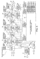
- Fig. 2 is a block diagram showing a configuration of a packet processor 1a according to this embodiment.
- This packet processor 1a is a packet processor capable of dealing with variation in input traffic capacity.
- the packet processor 1a has a packet input terminal 11, a packet input clock input terminal 12, a packet buffer F 13, a packet processing unit A 14, a clock transfer unit D 15, block packet detector (detecting means) A 16, a packet processing unit B 17, clock transfer unit E 18, block packet detector (detecting means) B 19, a packet processing unit C 20, block packet detector (detecting means) C 21, a packet buffer G 22, a packet output clock input terminal 23, a packet output terminal 24, a clock distributor 25, a clock input terminal 26, a clock frequency control unit A 27, a clock frequency control unit B 28, a clock frequency control unit C 29, a setting information input terminal 30, a clock frequency control information setting unit 31, a clock frequency control instruction unit 32.
- the packet input terminal 11 receives supply of an input packet.
- the packet input clock input terminal 12 receives supply of a clock.
- the packet buffer F 13 takes in the packet supplied to the packet input terminal 11 in synchronization with the clock supplied to the packet input clock input terminal 12.
- the packet buffer F (input-side packet buffer) 13 accumulates the packet input through the packet input terminal 11.
- the packet buffer F 13 transfers the accumulated packet to the packet processing unit A 14.
- the packet buffer F 13 transmits a packet non-detection signal F to the clock frequency control instruction unit 32.
- the packet non-detection signal F indicates logic "1" when no packet is accumulated in the packet buffer F 13, whereas indicates logic "0" when a packet is accumulated therein.
- the packet processing unit A 14 performs first packet processing A on the packet.
- the packet processing unit A 14 then transfers the packet having undergone the processing A to the packet processing unit B 17 via the clock transfer unit D 15.
- the block packet detector A 16 monitors packets input to and output from the packet processing unit A 14, and sends a packet non-detection signal A to the clock frequency control instruction unit 32.
- the packet non-detection signal A indicates logic "1" when no packet exists in the packet processing unit A 14, whereas indicates logic "0" when a packet exists therein.
- the packet processing unit B 17 performs second packet processing B on the packet received via the clock transfer unit D 15.
- the packet processing unit B 17 then transfers the packet having undergone the processing B to the packet processing unit C 20 via the clock transfer unit E 18.
- the block packet detector B 19 monitors packets input to and output from the packet processing unit B 1, and sends a packet non-detection signal B to the clock frequency control instruction unit 32.
- the packet non-detection signal B indicates logic "1" when no packet exists in the packet processing unit B 17, whereas indicates logic "0" when a packet exists therein.
- the packet processing unit C 20 performs third packet processing C on the packet received via the clock transfer unit E 18. The packet processing unit C 20 then transfers the packet having undergone the processing C to the packet buffer G 22.
- the block packet detector C 21 monitors packets input to and output from the packet processing unit C 20, and sends a packet non-detection signal C to the clock frequency control instruction unit 32.
- the packet non-detection signal C indicates logic "1" when no packet exists in the packet processing unit C 20, whereas indicates logic "0" when a packet exists therein.
- the packet buffer G (output-side packet buffer) 22 outputs the packet from the packet output terminal 24 in synchronization with a clock supplied to the packet output clock input terminal 23.
- the block packet detector A 16, the block packet detector B 19, and the block packet detector C 21 monitor the numbers of packets input to and output from the packet processing unit A 14, the packet processing unit B 17, and the packet processing unit C 20, respectively.
- the relevant block packet detector A, B, or C determines that there is no packet accumulated in the corresponding packet processing unit A, B, or C.
- This function can be performed by an add-subtract counter which adds one each time a packet is input and subtracts one each time a packet is output.
- the clock transfer unit D 15 and the clock transfer unit E 18 are well-known to those skilled in the art, and are not directly related to this invention. Therefore, detailed description of these clock transfer units will be omitted.
- a technology relating to a clock transfer unit is disclosed, for example, in Japanese Laid-Open Patent Publication No. H06-69913 .
- the clock distributor 25 generates clocks (or clock signals) of optimal frequencies for the respective component blocks based on a clock supplied from a clock input terminal 122, and distributes the generated clocks to the component blocks.
- clocks to be distributed have three different frequencies fa, fb, and fc.
- clocks having different frequencies may be distributed to different component blocks, respectively.
- clocks having the same frequency may be distributed in common to two or more component blocks.
- the clock frequency control unit A 27 Based on a clock frequency control signal A received from the clock frequency control instruction unit 32, the clock frequency control unit A 27 sends the clock distributed by the clock distributor 25 to the packet processing unit A 14 after (or without) squeezing the clock frequency fa (reducing the frequency with the minimum value set to zero).
- the clock frequency control unit B 28 Based on a clock frequency control signal B received from the clock frequency control instruction unit 32, the clock frequency control unit B 28 sends the clock distributed by the clock distributor 25 to the packet processing unit B 17 after (or without) squeezing the clock frequency fb (reducing the frequency with the minimum value set to zero).
- the clock frequency control unit C 29 Based on a clock frequency control signal C received from the clock frequency control instruction unit 32, the clock frequency control unit C 29 sends the clock distributed by the clock distributor 25 to the packet processing unit C 20 after (or without) squeezing the clock frequency fc (reducing the frequency with the minimum value set to zero).
- the clock frequency control units 27, 28, and 29 are thus designed such that they can squeeze (reduce) the frequencies of the clock distributed to the packet processing units 14, 17, and 20.
- the setting information input terminal 30 receives information relating to the frequency squeezing, for example, information on squeezed frequencies or squeezing ratio of one n-th of the original clock frequencies fa, fb, and fc.
- the clock frequency control information setting unit 31 sends the information input to the setting information input terminal 30 to the clock frequency control unit A 27, the clock frequency control unit B 28, and the clock frequency control unit C 29.
- the clock frequency control unit A 27, the clock frequency control unit B 28, and the clock frequency control unit C 29 each determine a squeeze frequency when instructed to squeeze by the clock frequency control signals A, B, and C.
- the clock frequency to squeeze is set for example to one n-th instead of being set to zero. This is an example of measures for avoiding the risk of a failure that may occur in the circuit operation of the component block receiving the supply of a clock the frequency of which is reduced to zero.
- this example of setting the squeezing ratio to one n-th has an effect to prevent the increase of power consumption by reducing the scale of the circuit for squeezing the frequency in each of the clock frequency control units.
- the frequency squeezing may be repeated at predetermined intervals while stepwise increasing the value of n, like one half, one fourth, and one eighth.
- the clock frequency control information setting unit 31 may be set by a program having processor functions not shown in Fig. 2 .
- the clock frequency control instruction unit 32 receives a packet non-detection signal F from the packet buffer F 13, a packet non-detection signal A from the block packet detector A 16, a packet non-detection signal B from the block packet detector B 19, and a packet non-detection signal C from the block packet detector C 21, and generates a clock frequency control signal A, a clock frequency control signal B, and a clock frequency control signal C with reference to a clock frequency control logic table shown in Fig. 3 .
- the clock frequency control instruction unit 32 then sends the clock frequency control signals A, B, and C thus generated to the clock frequency control unit A 27, the clock frequency control unit B 28, and the clock frequency control unit C 29, respectively.
- the packet processing unit A 14, the packet processing unit B 17, and the packet processing unit C 20 are instructed whether or not the frequencies fa, fb, and fc of the clocks distributed thereto are to be squeezed.
- the clock frequency control unit A 27, the clock frequency control unit B 28, the clock frequency control unit C 29, and the clock frequency control instruction unit 32 are collectively referred to as the "clock frequency controller (clock frequency squeezing controller)". They are also referred to as the clock frequency controlling means.
- the packet processor according to this embodiment is capable of reducing the operating power consumption of the packet processing units by squeezing the clock frequency (reducing the clock frequency with the minimal value set to zero) supplied to a packet processing unit when there exists no packet in that packet processing unit (and in the preceding packet processing unit). This provides an effect of reduction of the average power consumption.
- this embodiment provides an effect of reducing the average power consumption by reducing the clock frequency although the reduction is not so marked as when the clock frequency is made zero.
- the packet buffer F 13 receives a packet from the packet input terminal 11 in synchronization with a clock input to the packet input clock input terminal 12, and accumulates the received packet.
- the packet buffer F 13 sends to the clock frequency control instruction unit 32 a packet non-detection signal F indicating logic "1" when no packet is accumulated in the packet buffer F 13. In contrast, the packet buffer F 13 sends to the clock frequency control instruction unit 32 a packet non-detection signal F indicating logic "0" when a packet is accumulated therein.
- the packet buffer F 13 transfers a packet to the packet processing unit A 14.
- the packet processing unit A 14 performs first packet processing A on the packet.
- the block packet detector A 16 monitors packets input to and output from the packet processing unit A 14, and sends a packet non-detection signal A indicating logic "1" to the clock frequency control instruction unit 32 when no packet exists in the packet processing unit A 14. In contrast, when a packet exists in the packet processing unit A 14, the block packet detector A 16 sends a packet non-detection signal A indicating logic "0" to the clock frequency control instruction unit 32.
- the packet processing unit A 14 transfers the packet having undergone the processing A to the packet processing unit B 17 via the clock transfer unit D 15.
- the packet processing unit B 17 performs second packet processing B on the packet.
- the block packet detector B 19 monitors packets input to and output from the packet processing unit B 17, and sends a packet non-detection signal B indicating logic "1" to the clock frequency control instruction unit 32 when no packet exists in the packet processing unit B 17. In contrast, when a packet exists in the packet processing unit B 17, the block packet detector B 19 sends a packet non-detection signal B indicating logic "0" to the clock frequency control instruction unit 32.
- the packet processing unit B 17 transfers the packet having undergone the processing B to the packet processing unit C 20 via the clock transfer unit E 18.
- the packet processing unit C 20 performs third packet processing C on this packet.
- the block packet detector C 21 monitors packets input to and output from the packet processing unit C 20, and sends a packet non-detection signal C indicating logic "1" to the clock frequency control instruction unit 32 when no packets exists in the packet processing unit C 20. In contrast, when a packet exists in the packet processing unit C 20, the block packet detector C 21 sends a packet non-detection signal C indicating logic "0" to the clock frequency control instruction unit 32.
- the packet processing unit C 20 transfers the packet having undergone the processing C to the packet buffer G 22.
- the packet buffer G 22 outputs the packet from the packet output terminal 24 in synchronization with a clock supplied to the packet output clock input terminal 23.
- the clock distributor 25 generates clocks having optimal frequencies for operation of the respective component blocks based on the clock received from a clock input terminal 26, and distributes these clocks to the respective component blocks.
- the clocks to be distributed/supplied are of three different frequencies fa, fb, and fc.
- a clock of an appropriate frequency may be supplied to each of the component blocks.
- the clock frequency control information setting unit 31 distributes the information (information relating to the squeeze frequencies or the squeezing ratio of one n-th of original clocks fa, fb, and fc) input to the setting information input terminal 30, to the clock frequency control unit A 27, the clock frequency control unit B 28, and the clock frequency control unit C 29.
- the clock frequency control unit A 27, the clock frequency control unit B 28, and the clock frequency control unit C 29 each determine a squeeze frequency based on the information distributed from the clock frequency control information setting unit 31, when instructed to squeeze the frequency by the clock frequency control signals A, B, and C (to reduce the frequency with the minimum value set to zero).
- the clock frequency control instruction unit 32 Upon receiving the packet non-detection signal F from the packet buffer F 13, the packet non-detection signal A from the block packet detector A 16, the packet non-detection signal B from the block packet detector B 19, and the packet non-detection signal C from the block packet detector C 21, the clock frequency control instruction unit 32 generates a clock frequency control signal A, a clock frequency control signal B, and a clock frequency control signal C with reference to a clock frequency control logic table shown in Fig. 3 .
- the clock frequency control instruction unit 32 then sends the clock frequency control signal A, clock frequency control signal B, and clock frequency control signal C thus generated to the clock frequency control unit A 27, the clock frequency control unit B 28, and the clock frequency control unit C 29, respectively.
- the clock frequency control units are thereby instructed whether or not the clock frequencies fa, fb, and fc to be distributed to the packet processing unit A 14, the packet processing unit B 17, and the packet processing unit C 20 are to be squeezed.
- the clock frequency to be distributed to the relevant packet processing unit is squeezed (reduced with the minimum value set to zero), so that the operating power consumption of the packet processing units can be reduced. This provides an effect of reducing the average power consumption.
- a clock frequency control logic table is a table in which the items of packet non-detection signal string (F, A, B, C), clock frequency control signal A, lock control signal B, and clock frequency control signal C are associated with each other.
- the item of packet non-detection signal string indicates a combination of the logic values of the packet non-detection signal F output by the packet buffer F 13, the packet non-detection signal A output by the block packet detector A 16, the packet non-detection signal B output by the block packet detector B 19, and the packet non-detection signal C output by the block packet detector C 21.
- the values of the clock frequency control signal A, the clock frequency control signal B, and the clock frequency control signal C are determined by signal strings each consisting of the values of the packet non-detection signal F, the packet non-detection signal A, the packet non-detection signal B, and the packet non-detection signal C.
- the value of the clock frequency control signal A is determined by a logical sum of the packet non-detection signal A indicating whether or not a packet exists in the packet processing unit A 14, and the packet non-detection signal F indicating whether or not a packet exists in the packet buffer F 13 preceding the packet processing unit A 14.
- the value of the clock frequency control signal B is determined by a logical sum of the packet non-detection signal B indicating whether or not a packet exists in the packet processing unit B 17, and the packet non-detection signal A indicating whether or not a packet exists in the packet processing unit A 14 preceding the packet processing unit B 17.
- the value of the clock frequency control signal C is determined by a logical sum of the packet non-detection signal C indicating whether or not a packet exists in the packet processing unit C 20, and the packet non-detection signal B indicating whether or not a packet exists in the packet processing unit B 17 preceding the packet processing unit C 20.
- the clock frequency control signal A is determined to be "SQUEEZE" when both the packet non-detection signal F and the packet detection signal A are logic “1", whereas otherwise is determined to be "EXPAND".
- the clock frequency control signal B is determined to be "SQUEEZE" when both the packet non-detection signal A and the packet non-detection signal B are logic "1", whereas otherwise is determined to be "EXPAND".
- the clock frequency control signal C is determined to be "SQUEEZE" when both the packet non-detection signal B and the packet non-detection signal C are logic "1", whereas otherwise is determined to be "EXPAND".
- the clock frequency control signals can thus be determined to be "SQUEEZE", because the clock supply is not required to a packet processing unit in which the packet processing is not performed.
- a clock frequency control logic table as shown in Fig. 4 may be used in place of the clock frequency control logic table shown in Fig. 3 .
- the values of the clock frequency control signal A, the clock frequency control signal B, and the clock frequency control signal C are determined by signal strings each consisting of the logic values of the packet non-detection signal F, the packet non-detection signal A, the packet non-detection signal B, and the packet non-detection signal C.
- the clock frequency control signal A is dependent on the packet non-detection signal A indicating whether or not a packet exists in the packet processing unit A 14.
- the clock frequency control signal B is depending on the packet non-detection signal B indicating whether or not a packet exists in the packet processing unit B 17, and the clock frequency control signal C is dependent on the packet non-detection signal C indicating whether or not a packet exists in the packet processing unit C 20.
- the clock frequency control signal A is determined to be "SQUEEZE” when the value of the packet non-detection signal A is logic "1", whereas it is determined to be "EXPAND” when the value of the packet non-detection signal A is logic "0".
- the clock frequency control signal B is determined to be "SQUEEZE” when the value of the packet non-detection signal B is logic "1", whereas it is determined to be "EXPAND” when the value of the packet non-detection signal B is logic "0".
- the clock frequency control signal C is determined be "SQUEEZE” when the value of the packet non-detection signal C is logic "1", whereas is determined to be “EXPAND” when the value of the packet non-detection signal C is logic "0".
- the clock frequency control signals may be expanded successively on the condition that a packet exists in none of a relevant packet processing unit, the packet processing unit precedent thereto, and the packet processing unit preceding the precedent packet processing unit.
- the circuit power consumption in a packet processor of information communication equipment can be reduced when a lower traffic than the maximum capacity is input, without impairing the throughput that can be obtained when the input traffic capacity is at its maximum.
- This makes it possible to reduce the average power consumption of the electronic components (e.g. FPGAs and ASICs) to a lower level than that of the related packet processors, without the need of using any special development tools as in the case employing an asynchronous circuit configuration or system.
- the packet processor, the packet control method, and the packet control program of this invention are not limited to the embodiment described above, but may be otherwise variously embodied within the scope of this invention.
- the clock frequency control unit A, the clock frequency control unit B, and the clock frequency control unit C are provided as the clock frequency control units, but the invention is not limited to this, and a clock frequency control unit G for example may further be provided for controlling the frequency of the clock input to the packet buffer G.
- FIG. 5 A circuit configuration of a packet processor having this clock frequency control unit G is shown in Fig. 5 .
- the packet processor 1 b shown in Fig. 5 is different from the packet processor 1a shown in Fig. 2 in that the packet buffer G 22 outputs a packet non-detection signal G indicating that no packet is accumulated in the packet buffer G 22.
- the clock frequency control instruction unit 32 calculates a clock frequency control signal G based on the same clock frequency control logic as shown in Fig. 3 or Fig. 4 , and sends the obtained clock frequency control signal G to the clock frequency control unit G 33 for controlling the frequency of the packet input-side clock fc of the packet buffer G 22.
- the clock frequency control unit G 33 controls the frequency of the clock supplied to the packet processing unit G 22 based on the clock frequency control signal G.
- the frequency of the clock supplied to the packet processing unit G 22 can be squeezed. This enables the packet processor 1 b to reduce the power consumption further more than the packet processor 1a shown in Fig. 2 .
- the packet processors 1a and 1b shown in Fig. 2 and Fig. 5 are each configured to have three packet processing units A, B, and C and two clock transfer units D and E, the number of the packet processing units is not limited to three and the number of the clock transfer units is not limited to two.
- This invention relates to control of frequencies of clock signals supplied to one or two or more packet processing units. Therefore, this invention is applicable to devices and equipment having one or two or more packet processing units.
Landscapes
- Engineering & Computer Science (AREA)
- Theoretical Computer Science (AREA)
- Physics & Mathematics (AREA)
- General Engineering & Computer Science (AREA)
- General Physics & Mathematics (AREA)
- Data Exchanges In Wide-Area Networks (AREA)
- Power Sources (AREA)
- Synchronisation In Digital Transmission Systems (AREA)
- Communication Control (AREA)
Applications Claiming Priority (1)
| Application Number | Priority Date | Filing Date | Title |
|---|---|---|---|
| JP2008131001A JP5007703B2 (ja) | 2008-05-19 | 2008-05-19 | パケット処理装置、パケット制御方法及びパケット制御プログラム |
Publications (3)
| Publication Number | Publication Date |
|---|---|
| EP2124130A2 true EP2124130A2 (de) | 2009-11-25 |
| EP2124130A3 EP2124130A3 (de) | 2014-03-05 |
| EP2124130B1 EP2124130B1 (de) | 2018-06-27 |
Family
ID=40751227
Family Applications (1)
| Application Number | Title | Priority Date | Filing Date |
|---|---|---|---|
| EP09157907.8A Active EP2124130B1 (de) | 2008-05-19 | 2009-04-15 | Paketprozessor, Paketsteuerungsverfahren und Paketsteuerungsprogramm |
Country Status (4)
| Country | Link |
|---|---|
| US (1) | US8005078B2 (de) |
| EP (1) | EP2124130B1 (de) |
| JP (1) | JP5007703B2 (de) |
| CN (1) | CN101588301B (de) |
Cited By (1)
| Publication number | Priority date | Publication date | Assignee | Title |
|---|---|---|---|---|
| WO2018111526A1 (en) * | 2016-12-13 | 2018-06-21 | Qualcomm Incorporated | Clock gating enable generation |
Families Citing this family (2)
| Publication number | Priority date | Publication date | Assignee | Title |
|---|---|---|---|---|
| US9477292B1 (en) * | 2012-03-02 | 2016-10-25 | Redpine Signals, Inc. | Wakeup controller apparatus and method for ultra low power wireless communications |
| JP5948361B2 (ja) * | 2014-03-28 | 2016-07-06 | 株式会社Pfu | 情報処理装置、および、出力調整方法 |
Citations (3)
| Publication number | Priority date | Publication date | Assignee | Title |
|---|---|---|---|---|
| JPH0669913A (ja) | 1992-06-18 | 1994-03-11 | Fujitsu Ltd | クロック乗換回路 |
| JP2002164924A (ja) | 2000-11-29 | 2002-06-07 | Nec Access Technica Ltd | パケット処理装置 |
| JP2004236350A (ja) | 2004-03-25 | 2004-08-19 | Hitachi Ltd | 断続信号を扱う無線通信装置 |
Family Cites Families (14)
| Publication number | Priority date | Publication date | Assignee | Title |
|---|---|---|---|---|
| JPH07336410A (ja) * | 1994-06-10 | 1995-12-22 | Fujitsu Denso Ltd | データ伝送装置 |
| JP3773617B2 (ja) * | 1997-02-28 | 2006-05-10 | 沖電気工業株式会社 | クロック信号供給装置 |
| JP3819242B2 (ja) * | 2001-02-09 | 2006-09-06 | 株式会社日立製作所 | 断続信号を扱う無線通信装置 |
| US6990598B2 (en) * | 2001-03-21 | 2006-01-24 | Gallitzin Allegheny Llc | Low power reconfigurable systems and methods |
| JP3606240B2 (ja) * | 2001-08-23 | 2005-01-05 | 日本電気株式会社 | Atm交換機 |
| JP2004078581A (ja) * | 2002-08-19 | 2004-03-11 | Nec Corp | 通信データ処理回路 |
| JP2004274099A (ja) * | 2003-03-05 | 2004-09-30 | Nec Corp | パケット処理回路 |
| JP4246141B2 (ja) * | 2004-03-22 | 2009-04-02 | シャープ株式会社 | データ処理装置 |
| JP2007074607A (ja) * | 2005-09-09 | 2007-03-22 | Alaxala Networks Corp | クロック制御を用いた低消費電力化データ処理回路 |
| KR100719360B1 (ko) * | 2005-11-03 | 2007-05-17 | 삼성전자주식회사 | 디지털 로직 프로세싱 회로, 그것을 포함하는 데이터 처리 장치, 그것을 포함한 시스템-온 칩, 그것을 포함한 시스템, 그리고 클록 신호 게이팅 방법 |
| JP4786371B2 (ja) * | 2006-02-27 | 2011-10-05 | アラクサラネットワークス株式会社 | ネットワーク中継装置 |
| US8116314B2 (en) * | 2007-03-29 | 2012-02-14 | Nec Corporation | Apparatus for processing packets and method of doing the same |
| JP5228600B2 (ja) * | 2008-04-23 | 2013-07-03 | 日本電気株式会社 | 情報通信機器、低消費電力回路及びそれらに用いる消費電力削減方法 |
| JP4962396B2 (ja) * | 2008-04-23 | 2012-06-27 | 日本電気株式会社 | パケット処理装置 |
-
2008
- 2008-05-19 JP JP2008131001A patent/JP5007703B2/ja active Active
-
2009
- 2009-04-15 EP EP09157907.8A patent/EP2124130B1/de active Active
- 2009-05-13 US US12/465,058 patent/US8005078B2/en active Active
- 2009-05-14 CN CN2009101412332A patent/CN101588301B/zh active Active
Patent Citations (3)
| Publication number | Priority date | Publication date | Assignee | Title |
|---|---|---|---|---|
| JPH0669913A (ja) | 1992-06-18 | 1994-03-11 | Fujitsu Ltd | クロック乗換回路 |
| JP2002164924A (ja) | 2000-11-29 | 2002-06-07 | Nec Access Technica Ltd | パケット処理装置 |
| JP2004236350A (ja) | 2004-03-25 | 2004-08-19 | Hitachi Ltd | 断続信号を扱う無線通信装置 |
Cited By (5)
| Publication number | Priority date | Publication date | Assignee | Title |
|---|---|---|---|---|
| WO2018111526A1 (en) * | 2016-12-13 | 2018-06-21 | Qualcomm Incorporated | Clock gating enable generation |
| CN110073311A (zh) * | 2016-12-13 | 2019-07-30 | 高通股份有限公司 | 时钟门控启用生成 |
| US10761559B2 (en) | 2016-12-13 | 2020-09-01 | Qualcomm Incorporated | Clock gating enable generation |
| AU2017377949B2 (en) * | 2016-12-13 | 2021-08-19 | Qualcomm Incorporated | Clock gating enable generation |
| CN110073311B (zh) * | 2016-12-13 | 2023-03-24 | 高通股份有限公司 | 时钟门控系统以及用于时钟门控的方法 |
Also Published As
| Publication number | Publication date |
|---|---|
| CN101588301A (zh) | 2009-11-25 |
| CN101588301B (zh) | 2013-09-18 |
| EP2124130A3 (de) | 2014-03-05 |
| JP5007703B2 (ja) | 2012-08-22 |
| US8005078B2 (en) | 2011-08-23 |
| US20090285105A1 (en) | 2009-11-19 |
| JP2009284008A (ja) | 2009-12-03 |
| EP2124130B1 (de) | 2018-06-27 |
Similar Documents
| Publication | Publication Date | Title |
|---|---|---|
| US6937680B2 (en) | Source synchronous receiver link initialization and input floating control by clock detection and DLL lock detection | |
| US8171327B2 (en) | Packet processing device, power-saving device, and power supply method | |
| EP2113823B1 (de) | Paketverarbeitungsvorrichtung | |
| US8005078B2 (en) | Packet processor, packet control method, and packet control program | |
| US5553275A (en) | Method and apparatus for synchronously detecting phase relationships between a high-frequency clock and a low-frequency clock | |
| CN100588149C (zh) | 将目标时钟域中发生的目标事件传递到监控时钟域的电路 | |
| US7929655B2 (en) | Asynchronous multi-clock system | |
| CN111309134B (zh) | 一种负载电流调整方法、装置、电子设备及存储介质 | |
| US8320195B2 (en) | Memory circuit and method of writing data to and reading data from memory circuit | |
| JP5228600B2 (ja) | 情報通信機器、低消費電力回路及びそれらに用いる消費電力削減方法 | |
| US7398409B2 (en) | Semiconductor integrated circuit and its power-saving control method and program | |
| KR100810160B1 (ko) | 저전력 차동 링크 인터페이스 방법 및 장치 | |
| JP2009044709A (ja) | 半導体装置 | |
| US9626317B2 (en) | Arbiter for asynchronous state machines | |
| US10210034B2 (en) | Electronic device with recording functionality and method for recording thereof | |
| US12609695B2 (en) | Feedback based scalable method and system for avoiding failures during power mode transitions and subsequent wakeup | |
| CN101145143B (zh) | 稳定异步接口的方法和计算机系统装置 | |
| JP2000082940A (ja) | 半導体集積装置 | |
| US20090237116A1 (en) | Receiving device | |
| JP2008042654A (ja) | データ転送装置 | |
| Kiruthiga et al. | Notice of Violation of IEEE Publication Principles: Reduction of synchronization latency using speculative techniques | |
| Murali | Timing-Error Tolerant NoC Design | |
| TW200601140A (en) | Improved card reader and its data transmission method |
Legal Events
| Date | Code | Title | Description |
|---|---|---|---|
| PUAI | Public reference made under article 153(3) epc to a published international application that has entered the european phase |
Free format text: ORIGINAL CODE: 0009012 |
|
| AK | Designated contracting states |
Kind code of ref document: A2 Designated state(s): AT BE BG CH CY CZ DE DK EE ES FI FR GB GR HR HU IE IS IT LI LT LU LV MC MK MT NL NO PL PT RO SE SI SK TR |
|
| PUAL | Search report despatched |
Free format text: ORIGINAL CODE: 0009013 |
|
| AK | Designated contracting states |
Kind code of ref document: A3 Designated state(s): AT BE BG CH CY CZ DE DK EE ES FI FR GB GR HR HU IE IS IT LI LT LU LV MC MK MT NL NO PL PT RO SE SI SK TR |
|
| RIC1 | Information provided on ipc code assigned before grant |
Ipc: G06F 1/32 20060101AFI20140127BHEP |
|
| 17P | Request for examination filed |
Effective date: 20140905 |
|
| RBV | Designated contracting states (corrected) |
Designated state(s): AT BE BG CH CY CZ DE DK EE ES FI FR GB GR HR HU IE IS IT LI LT LU LV MC MK MT NL NO PL PT RO SE SI SK TR |
|
| STAA | Information on the status of an ep patent application or granted ep patent |
Free format text: STATUS: EXAMINATION IS IN PROGRESS |
|
| 17Q | First examination report despatched |
Effective date: 20161212 |
|
| RAP1 | Party data changed (applicant data changed or rights of an application transferred) |
Owner name: RAKUTEN, INC. |
|
| GRAP | Despatch of communication of intention to grant a patent |
Free format text: ORIGINAL CODE: EPIDOSNIGR1 |
|
| STAA | Information on the status of an ep patent application or granted ep patent |
Free format text: STATUS: GRANT OF PATENT IS INTENDED |
|
| INTG | Intention to grant announced |
Effective date: 20180228 |
|
| GRAS | Grant fee paid |
Free format text: ORIGINAL CODE: EPIDOSNIGR3 |
|
| GRAA | (expected) grant |
Free format text: ORIGINAL CODE: 0009210 |
|
| STAA | Information on the status of an ep patent application or granted ep patent |
Free format text: STATUS: THE PATENT HAS BEEN GRANTED |
|
| AK | Designated contracting states |
Kind code of ref document: B1 Designated state(s): AT BE BG CH CY CZ DE DK EE ES FI FR GB GR HR HU IE IS IT LI LT LU LV MC MK MT NL NO PL PT RO SE SI SK TR |
|
| REG | Reference to a national code |
Ref country code: GB Ref legal event code: FG4D |
|
| REG | Reference to a national code |
Ref country code: AT Ref legal event code: REF Ref document number: 1012874 Country of ref document: AT Kind code of ref document: T Effective date: 20180715 |
|
| REG | Reference to a national code |
Ref country code: IE Ref legal event code: FG4D |
|
| REG | Reference to a national code |
Ref country code: DE Ref legal event code: R096 Ref document number: 602009052919 Country of ref document: DE |
|
| PG25 | Lapsed in a contracting state [announced via postgrant information from national office to epo] |
Ref country code: SE Free format text: LAPSE BECAUSE OF FAILURE TO SUBMIT A TRANSLATION OF THE DESCRIPTION OR TO PAY THE FEE WITHIN THE PRESCRIBED TIME-LIMIT Effective date: 20180627 Ref country code: FI Free format text: LAPSE BECAUSE OF FAILURE TO SUBMIT A TRANSLATION OF THE DESCRIPTION OR TO PAY THE FEE WITHIN THE PRESCRIBED TIME-LIMIT Effective date: 20180627 Ref country code: BG Free format text: LAPSE BECAUSE OF FAILURE TO SUBMIT A TRANSLATION OF THE DESCRIPTION OR TO PAY THE FEE WITHIN THE PRESCRIBED TIME-LIMIT Effective date: 20180927 Ref country code: NO Free format text: LAPSE BECAUSE OF FAILURE TO SUBMIT A TRANSLATION OF THE DESCRIPTION OR TO PAY THE FEE WITHIN THE PRESCRIBED TIME-LIMIT Effective date: 20180927 Ref country code: LT Free format text: LAPSE BECAUSE OF FAILURE TO SUBMIT A TRANSLATION OF THE DESCRIPTION OR TO PAY THE FEE WITHIN THE PRESCRIBED TIME-LIMIT Effective date: 20180627 |
|
| REG | Reference to a national code |
Ref country code: NL Ref legal event code: MP Effective date: 20180627 |
|
| REG | Reference to a national code |
Ref country code: LT Ref legal event code: MG4D |
|
| PG25 | Lapsed in a contracting state [announced via postgrant information from national office to epo] |
Ref country code: GR Free format text: LAPSE BECAUSE OF FAILURE TO SUBMIT A TRANSLATION OF THE DESCRIPTION OR TO PAY THE FEE WITHIN THE PRESCRIBED TIME-LIMIT Effective date: 20180928 Ref country code: HR Free format text: LAPSE BECAUSE OF FAILURE TO SUBMIT A TRANSLATION OF THE DESCRIPTION OR TO PAY THE FEE WITHIN THE PRESCRIBED TIME-LIMIT Effective date: 20180627 Ref country code: LV Free format text: LAPSE BECAUSE OF FAILURE TO SUBMIT A TRANSLATION OF THE DESCRIPTION OR TO PAY THE FEE WITHIN THE PRESCRIBED TIME-LIMIT Effective date: 20180627 |
|
| REG | Reference to a national code |
Ref country code: AT Ref legal event code: MK05 Ref document number: 1012874 Country of ref document: AT Kind code of ref document: T Effective date: 20180627 |
|
| PG25 | Lapsed in a contracting state [announced via postgrant information from national office to epo] |
Ref country code: NL Free format text: LAPSE BECAUSE OF FAILURE TO SUBMIT A TRANSLATION OF THE DESCRIPTION OR TO PAY THE FEE WITHIN THE PRESCRIBED TIME-LIMIT Effective date: 20180627 |
|
| PG25 | Lapsed in a contracting state [announced via postgrant information from national office to epo] |
Ref country code: EE Free format text: LAPSE BECAUSE OF FAILURE TO SUBMIT A TRANSLATION OF THE DESCRIPTION OR TO PAY THE FEE WITHIN THE PRESCRIBED TIME-LIMIT Effective date: 20180627 Ref country code: CZ Free format text: LAPSE BECAUSE OF FAILURE TO SUBMIT A TRANSLATION OF THE DESCRIPTION OR TO PAY THE FEE WITHIN THE PRESCRIBED TIME-LIMIT Effective date: 20180627 Ref country code: RO Free format text: LAPSE BECAUSE OF FAILURE TO SUBMIT A TRANSLATION OF THE DESCRIPTION OR TO PAY THE FEE WITHIN THE PRESCRIBED TIME-LIMIT Effective date: 20180627 Ref country code: AT Free format text: LAPSE BECAUSE OF FAILURE TO SUBMIT A TRANSLATION OF THE DESCRIPTION OR TO PAY THE FEE WITHIN THE PRESCRIBED TIME-LIMIT Effective date: 20180627 Ref country code: IS Free format text: LAPSE BECAUSE OF FAILURE TO SUBMIT A TRANSLATION OF THE DESCRIPTION OR TO PAY THE FEE WITHIN THE PRESCRIBED TIME-LIMIT Effective date: 20181027 Ref country code: PL Free format text: LAPSE BECAUSE OF FAILURE TO SUBMIT A TRANSLATION OF THE DESCRIPTION OR TO PAY THE FEE WITHIN THE PRESCRIBED TIME-LIMIT Effective date: 20180627 Ref country code: SK Free format text: LAPSE BECAUSE OF FAILURE TO SUBMIT A TRANSLATION OF THE DESCRIPTION OR TO PAY THE FEE WITHIN THE PRESCRIBED TIME-LIMIT Effective date: 20180627 |
|
| PG25 | Lapsed in a contracting state [announced via postgrant information from national office to epo] |
Ref country code: IT Free format text: LAPSE BECAUSE OF FAILURE TO SUBMIT A TRANSLATION OF THE DESCRIPTION OR TO PAY THE FEE WITHIN THE PRESCRIBED TIME-LIMIT Effective date: 20180627 Ref country code: ES Free format text: LAPSE BECAUSE OF FAILURE TO SUBMIT A TRANSLATION OF THE DESCRIPTION OR TO PAY THE FEE WITHIN THE PRESCRIBED TIME-LIMIT Effective date: 20180627 |
|
| REG | Reference to a national code |
Ref country code: DE Ref legal event code: R097 Ref document number: 602009052919 Country of ref document: DE |
|
| PLBE | No opposition filed within time limit |
Free format text: ORIGINAL CODE: 0009261 |
|
| STAA | Information on the status of an ep patent application or granted ep patent |
Free format text: STATUS: NO OPPOSITION FILED WITHIN TIME LIMIT |
|
| PG25 | Lapsed in a contracting state [announced via postgrant information from national office to epo] |
Ref country code: DK Free format text: LAPSE BECAUSE OF FAILURE TO SUBMIT A TRANSLATION OF THE DESCRIPTION OR TO PAY THE FEE WITHIN THE PRESCRIBED TIME-LIMIT Effective date: 20180627 |
|
| 26N | No opposition filed |
Effective date: 20190328 |
|
| PG25 | Lapsed in a contracting state [announced via postgrant information from national office to epo] |
Ref country code: SI Free format text: LAPSE BECAUSE OF FAILURE TO SUBMIT A TRANSLATION OF THE DESCRIPTION OR TO PAY THE FEE WITHIN THE PRESCRIBED TIME-LIMIT Effective date: 20180627 |
|
| REG | Reference to a national code |
Ref country code: CH Ref legal event code: PL |
|
| REG | Reference to a national code |
Ref country code: BE Ref legal event code: MM Effective date: 20190430 |
|
| PG25 | Lapsed in a contracting state [announced via postgrant information from national office to epo] |
Ref country code: MC Free format text: LAPSE BECAUSE OF FAILURE TO SUBMIT A TRANSLATION OF THE DESCRIPTION OR TO PAY THE FEE WITHIN THE PRESCRIBED TIME-LIMIT Effective date: 20180627 Ref country code: LU Free format text: LAPSE BECAUSE OF NON-PAYMENT OF DUE FEES Effective date: 20190415 |
|
| PG25 | Lapsed in a contracting state [announced via postgrant information from national office to epo] |
Ref country code: LI Free format text: LAPSE BECAUSE OF NON-PAYMENT OF DUE FEES Effective date: 20190430 Ref country code: CH Free format text: LAPSE BECAUSE OF NON-PAYMENT OF DUE FEES Effective date: 20190430 |
|
| PG25 | Lapsed in a contracting state [announced via postgrant information from national office to epo] |
Ref country code: BE Free format text: LAPSE BECAUSE OF NON-PAYMENT OF DUE FEES Effective date: 20190430 |
|
| PG25 | Lapsed in a contracting state [announced via postgrant information from national office to epo] |
Ref country code: TR Free format text: LAPSE BECAUSE OF FAILURE TO SUBMIT A TRANSLATION OF THE DESCRIPTION OR TO PAY THE FEE WITHIN THE PRESCRIBED TIME-LIMIT Effective date: 20180627 |
|
| PG25 | Lapsed in a contracting state [announced via postgrant information from national office to epo] |
Ref country code: IE Free format text: LAPSE BECAUSE OF NON-PAYMENT OF DUE FEES Effective date: 20190415 |
|
| PG25 | Lapsed in a contracting state [announced via postgrant information from national office to epo] |
Ref country code: PT Free format text: LAPSE BECAUSE OF FAILURE TO SUBMIT A TRANSLATION OF THE DESCRIPTION OR TO PAY THE FEE WITHIN THE PRESCRIBED TIME-LIMIT Effective date: 20181029 |
|
| PG25 | Lapsed in a contracting state [announced via postgrant information from national office to epo] |
Ref country code: CY Free format text: LAPSE BECAUSE OF FAILURE TO SUBMIT A TRANSLATION OF THE DESCRIPTION OR TO PAY THE FEE WITHIN THE PRESCRIBED TIME-LIMIT Effective date: 20180627 |
|
| PG25 | Lapsed in a contracting state [announced via postgrant information from national office to epo] |
Ref country code: MT Free format text: LAPSE BECAUSE OF FAILURE TO SUBMIT A TRANSLATION OF THE DESCRIPTION OR TO PAY THE FEE WITHIN THE PRESCRIBED TIME-LIMIT Effective date: 20180627 Ref country code: HU Free format text: LAPSE BECAUSE OF FAILURE TO SUBMIT A TRANSLATION OF THE DESCRIPTION OR TO PAY THE FEE WITHIN THE PRESCRIBED TIME-LIMIT; INVALID AB INITIO Effective date: 20090415 |
|
| REG | Reference to a national code |
Ref country code: DE Ref legal event code: R082 Ref document number: 602009052919 Country of ref document: DE Representative=s name: DENNEMEYER & ASSOCIATES RECHTSANWALTSGESELLSCH, DE Ref country code: DE Ref legal event code: R081 Ref document number: 602009052919 Country of ref document: DE Owner name: RAKUTEN GROUP, INC., JP Free format text: FORMER OWNER: RAKUTEN, INC., TOKYO, JP Ref country code: DE Ref legal event code: R082 Ref document number: 602009052919 Country of ref document: DE Representative=s name: DENNEMEYER & ASSOCIATES S.A., DE |
|
| PG25 | Lapsed in a contracting state [announced via postgrant information from national office to epo] |
Ref country code: MK Free format text: LAPSE BECAUSE OF FAILURE TO SUBMIT A TRANSLATION OF THE DESCRIPTION OR TO PAY THE FEE WITHIN THE PRESCRIBED TIME-LIMIT Effective date: 20180627 |
|
| REG | Reference to a national code |
Ref country code: DE Ref legal event code: R082 Ref document number: 602009052919 Country of ref document: DE Representative=s name: DENNEMEYER & ASSOCIATES RECHTSANWALTSGESELLSCH, DE |
|
| PGFP | Annual fee paid to national office [announced via postgrant information from national office to epo] |
Ref country code: DE Payment date: 20250319 Year of fee payment: 17 |
|
| PGFP | Annual fee paid to national office [announced via postgrant information from national office to epo] |
Ref country code: GB Payment date: 20260319 Year of fee payment: 18 |
|
| PGFP | Annual fee paid to national office [announced via postgrant information from national office to epo] |
Ref country code: FR Payment date: 20260319 Year of fee payment: 18 |