EP2118726B1 - Mehrfach-berührungs-auto-scanning - Google Patents
Mehrfach-berührungs-auto-scanning Download PDFInfo
- Publication number
- EP2118726B1 EP2118726B1 EP07866002.4A EP07866002A EP2118726B1 EP 2118726 B1 EP2118726 B1 EP 2118726B1 EP 07866002 A EP07866002 A EP 07866002A EP 2118726 B1 EP2118726 B1 EP 2118726B1
- Authority
- EP
- European Patent Office
- Prior art keywords
- scan
- touch
- sensor panel
- auto
- panel
- Prior art date
- Legal status (The legal status is an assumption and is not a legal conclusion. Google has not performed a legal analysis and makes no representation as to the accuracy of the status listed.)
- Active
Links
- 238000000034 method Methods 0.000 claims description 22
- 238000001514 detection method Methods 0.000 claims description 7
- 230000000977 initiatory effect Effects 0.000 claims description 4
- 238000012545 processing Methods 0.000 claims description 3
- 230000003213 activating effect Effects 0.000 claims description 2
- 230000008569 process Effects 0.000 description 15
- 230000006870 function Effects 0.000 description 14
- 230000000694 effects Effects 0.000 description 8
- 230000005684 electric field Effects 0.000 description 8
- 230000008859 change Effects 0.000 description 4
- 239000003989 dielectric material Substances 0.000 description 4
- 230000000638 stimulation Effects 0.000 description 4
- 230000002093 peripheral effect Effects 0.000 description 3
- 230000009467 reduction Effects 0.000 description 3
- 230000003068 static effect Effects 0.000 description 3
- 230000009471 action Effects 0.000 description 2
- 230000000903 blocking effect Effects 0.000 description 2
- 239000003990 capacitor Substances 0.000 description 2
- 239000013078 crystal Substances 0.000 description 2
- 238000010586 diagram Methods 0.000 description 2
- 238000005516 engineering process Methods 0.000 description 2
- 238000005259 measurement Methods 0.000 description 2
- 230000011664 signaling Effects 0.000 description 2
- SKRWFPLZQAAQSU-UHFFFAOYSA-N stibanylidynetin;hydrate Chemical compound O.[Sn].[Sb] SKRWFPLZQAAQSU-UHFFFAOYSA-N 0.000 description 2
- 239000000758 substrate Substances 0.000 description 2
- 230000002618 waking effect Effects 0.000 description 2
- 229920002799 BoPET Polymers 0.000 description 1
- RYGMFSIKBFXOCR-UHFFFAOYSA-N Copper Chemical compound [Cu] RYGMFSIKBFXOCR-UHFFFAOYSA-N 0.000 description 1
- 241000699670 Mus sp. Species 0.000 description 1
- 239000005041 Mylar™ Substances 0.000 description 1
- 230000004913 activation Effects 0.000 description 1
- 230000004075 alteration Effects 0.000 description 1
- 238000003491 array Methods 0.000 description 1
- 230000009286 beneficial effect Effects 0.000 description 1
- 230000001413 cellular effect Effects 0.000 description 1
- 229910052802 copper Inorganic materials 0.000 description 1
- 239000010949 copper Substances 0.000 description 1
- 230000001419 dependent effect Effects 0.000 description 1
- 230000007613 environmental effect Effects 0.000 description 1
- 239000011521 glass Substances 0.000 description 1
- 238000003384 imaging method Methods 0.000 description 1
- AMGQUBHHOARCQH-UHFFFAOYSA-N indium;oxotin Chemical compound [In].[Sn]=O AMGQUBHHOARCQH-UHFFFAOYSA-N 0.000 description 1
- 239000000463 material Substances 0.000 description 1
- 230000005055 memory storage Effects 0.000 description 1
- 238000004091 panning Methods 0.000 description 1
- 230000003252 repetitive effect Effects 0.000 description 1
- 230000000087 stabilizing effect Effects 0.000 description 1
- 238000010897 surface acoustic wave method Methods 0.000 description 1
- 230000001360 synchronised effect Effects 0.000 description 1
- 238000012546 transfer Methods 0.000 description 1
- 239000012780 transparent material Substances 0.000 description 1
Images


Classifications
-
- G—PHYSICS
- G06—COMPUTING; CALCULATING OR COUNTING
- G06F—ELECTRIC DIGITAL DATA PROCESSING
- G06F3/00—Input arrangements for transferring data to be processed into a form capable of being handled by the computer; Output arrangements for transferring data from processing unit to output unit, e.g. interface arrangements
- G06F3/01—Input arrangements or combined input and output arrangements for interaction between user and computer
- G06F3/03—Arrangements for converting the position or the displacement of a member into a coded form
- G06F3/041—Digitisers, e.g. for touch screens or touch pads, characterised by the transducing means
- G06F3/0416—Control or interface arrangements specially adapted for digitisers
- G06F3/04166—Details of scanning methods, e.g. sampling time, grouping of sub areas or time sharing with display driving
-
- G—PHYSICS
- G06—COMPUTING; CALCULATING OR COUNTING
- G06F—ELECTRIC DIGITAL DATA PROCESSING
- G06F1/00—Details not covered by groups G06F3/00 - G06F13/00 and G06F21/00
- G06F1/26—Power supply means, e.g. regulation thereof
- G06F1/32—Means for saving power
- G06F1/3203—Power management, i.e. event-based initiation of a power-saving mode
- G06F1/3234—Power saving characterised by the action undertaken
- G06F1/325—Power saving in peripheral device
- G06F1/3262—Power saving in digitizer or tablet
-
- G—PHYSICS
- G06—COMPUTING; CALCULATING OR COUNTING
- G06F—ELECTRIC DIGITAL DATA PROCESSING
- G06F3/00—Input arrangements for transferring data to be processed into a form capable of being handled by the computer; Output arrangements for transferring data from processing unit to output unit, e.g. interface arrangements
- G06F3/01—Input arrangements or combined input and output arrangements for interaction between user and computer
- G06F3/03—Arrangements for converting the position or the displacement of a member into a coded form
- G06F3/041—Digitisers, e.g. for touch screens or touch pads, characterised by the transducing means
- G06F3/0412—Digitisers structurally integrated in a display
-
- G—PHYSICS
- G06—COMPUTING; CALCULATING OR COUNTING
- G06F—ELECTRIC DIGITAL DATA PROCESSING
- G06F3/00—Input arrangements for transferring data to be processed into a form capable of being handled by the computer; Output arrangements for transferring data from processing unit to output unit, e.g. interface arrangements
- G06F3/01—Input arrangements or combined input and output arrangements for interaction between user and computer
- G06F3/03—Arrangements for converting the position or the displacement of a member into a coded form
- G06F3/041—Digitisers, e.g. for touch screens or touch pads, characterised by the transducing means
- G06F3/0416—Control or interface arrangements specially adapted for digitisers
- G06F3/0418—Control or interface arrangements specially adapted for digitisers for error correction or compensation, e.g. based on parallax, calibration or alignment
-
- G—PHYSICS
- G06—COMPUTING; CALCULATING OR COUNTING
- G06F—ELECTRIC DIGITAL DATA PROCESSING
- G06F3/00—Input arrangements for transferring data to be processed into a form capable of being handled by the computer; Output arrangements for transferring data from processing unit to output unit, e.g. interface arrangements
- G06F3/01—Input arrangements or combined input and output arrangements for interaction between user and computer
- G06F3/03—Arrangements for converting the position or the displacement of a member into a coded form
- G06F3/041—Digitisers, e.g. for touch screens or touch pads, characterised by the transducing means
- G06F3/044—Digitisers, e.g. for touch screens or touch pads, characterised by the transducing means by capacitive means
- G06F3/0445—Digitisers, e.g. for touch screens or touch pads, characterised by the transducing means by capacitive means using two or more layers of sensing electrodes, e.g. using two layers of electrodes separated by a dielectric layer
-
- G—PHYSICS
- G06—COMPUTING; CALCULATING OR COUNTING
- G06F—ELECTRIC DIGITAL DATA PROCESSING
- G06F3/00—Input arrangements for transferring data to be processed into a form capable of being handled by the computer; Output arrangements for transferring data from processing unit to output unit, e.g. interface arrangements
- G06F3/01—Input arrangements or combined input and output arrangements for interaction between user and computer
- G06F3/03—Arrangements for converting the position or the displacement of a member into a coded form
- G06F3/041—Digitisers, e.g. for touch screens or touch pads, characterised by the transducing means
- G06F3/044—Digitisers, e.g. for touch screens or touch pads, characterised by the transducing means by capacitive means
- G06F3/0446—Digitisers, e.g. for touch screens or touch pads, characterised by the transducing means by capacitive means using a grid-like structure of electrodes in at least two directions, e.g. using row and column electrodes
-
- G—PHYSICS
- G06—COMPUTING; CALCULATING OR COUNTING
- G06F—ELECTRIC DIGITAL DATA PROCESSING
- G06F2203/00—Indexing scheme relating to G06F3/00 - G06F3/048
- G06F2203/041—Indexing scheme relating to G06F3/041 - G06F3/045
- G06F2203/04104—Multi-touch detection in digitiser, i.e. details about the simultaneous detection of a plurality of touching locations, e.g. multiple fingers or pen and finger
Definitions
- This relates generally to electronic devices (e.g., touch screen devices) capable disabling various components (e.g., system clock and processor) during periods of inactivity, and, in particular, a system and method that initiates a low power auto-scan mode during periods of inactivity.
- electronic devices e.g., touch screen devices
- components e.g., system clock and processor
- Touch screens are becoming increasingly popular because of their ease and versatility of operation as well as their declining price.
- Touch screens may include a touch panel, which may be a clear panel with a touch-sensitive surface.
- the touch panel may be positioned in front of a display screen so that the touch-sensitive surface covers the viewable area of the display screen.
- Touch screens may allow a user to make selections and move a cursor by simply touching the display screen via a finger or stylus.
- the touch screen may recognize the touch and position of the touch on the display screen, and the computing system may interpret the touch and thereafter perform an action based on the touch event.
- One limitation of many conventional touch panel technologies is that they are only capable of reporting a single point or touch event, even when multiple objects come into contact with the sensing surface. That is, they lack the ability to track multiple points of contact at the same time. Thus, even when two points are touched, these conventional devices only identify a single location, which is typically the average between the two contacts (e.g. a conventional touchpad on a notebook computer provides such functionality). This single-point identification is a function of the way these devices provide a value representative of the touch point, which is generally by providing an average resistance or capacitance value.
- a concern with many touch devices is the amount of power they consume when actively scanning a touch sensor panel.
- the high power consumption problem may be particularly important for hand-held devices, as a hand-held device's limited power supply can be readily consumed by actively scanning the touch sensor panel as well as processing those scans. These scans can be wasteful if there is no touch-activity on the panel for an extended period of time.
- a possible remedy for a loss of power consumption during periods of inactivity is to shut down (i.e. turn off) the touch panel or touch panel device. But doing so can have several disadvantages, such as consuming even more power when turning the touch panel back on (particularly if the period of inactivity is not an extended period of time) and the inconvenience to the user for having to wait for the touch panel to turn back on. Additionally, a user may forget to turn the touch panel off, so the device continues to actively scan the touch panel despite the user is not inputting any touch data.
- JP 606 7793 A describes a coordinate input device with reduced power consumption.
- a multi-touch touch system is disclosed herein.
- the multi-touch touch system disables components of a touch-panel device during periods of inactivity to conserve power.
- Components that can be disabled include a touch-panel processor and system clock.
- the multi-touch system has an auto-scan mode that periodically scans a touch panel for touch events, without intervention from a multi-touch processor. If predefined activity is detected, then the multi-touch processor can be enabled to actively scan the touch panel for touch events.
- the multi-touch system uses a "sniff" mode to scan a touch panel for touch events after a predetermined amount of time has transpired.
- the multi-touch system can also have a calibration timer that automatically enables a multi-touch processor and system clocks to perform an active scan and calibration functions after a different predetermined amount of time has transpired.
- the multi-touch system measures stray capacitance in a touch panel sensor during an auto-scan mode.
- the invention is defined by the circuit of claim 1 and the method of claim 8.
- a plurality of touch sensors in a multi-touch panel can enable a computing system to sense multi-touch events (the touching of fingers or other objects upon a touch-sensitive surface at distinct locations at about the same time) and perform additional functions not previously available with touch sensor devices
- embodiments may be described herein in terms of capacitive touch sensors in a multi-touch panel, it should be understood that embodiments of the invention are not so limited, but are generally applicable to the use of any type of multi-touch sensor technology that may include resistive touch sensors, surface acoustic wave touch sensors, electromagnetic touch sensors, near field imaging touch sensors, and the like.
- touch sensors in the multi-touch panel may be described herein in terms of an orthogonal array of touch sensors having rows and columns, it should be understood that embodiments of the invention are not limited to orthogonal arrays, but may be generally applicable to touch sensors arranged in any number of dimensions and orientations, including diagonal, concentric circle, and three-dimensional and random orientations.
- multi-touch panels may be able to detect multiple touches (touch events or contact points) that occur at or about the same time, and identify and track their locations. Examples of multi-touch panels are described in US 2006/0097991 entitled “Multipoint Touchscreen”.
- FIG. 1 illustrates computing system 100 using touch sensors according to one embodiment.
- Computing system 100 may correspond to computing devices such as desktops, laptops, tablets or handhelds, including personal digital assistants (PDAs), digital music and/or video players and mobile telephones.
- Computing system 100 may also correspond to public computer systems such as information kiosks, automated teller machines (ATM), point of sale machines (POS), industrial machines, gaming machines, arcade machines, vending machines, airline e-ticket terminals, restaurant reservation terminals, customer service stations, library terminals, learning devices, and the like.
- ATM automated teller machines
- POS point of sale machines
- industrial machines gaming machines
- arcade machines arcade machines
- vending machines airline e-ticket terminals
- restaurant reservation terminals customer service stations
- learning devices and the like.
- Computing system 100 may include one or more multi-touch panel processors 102 and peripherals 104, and multi-touch subsystem 106.
- the one or more processors 102 can be ARM968 processors or other processors with similar functionality and capabilities.
- the multi-touch panel processor functionality may be implemented instead by dedicated logic such as a state machine.
- Peripherals 104 may include, but are not limited to, random access memory (RAM) or other types of memory or storage, watchdog timers and the like.
- Multi-touch subsystem 106 may include, but is not limited to, one or more analog channels 108, channel scan logic 110 and driver logic 114.
- Channel scan logic 110 may access RAM 112, autonomously read data from the analog channels and provide control for the analog channels.
- This control may include multiplexing columns of multi-touch panel 124 to analog channels 108.
- channel scan logic 110 may control the driver logic and stimulation signals being selectively applied to rows of multi-touch panel 124.
- multi-touch subsystem 106 may be integrated into a single application specific integrated circuit (ASIC).
- ASIC application specific integrated circuit
- Driver logic 114 can provide multiple multi-touch subsystem outputs 116 and can present a proprietary interface that drives high voltage driver, which is comprised of decoder 120 and subsequent level shifter and driver stage 118, although level-shifting functions could be performed before decoder functions.
- Level shifter and driver 118 can provide level shifting from a low voltage level (e.g. CMOS levels) to a higher voltage level, providing a better signal-to-noise (S/N) ratio for noise reduction purposes.
- Decoder 120 can decode the drive interface signals to one out of N outputs, whereas N is the maximum number of rows in the panel. Decoder 120 can be used to reduce the number of drive lines needed between the high voltage driver and multi-touch panel 124.
- Each multi-touch panel row input 122 can drive one or more rows in multi-touch panel 124.
- driver 118 and decoder 120 can be integrated into a single ASIC. However, in other embodiments driver 118 and decoder 120 can be integrated into driver logic 114, and in still other embodiments driver 118 and decoder 120 can be eliminated entirely.
- Multi-touch panel 124 can in some embodiments include a capacitive sensing medium having a plurality of row traces or driving lines and a plurality of column traces or sensing lines, although other sensing media may also be used.
- the row and column traces may be formed from a transparent conductive medium, such as Indium Tin Oxide (ITO) or Antimony Tin Oxide (ATO), although other transparent and non-transparent materials, such as copper, can also be used.
- the row and column traces can be formed on opposite sides of a dielectric material, and can be perpendicular to each other, although in other embodiments other non-orthogonal orientations are possible.
- the sensing lines can be concentric circles and the driving lines can be radially extending lines (or vice versa).
- the terms "row” and “column,” “first dimension” and “second dimension,” or “first axis” and “second axis” as used herein are intended to encompass not only orthogonal grids, but the intersecting traces of other geometric configurations having first and second dimensions (e.g. the concentric and radial lines of a polar-coordinate arrangement).
- the rows and columns can be formed on a single side of a substrate, or can be formed on two separate substrates separated by a dielectric material.
- the dielectric material can be transparent, such as glass, or can be formed from other materials, such as mylar.
- An additional dielectric cover layer may be placed over the row or column traces to strengthen the structure and protect the entire assembly from damage.
- each intersection of row and column traces can represent a capacitive sensing node and can be viewed as picture element (pixel) 126, which can be particularly useful when multi-touch panel 124 is viewed as capturing an "image" of touch.
- pixel picture element
- the capacitance between row and column electrodes appears as a stray capacitance on all columns when the given row is held at DC and as a mutual capacitance Csig when the given row is stimulated with an AC signal.
- the presence of a finger or other object near or on the multi-touch panel can be detected by measuring changes to Csig.
- the columns of multi-touch panel 124 can drive one or more analog channels 108 (also referred to herein as event detection and demodulation circuits) in multi-touch subsystem 106.
- each column is coupled to one dedicated analog channel 108.
- the columns may be couplable via an analog switch to a fewer number of analog channels 108.
- Computing system 100 can also include host processor 128 for receiving outputs from multi-touch panel processor 102 and performing actions based on the outputs that may include, but are not limited to, moving an object such as a cursor or pointer, scrolling or panning, adjusting control settings, opening a file or document, viewing a menu, making a selection, executing instructions, operating a peripheral device connected to the host device, answering a telephone call, placing a telephone call, terminating a telephone call, changing the volume or audio settings, storing information related to telephone communications such as addresses, frequently dialed numbers, received calls, missed calls, logging onto a computer or a computer network, permitting authorized individuals access to restricted areas of the computer or computer network, loading a user profile associated with a user's preferred arrangement of the computer desktop, permitting access to web content, launching a particular program, encrypting or decoding a message, and/or the like.
- Host processor 128 may also perform additional functions that may not be related to multi-touch panel processing, and can be coupled to program storage
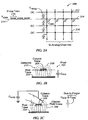
- FIG. 2a illustrates exemplary capacitive multi-touch panel 200.
- FIG. 2a indicates the presence of a stray capacitance Cstray at each pixel 202 located at the intersection of a row 204 and a column 206 trace (although Cstray for only one column is illustrated in FIG. 2 for purposes of simplifying the figure).
- FIG. 2a illustrates rows 204 and columns 206 as being substantially perpendicular, they need not be so aligned, as described above.
- Each of columns 206 may be selectively connectable to one or more analog channels (see analog channels 108 in FIG. 1 ).
- FIG. 2b is a side view of exemplary pixel 202 in a steady-state (no-touch) condition.
- an electric field of electric field lines 208 of the mutual capacitance between column 206 and row 204 traces or electrodes separated by dielectric 210 represents a signal capacitance Csig between the row and column electrodes and can cease a charge to be injected form a stimulated row to a column electrode.
- Csig is referenced to virtual ground, it also makes up a stray capacitance.
- a total stray capacitance of a column electrode can be the sum of all signal capacitances Csig between a given column and all row electrodes.
- FIG. 2c is a side view of exemplary pixel 202 in a dynamic (touch) condition.
- finger 212 has been placed near pixel 202.
- Finger 212 is a low-impedance object at signal frequencies, and represents an CA ground return path to via body capacitance Cbody.
- the body has a self-capacitance to ground Cbody, which is a function of, among other things, body size and geometry.
- finger 212 blocks some electric field lines 208 between the row and column electrodes (those fringing fields that exit the dielectric and pass through the air above the row electrode), those electric field lines are shunted to ground through the capacitance path inherent in the finger and the body, and as a result, the steady state signal capacitance Csig is reduced by Csig_sense.
- the combined body and finger capacitance act to reduce Csig by an amount ⁇ Csig (which can also be referred to herein as Csig_sense), and can act as a shunt or dynamic return path to ground, blocking some of the electric fields as resulting in a reduced net signal capacitance.
- the signal capacitance at the pixel becomes Csig - ⁇ Csig, where Csig represents the static (no touch) component and ⁇ Csig represents the dynamic (touch) component.
- Csig - ⁇ Csig may always be nonzero due to the inability of a finger, palm or other object to block all electric fields, especially those electric fields that remain entirely within the dielectric material.
- ⁇ Csig can be variable and representative of how completely the finger is pushing down on the panel (i.e. a range from "no-touch” to "full-touch”).
- Vstim signal 214 can be applied to a row in multi-touch panel 200 so that a change in signal capacitance can be detected when a finger, palm or other object is present.
- Vstim signal 214 can include one or more pulse trains 216 at a particular frequency, with each pulse train including of a number of pulses.
- pulse trains 216 are shown as square waves, other waveshapes such as sine waves can also be employed.
- a plurality of pulse trains 216 at different frequencies can be transmitted for noise reduction purposes to minimize the effect of any noise sources.
- Vstim signal 214 essentially injects a charge into the row via signal capacitance Csig, and can be applied to one row of multi-touch panel 200 at a time while all other rows are held at a DC level.
- the multi-touch panel may be divided into two or more sections, with Vstim signal 214 being simultaneously applied to one row in each section and all other rows in that region section held at a DC voltage.
- Each analog channel coupled to a column can provide a result representing a mutual capacitance between a row being stimulated and a column the row is connected to.
- this mutual capacitance is comprised of the signal capacitance Csig and any change Csig_sense in that signal capacitance due to the presence of a finger, palm or other body part or object.
- These column values provided by the analog channels may be provided in parallel while a single row is being stimulated, or may be provided in series. If all of the values representing the signal capacitances for the columns have been obtained, another row in multi-touch panel 200 can be stimulated with all others held at a DC voltage, and the column signal capacitance measurements can be repeated.
- a "snapshot" of all pixel values can be obtained for the entire multi-touch panel 200.
- This snapshot data can be initially saved in the multi-touch subsystem, and later transferred out for interpretation by other devices in the computing system such as the host processor. As multiple snapshots are obtained, saved and interpreted by the computing system, it is possible for multiple touches to be detected, tracked, and used to perform other functions.
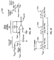
- FIG. 3a illustrates exemplary analog channel or event detection and demodulation circuit 300.
- One or more analog channels 300 can be present in the multi-touch subsystem.
- One or more columns from a multi-touch panel can be connectable to each analog channel 300.
- Each analog channel 300 can include virtual-ground charge amplifier 302, signal mixer 304, offset compensation 306, rectifier 332, subtractor 334, and analog-to-digital converter (ADC) 308.
- ADC analog-to-digital converter
- 3a also shows, in dashed lines, the steady-state signal capacitance Csig that can be contributed by a multi-touch panel column connected to analog channel 300 when an input stimulus Vstim is applied to a row in the multi-touch panel and no finger, palm or other object is present, and the dynamic signal capacitance Csig - ⁇ Csig that can appear when a finger, palm or other object is present.
- Vstim as applied to a row in the multi-touch panel, can be generated as a burst of square waves or other non-DC signaling in an otherwise DC signal, although in some embodiments the square waves representing Vstim can be preceded and followed by other non-DC signaling.
- the output of charge amplifier 302 can be pulse train 310 centered at Vref with a peak-to-peak (p-p) amplitude in the steady-state condition that is a fraction of the p-p amplitude of Vstim, the fraction corresponding to the gain of charge amplifier 302, which is equivalent to the ratio of signal capacitance Csig and preamplifier feedback capacitance Cfb.
- p-p peak-to-peak
- the output of the charge amplifier can be 1.8V p-p pulses.
- This output can be mixed in signal mixer 304 with demodulation waveform Fstim 316.
- the stimulation signal can be a square wave
- a Gaussian shaped sinewave In order to reduce the stop band ripple of the mixer at a given stimulation frequency, it can be advantageous to use a Gaussian shaped sinewave.
- the demodulation waveform can have the same frequency as the stimulus Vstim and can be synthesised from a Lookuptable, enabling generation of any shape of demodulation waveform.
- other waveshapes may be programmed to tune the filter characteristics of the mixers.
- Fstim 316 may be tunable in frequency and amplitude by selecting different digital waveforms in the LUT 312 or generating the waveforms differently using other digital logic.
- Signal mixer 304 may demodulate the output of charge amplifier 310 by subtracting Fstim 316 from the output to provide better noise rejection.
- Signal mixer 304 may reject all frequencies outside the passband, which may in one example be about +/- 30 kHz around Fstim. This noise rejection may be beneficial in noisy environment with many sources of noise, such as 802.11, Bluetooth and the like, all having some characteristic frequency that may interfere with the sensitive (femt-farad level) analog channel 300. Since the frequency of the signals going into the signal mixer can have the same frequency, the signal mixer may be thought of as a synchronous rectifier, such that the output of the signal mixer is essentially a rectified waveform.
- Offset compensation 306 can then be applied to signal mixer output 314, which can remove the effect of the static Csig, leaving only the effect of ⁇ Csig appearing as result 324.
- Offset compensation 306 can be implemented using offset mixer 330.
- Offset compensation output 322 can be generated by rectifying Fstim 316 using rectifier 332, and mixing rectifier output 336 with analog voltage from a digital-to-analog converter (DAC) 320 in offset mixer 330.
- DAC 320 can generate the analog voltage based on a digital value selected to increase the dynamic range of analog channel 300.
- Offset compensation output 322 which can be proportional to the analog voltage from DAC 320, can then be subtracted from signal mixer output 314 using subtractor 334, producing subtractor output 338 which can be representative of the change in the signal capacitance ⁇ Csig that occurs when a capacitive sensor on the row being stimulated has been touched.
- Subtractor output 338 is then integrated and can then be converted to a digital value by ADC 308.
- integrator and ADC functions are combined and ADC 308 may be an integrating ADC, such as a sigma-delta ADC, which can sum a number of consecutive digital values and average them to generate result 324.
- FIG. 3b is a more detailed view of charge amplifier (a virtual ground amplifier) 302 at the input of an analog channel, and the capacitance that can be contributed by the multi-touch panel (see dashed lines) and seen by the charge amplifier.
- charge amplifier a virtual ground amplifier
- Cstray capacitance there can be an inherent stray capacitance Cstray at each pixel on the multi-touch panel.
- the + (noninverting) input tied to Vref
- the - (inverting) input is also driven to Vref, and a DC operating point is established. Therefore, regardless of how much Csig is present, the - input is always driven to Vref.
- the gain of virtual ground amplifier 302 is usually small (e.g. 0.1) and is equivalent to the ratio of Csig (e.g. 2 pF) and feedback capacitor Cfb (e.g. 20 pF).
- the adjustable feedback capacitor Cfb converts the charge Qsig to the voltage Vout. Therefore, the output Vout of virtual ground amplifier 302 is a voltage that is equivalent to the ratio of-Csig/Cfb multiplied by Vstim referenced to Vref.
- the high voltage Vstim pulses can therefore appear at the output of virtual ground amplifier 302 as much smaller pulses having an amplitude identified by reference character 326.
- the amplitude of the output can be reduced as identified by reference character 328, because the signal capacitance is reduced by ⁇ Csig.
- channels (e.g., rows) of the multi-touch panel may be stimulated with a plurality of pulse train bursts.
- the frequency of the pulse trains may vary from one to the other.
- Figure 3c illustrates an exemplary stimulation signal Vstim with multiple pulse trains 330a, 330b, 330c, each of which have a fixed number of pulses, but have a different frequency Fstim (e.g. 140 kHz, 200 kHz, and 260 kHz).
- Fstim frequency
- a different result may be obtained at each frequency.
- a static interference is present at a particular frequency
- the results of a signal at that frequency may be corrupted as compared to the results obtained from signals having other frequencies.
- the corrupted result or results can be eliminated and the remaining results used to compute a final result or, alternatively, all of the results may be used.
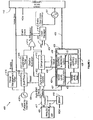
- system 100 includes auto-scan logic.
- Auto-scan logic may reside in channel scan logic block 110 of multi-touch subsystem 106, separately from channel scan logic 110 in multi-touch subsystem 106, or entirely separate from multi-touch subsystem 106.
- auto-scan logic can autonomously read data from analog channels 108 and provide control of analog channels 108. This is referred to as "auto-scan mode.” Accordingly, auto-scan mode enables the system 100 to scan multi-touch panel 124 without intervention from multi-touch processor 102 and while one or more system clocks are disabled. This allows multi-touch system 100 to conserve power or free up components (such as processor 102) to perform other tasks while the system is in auto-scan mode.
- a user may not be continuously inputting data into touch panel 124, it may be desirable to initiate auto-scan mode after a predetermined amount of time has transpired without the system 100 sensing any touch-events. By doing so, the system 100 can conserve power while no data is being inputted (because auto-scan mode is enabled), but power back up once the user resumes inputting data.
- FIG. 4 is a block diagram of one embodiment of auto-scan logic 400.
- auto-scan logic 400 can include auto-scan control 402, which can control row address and channel timing functions, among other things.
- auto-scan control 402 can include a row address state machine and a channel timing state machine for controlling scanning multi-touch panel 124.
- the various functions and components of auto-scan control 402 can be shared with or overlap with channel scan logic 110 and driver logic 114.
- sniff timer 404 and calibration timer 406 can be clocked by oscillator 408.
- Oscillator can be a low frequency oscillator or high frequency oscillator; however, for power conservation reasons, a low frequency oscillator may be desirable.
- Low frequency oscillator can reside in the multi-touch subsystem 106, or can reside outside of multi-touch subsystem 106.
- sniff timer 404 After a predetermined amount of time (referred to as "sniff time"), sniff timer 404 initiates scan sequence.
- autoscan mode can be comprised to two individual system states: an actual sniff interval during which only a low frequency oscillator and a sniff time is active, and a scan sequence in which a multi-touch panel is actively scanned. The two system states may form the auto-scan mode.
- high frequency oscillator 421 wakes up instantaneously. The faster the high frequency oscillator wakes up the less time the system spends actively scanning the panel. Further details concerning a high frequency oscillator are described in US 2008/0157882 entitled "Automatic Frequency Calibration".
- high frequency oscillator 421 is a fast startup oscillator that allows fast lock after the system wakes up from a lower power management state to scan the multi-touch panel. To reduce the time between wake- up, scanning the multi-touch panel and going back into a lower power state, it may be advantageous for the oscillating signal to become stable in a relatively short period in order to minimize the time the system is active and thus to conserve power. Many crystal oscillators may take several milliseconds to stabilize. However, a fast start-up oscillator circuit can stabilize within tens of microseconds, thus enabling the system to go back into a lower power management state much faster than, for example, a system that is driven by a slower stabilizing crystal oscillator.
- an auto-scan process can be enabled by first enabling auto-scan control 402 and then putting the processor into a wait for interrupt state.
- Clock manager 414 then shuts down high frequency oscillator 421 and initiates the sniff timer 404, which after a sniff timeout, causes clock manager 414 to enable high frequency oscillator 421 and then sends a request to the channel scan logic 110 to perform a scan, but keeping the processor inactive.
- Channel scan logic 110 then acquires a multi-touch image on pixel locations that can be specified through programming appropriate registers. Multi-touch image results from analog channels 430 (which may be analog channel 300 of Figure 3A ) may be subtracted in subtractor 417 by a baseline image stored in baseline RAM 419.
- the subtracted result can then be compared to a threshold value by comparator 410. If the resulting value is above the programmable threshold value, an interrupt is set and the processor is woken up. If the resulting value is below the threshold value, then the system remains in autoscan mode until either a calibration time expires or an external interrupt occurs.
- an auto-scan mode permits multi-touch data input to be read from multi-touch panel 124 while the processor is inactive.
- sniff timer 404 is reset each time sniff timer initiates an auto-scan sequence.
- the sniff time can be in the range of 8 milliseconds to 2 seconds, for example 50 milliseconds.
- Calibration timer 406 can wake up processor 102 when auto-scan logic 400 stays in auto-scan mode for an extended amount of time without any touch events detected on touch panel 124 exceeding a threshold, as discussed in more detail below.
- the calibration timer 406 initiates a "calibration" upon expiration of a predetermined amount of time ("calibration time”).
- a "calibration” can include waking up the high frequency oscillator and activating the system clock and processor 102 to perform a scan of the multi-touch panel 102.
- the calibration can also include calibration functions, such as accounting for any drift in the sensor panel 124.
- the calibration time is greater than the sniff time and can be in the range of 2 seconds to 300 seconds.
- comparator 410 compares offset compensated results with a threshold value as described above. In one embodiment, if the threshold value is exceeded, then one or more touch events detected on the panel 124 have occurred that take the system 100 out of auto-scan mode and into active scan mode. The comparison of the threshold value with the compensated results can be done on a channel-by-channel, row-by-row basis. In one embodiment, the threshold value can be programmed into a threshold value register.
- OR gate 412 can be included between the output paths of calibration timer 406 and comparator 410. Accordingly, when either the calibration time of calibration timer 406 or the threshold value of comparator 410 is exceeded, OR gate can initiate sending an interrupt signal to processor 102 and clock manger 414 for the purpose of re-enabling processor 102 and clocks.
- Clock manager 414 can control one or more clocks in system 100. In general, when any clocks are not needed at a given time, clock manager 414 can disable those clocks so as to conserve power, and when any disabled clocks are needed, clock manager 414 can enable those clocks. In one embodiment, clock manager 414 can control low frequency oscillator 408, the high frequency oscillator (not shown) and the system clock (not shown) clocking processor 102.
- Power management timer 416 can be included in auto-scan logic 400. Power management timer 416 counts up to a time equal to the sniff time less a delay time.
- the delay time can be the amount of time needed for the multi-touch system 100 to get ready to perform a scan, "settle" high voltage drivers 118 (i.e. to provide a stable supply of voltage) prior to performing a scan.
- the delay time can be adjusted via a power manager register, and can be different for each channel 108 that is scanned.
- noise management block 424 can be included. False wakeups can cause a processor to exit the wait for interrupt state and actively scan the panel. Moreover, repetitive false triggers can cause the overall power consumption of a system to increase substantially. Noise management block 424 can advantageously discern whether a threshold value was exceeded due to, for example, a finger touching the panel or due to noise corrupting one of the scan frequencies.
- auto-scan logic 400 may scan at more than one frequency and transfer the resulting data to noise management block 424.
- Noise calculation block 427 can calculate the noise levels based on a history of result data acquired for different scan frequencies and uses noise level RAM 425 to keep a history of noise levels and associated frequencies.
- Control and decision logic 428 can compare ADC results acquired for one row scan at different frequencies. If, for example, if ADC result data for the scan frequencies track each other within a certain window, then it is likely that a touch condition caused the threshold to be exceeded as a touch condition, as a touch would affect the result values for all of the scan frequencies.
- the control and decision logic 428 could generate a holdoff signal 435 to prevent the comparator 410 from generating a processor interrupt. If a noisy frequency channel is detected, that frequency can be removed from the frequency hopping table 426 and IO block 429.
- the frequency hopping table 426 may contain data representing clean frequency channels and may be programmed during factory calibration.
- IO block 429 can send a new set of scan frequency data to channel timing logic 110. The frequency data can determine the scan frequencies for the next channel timing sequence. Periodically changing the scan frequencies based on the noise environment make the auto-scan logic 400 more robust, which can ultimately aid in the reduction of power.
- charge amplifiers in each analog channel 430 can be configured to operate in stray capacitance mode.
- channel scan logic 110 can initiate a stray capacitance mode by sending a stray capacitance mode initiate signal to analog channels 430. Initiating stray capacitance measurements of a multi-touch panel device is discussed in further detail in US 7986313B2 entitled "Analog Boundary Scanning Based on Stray Capacitance".
- using the stray capacitance mode does not provide an accurate location of where a touch event occurred on the panel 124, as the stray capacitance mode provides only an indication that one or more touch events occurred on or near one of the columns being scanned.
- using the stray capacitance mode can be advantageous because only one scan is needed to determine if a touch event occurred on the multi-touch panel 124; as opposed to a plurality of scans that may be needed using the mutual capacitance mode. Accordingly, using fewer scans can significantly reduce the amount of power consumed to scan the panel 124. For example, in one implementation, it was found that a scan using the stray capacitance mode uses about the same amount of power as the amount of power dissipated due to the leakage current present in a multi-touch system.
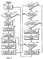
- An exemplary auto-scan process 500 in accordance with one embodiment is illustrated in the flowchart of Figure 5 .
- One skilled in the art will appreciate that various timing and memory storage issues are omitted from this flowchart for the sake of clarity.
- the auto-scan process 500 begins with system 100 in active scan mode in block 502.
- processor 102 is enabled and system 100 is actively scanning the multi-touch panel 124.
- process 500 determines whether sufficient touch events have taken place on the touch panel within a predetermined amount of time (e.g., in the range of 1ms to a number of minutes) in block 504. This decision can be performed by, for example, processor 102. Alternatively, a separate processor or dedicated logic, such as channel scan logic 110, can perform this task. If it is found that there has been sufficient touch activity, then process 500 returns to block 502 and the system 100 remains in active scan mode. If, on the other hand, it is determined that there has not been a sufficient touch activity, then auto-scan mode is enabled in block 506.
- auto-scan mode can be enabled by processor 102 sending an auto-scan enable signal to auto-scan control 402.
- auto-scan mode can be enabled by having processor 102 set an auto-scan enable bit in an auto-scan register, which is monitored by auto-scan control 402. Further variations of enabling auto-scan mode may also be used, as is appreciated by one skilled in the art.
- auto-scan logic 400 can disable one or more of these components via clock manager 414.
- sniff timer 404 is activated and reset (block 514) as well as calibration timer 406 (block 516).
- the activation and resetting functions can be initiated by auto-scan control 402.
- Process 500 then proceeds to decision block 518 to determine whether an interrupt signal has been received, such as a signal from comparator 410 indicating that a threshold has been exceeded. If an interrupt has been received, then any clocks that were turned off during auto-scan mode are turned on and the processor 102 is enabled (block 520). Process 500 then returns to active scanning mode in block 502.
- process 500 determines if sniff timer 604 exceeded the sniff time (block 522). If the sniff time is not exceeded, then process 500 returns to block 518. If the sniff time is exceeded, then process 500 determines if calibration timer 406 exceeded the calibration time (block 520). If the calibration time is exceeded, then the clocks and processor are enabled (block 514) and active scan mode is enabled (block 502).
- the high frequency oscillator is woken up (i.e., enabled) in block 526 and an image of the multi-touch panel 124 is acquired (block 528).
- Various implementations can be used to acquire an image in block 524, which are discussed in more detail further below.
- the image acquired in block 524 is done while processor 102 is disabled.
- process 500 determines if a programmable threshold is exceeded (block 530). This can be done by comparing offset compensated results 324 received from ADC 308 ( Figure 3a ) with the threshold value. If the threshold is exceeded, then the clocks and processor 102 are enabled (block 514) and the process 500 returns to active scan mode (block 502). If the threshold is not exceeded, then process 500 returns to the block 512 (turning off the high frequency clock).
- an image may be acquired measuring either a mutual capacitance or a stray capacitance.
- system 100 When measuring mutual capacitance (which may be referred to as "mutual capacitance mode"), system 100 detects changes in capacitance at each node of the multi-touch panel, as described above with reference to Figures 3b and 3c . Accordingly, to acquire an image of multi-touch panel 124 using the mutual capacitance mode, each row is typically scanned. In alternative embodiments, only select rows are scanned to conserve energy. For example, scanning every other row, or scanning rows located on a certain area of multi-touch panel 124, such as a top, bottom or middle area of the multi-touch panel. In further embodiments, select frames of multi-touch panel 124 are scanned using mutual capacitance mode.
- measuring stray capacitance can be used (which may be referred to as "stray capacitance mode") instead of or in combination with the mutual capacitance mode.
- stray capacitance mode can measure the output of all columns of the multi-touch panel 124 in one scan.
- FIG. 6 is a power management profile 600 of an auto-scan cycle in accordance with one embodiment of the invention.
- One complete auto-scan cycle can be, for example, 50 ms.
- sniff mode very little power is used, as only low frequency clock 408, sniff timer 404 and calibration timer 406 are active. After the sniff time is exceeded, an auto-scan is performed, which is shown as a period of scan activity in Figure 6 .
- multi-touch panel 124 is scanned without intervention from processor 102.
- low frequency clock 404, high frequency clock, auto-scan control 402 and other components needed perform an auto-scan are powered. This results in more power consumption than occurs during the sniff time, but less than if processor 102 and other clocks were active (e.g., during active scan mode).
- one or more rows of multi-touch panel 124 may be scanned. In one implementation, 48 rows are scanned, each row scan taking about .1 ms to perform. Accordingly, it takes a total of about 4.8 ms to scan every row. If stray capacitance mode is used, then only one scan needs to be performed. This scan takes about. .1 ms to perform. Thus, using stray capacitance mode can be faster (.1 ms as opposed to 4.8 ms in this example) and can also use less power (about 2% of the power used in the mutual capacitance mode described in this example).
- the hybrid mode can include initially using the stray capacitance mode to detect a touch event on the multi-touch panel 124 and, if a touch event is detected, then using the mutual capacitance mode to provide an accurate location of where the touch event occurred.
- the touch event can be required to happen in a predetermined manner in order to exceed the threshold.
- the system may require simultaneous or nearly simultaneous touch events to occur in particular locations or in a particular manner (e.g., a simulated dial turning motion). If the threshold is not exceeded, then the auto-scan mode can continue as described in process 500 (e.g., return to block 512).
- auto-scan mode scans at a single frequency band. This may conserve power. Alternatively, auto-scan mode can scan at multiple different frequencies as described with reference to Figure 3c .
- auto-scan logic includes a noise management block.
- the noise management block prevents waking up the processor in cases where threshold levels are exceeded due to presence of noise not because of the user not touching the multi-touch screen. By remaining in auto-scan mode, power is saved.
- the noise management block can take a survey of noise levels for several channels. If one channel has excessive Csig readings then it is likely an interferer on that channel. If the readings of all channels are the same then it is likely a user touching the panel. Dependent on the noise levels the noise management block provides a frequency-hopping table back to the channel scan logic with frequencies on clean channels.
- the noise management clock also includes a calibration engine to recalibrate the internal high frequency oscillator to prevent oscillator drift into a noisy channel.
- Figure 7 illustrates an exemplary mobile (e.g., cellular) telephone 736 that can include multi-touch panel 724, display device 730, and other computing system blocks in the computing system 100 of Figure 1 .
- computing system 100 may determine that mobile telephone 736 is being held up to the user's head, and therefore some or all of multi-touch subsystem 106 and multi-touch panel 724 can be powered down along with display device 730 to save power.
- Figure 8 illustrates an exemplary digital audio/video player that can include multi-touch panel 824, display device 830, and other computing system blocks in the computing system 100 of Figure 1 .
- proximity sensor panels which sense “hover” events or conditions, may also be used to generate modulated output signals for detection by the analog channels.
- Proximity sensor panels are described in US 9250734 B2 entitled “Proximity and Multi-Touch Sensor Detection and Demodulation”.
- touch events or conditions should be construed to encompass “hover” events and conditions and may collectively be referred to as “events.”
- touch surface panels should be construed to encompass “proximity sensor panels.”
Landscapes
- Engineering & Computer Science (AREA)
- Theoretical Computer Science (AREA)
- General Engineering & Computer Science (AREA)
- Physics & Mathematics (AREA)
- General Physics & Mathematics (AREA)
- Human Computer Interaction (AREA)
- Position Input By Displaying (AREA)
- Power Sources (AREA)
Claims (13)
- Auto-Scan-Logikschaltung, die betriebsbereit mit einem Sensorfeld verbindbar ist, welches zumindest einen Erfassungsknoten aufweist, der ein Ausgabesignal bereitstellt, welches hinweisend ist auf ein Vorhandensein oder eine Abwesenheit eines Ereignisses, welches an dem Sensorfeld auftritt,
wobei die Auto-Scan-Logikschaltung konfiguriert ist, um eine Berührungserfassung zu deaktivieren nachdem eine erste vorbestimmte Zeitmenge abgelaufen ist, in der kein Ereignis an dem Sensorfeld erfasst wurde, die Berührungserfassung zu aktivieren und das Sensorfeld zu scannen, wenn die Berührungsoberflächenvorrichtung in dem Auto-Scan-Modus ist nach einem Ablaufen einer zweiten vorbestimmten Zeitmenge, und um zu bestimmen, ob irgendein Ereignis auf dem Sensorfeld erfasst wird. - Auto-Scan-Logikschaltung nach Anspruch 1, ferner konfiguriert zum Eintreten in einen Auto-Scan-Modus, wenn kein Ereignis auf dem Sensorfeld für eine vorbestimmte Zeitmenge erfasst wird.
- Auto-Scan-Logikschaltung nach Anspruch 1, die einen Sniff-Timer umfasst, wobei der Sniff-Timer einen Scan-Vorgang des Sensorfeldes initiiert zum Bestimmen eines Vorhandenseins oder einer Abwesenheit eines Ereignisses, welches an dem Sensorfeld auftritt, wenn der Sniff-Timer die zweite vorbestimmte Zeitmenge erreicht.
- Auto-Scan-Logikschaltung nach Anspruch 3, die ferner einen Kalibrierungs-Timer umfasst, wobei der Kalibrierungs-Timer automatisch einen Scan-Vorgang initiiert, wenn der Kalibrierungs-Timer eine dritte vorbestimmte Zeitmenge erreicht, welche größer ist als die zweite vorbestimmte Zeitmenge.
- Auto-Scan-Logikschaltung nach Anspruch 4, wobei der Kalibrierungs-Timer eine Kalibrierungssequenz initiiert, welche Abweichung berücksichtigt, die in dem Sensorfeld vorhanden ist.
- Auto-Scan-Logikschaltung nach Anspruch 3, die einen Leistungsverwaltungs-Timer umfasst, wobei der Leistungsverwaltungs-Timer ein Hochfahrsignal an einen oder mehrere Spannungstreiber sendet bevor der Sniff-Timer die zweite vorbestimmte Zeitmenge erreicht.
- Auto-Scan-Logikschaltung nach Anspruch 1, die ferner einen Taktverwalter umfasst, der in der Lage ist, einen oder mehrere Takte, die in der Berührungsoberflächenvorrichtung vorhanden sind, zu deaktivieren und zu aktivieren.
- Verfahren zum Scannen eines Sensorfeldes, umfassend:Initiieren eines Auto-Scan-Modus nachdem ein oder mehrere Berührungsereignisse nicht auf einem Sensorfeld für eine erste vorbestimmte Zeitmenge erfasst wurden, wobei der Auto-Scan-Modus umfasst:Deaktivieren eines Sensorfeldprozessors;Aktivieren von Berührungserfassung und Durchführen eines Sniff-Scan-Vorgangs, wenn eine zweite vorbestimmte Zeitmenge abgelaufen ist, die geringer ist als eine dritte vorbestimmte Zeitmenge; undDurchführen eines Kalibrierungs-Scan-Vorgangs, wenn die dritte vorbestimmte Zeitmenge abgelaufen ist; undBestimmen, ob irgendein Ereignis auf dem Sensorfeld erfasst wird.
- Verfahren nach Anspruch 8, wobei das Durchführen des Sniff-Scan-Vorgangs umfasst:Scannen des Feldes auf ein Vorhandensein oder eine Abwesenheit eines Ereignisses an dem Sensorfeld;Erzeugen von einem oder mehreren Werten, die repräsentativ für Ereignisse sind, die an unterschiedlichen Orten auf dem Feld auftreten; undVergleichen des einen oder der mehreren Werte mit einem Schwellwert und Aktivieren des Sensorfeldprozessors, wenn der eine oder die mehreren Werte den Schwellwert überschreiten.
- Verfahren nach Anspruch 9, wobei der Schritt zum Erzeugen von einem oder mehreren Werten Messen eines Streukapazitätswertes oder eines Gegenkapazitätswertes von einem oder mehreren Berührungssensoren in dem Sensorfeld umfasst.
- Verfahren nach Anspruch 8, wobei der Kalibrierungs-Scan-Vorgang umfasst:Aktivieren des Sensorfeldprozessors;Scannen des Sensorfeldes auf ein Vorhandensein oder eine Abwesenheit eines Ereignisses an dem Feld; undDurchführen einer Kalibrierung, um Abweichung zu berücksichtigen, die in dem Sensorfeld vorhanden ist.
- Berührungsoberflächenvorrichtung, umfassend:ein Sensorfeld, welches zumindest einen Erfassungsknoten aufweist, welcher ein Ausgabesignal bereitstellt, das hinweisend auf ein Vorhandensein oder eine Abwesenheit eines Ereignisses ist, welches an dem Sensorfeld auftritt;einen Prozessor, der betriebsbereit mit dem Sensorfeld verbunden ist, wobei der Prozessor in der Lage ist zum Verarbeiten des Ausgabesignals des Sensorfeldes, wenn die Berührungsoberflächenvorrichtung in einem aktiven Scan-Modus ist, und deaktiviert ist, wenn die Berührungsoberflächenvorrichtung in einem Auto-Scan-Modus ist; undein Mehrfachberührungsuntersystem zum Erfassen von Ereignissen auf oder um eine Sensoroberfläche und Erzeugen eines Bildes der Ereignisse umfassend:Treiberlogik, die konfiguriert ist zum Erzeugen eines oder mehrerer Eingangsstimuli;Kanal-Scan-Logik, die konfiguriert ist zum Steuern der Treiberlogik, um eine oder mehrere Reihen von Sensoren in einem Sensorfeld zu scannen durch Treiben von zumindest einer Reihe mit dem einen oder den mehreren Eingangsstimuli;einen oder mehrere Analogkanäle, wobei jeder Analogkanal mit einer Spalte von Sensoren in dem Sensorfeld koppelbar ist, wobei jeder Analogkanal konfiguriert ist zum Empfangen eines Signals, welches repräsentativ für ein Ereignis ist, welches an einem der Sensoren in der Spalte von Sensoren auftritt, und Erzeugen eines Wertes, der repräsentativ für das Ereignis ist; undeine Auto-Scan-Logikschaltung nach irgendeinem der Ansprüche 1 bis 7.
- Berührungsvorrichtung nach Anspruch 12, ferner umfassend ein Rechensystem, welches die Berührungsfeldvorrichtung beinhaltet, wobei das Rechensystem in einem mobilen Telefon oder einem digitalen Audiospieler beinhaltet ist, der das Rechensystem beinhaltet.
Priority Applications (1)
| Application Number | Priority Date | Filing Date | Title |
|---|---|---|---|
| EP17170603.9A EP3252582B1 (de) | 2007-01-03 | 2007-12-22 | Automatische mehrfachabtastung |
Applications Claiming Priority (2)
| Application Number | Priority Date | Filing Date | Title |
|---|---|---|---|
| US11/650,040 US8125456B2 (en) | 2007-01-03 | 2007-01-03 | Multi-touch auto scanning |
| PCT/US2007/088751 WO2008085720A1 (en) | 2007-01-03 | 2007-12-22 | Multi-touch auto scanning |
Related Child Applications (1)
| Application Number | Title | Priority Date | Filing Date |
|---|---|---|---|
| EP17170603.9A Division EP3252582B1 (de) | 2007-01-03 | 2007-12-22 | Automatische mehrfachabtastung |
Publications (3)
| Publication Number | Publication Date |
|---|---|
| EP2118726A1 EP2118726A1 (de) | 2009-11-18 |
| EP2118726A4 EP2118726A4 (de) | 2012-03-07 |
| EP2118726B1 true EP2118726B1 (de) | 2017-05-17 |
Family
ID=39052585
Family Applications (2)
| Application Number | Title | Priority Date | Filing Date |
|---|---|---|---|
| EP07866002.4A Active EP2118726B1 (de) | 2007-01-03 | 2007-12-22 | Mehrfach-berührungs-auto-scanning |
| EP17170603.9A Active EP3252582B1 (de) | 2007-01-03 | 2007-12-22 | Automatische mehrfachabtastung |
Family Applications After (1)
| Application Number | Title | Priority Date | Filing Date |
|---|---|---|---|
| EP17170603.9A Active EP3252582B1 (de) | 2007-01-03 | 2007-12-22 | Automatische mehrfachabtastung |
Country Status (10)
| Country | Link |
|---|---|
| US (6) | US8125456B2 (de) |
| EP (2) | EP2118726B1 (de) |
| JP (4) | JP5786239B2 (de) |
| KR (1) | KR101109346B1 (de) |
| CN (2) | CN101583923B (de) |
| AU (2) | AU2007342148B2 (de) |
| DE (1) | DE202007018133U1 (de) |
| HK (1) | HK1108274A2 (de) |
| TW (2) | TWM341273U (de) |
| WO (1) | WO2008085720A1 (de) |
Families Citing this family (244)
| Publication number | Priority date | Publication date | Assignee | Title |
|---|---|---|---|---|
| US8094128B2 (en) * | 2007-01-03 | 2012-01-10 | Apple Inc. | Channel scan logic |
| US7812827B2 (en) | 2007-01-03 | 2010-10-12 | Apple Inc. | Simultaneous sensing arrangement |
| US8125456B2 (en) | 2007-01-03 | 2012-02-28 | Apple Inc. | Multi-touch auto scanning |
| US7986313B2 (en) * | 2007-01-03 | 2011-07-26 | Apple Inc. | Analog boundary scanning based on stray capacitance |
| US8525799B1 (en) * | 2007-04-24 | 2013-09-03 | Cypress Semiconductor Conductor | Detecting multiple simultaneous touches on a touch-sensor device |
| US8144126B2 (en) * | 2007-05-07 | 2012-03-27 | Cypress Semiconductor Corporation | Reducing sleep current in a capacitance sensing system |
| US8253425B2 (en) * | 2007-05-08 | 2012-08-28 | Synaptics Incorporated | Production testing of a capacitive touch sensing device |
| US9229549B1 (en) * | 2007-05-29 | 2016-01-05 | Cypress Semiconductor Corporation | Random scanning technique for secure transactions entered with capacitive sensor input device |
| US8493331B2 (en) | 2007-06-13 | 2013-07-23 | Apple Inc. | Touch detection using multiple simultaneous frequencies |
| KR20090030902A (ko) * | 2007-09-21 | 2009-03-25 | 엘지전자 주식회사 | 식기세척기의 입력장치 및 그 제어방법, 세탁장치의입력장치 및 그 제어방법 |
| US8633915B2 (en) | 2007-10-04 | 2014-01-21 | Apple Inc. | Single-layer touch-sensitive display |
| WO2009070814A2 (en) * | 2007-11-27 | 2009-06-04 | Frederick Johannes Bruwer | Capacitive sensing circuit with noise rejection |
| US20090174676A1 (en) | 2008-01-04 | 2009-07-09 | Apple Inc. | Motion component dominance factors for motion locking of touch sensor data |
| US9372576B2 (en) * | 2008-01-04 | 2016-06-21 | Apple Inc. | Image jaggedness filter for determining whether to perform baseline calculations |
| US10969917B2 (en) * | 2008-01-30 | 2021-04-06 | Apple Inc. | Auto scanning for multiple frequency stimulation multi-touch sensor panels |
| US8154310B1 (en) * | 2008-02-27 | 2012-04-10 | Cypress Semiconductor Corporation | Capacitance sensor with sensor capacitance compensation |
| US9329732B2 (en) * | 2008-03-19 | 2016-05-03 | Egalax—Empia Technology Inc. | Device and method for detecting touch screen |
| US20160209963A1 (en) * | 2008-03-19 | 2016-07-21 | Egalax_Empia Technology Inc. | Touch processor and method |
| US8619055B2 (en) * | 2008-04-14 | 2013-12-31 | Microsoft Corporation | Active matrix touch sensing |
| US20090273577A1 (en) * | 2008-04-30 | 2009-11-05 | Apple Inc. | Moire-Free Touch Screen with Tilted or Curved ITO Pattern |
| DE112009001503T5 (de) | 2008-06-20 | 2011-04-28 | Mattel, Inc., El Segundo | Kapazitives Tastfeld und Spielzeug, das ein solches enthält |
| DE102008032451C5 (de) * | 2008-07-10 | 2017-10-19 | Rational Ag | Anzeigeverfahren und Gargerät hierfür |
| TW201007526A (en) * | 2008-08-13 | 2010-02-16 | Elan Microelectronics Corp | Signal processing method of multi-fingers touch apparatus having invisible physical button structure |
| US20100060611A1 (en) * | 2008-09-05 | 2010-03-11 | Sony Ericsson Mobile Communication Ab | Touch display with switchable infrared illumination for touch position determination and methods thereof |
| TWI484392B (zh) * | 2008-09-23 | 2015-05-11 | Holtek Semiconductor Inc | 觸碰面板的判讀方法與裝置 |
| US8363031B2 (en) * | 2008-09-24 | 2013-01-29 | 3M Innovative Properties Company | Mutual capacitance measuring circuits and methods |
| JP5324297B2 (ja) * | 2009-04-15 | 2013-10-23 | 株式会社ジャパンディスプレイ | 座標入力装置、およびそれを備える表示装置 |
| US8330474B2 (en) * | 2008-10-15 | 2012-12-11 | Synaptics Incorporated | Sensor device and method with at surface object sensing and away from surface object sensing |
| JP5087792B2 (ja) * | 2008-10-31 | 2012-12-05 | 株式会社ワコム | 位置検出装置 |
| US8487639B1 (en) | 2008-11-21 | 2013-07-16 | Cypress Semiconductor Corporation | Receive demodulator for capacitive sensing |
| US9075457B2 (en) * | 2008-12-12 | 2015-07-07 | Maxim Integrated Products, Inc. | System and method for interfacing applications processor to touchscreen display for reduced data transfer |
| US10585493B2 (en) | 2008-12-12 | 2020-03-10 | Apple Inc. | Touch sensitive mechanical keyboard |
| TWI376624B (en) * | 2008-12-23 | 2012-11-11 | Integrated Digital Tech Inc | Force-sensing modules for light sensitive screens |
| KR101572071B1 (ko) | 2009-01-06 | 2015-11-26 | 삼성전자주식회사 | 휴대단말 표시부의 온/오프 제어 방법 및 장치 |
| US8552957B2 (en) * | 2009-02-02 | 2013-10-08 | Apple Inc. | Liquid crystal display reordered inversion |
| US8760412B2 (en) * | 2009-02-02 | 2014-06-24 | Apple Inc. | Dual configuration for display data lines |
| US8922521B2 (en) | 2009-02-02 | 2014-12-30 | Apple Inc. | Switching circuitry for touch sensitive display |
| TWI488095B (zh) * | 2009-02-26 | 2015-06-11 | Genesys Logic Inc | 省電之表面電容式觸控面板裝置以及其方法 |
| US8860687B2 (en) * | 2009-02-27 | 2014-10-14 | Japan Display, Inc. | Display, touch panel and electronic device |
| US20110157068A1 (en) * | 2009-12-31 | 2011-06-30 | Silicon Laboratories Inc. | Touch screen power-saving screen scanning algorithm |
| US8866500B2 (en) * | 2009-03-26 | 2014-10-21 | Cypress Semiconductor Corporation | Multi-functional capacitance sensing circuit with a current conveyor |
| US8982051B2 (en) * | 2009-03-30 | 2015-03-17 | Microsoft Technology Licensing, Llc | Detecting touch on a surface |
| US9317140B2 (en) * | 2009-03-30 | 2016-04-19 | Microsoft Technology Licensing, Llc | Method of making a multi-touch input device for detecting touch on a curved surface |
| US8593410B2 (en) | 2009-04-10 | 2013-11-26 | Apple Inc. | Touch sensor panel design |
| TWI402737B (zh) * | 2009-05-04 | 2013-07-21 | Mitac Int Corp | Multi - touch device and its method |
| US9804213B2 (en) * | 2009-05-13 | 2017-10-31 | Synaptics Incorporated | Capacitive sensor device |
| KR101752015B1 (ko) | 2009-05-29 | 2017-06-28 | 쓰리엠 이노베이티브 프로퍼티즈 컴파니 | 고속 멀티-터치 터치 디바이스 및 그 제어기 |
| TWI399684B (zh) * | 2009-06-18 | 2013-06-21 | Raydium Semiconductor Corp | 觸控輸入裝置與觸控感測電路 |
| JP5396167B2 (ja) * | 2009-06-18 | 2014-01-22 | 株式会社ワコム | 指示体検出装置及び指示体検出方法 |
| JP5295008B2 (ja) * | 2009-06-18 | 2013-09-18 | 株式会社ワコム | 指示体検出装置 |
| US8436822B2 (en) * | 2009-06-24 | 2013-05-07 | Himax Technologies Limited | Touch panel |
| TWI528250B (zh) * | 2009-06-25 | 2016-04-01 | Elan Microelectronics Corp | Object Detector and Method for Capacitive Touchpad |
| US9606667B2 (en) | 2009-06-29 | 2017-03-28 | Japan Display Inc. | Method of driving touch panel, capacitance-type touch panel, and display apparatus with touch detection function |
| JP5191452B2 (ja) | 2009-06-29 | 2013-05-08 | 株式会社ジャパンディスプレイウェスト | タッチパネルの駆動方法、静電容量型タッチパネルおよびタッチ検出機能付き表示装置 |
| US8957874B2 (en) | 2009-06-29 | 2015-02-17 | Apple Inc. | Touch sensor panel design |
| US20100328229A1 (en) * | 2009-06-30 | 2010-12-30 | Research In Motion Limited | Method and apparatus for providing tactile feedback |
| JP5086394B2 (ja) * | 2009-07-07 | 2012-11-28 | ローム株式会社 | タッチパネルの制御回路、制御方法およびそれらを用いたタッチパネル入力装置、電子機器 |
| TWI450138B (zh) * | 2009-07-15 | 2014-08-21 | Innolux Corp | 觸控面板及其多點辨識方法 |
| TWI427518B (zh) * | 2009-08-06 | 2014-02-21 | Raydium Semiconductor Corp | 觸控感測電路及觸控感測方法 |
| TWI393042B (zh) * | 2009-08-11 | 2013-04-11 | Au Optronics Corp | 具高觸碰靈敏度之觸碰面板裝置與其觸碰定位方法 |
| TWI400646B (zh) | 2009-08-12 | 2013-07-01 | Htc Corp | 觸控感測元件之壓力偵測方法以及使用該方法之電子裝置 |
| CN102473059B (zh) * | 2009-08-12 | 2015-06-24 | 瑟克公司 | 用于触摸板多触点感应的同步定时正交测量模式 |
| TWI431520B (zh) * | 2009-08-14 | 2014-03-21 | Elan Microelectronics Corp | Front - end signal detectors and methods for improving the anti - noise capability of capacitive touch panels |
| KR100941927B1 (ko) * | 2009-08-21 | 2010-02-18 | 이성호 | 터치입력 인식방법 및 장치 |
| US8334849B2 (en) * | 2009-08-25 | 2012-12-18 | Pixart Imaging Inc. | Firmware methods and devices for a mutual capacitance touch sensing device |
| TWI473490B (zh) * | 2009-09-03 | 2015-02-11 | Htc Corp | 調整事件提示程度的方法與其行動電子裝置及電腦程式產品 |
| US8970506B2 (en) | 2009-09-11 | 2015-03-03 | Apple Inc. | Power management for touch controller |
| US9036650B2 (en) * | 2009-09-11 | 2015-05-19 | Apple Inc. | Automatic low noise frequency selection |
| CN102025822B (zh) * | 2009-09-16 | 2017-05-31 | 宏达国际电子股份有限公司 | 调整事件提示程度的方法与其移动电子装置 |
| US9753586B2 (en) * | 2009-10-08 | 2017-09-05 | 3M Innovative Properties Company | Multi-touch touch device with multiple drive frequencies and maximum likelihood estimation |
| CN102043506B (zh) * | 2009-10-09 | 2013-07-17 | 禾瑞亚科技股份有限公司 | 分析位置的方法与装置 |
| JP5407731B2 (ja) | 2009-10-14 | 2014-02-05 | 日本電気株式会社 | 電子機器、および、プログラム |
| TWI411789B (zh) * | 2009-10-27 | 2013-10-11 | Himax Tech Ltd | 電容式觸控元件 |
| US8773366B2 (en) * | 2009-11-16 | 2014-07-08 | 3M Innovative Properties Company | Touch sensitive device using threshold voltage signal |
| TWI456440B (zh) * | 2009-12-07 | 2014-10-11 | Cando Corp | 觸控面板驅動裝置及方法 |
| US8633916B2 (en) | 2009-12-10 | 2014-01-21 | Apple, Inc. | Touch pad with force sensors and actuator feedback |
| US8698015B2 (en) * | 2009-12-18 | 2014-04-15 | Intel Corporation | Compensating for multi-touch signal bias drift in touch panels |
| JP5295090B2 (ja) * | 2009-12-18 | 2013-09-18 | 株式会社ワコム | 指示体検出装置 |
| US9298303B2 (en) | 2009-12-31 | 2016-03-29 | Google Technology Holdings LLC | Duty cycle modulation of periodic time-synchronous receivers for noise reduction |
| GB2476671B (en) * | 2010-01-04 | 2014-11-26 | Plastic Logic Ltd | Touch-sensing systems |
| US8411066B2 (en) | 2010-01-05 | 2013-04-02 | 3M Innovative Properties Company | High speed noise tolerant multi-touch touch device and controller therefor |
| TWI434207B (zh) * | 2010-03-25 | 2014-04-11 | Novatek Microelectronics Corp | 觸控感測系統、電子觸控裝置及觸控感測方法 |
| JP5429814B2 (ja) * | 2010-03-29 | 2014-02-26 | 株式会社ワコム | 指示体検出装置および検出センサ |
| US8339286B2 (en) * | 2010-03-31 | 2012-12-25 | 3M Innovative Properties Company | Baseline update procedure for touch sensitive device |
| CN101833121B (zh) * | 2010-04-09 | 2011-08-10 | 深圳市汇顶科技有限公司 | 一种双耦合型检测电路、雨量传感器及雨量识别方法 |
| DE102011015806A1 (de) | 2011-04-01 | 2012-10-04 | Ident Technology Ag | Displayeinrichtung |
| US9391607B2 (en) * | 2010-04-22 | 2016-07-12 | Qualcomm Technologies, Inc. | Use of random sampling technique to reduce finger-coupled noise |
| US8493356B2 (en) | 2010-04-22 | 2013-07-23 | Maxim Integrated Products, Inc. | Noise cancellation technique for capacitive touchscreen controller using differential sensing |
| TWI414989B (zh) * | 2010-05-03 | 2013-11-11 | Raydium Semiconductor Corp | 應用於觸控面板以決定觸控面板的觸碰偵測方式的控制方法及控制電路 |
| US9203489B2 (en) | 2010-05-05 | 2015-12-01 | Google Technology Holdings LLC | Method and precoder information feedback in multi-antenna wireless communication systems |
| WO2011149750A2 (en) | 2010-05-25 | 2011-12-01 | 3M Innovative Properties Company | High speed low power multi-touch touch device and controller therefor |
| US20120013565A1 (en) * | 2010-07-16 | 2012-01-19 | Perceptive Pixel Inc. | Techniques for Locally Improving Signal to Noise in a Capacitive Touch Sensor |
| TWI406167B (zh) * | 2010-08-20 | 2013-08-21 | Chunghwa Picture Tubes Ltd | 具有偵測多點觸控功能的觸控系統及偵測多點觸控的方法 |
| JP5424494B2 (ja) * | 2010-08-20 | 2014-02-26 | 株式会社ジャパンディスプレイ | 検知装置、表示装置および電子機器 |
| CN101976139B (zh) * | 2010-08-30 | 2012-08-15 | 华映视讯(吴江)有限公司 | 具有侦测多点触控功能的触控面板及侦测多点触控的方法 |
| US20120056842A1 (en) * | 2010-09-02 | 2012-03-08 | Himax Technologies Limited | Sensing Apparatus for Touch Panel and Sensing Method Thereof |
| US10019119B2 (en) | 2010-09-09 | 2018-07-10 | 3M Innovative Properties Company | Touch sensitive device with stylus support |
| US9389724B2 (en) | 2010-09-09 | 2016-07-12 | 3M Innovative Properties Company | Touch sensitive device with stylus support |
| US9823785B2 (en) | 2010-09-09 | 2017-11-21 | 3M Innovative Properties Company | Touch sensitive device with stylus support |
| KR101698486B1 (ko) * | 2010-11-15 | 2017-01-20 | (주)멜파스 | 접촉 입력 감지 방법 및 장치 |
| US20120127120A1 (en) * | 2010-11-22 | 2012-05-24 | Himax Technologies Limited | Touch device and touch position locating method thereof |
| KR101735303B1 (ko) * | 2010-12-13 | 2017-05-15 | 삼성전자 주식회사 | 터치 패널 운용 제어 방법 및 이를 지원하는 휴대 단말기 |
| KR20120067445A (ko) * | 2010-12-16 | 2012-06-26 | 엘지전자 주식회사 | 휴대 단말기 및 그 동작 제어방법 |
| TWI407349B (zh) * | 2010-12-17 | 2013-09-01 | Au Optronics Corp | 觸控面板的觸控訊號掃描次數決定方法 |
| KR20140026377A (ko) | 2011-02-07 | 2014-03-05 | 사이프레스 세미컨덕터 코포레이션 | 커패시턴스 감지 디바이스들을 위한 잡음 필터링 디바이스들, 시스템들 및 방법들 |
| TWI433451B (zh) * | 2011-02-10 | 2014-04-01 | Raydium Semiconductor Corp | 觸控感測裝置 |
| US8619240B2 (en) * | 2011-02-14 | 2013-12-31 | Fairchild Semiconductor Corporation | Adaptive response time acceleration |
| US9235340B2 (en) * | 2011-02-18 | 2016-01-12 | Microsoft Technology Licensing, Llc | Modal touch input |
| US8860432B2 (en) | 2011-02-25 | 2014-10-14 | Maxim Integrated Products, Inc. | Background noise measurement and frequency selection in touch panel sensor systems |
| US9086439B2 (en) | 2011-02-25 | 2015-07-21 | Maxim Integrated Products, Inc. | Circuits, devices and methods having pipelined capacitance sensing |
| WO2012148539A1 (en) | 2011-02-25 | 2012-11-01 | Maxim Integrated Products, Inc | Capacitive touch sense architecture |
| TWI474160B (zh) * | 2011-03-07 | 2015-02-21 | Quanta Comp Inc | 電腦系統與其操作方法 |
| WO2012135543A2 (en) | 2011-03-29 | 2012-10-04 | Synaptics Incorporated | Capacitive touch screen interference detection and operation |
| US9268441B2 (en) | 2011-04-05 | 2016-02-23 | Parade Technologies, Ltd. | Active integrator for a capacitive sense array |
| US9564894B2 (en) | 2011-04-15 | 2017-02-07 | Synaptics Incorporated | Capacitive input device interference detection and operation |
| CN102760015B (zh) * | 2011-04-25 | 2015-03-04 | 富克科技有限公司 | 电容式触控面板噪声滤除方法 |
| US9857921B2 (en) | 2011-05-13 | 2018-01-02 | Synaptics Incorporated | Input signal correction architecture |
| JP5772242B2 (ja) * | 2011-06-03 | 2015-09-02 | ソニー株式会社 | 測定装置、測定方法、プログラム、および情報処理装置 |
| CN102830860B (zh) * | 2011-06-15 | 2016-05-04 | 奇景光电股份有限公司 | 触控感测方法及触控感测装置 |
| FR2976692B1 (fr) * | 2011-06-17 | 2013-06-14 | Thales Sa | Dispositif tactile multicouches a detection capacitive multi-frequence. |
| CN103052930A (zh) | 2011-07-27 | 2013-04-17 | 赛普拉斯半导体公司 | 用于触摸感测阵列的并行扫描和数据处理的方法及装置 |
| TWI442280B (zh) | 2011-07-29 | 2014-06-21 | Acer Inc | 省電方法及觸控顯示裝置 |
| CN102915137A (zh) * | 2011-08-05 | 2013-02-06 | 宏碁股份有限公司 | 省电方法及触控显示装置 |
| US9785251B2 (en) | 2011-09-14 | 2017-10-10 | Apple Inc. | Actuation lock for a touch sensitive mechanical keyboard |
| JP5685512B2 (ja) * | 2011-09-29 | 2015-03-18 | 株式会社ジャパンディスプレイ | 表示装置、タッチ検出装置、駆動方法、および電子機器 |
| WO2013053106A1 (zh) * | 2011-10-11 | 2013-04-18 | 中联重科股份有限公司 | 一种输出按键信号的方法和系统 |
| CN103890684A (zh) * | 2011-10-25 | 2014-06-25 | 惠普发展公司,有限责任合伙企业 | 驱动器载体触摸感测 |
| KR101328348B1 (ko) | 2011-11-04 | 2013-11-11 | 삼성전기주식회사 | 접촉 감지 장치 및 그 운영 방법 |
| US8581870B2 (en) * | 2011-12-06 | 2013-11-12 | Apple Inc. | Touch-sensitive button with two levels |
| TWI465994B (zh) | 2011-12-09 | 2014-12-21 | Nuvoton Technology Corp | 電荷分配式觸控感測方法及其感測裝置 |
| KR101431884B1 (ko) * | 2011-12-21 | 2014-08-27 | 삼성전기주식회사 | 터치 스크린 패널 |
| US20130176273A1 (en) * | 2012-01-09 | 2013-07-11 | Broadcom Corporation | Fast touch detection in a mutual capacitive touch system |
| US20130194197A1 (en) * | 2012-02-01 | 2013-08-01 | Ideacom Technology Inc. | Electronic Apparatus With Touch Panel and the Operating Method Therefor |
| JP5770654B2 (ja) * | 2012-02-16 | 2015-08-26 | シャープ株式会社 | 画面表示装置、その制御方法、プログラム、およびコンピュータ読み取り可能な記録媒体 |
| US9939964B2 (en) * | 2012-02-23 | 2018-04-10 | Ncr Corporation | Frequency switching |
| US9209802B1 (en) | 2012-02-24 | 2015-12-08 | Parade Technologies, Ltd. | Frequency selection with two frequency sets of multiple operating frequencies in a mutual capacitance sensing devices |
| US9444452B2 (en) | 2012-02-24 | 2016-09-13 | Parade Technologies, Ltd. | Frequency hopping algorithm for capacitance sensing devices |
| TWI452511B (zh) * | 2012-03-03 | 2014-09-11 | Orise Technology Co Ltd | 電容式多點觸控的切換模式低待機功耗驅動方法 |
| TWI447632B (zh) * | 2012-03-09 | 2014-08-01 | Orise Technology Co Ltd | 電容式多點觸控系統的驅動頻率挑選方法 |
| US8922525B2 (en) * | 2012-03-19 | 2014-12-30 | Htc Corporation | Touch-controlled electronic device and method for reducing wireless signal interference to touch sensing function |
| US9760151B1 (en) * | 2012-03-26 | 2017-09-12 | Amazon Technologies, Inc. | Detecting damage to an electronic device display |
| TWI463386B (zh) * | 2012-04-03 | 2014-12-01 | Elan Microelectronics Corp | A method and an apparatus for improving noise interference of a capacitive touch device |
| US20130265276A1 (en) * | 2012-04-09 | 2013-10-10 | Amazon Technologies, Inc. | Multiple touch sensing modes |
| US9329723B2 (en) | 2012-04-16 | 2016-05-03 | Apple Inc. | Reconstruction of original touch image from differential touch image |
| JP5708555B2 (ja) * | 2012-04-25 | 2015-04-30 | コニカミノルタ株式会社 | 操作表示装置及び操作表示方法プログラム |
| CN103389842B (zh) * | 2012-05-07 | 2016-12-28 | 美法思株式会社 | 触摸传感器芯片、包含触摸传感器芯片的触摸感测装置及触摸板的噪声控制方法 |
| US9465460B2 (en) * | 2012-05-24 | 2016-10-11 | Htc Corporation | Method for controlling display of electronic device and electronic device using the same |
| KR101339570B1 (ko) | 2012-05-30 | 2013-12-10 | 삼성전기주식회사 | 터치 감지 방법 및 장치 |
| CN103543888B (zh) * | 2012-07-16 | 2016-09-07 | 联咏科技股份有限公司 | 电容式触控装置及其感测方法 |
| US9182432B2 (en) | 2012-07-18 | 2015-11-10 | Synaptics Incorporated | Capacitance measurement |
| CN102830837B (zh) * | 2012-07-19 | 2016-01-27 | 深圳市汇顶科技股份有限公司 | 一种用于触摸检测的噪声抑制方法、系统及触摸终端 |
| TWI487883B (zh) | 2012-07-19 | 2015-06-11 | Ind Tech Res Inst | 感測器的讀取裝置與驅動方法 |
| US9489067B2 (en) | 2012-08-17 | 2016-11-08 | Qualcomm Incorporated | Scalable touchscreen processing with realtime role negotiation among asymmetric processing cores |
| TWI470496B (zh) * | 2012-08-20 | 2015-01-21 | E Ink Holdings Inc | 觸控面板之觸點座標的取樣方法 |
| TWI488073B (zh) * | 2012-09-07 | 2015-06-11 | Pixart Imaging Inc | 光學導航裝置以及執行光學導航方法的電腦可讀取媒體 |
| US9785217B2 (en) | 2012-09-28 | 2017-10-10 | Synaptics Incorporated | System and method for low power input object detection and interaction |
| TWI470521B (zh) * | 2012-10-16 | 2015-01-21 | Mstar Semiconductor Inc | 自容式觸控裝置及其控制方法 |
| KR102050385B1 (ko) | 2012-10-30 | 2019-11-29 | 엘지디스플레이 주식회사 | 터치 센싱 시스템과 그 지연 시간 감소 방법 |
| US9813262B2 (en) | 2012-12-03 | 2017-11-07 | Google Technology Holdings LLC | Method and apparatus for selectively transmitting data using spatial diversity |
| US9591508B2 (en) | 2012-12-20 | 2017-03-07 | Google Technology Holdings LLC | Methods and apparatus for transmitting data between different peer-to-peer communication groups |
| US9979531B2 (en) | 2013-01-03 | 2018-05-22 | Google Technology Holdings LLC | Method and apparatus for tuning a communication device for multi band operation |
| CN103970316B (zh) * | 2013-01-28 | 2017-10-13 | 禾瑞亚科技股份有限公司 | 触控感应装置、系统与触控感应方法 |
| US10229697B2 (en) | 2013-03-12 | 2019-03-12 | Google Technology Holdings LLC | Apparatus and method for beamforming to obtain voice and noise signals |
| US8890841B2 (en) | 2013-03-13 | 2014-11-18 | 3M Innovative Properties Company | Capacitive-based touch apparatus and method therefor, with reduced interference |
| JP5845204B2 (ja) * | 2013-03-29 | 2016-01-20 | 株式会社ジャパンディスプレイ | 電子機器および電子機器の制御方法 |
| CN103235673B (zh) * | 2013-04-11 | 2016-05-11 | 深圳市天微电子股份有限公司 | 触摸屏检测方法及触摸屏 |
| FR3004824B1 (fr) * | 2013-04-19 | 2016-08-19 | Thales Sa | Dispositif tactile multicouches a detection capacitive multifrequence comportant des moyens de detection de panne |
| EP2796948A1 (de) * | 2013-04-23 | 2014-10-29 | ETA SA Manufacture Horlogère Suisse | Bedienungssteuerungsverfahren eines elektronischen Geräts |
| TWI549043B (zh) * | 2013-05-15 | 2016-09-11 | 友達光電股份有限公司 | 觸控板的感測電路,以及其所應用的觸控模組、電子裝置和控制方法 |
| CN104238836A (zh) * | 2013-06-14 | 2014-12-24 | 群创光电股份有限公司 | 触控显示装置及其驱动感测方法 |
| US9652060B2 (en) * | 2013-06-28 | 2017-05-16 | Synaptics Incorporated | Low-latency touch feedback |
| TWI502433B (zh) * | 2013-07-08 | 2015-10-01 | Acer Inc | 適用於與觸控筆互動的電子裝置及其觸控方法 |
| US9507472B2 (en) | 2013-07-10 | 2016-11-29 | Synaptics Incorporated | Hybrid capacitive baseline management |
| US9886141B2 (en) | 2013-08-16 | 2018-02-06 | Apple Inc. | Mutual and self capacitance touch measurements in touch panel |
| US9086749B2 (en) * | 2013-08-30 | 2015-07-21 | Qualcomm Incorporated | System and method for improved processing of touch sensor data |
| US9823728B2 (en) | 2013-09-04 | 2017-11-21 | Nvidia Corporation | Method and system for reduced rate touch scanning on an electronic device |
| US9386542B2 (en) | 2013-09-19 | 2016-07-05 | Google Technology Holdings, LLC | Method and apparatus for estimating transmit power of a wireless device |
| US10013092B2 (en) | 2013-09-27 | 2018-07-03 | Sensel, Inc. | Tactile touch sensor system and method |
| CA2925692C (en) | 2013-09-27 | 2021-09-21 | Sensel, Inc. | Touch sensor detector system and method |
| US9001082B1 (en) | 2013-09-27 | 2015-04-07 | Sensel, Inc. | Touch sensor detector system and method |
| US9274659B2 (en) | 2013-09-27 | 2016-03-01 | Synaptics Incorporated | Transcapacitive input object sensing |
| US11221706B2 (en) | 2013-09-27 | 2022-01-11 | Sensel, Inc. | Tactile touch sensor system and method |
| US9405415B2 (en) | 2013-10-01 | 2016-08-02 | Synaptics Incorporated | Targeted transcapacitance sensing for a matrix sensor |
| US9881592B2 (en) | 2013-10-08 | 2018-01-30 | Nvidia Corporation | Hardware overlay assignment |
| US10025412B2 (en) | 2013-10-16 | 2018-07-17 | Synaptics Incorporated | In-cell low power modes |
| KR102133736B1 (ko) * | 2013-11-14 | 2020-07-14 | 엘지디스플레이 주식회사 | 터치스크린 일체형 표시장치 및 그 구동 방법 |
| US9507470B2 (en) * | 2013-12-16 | 2016-11-29 | Nvidia Corporation | Method and system for reduced power touch input detection on an electronic device using reduced scanning |
| US9549290B2 (en) | 2013-12-19 | 2017-01-17 | Google Technology Holdings LLC | Method and apparatus for determining direction information for a wireless device |
| US20150180493A1 (en) * | 2013-12-23 | 2015-06-25 | Yu-Ren Liu | Capacitor Sensor Circuit with Rectifier and Integrator |
| JP2015125687A (ja) * | 2013-12-27 | 2015-07-06 | シナプティクス・ディスプレイ・デバイス合同会社 | タッチ検出装置及び半導体装置 |
| CN103761018B (zh) * | 2014-01-23 | 2020-10-30 | 苏州瀚瑞微电子有限公司 | 一种电容触摸屏的扫描方法 |
| WO2015126848A1 (en) * | 2014-02-18 | 2015-08-27 | Arokia Nathan | Dynamic switching of power modes for touch screens using force touch |
| JP6172525B2 (ja) * | 2014-02-19 | 2017-08-02 | 株式会社東海理化電機製作所 | 静電タッチスイッチ装置及びノイズ検出方法 |
| US10156940B2 (en) | 2014-03-11 | 2018-12-18 | Apple Inc. | Panel mismatch compensation for touch enabled displays |
| US11093093B2 (en) | 2014-03-14 | 2021-08-17 | Synaptics Incorporated | Transcapacitive and absolute capacitive sensing profiles |
| US9753570B2 (en) | 2014-03-14 | 2017-09-05 | Synaptics Incorporated | Combined capacitive sensing |
| US9491007B2 (en) | 2014-04-28 | 2016-11-08 | Google Technology Holdings LLC | Apparatus and method for antenna matching |
| US9665217B2 (en) | 2014-04-28 | 2017-05-30 | Qualcomm Incorporated | Touch panel scan control |
| US9939969B2 (en) * | 2014-05-09 | 2018-04-10 | Marvell World Trade Ltd. | Systems and methods for capacitive touch detection |
| US10936120B2 (en) | 2014-05-22 | 2021-03-02 | Apple Inc. | Panel bootstraping architectures for in-cell self-capacitance |
| US9478847B2 (en) | 2014-06-02 | 2016-10-25 | Google Technology Holdings LLC | Antenna system and method of assembly for a wearable electronic device |
| US10289251B2 (en) | 2014-06-27 | 2019-05-14 | Apple Inc. | Reducing floating ground effects in pixelated self-capacitance touch screens |
| US9880655B2 (en) | 2014-09-02 | 2018-01-30 | Apple Inc. | Method of disambiguating water from a finger touch on a touch sensor panel |
| EP3175330B1 (de) | 2014-09-22 | 2022-04-20 | Apple Inc. | Kompensation eines ungeerdeten benutzersignals für pixelierte eigenkapazitive berührungssensorentafel |
| US9857925B2 (en) | 2014-09-30 | 2018-01-02 | Synaptics Incorporated | Combining sensor electrodes in a matrix sensor |
| KR102278506B1 (ko) | 2014-10-01 | 2021-07-16 | 삼성디스플레이 주식회사 | 표시 장치 및 그 구동 방법 |
| TWI525517B (zh) * | 2014-10-23 | 2016-03-11 | 瑞鼎科技股份有限公司 | 電容式觸控面板之觸控感測電路 |
| CN112379792A (zh) | 2014-10-27 | 2021-02-19 | 苹果公司 | 像素化自电容水排斥 |
| US10732771B2 (en) | 2014-11-12 | 2020-08-04 | Shenzhen GOODIX Technology Co., Ltd. | Fingerprint sensors having in-pixel optical sensors |
| KR101859419B1 (ko) * | 2014-12-26 | 2018-05-23 | 엘지디스플레이 주식회사 | 터치 스크린 장치와 그의 구동방법 |
| CN107111412B (zh) * | 2015-01-16 | 2020-04-21 | 上海思立微电子科技有限公司 | 用于电容式感测的系统和方法 |
| EP3508959A1 (de) | 2015-02-02 | 2019-07-10 | Apple Inc. | Flexible berührungserfassungssystemarchitektur mit eigenkapazität und gegenkapazität |
| US10488992B2 (en) | 2015-03-10 | 2019-11-26 | Apple Inc. | Multi-chip touch architecture for scalability |
| US9778804B2 (en) * | 2015-06-04 | 2017-10-03 | Synaptics Incorporated | Calibrating charge mismatch in a baseline correction circuit |
| KR101928319B1 (ko) | 2015-06-18 | 2018-12-12 | 선전 구딕스 테크놀로지 컴퍼니, 리미티드 | 광 감지 능력을 가지는 다기능 지문 센서 |
| KR101698967B1 (ko) | 2015-07-03 | 2017-01-23 | 솔로몬 시스테크 리미티드 | 터치패널 제어방법 |
| TWI588696B (zh) * | 2015-08-19 | 2017-06-21 | 遠翔科技股份有限公司 | 觸控校正系統及觸控校正方法 |
| US10365773B2 (en) | 2015-09-30 | 2019-07-30 | Apple Inc. | Flexible scan plan using coarse mutual capacitance and fully-guarded measurements |
| US10438046B2 (en) | 2015-11-02 | 2019-10-08 | Shenzhen GOODIX Technology Co., Ltd. | Multifunction fingerprint sensor having optical sensing against fingerprint spoofing |
| TWI638298B (zh) * | 2015-12-31 | 2018-10-11 | 禾瑞亞科技股份有限公司 | 觸控方法、觸控處理系統與電子裝置 |
| US10928372B2 (en) * | 2016-01-29 | 2021-02-23 | Ams Sensors Uk Limited | Electronic device |
| CN110991351B (zh) * | 2016-01-31 | 2020-12-01 | 深圳市汇顶科技股份有限公司 | 用于屏幕上指纹感应的屏幕下光学传感器模块 |
| US10175741B2 (en) | 2016-03-03 | 2019-01-08 | Atmel Corporation | Touch sensor mode transitioning |
| US10578507B2 (en) * | 2016-04-12 | 2020-03-03 | Pixart Imaging Inc. | Pressure measuring method and pressure measuring apparatus |
| TWI638145B (zh) * | 2016-06-27 | 2018-10-11 | 友達光電股份有限公司 | 感測電路及感測電路的控制方法 |
| US10061375B2 (en) | 2016-08-02 | 2018-08-28 | Atmel Corporation | Power mode configuration for touch sensors |
| AU2017208277B2 (en) | 2016-09-06 | 2018-12-20 | Apple Inc. | Back of cover touch sensors |
| US11137858B2 (en) | 2016-09-23 | 2021-10-05 | Apple Inc. | Location-based swing compensation for touch channel attenuation |
| JP6911225B2 (ja) * | 2016-10-21 | 2021-07-28 | 三菱電機株式会社 | タッチパネル装置 |
| KR102090508B1 (ko) * | 2016-12-29 | 2020-03-19 | 선전 구딕스 테크놀로지 컴퍼니, 리미티드 | 터치 시스템 및 그 전원 회로 |
| US10386965B2 (en) | 2017-04-20 | 2019-08-20 | Apple Inc. | Finger tracking in wet environment |
| CN109791448B (zh) * | 2017-07-31 | 2021-11-12 | 深圳市汇顶科技股份有限公司 | 触摸检测方法和触控芯片 |
| CN108900669B (zh) * | 2018-06-26 | 2021-01-15 | 维沃移动通信有限公司 | 触摸屏扫描方法及移动终端 |
| CN109117020B (zh) * | 2018-07-19 | 2022-09-20 | 北京集创北方科技股份有限公司 | 触控位置的定位方法及装置、存储介质、电子装置 |
| FR3087469B1 (fr) * | 2018-10-19 | 2020-09-25 | Continental Automotive France | Dispositif de detection d'intention de verrouiller ou de deverrouiller une portiere de vehicule automobile et procede associe |
| US11061521B2 (en) | 2019-08-06 | 2021-07-13 | Synaptics Incorporated | System and method for generating corrected sensor data |
| US11157109B1 (en) | 2019-09-06 | 2021-10-26 | Apple Inc. | Touch sensing with water rejection |
| CN111221403B (zh) * | 2019-12-27 | 2021-05-04 | 中国农业大学 | 一种可调配休眠模式控制的SoC系统及方法 |
| US11093078B1 (en) * | 2020-03-20 | 2021-08-17 | Cypress Semiconductor Corporation | Always on low power capacitive matrix autonomous scan |
| US11307712B2 (en) | 2020-04-07 | 2022-04-19 | Cypress Semiconductor Corporation | Systems, methods, and devices for capacitive sensing with sinusoidal demodulation |
| US11662867B1 (en) | 2020-05-30 | 2023-05-30 | Apple Inc. | Hover detection on a touch sensor panel |
| US11550434B2 (en) * | 2020-10-19 | 2023-01-10 | Synaptics Incorporated | Short-term noise suppression |
| US11803273B2 (en) * | 2021-04-22 | 2023-10-31 | Pixart Imaging Inc. | Touch sensor, touch pad, method for identifying inadvertent touch event and computer device |
| US11656678B1 (en) | 2022-01-31 | 2023-05-23 | Microsoft Technology Licensing, Llc | Scanning rate control for input components based on user presence detection |
Family Cites Families (84)
| Publication number | Priority date | Publication date | Assignee | Title |
|---|---|---|---|---|
| JPS63172325A (ja) | 1987-01-10 | 1988-07-16 | Pioneer Electronic Corp | タツチパネル制御装置 |
| JPH02272617A (ja) * | 1989-04-14 | 1990-11-07 | Wacom Co Ltd | 位置検出装置 |
| JPH03289715A (ja) * | 1990-04-06 | 1991-12-19 | Mochida Pharmaceut Co Ltd | 容量変化検出装置およびそれを用いたタッチパネル |
| JPH0496816A (ja) * | 1990-08-15 | 1992-03-30 | Ricoh Co Ltd | タッチパネル制御方式 |
| JPH04308916A (ja) * | 1991-04-06 | 1992-10-30 | Matsushita Electric Ind Co Ltd | 位置検出装置 |
| US5483261A (en) | 1992-02-14 | 1996-01-09 | Itu Research, Inc. | Graphical input controller and method with rear screen image detection |
| US5880411A (en) | 1992-06-08 | 1999-03-09 | Synaptics, Incorporated | Object position detector with edge motion feature and gesture recognition |
| US5488204A (en) | 1992-06-08 | 1996-01-30 | Synaptics, Incorporated | Paintbrush stylus for capacitive touch sensor pad |
| JP3133834B2 (ja) * | 1992-08-19 | 2001-02-13 | キヤノン株式会社 | 座標入力装置及びその方法 |
| US5548818A (en) | 1992-08-25 | 1996-08-20 | Rockwell International | Network acquisition mechanism for mobile RF data |
| US5283559A (en) * | 1992-09-21 | 1994-02-01 | International Business Machines Corp. | Automatic calibration of a capacitive touch screen used with a fixed element flat screen display panel |
| JPH06119090A (ja) * | 1992-10-07 | 1994-04-28 | Hitachi Ltd | 省電力制御方式 |
| EP0626633B1 (de) | 1993-05-28 | 2001-03-14 | Sun Microsystems, Inc. | Leistungssteuerung durch einen Berührungsbildschirm in einem Computersystem |
| JPH0720963A (ja) * | 1993-07-02 | 1995-01-24 | Sharp Corp | クロック発振器の動作制御回路 |
| EP0766168A3 (de) | 1995-09-28 | 1997-11-19 | Hewlett-Packard Company | Ikonen für Anzeigevorrichtungen mit dual Orientierungsschicht |
| US5825352A (en) | 1996-01-04 | 1998-10-20 | Logitech, Inc. | Multiple fingers contact sensing method for emulating mouse buttons and mouse operations on a touch sensor pad |
| US5831593A (en) | 1996-01-16 | 1998-11-03 | International Business Machines Corporation | Low-power standby mode for a remote sensing device |
| JP3281256B2 (ja) * | 1996-04-24 | 2002-05-13 | シャープ株式会社 | 座標入力装置 |
| US5835079A (en) | 1996-06-13 | 1998-11-10 | International Business Machines Corporation | Virtual pointing device for touchscreens |
| US6054979A (en) * | 1996-08-21 | 2000-04-25 | Compaq Computer Corporation | Current sensing touchpad for computers and the like |
| JPH10111749A (ja) * | 1996-10-08 | 1998-04-28 | Matsushita Electric Ind Co Ltd | 携帯端末装置 |
| US20030107557A1 (en) | 1997-07-30 | 2003-06-12 | Gateway, Inc. | Control of unintended single-tap actuation of a computer touch pad pointing device |
| JP3394187B2 (ja) | 1997-08-08 | 2003-04-07 | シャープ株式会社 | 座標入力装置および表示一体型座標入力装置 |
| US6310610B1 (en) | 1997-12-04 | 2001-10-30 | Nortel Networks Limited | Intelligent touch display |
| JPH11184630A (ja) | 1997-12-22 | 1999-07-09 | Nec Corp | タッチパネルを備えた液晶表示装置 |
| US8479122B2 (en) | 2004-07-30 | 2013-07-02 | Apple Inc. | Gestures for touch sensitive input devices |
| WO1999038149A1 (en) | 1998-01-26 | 1999-07-29 | Wayne Westerman | Method and apparatus for integrating manual input |
| US7663607B2 (en) | 2004-05-06 | 2010-02-16 | Apple Inc. | Multipoint touchscreen |
| US6188391B1 (en) | 1998-07-09 | 2001-02-13 | Synaptics, Inc. | Two-layer capacitive touchpad and method of making same |
| JP4542637B2 (ja) | 1998-11-25 | 2010-09-15 | セイコーエプソン株式会社 | 携帯情報機器及び情報記憶媒体 |
| TW524352U (en) | 1999-11-10 | 2003-03-11 | U Teh Internat Corp | Touch control device with pressure hand-written pen |
| JP2001306255A (ja) * | 2000-04-27 | 2001-11-02 | Mitsumi Electric Co Ltd | タッチパネルセンサ |
| US6661239B1 (en) * | 2001-01-02 | 2003-12-09 | Irobot Corporation | Capacitive sensor systems and methods with increased resolution and automatic calibration |
| CN1260637C (zh) | 2001-01-22 | 2006-06-21 | 达方电子股份有限公司 | 鼠标触控板的检测装置与唤醒单元 |
| JP3800984B2 (ja) | 2001-05-21 | 2006-07-26 | ソニー株式会社 | ユーザ入力装置 |
| US6583676B2 (en) * | 2001-06-20 | 2003-06-24 | Apple Computer, Inc. | Proximity/touch detector and calibration circuit |
| JP4540900B2 (ja) * | 2001-09-14 | 2010-09-08 | シャープ株式会社 | 座標入力装置、座標入力方法 |
| JP2003173237A (ja) | 2001-09-28 | 2003-06-20 | Ricoh Co Ltd | 情報入出力システム、プログラム及び記憶媒体 |
| US7254775B2 (en) | 2001-10-03 | 2007-08-07 | 3M Innovative Properties Company | Touch panel system and method for distinguishing multiple touch inputs |
| US6977646B1 (en) * | 2001-11-30 | 2005-12-20 | 3M Innovative Properties Co. | Touch screen calibration system and method |
| JP2003167677A (ja) * | 2001-12-03 | 2003-06-13 | Sharp Corp | タッチパネル式入力装置およびタッチパネル一体型表示装置 |
| US6690387B2 (en) | 2001-12-28 | 2004-02-10 | Koninklijke Philips Electronics N.V. | Touch-screen image scrolling system and method |
| US20050180083A1 (en) | 2002-04-26 | 2005-08-18 | Toshiba Matsushita Display Technology Co., Ltd. | Drive circuit for el display panel |
| US7120259B1 (en) | 2002-05-31 | 2006-10-10 | Microsoft Corporation | Adaptive estimation and compensation of clock drift in acoustic echo cancellers |
| US7023427B2 (en) | 2002-06-28 | 2006-04-04 | Microsoft Corporation | Method and system for detecting multiple touches on a touch-sensitive screen |
| US11275405B2 (en) | 2005-03-04 | 2022-03-15 | Apple Inc. | Multi-functional hand-held device |
| US6998545B2 (en) * | 2002-07-19 | 2006-02-14 | E.G.O. North America, Inc. | Touch and proximity sensor control systems and methods with improved signal and noise differentiation |
| US6796507B2 (en) | 2002-09-27 | 2004-09-28 | Hewlett-Packard Development Company, L.P. | Apparatus and method for determining ingredients by label scanning |
| US20040087840A1 (en) | 2002-10-31 | 2004-05-06 | Main David Roy | Multiple function birth assistance appliance |
| JP4150662B2 (ja) * | 2002-12-20 | 2008-09-17 | アルプス電気株式会社 | 静電センサを有する入力手段の駆動方法 |
| US20040185845A1 (en) | 2003-02-28 | 2004-09-23 | Microsoft Corporation | Access point to access point range extension |
| US7116315B2 (en) | 2003-03-14 | 2006-10-03 | Tyco Electronics Corporation | Water tolerant touch sensor |
| GB0313808D0 (en) * | 2003-06-14 | 2003-07-23 | Binstead Ronald P | Improvements in touch technology |
| JP2005092341A (ja) | 2003-09-12 | 2005-04-07 | Alps Electric Co Ltd | 無線式入力装置 |
| US7176902B2 (en) | 2003-10-10 | 2007-02-13 | 3M Innovative Properties Company | Wake-on-touch for vibration sensing touch input devices |
| US7180477B2 (en) | 2003-11-12 | 2007-02-20 | Advanced Testing Technologies, Inc. | Portable automatic test instrument for video displays and generators |
| US20050144524A1 (en) | 2003-12-04 | 2005-06-30 | International Business Machines Corporation | Digital reliability monitor having autonomic repair and notification capability |
| CN2672701Y (zh) | 2003-12-19 | 2005-01-19 | 联想(北京)有限公司 | 自动开关装置 |
| US7315300B2 (en) * | 2003-12-31 | 2008-01-01 | 3M Innovative Properties Company | Touch sensitive device employing impulse reconstruction |
| US6856259B1 (en) | 2004-02-06 | 2005-02-15 | Elo Touchsystems, Inc. | Touch sensor system to detect multiple touch events |
| CN100343868C (zh) * | 2004-04-28 | 2007-10-17 | 英华达(上海)电子有限公司 | 避免掌上型电脑耗电的方法 |
| US7714846B1 (en) | 2004-08-26 | 2010-05-11 | Wacom Co., Ltd. | Digital signal processed touchscreen system |
| CN1324449C (zh) | 2004-08-31 | 2007-07-04 | 义隆电子股份有限公司 | 电容式触控板的省电结构及省电方法 |
| JP2006127101A (ja) * | 2004-10-28 | 2006-05-18 | Hitachi Displays Ltd | タッチパネル装置及びその座標検出制御方法 |
| GB2419950A (en) | 2004-11-09 | 2006-05-10 | Sharp Kk | Capacitance measuring apparatus for LCD touch screen |
| EP1875151A4 (de) | 2005-04-11 | 2011-11-09 | Bruce Hodge | Verfahren und vorrichtung zum bestimmen und abrufen von positionsinformationen |
| KR20060131542A (ko) | 2005-06-16 | 2006-12-20 | 엘지전자 주식회사 | 터치스크린 절전 장치 및 방법 |
| KR101171185B1 (ko) * | 2005-09-21 | 2012-08-06 | 삼성전자주식회사 | 접촉 감지 기능이 있는 표시 장치, 그 구동 장치 및 방법 |
| US7868874B2 (en) | 2005-11-15 | 2011-01-11 | Synaptics Incorporated | Methods and systems for detecting a position-based attribute of an object using digital codes |
| US8537121B2 (en) | 2006-05-26 | 2013-09-17 | Cypress Semiconductor Corporation | Multi-function slider in touchpad |
| WO2008007372A2 (en) * | 2006-07-12 | 2008-01-17 | N-Trig Ltd. | Hover and touch detection for a digitizer |
| KR20080023832A (ko) * | 2006-09-12 | 2008-03-17 | 삼성전자주식회사 | 휴대 단말기용 터치 스크린 및 그의 절전 방법 |
| US7835772B2 (en) | 2006-12-22 | 2010-11-16 | Cirrus Logic, Inc. | FM output portable music player with RDS capability |
| US7848825B2 (en) | 2007-01-03 | 2010-12-07 | Apple Inc. | Master/slave mode for sensor processing devices |
| US8125456B2 (en) | 2007-01-03 | 2012-02-28 | Apple Inc. | Multi-touch auto scanning |
| US8094128B2 (en) | 2007-01-03 | 2012-01-10 | Apple Inc. | Channel scan logic |
| US8970501B2 (en) | 2007-01-03 | 2015-03-03 | Apple Inc. | Proximity and multi-touch sensor detection and demodulation |
| US7986313B2 (en) | 2007-01-03 | 2011-07-26 | Apple Inc. | Analog boundary scanning based on stray capacitance |
| US8085247B2 (en) | 2007-01-03 | 2011-12-27 | Apple Inc. | Advanced frequency calibration |
| US7719367B2 (en) | 2007-01-03 | 2010-05-18 | Apple Inc. | Automatic frequency calibration |
| US8049732B2 (en) | 2007-01-03 | 2011-11-01 | Apple Inc. | Front-end signal compensation |
| US8493331B2 (en) | 2007-06-13 | 2013-07-23 | Apple Inc. | Touch detection using multiple simultaneous frequencies |
| US8223179B2 (en) | 2007-07-27 | 2012-07-17 | Omnivision Technologies, Inc. | Display device and driving method based on the number of pixel rows in the display |
| US10969917B2 (en) | 2008-01-30 | 2021-04-06 | Apple Inc. | Auto scanning for multiple frequency stimulation multi-touch sensor panels |
-
2007
- 2007-01-03 US US11/650,040 patent/US8125456B2/en active Active
- 2007-12-22 JP JP2009544886A patent/JP5786239B2/ja active Active
- 2007-12-22 EP EP07866002.4A patent/EP2118726B1/de active Active
- 2007-12-22 WO PCT/US2007/088751 patent/WO2008085720A1/en active Application Filing
- 2007-12-22 CN CN2007800492786A patent/CN101583923B/zh active Active
- 2007-12-22 KR KR1020097016220A patent/KR101109346B1/ko active IP Right Grant
- 2007-12-22 EP EP17170603.9A patent/EP3252582B1/de active Active
- 2007-12-22 AU AU2007342148A patent/AU2007342148B2/en active Active
- 2007-12-28 DE DE202007018133U patent/DE202007018133U1/de not_active Expired - Lifetime
-
2008
- 2008-01-02 AU AU2008100001A patent/AU2008100001B4/en not_active Expired
- 2008-01-02 HK HK08100004A patent/HK1108274A2/xx not_active IP Right Cessation
- 2008-01-03 TW TW097200123U patent/TWM341273U/zh not_active IP Right Cessation
- 2008-01-03 TW TW097100213A patent/TWI347543B/zh active
- 2008-01-03 CN CNU2008200062652U patent/CN201315054Y/zh not_active Expired - Lifetime
-
2011
- 2011-12-29 US US13/340,153 patent/US8823660B2/en active Active
-
2012
- 2012-02-24 US US13/405,221 patent/US8542208B2/en active Active
-
2013
- 2013-04-03 JP JP2013077506A patent/JP5796250B2/ja active Active
-
2014
- 2014-07-07 JP JP2014139335A patent/JP5922189B2/ja active Active
- 2014-08-08 US US14/455,604 patent/US9383843B2/en active Active
-
2016
- 2016-04-13 JP JP2016080061A patent/JP6309040B2/ja active Active
- 2016-06-07 US US15/176,008 patent/US10712866B2/en active Active
-
2020
- 2020-06-24 US US16/911,212 patent/US11194423B2/en active Active
Also Published As
Similar Documents
| Publication | Publication Date | Title |
|---|---|---|
| US11194423B2 (en) | Multi-touch auto scanning | |
| US11592948B2 (en) | Channel scan logic | |
| US10969917B2 (en) | Auto scanning for multiple frequency stimulation multi-touch sensor panels | |
| US7907020B2 (en) | Constant calibration |
Legal Events
| Date | Code | Title | Description |
|---|---|---|---|
| PUAI | Public reference made under article 153(3) epc to a published international application that has entered the european phase |
Free format text: ORIGINAL CODE: 0009012 |
|
| 17P | Request for examination filed |
Effective date: 20090724 |
|
| AK | Designated contracting states |
Kind code of ref document: A1 Designated state(s): AT BE BG CH CY CZ DE DK EE ES FI FR GB GR HU IE IS IT LI LT LU LV MC MT NL PL PT RO SE SI SK TR |
|
| DAX | Request for extension of the european patent (deleted) | ||
| A4 | Supplementary search report drawn up and despatched |
Effective date: 20120202 |
|
| RIC1 | Information provided on ipc code assigned before grant |
Ipc: G06F 1/32 20060101ALI20120127BHEP Ipc: G06F 3/044 20060101AFI20120127BHEP Ipc: H03K 17/955 20060101ALI20120127BHEP |
|
| GRAP | Despatch of communication of intention to grant a patent |
Free format text: ORIGINAL CODE: EPIDOSNIGR1 |
|
| INTG | Intention to grant announced |
Effective date: 20160616 |
|
| GRAJ | Information related to disapproval of communication of intention to grant by the applicant or resumption of examination proceedings by the epo deleted |
Free format text: ORIGINAL CODE: EPIDOSDIGR1 |
|
| STAA | Information on the status of an ep patent application or granted ep patent |
Free format text: STATUS: REQUEST FOR EXAMINATION WAS MADE |
|
| GRAP | Despatch of communication of intention to grant a patent |
Free format text: ORIGINAL CODE: EPIDOSNIGR1 |
|
| STAA | Information on the status of an ep patent application or granted ep patent |
Free format text: STATUS: GRANT OF PATENT IS INTENDED |
|
| INTC | Intention to grant announced (deleted) | ||
| INTG | Intention to grant announced |
Effective date: 20161123 |
|
| GRAS | Grant fee paid |
Free format text: ORIGINAL CODE: EPIDOSNIGR3 |
|
| GRAA | (expected) grant |
Free format text: ORIGINAL CODE: 0009210 |
|
| STAA | Information on the status of an ep patent application or granted ep patent |
Free format text: STATUS: THE PATENT HAS BEEN GRANTED |
|
| AK | Designated contracting states |
Kind code of ref document: B1 Designated state(s): AT BE BG CH CY CZ DE DK EE ES FI FR GB GR HU IE IS IT LI LT LU LV MC MT NL PL PT RO SE SI SK TR |
|
| REG | Reference to a national code |
Ref country code: GB Ref legal event code: FG4D |
|
| REG | Reference to a national code |
Ref country code: CH Ref legal event code: EP |
|
| REG | Reference to a national code |
Ref country code: IE Ref legal event code: FG4D |
|
| REG | Reference to a national code |
Ref country code: AT Ref legal event code: REF Ref document number: 895041 Country of ref document: AT Kind code of ref document: T Effective date: 20170615 |
|
| REG | Reference to a national code |
Ref country code: DE Ref legal event code: R096 Ref document number: 602007051078 Country of ref document: DE |
|
| REG | Reference to a national code |
Ref country code: NL Ref legal event code: FP |
|
| REG | Reference to a national code |
Ref country code: LT Ref legal event code: MG4D |
|
| REG | Reference to a national code |
Ref country code: AT Ref legal event code: MK05 Ref document number: 895041 Country of ref document: AT Kind code of ref document: T Effective date: 20170517 |
|
| PG25 | Lapsed in a contracting state [announced via postgrant information from national office to epo] |
Ref country code: FI Free format text: LAPSE BECAUSE OF FAILURE TO SUBMIT A TRANSLATION OF THE DESCRIPTION OR TO PAY THE FEE WITHIN THE PRESCRIBED TIME-LIMIT Effective date: 20170517 Ref country code: GR Free format text: LAPSE BECAUSE OF FAILURE TO SUBMIT A TRANSLATION OF THE DESCRIPTION OR TO PAY THE FEE WITHIN THE PRESCRIBED TIME-LIMIT Effective date: 20170818 Ref country code: AT Free format text: LAPSE BECAUSE OF FAILURE TO SUBMIT A TRANSLATION OF THE DESCRIPTION OR TO PAY THE FEE WITHIN THE PRESCRIBED TIME-LIMIT Effective date: 20170517 Ref country code: ES Free format text: LAPSE BECAUSE OF FAILURE TO SUBMIT A TRANSLATION OF THE DESCRIPTION OR TO PAY THE FEE WITHIN THE PRESCRIBED TIME-LIMIT Effective date: 20170517 Ref country code: LT Free format text: LAPSE BECAUSE OF FAILURE TO SUBMIT A TRANSLATION OF THE DESCRIPTION OR TO PAY THE FEE WITHIN THE PRESCRIBED TIME-LIMIT Effective date: 20170517 |
|
| REG | Reference to a national code |
Ref country code: FR Ref legal event code: PLFP Year of fee payment: 11 |
|
| PG25 | Lapsed in a contracting state [announced via postgrant information from national office to epo] |
Ref country code: LV Free format text: LAPSE BECAUSE OF FAILURE TO SUBMIT A TRANSLATION OF THE DESCRIPTION OR TO PAY THE FEE WITHIN THE PRESCRIBED TIME-LIMIT Effective date: 20170517 Ref country code: PL Free format text: LAPSE BECAUSE OF FAILURE TO SUBMIT A TRANSLATION OF THE DESCRIPTION OR TO PAY THE FEE WITHIN THE PRESCRIBED TIME-LIMIT Effective date: 20170517 Ref country code: BG Free format text: LAPSE BECAUSE OF FAILURE TO SUBMIT A TRANSLATION OF THE DESCRIPTION OR TO PAY THE FEE WITHIN THE PRESCRIBED TIME-LIMIT Effective date: 20170817 Ref country code: IS Free format text: LAPSE BECAUSE OF FAILURE TO SUBMIT A TRANSLATION OF THE DESCRIPTION OR TO PAY THE FEE WITHIN THE PRESCRIBED TIME-LIMIT Effective date: 20170917 Ref country code: SE Free format text: LAPSE BECAUSE OF FAILURE TO SUBMIT A TRANSLATION OF THE DESCRIPTION OR TO PAY THE FEE WITHIN THE PRESCRIBED TIME-LIMIT Effective date: 20170517 |
|
| PG25 | Lapsed in a contracting state [announced via postgrant information from national office to epo] |
Ref country code: DK Free format text: LAPSE BECAUSE OF FAILURE TO SUBMIT A TRANSLATION OF THE DESCRIPTION OR TO PAY THE FEE WITHIN THE PRESCRIBED TIME-LIMIT Effective date: 20170517 Ref country code: RO Free format text: LAPSE BECAUSE OF FAILURE TO SUBMIT A TRANSLATION OF THE DESCRIPTION OR TO PAY THE FEE WITHIN THE PRESCRIBED TIME-LIMIT Effective date: 20170517 Ref country code: EE Free format text: LAPSE BECAUSE OF FAILURE TO SUBMIT A TRANSLATION OF THE DESCRIPTION OR TO PAY THE FEE WITHIN THE PRESCRIBED TIME-LIMIT Effective date: 20170517 Ref country code: CZ Free format text: LAPSE BECAUSE OF FAILURE TO SUBMIT A TRANSLATION OF THE DESCRIPTION OR TO PAY THE FEE WITHIN THE PRESCRIBED TIME-LIMIT Effective date: 20170517 Ref country code: SK Free format text: LAPSE BECAUSE OF FAILURE TO SUBMIT A TRANSLATION OF THE DESCRIPTION OR TO PAY THE FEE WITHIN THE PRESCRIBED TIME-LIMIT Effective date: 20170517 |
|
| REG | Reference to a national code |
Ref country code: DE Ref legal event code: R097 Ref document number: 602007051078 Country of ref document: DE |
|
| PG25 | Lapsed in a contracting state [announced via postgrant information from national office to epo] |
Ref country code: IT Free format text: LAPSE BECAUSE OF FAILURE TO SUBMIT A TRANSLATION OF THE DESCRIPTION OR TO PAY THE FEE WITHIN THE PRESCRIBED TIME-LIMIT Effective date: 20170517 |
|
| PLBE | No opposition filed within time limit |
Free format text: ORIGINAL CODE: 0009261 |
|
| STAA | Information on the status of an ep patent application or granted ep patent |
Free format text: STATUS: NO OPPOSITION FILED WITHIN TIME LIMIT |
|
| 26N | No opposition filed |
Effective date: 20180220 |
|
| PG25 | Lapsed in a contracting state [announced via postgrant information from national office to epo] |
Ref country code: SI Free format text: LAPSE BECAUSE OF FAILURE TO SUBMIT A TRANSLATION OF THE DESCRIPTION OR TO PAY THE FEE WITHIN THE PRESCRIBED TIME-LIMIT Effective date: 20170517 |
|
| REG | Reference to a national code |
Ref country code: CH Ref legal event code: PCOW Free format text: NEW ADDRESS: ONE APPLE PARK WAY, CUPERTINO CA 95014 (US) |
|
| REG | Reference to a national code |
Ref country code: CH Ref legal event code: PL |
|
| REG | Reference to a national code |
Ref country code: IE Ref legal event code: MM4A |
|
| PG25 | Lapsed in a contracting state [announced via postgrant information from national office to epo] |
Ref country code: LU Free format text: LAPSE BECAUSE OF NON-PAYMENT OF DUE FEES Effective date: 20171222 Ref country code: MT Free format text: LAPSE BECAUSE OF NON-PAYMENT OF DUE FEES Effective date: 20171222 |
|
| REG | Reference to a national code |
Ref country code: BE Ref legal event code: MM Effective date: 20171231 |
|
| PG25 | Lapsed in a contracting state [announced via postgrant information from national office to epo] |
Ref country code: IE Free format text: LAPSE BECAUSE OF NON-PAYMENT OF DUE FEES Effective date: 20171222 |
|
| PG25 | Lapsed in a contracting state [announced via postgrant information from national office to epo] |
Ref country code: LI Free format text: LAPSE BECAUSE OF NON-PAYMENT OF DUE FEES Effective date: 20171231 Ref country code: BE Free format text: LAPSE BECAUSE OF NON-PAYMENT OF DUE FEES Effective date: 20171231 Ref country code: CH Free format text: LAPSE BECAUSE OF NON-PAYMENT OF DUE FEES Effective date: 20171231 |
|
| PG25 | Lapsed in a contracting state [announced via postgrant information from national office to epo] |
Ref country code: HU Free format text: LAPSE BECAUSE OF FAILURE TO SUBMIT A TRANSLATION OF THE DESCRIPTION OR TO PAY THE FEE WITHIN THE PRESCRIBED TIME-LIMIT; INVALID AB INITIO Effective date: 20071222 Ref country code: MC Free format text: LAPSE BECAUSE OF FAILURE TO SUBMIT A TRANSLATION OF THE DESCRIPTION OR TO PAY THE FEE WITHIN THE PRESCRIBED TIME-LIMIT Effective date: 20170517 |
|
| PG25 | Lapsed in a contracting state [announced via postgrant information from national office to epo] |
Ref country code: CY Free format text: LAPSE BECAUSE OF NON-PAYMENT OF DUE FEES Effective date: 20170517 |
|
| PG25 | Lapsed in a contracting state [announced via postgrant information from national office to epo] |
Ref country code: TR Free format text: LAPSE BECAUSE OF FAILURE TO SUBMIT A TRANSLATION OF THE DESCRIPTION OR TO PAY THE FEE WITHIN THE PRESCRIBED TIME-LIMIT Effective date: 20170517 |
|
| PG25 | Lapsed in a contracting state [announced via postgrant information from national office to epo] |
Ref country code: PT Free format text: LAPSE BECAUSE OF FAILURE TO SUBMIT A TRANSLATION OF THE DESCRIPTION OR TO PAY THE FEE WITHIN THE PRESCRIBED TIME-LIMIT Effective date: 20170517 |
|
| P01 | Opt-out of the competence of the unified patent court (upc) registered |
Effective date: 20230523 |
|
| PGFP | Annual fee paid to national office [announced via postgrant information from national office to epo] |
Ref country code: NL Payment date: 20231116 Year of fee payment: 17 |
|
| PGFP | Annual fee paid to national office [announced via postgrant information from national office to epo] |
Ref country code: GB Payment date: 20231102 Year of fee payment: 17 |
|
| PGFP | Annual fee paid to national office [announced via postgrant information from national office to epo] |
Ref country code: FR Payment date: 20231108 Year of fee payment: 17 Ref country code: DE Payment date: 20231024 Year of fee payment: 17 |