EP2116636A2 - Freistehendes Gruppe-III-Nitrid-Einkristallsubstrat und Verfahren zur Herstellung eines Halbleiterbauelements, das das Substrat einsetzt - Google Patents
Freistehendes Gruppe-III-Nitrid-Einkristallsubstrat und Verfahren zur Herstellung eines Halbleiterbauelements, das das Substrat einsetzt Download PDFInfo
- Publication number
- EP2116636A2 EP2116636A2 EP09005378A EP09005378A EP2116636A2 EP 2116636 A2 EP2116636 A2 EP 2116636A2 EP 09005378 A EP09005378 A EP 09005378A EP 09005378 A EP09005378 A EP 09005378A EP 2116636 A2 EP2116636 A2 EP 2116636A2
- Authority
- EP
- European Patent Office
- Prior art keywords
- iii
- dislocation
- substrate
- crystal
- density
- Prior art date
- Legal status (The legal status is an assumption and is not a legal conclusion. Google has not performed a legal analysis and makes no representation as to the accuracy of the status listed.)
- Granted
Links
Images



Classifications
-
- C—CHEMISTRY; METALLURGY
- C30—CRYSTAL GROWTH
- C30B—SINGLE-CRYSTAL GROWTH; UNIDIRECTIONAL SOLIDIFICATION OF EUTECTIC MATERIAL OR UNIDIRECTIONAL DEMIXING OF EUTECTOID MATERIAL; REFINING BY ZONE-MELTING OF MATERIAL; PRODUCTION OF A HOMOGENEOUS POLYCRYSTALLINE MATERIAL WITH DEFINED STRUCTURE; SINGLE CRYSTALS OR HOMOGENEOUS POLYCRYSTALLINE MATERIAL WITH DEFINED STRUCTURE; AFTER-TREATMENT OF SINGLE CRYSTALS OR A HOMOGENEOUS POLYCRYSTALLINE MATERIAL WITH DEFINED STRUCTURE; APPARATUS THEREFOR
- C30B29/00—Single crystals or homogeneous polycrystalline material with defined structure characterised by the material or by their shape
- C30B29/10—Inorganic compounds or compositions
- C30B29/40—AIIIBV compounds wherein A is B, Al, Ga, In or Tl and B is N, P, As, Sb or Bi
- C30B29/403—AIII-nitrides
-
- C—CHEMISTRY; METALLURGY
- C30—CRYSTAL GROWTH
- C30B—SINGLE-CRYSTAL GROWTH; UNIDIRECTIONAL SOLIDIFICATION OF EUTECTIC MATERIAL OR UNIDIRECTIONAL DEMIXING OF EUTECTOID MATERIAL; REFINING BY ZONE-MELTING OF MATERIAL; PRODUCTION OF A HOMOGENEOUS POLYCRYSTALLINE MATERIAL WITH DEFINED STRUCTURE; SINGLE CRYSTALS OR HOMOGENEOUS POLYCRYSTALLINE MATERIAL WITH DEFINED STRUCTURE; AFTER-TREATMENT OF SINGLE CRYSTALS OR A HOMOGENEOUS POLYCRYSTALLINE MATERIAL WITH DEFINED STRUCTURE; APPARATUS THEREFOR
- C30B19/00—Liquid-phase epitaxial-layer growth
- C30B19/02—Liquid-phase epitaxial-layer growth using molten solvents, e.g. flux
-
- C—CHEMISTRY; METALLURGY
- C30—CRYSTAL GROWTH
- C30B—SINGLE-CRYSTAL GROWTH; UNIDIRECTIONAL SOLIDIFICATION OF EUTECTIC MATERIAL OR UNIDIRECTIONAL DEMIXING OF EUTECTOID MATERIAL; REFINING BY ZONE-MELTING OF MATERIAL; PRODUCTION OF A HOMOGENEOUS POLYCRYSTALLINE MATERIAL WITH DEFINED STRUCTURE; SINGLE CRYSTALS OR HOMOGENEOUS POLYCRYSTALLINE MATERIAL WITH DEFINED STRUCTURE; AFTER-TREATMENT OF SINGLE CRYSTALS OR A HOMOGENEOUS POLYCRYSTALLINE MATERIAL WITH DEFINED STRUCTURE; APPARATUS THEREFOR
- C30B25/00—Single-crystal growth by chemical reaction of reactive gases, e.g. chemical vapour-deposition growth
- C30B25/02—Epitaxial-layer growth
- C30B25/18—Epitaxial-layer growth characterised by the substrate
- C30B25/20—Epitaxial-layer growth characterised by the substrate the substrate being of the same materials as the epitaxial layer
-
- C—CHEMISTRY; METALLURGY
- C30—CRYSTAL GROWTH
- C30B—SINGLE-CRYSTAL GROWTH; UNIDIRECTIONAL SOLIDIFICATION OF EUTECTIC MATERIAL OR UNIDIRECTIONAL DEMIXING OF EUTECTOID MATERIAL; REFINING BY ZONE-MELTING OF MATERIAL; PRODUCTION OF A HOMOGENEOUS POLYCRYSTALLINE MATERIAL WITH DEFINED STRUCTURE; SINGLE CRYSTALS OR HOMOGENEOUS POLYCRYSTALLINE MATERIAL WITH DEFINED STRUCTURE; AFTER-TREATMENT OF SINGLE CRYSTALS OR A HOMOGENEOUS POLYCRYSTALLINE MATERIAL WITH DEFINED STRUCTURE; APPARATUS THEREFOR
- C30B9/00—Single-crystal growth from melt solutions using molten solvents
- C30B9/04—Single-crystal growth from melt solutions using molten solvents by cooling of the solution
- C30B9/08—Single-crystal growth from melt solutions using molten solvents by cooling of the solution using other solvents
- C30B9/12—Salt solvents, e.g. flux growth
Definitions
- the present invention relates to freestanding III-nitride single-crystal substrates that are of low average dislocation density and are fracture resistant, and to methods of manufacturing semiconductor devices utilizing the substrates.
- III-nitride single-crystal substrates whose dislocation-density distribution is uniform and whose average dislocation density is low are being developed as freestanding III-nitride single-crystal substrates ideally suited to application in semiconductor devices including light-emitting devices and electronic devices.
- Patent Document 1 a freestanding substrate incorporating a III-nitride semiconductor layer of less than 1 ⁇ 10 6 cm -2 average dislocation density is disclosed-specifically, a GaN film (freestanding substrate) in which the dislocation density varies within a 0.12 to 1.5 ⁇ 10 6 cm -2 range.
- Patent Document 2 a III-V group nitride system semiconductor substrate whose average dislocation density is 5 ⁇ 10 7 cm -2 or less is disclosed-specifically a GaN freestanding substrate having a dislocation-density range of 1.4 ⁇ 0.7 ⁇ 10 6 cm -2 .
- III-nitride single-crystal substrates of still lower dislocation density are being sought as substrates for semiconductor devices, in order to improve semiconductor device properties further.
- an object of the present invention is to resolve the problems just discussed by making available freestanding III-nitride single-crystal substrates whose average dislocation density is not greater than 5 ⁇ 10 5 cm -2 and that are fracture resistant, and to make available a method of manufacturing semiconductor devices utilizing such freestanding III-nitride single-crystal substrates.
- the present invention is a freestanding III-nitride single-crystal substrate in which the average dislocation density is not greater than 5 ⁇ 10 5 cm -2 , and that includes one or more high-dislocation-density regions, and a plurality of low-dislocation-density regions in which the dislocation density is lower than that of the high-dislocation-density regions.
- the ratio of the dislocation density of the high-dislocation-density region(s) to the average dislocation density is sufficiently large to check the propagation of cracks in the substrate.
- the ratio of the dislocation density of the high dislocation density region(s) to the average dislocation density be 2 or greater.
- the dislocation density of the high-dislocation-density region(s) be between 5 ⁇ 10 5 cm -2 and 3 ⁇ 10 6 cm -2 .
- the dislocation density of the low-dislocation-density regions be not greater than 1 ⁇ 10 5 cm -2 .
- a freestanding III-nitride single-crystal substrate involving the present invention may be one having a hexagonal crystal-system structure, and in which any chosen ⁇ 1-100 ⁇ plane in the substrate intersects the one or more high-dislocation-density regions.
- the one or more high-dislocation-density regions can be patterned in a geometry, seen from the major surface of the substrate, that includes any of striped patterns, polygonally checkered patterns, periodically arrayed islet patterns, or nonrepetitive patterns.
- a freestanding III-nitride single-crystal substrate involving the present invention it is possible to have the surface area of the major surface be 20 cm 2 or greater, and to have the thickness be 1000 ⁇ m or less. It is also possible to have the freestanding III-nitride single-crystal substrate be a GaN single-crystal freestanding substrate. Yet further, the freestanding III-nitride single-crystal substrate can be formed by HVPE.
- the present invention is also a method of manufacturing a semiconductor device utilizing a freestanding III-nitride single-crystal substrate as set forth above.
- the present invention enables the provision of freestanding III-nitride single-crystal substrates that have an average dislocation density of not greater than 5 ⁇ 10 5 cm -2 and which are fracture resistant, and the invention can make available a method of manufacturing semiconductor devices utilizing such freestanding III-nitride single-crystal substrates.
- the average dislocation density is 5 ⁇ 10 5 cm -2 or less.
- the dislocation density in the substrate is found by measuring the density of dark spots under cathodoluminescence (CL), or by etching the substrate and measuring the density of etch-pits thereby produced in its major surface.
- the dislocation density of the substrate is found from dark-spot density measurements by CL.
- average dislocation density means the average density of dark spots measured by CL globally across the substrate major surface (that is, across the entire major surface of later-described high-dislocation-density regions and low-dislocation-density regions).
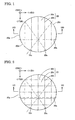
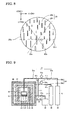
- a further characteristic of the present freestanding III-nitride single-crystal substrate 20 p is that it includes one or more high-dislocation-density regions 20 h , and a plurality of low-dislocation-density regions 20 k where the dislocation density is lower than that of the high-dislocation-density regions 20 h .
- the fact that the present freestanding III-nitride single-crystal substrate 20 p includes the high-dislocation-density regions 20 h and low-dislocation-density regions 20 k makes it possible to arrest the propagation of cracks arising in the substrate, making it possible to prevent fracturing of the substrate.
- the ratio of the dislocation density of the high-dislocation-density region(s) 20 h to the dislocation density of the low-dislocation-density regions 20 k is sufficiently large to check the propagation of cracks in the substrate, and thus the ratio of the dislocation density of the high-dislocation-density region(s) 20 h to the average dislocation density is sufficiently large to check the propagation of cracks in the substrate.
- the dislocation-density distribution in the substrate be non-uniform, to make the ratio of the dislocation density of the high-dislocation-density region(s) 20 h to the average dislocation density sufficiently large, the propagation of cracks arising in the substrate can be arrested, enabling fracturing of the substrate to be prevented.
- the size sufficient to arrest the propagation of cracks will differ depending on the crystalline structure and chemical composition of the substrate.
- freestanding III-nitride single crystal substrates in which the substrate is of the hexagonal crystal system for example, GaN single-crystal freestanding substrates, AlN single-crystal freestanding substrates, InN single-crystal freestanding substrates, Al x Ga 1- x N (0 ⁇ x ⁇ 1) single-crystal freestanding substrates, and In y Ga 1- y N (0 ⁇ y ⁇ 1) single-crystal freestanding substrates-the ratio of the dislocation density of the high-dislocation-density region(s) 20 h to the average dislocation density is preferably 2 or greater, more preferably 5 or greater, still more preferably 10 or greater.
- "Dislocation density of the high-dislocation-density region(s) 20 h herein means the average density of dark spots quantified by the CL method over the major surface of the high-dislocation-density region(s).
- the present freestanding III-nitride single-crystal substrate 20 p is not particularly limited, so long as the average dislocation density is 5 ⁇ 10 5 cm -2 or less and the ratio of the dislocation density of the high-dislocation-density region(s) 20 h to the average dislocation density is sufficiently large to check the propagation of cracks in the substrate, but from the perspective of managing both to prevent fracturing of the substrate and to prevent detriment to the properties of semiconductor devices obtained by forming an at least single-lamina III-nitride semiconductor layer onto the substrate, the dislocation density of the high-dislocation-density region(s) 20 h preferably is between 5 ⁇ 10 5 cm -2 and 3 ⁇ 10 6 cm -2 , more preferably between 5 ⁇ 10 5 cm -2 and 2 ⁇ 10 6 cm -2 , still more preferably between 5 ⁇ 10 5 cm -2 and 1 ⁇ 10 6 cm -2 .
- the dislocation density of the low-dislocation-density regions 20 k is preferably 1 ⁇ 10 5 cm -2 or less, more preferably 1 ⁇ 10 4 cm -2 or less, still more preferably 1 ⁇ 10 3 cm -2 or less.
- Dislocation density of the low-dislocation-density region(s) 20 k herein means the average density of dark spots quantified by the CL method over the major surface of the low-dislocation-density regions 20 k .
- the present freestanding III-nitride single-crystal substrate 20 p have a hexagonal crystal-system structure, and that any chosen ⁇ 1-100 ⁇ plane 20 c in the substrate intersect the one or more high-dislocation-density regions 20 h .
- a freestanding III-nitride single crystal substrate having a hexagonal crystal-system structure has as the cleavage planes, which are most liable to fracture, the ⁇ 1-100 ⁇ planes 20c.
- any chosen ⁇ 1-100 ⁇ plane 20c does not include a ⁇ 1-100 ⁇ plane 20 d that is present only on the peripheral edge of the substrate. It could be that such a ⁇ 1-100 ⁇ plane 20 d does not intersect the high-dislocation-density region(s) 20 h . Nevertheless, even if there is a ⁇ 1-100 ⁇ plane 20 d that is present only on the peripheral edge of the substrate, it will not be a problem, in that it will not lead to the substrate thereby fracturing.
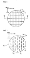
- the one or more high-dislocation-density regions 20 h in the present freestanding III-nitride single-crystal substrate 20 p are patterned in a geometry, seen from the major surface of the substrate, that preferably includes any of striped patterns (cf. Fig. 1 ), polygonally checkered patterns (cf. Fig. 2 ), periodically arrayed islet patterns (cf. Fig. 7 ), or nonrepetitive patterns (cf. Fig. 8 ). That the one or more high-dislocation-density regions 20 h are patterned in a geometry, seen from the major surface of the substrate, that includes any of striped patterns (cf. Fig.
- the polygonally checkered pattern is a square-check pattern
- the polygonal form constituting the polygonally checkered pattern may be, other than square, triangular, rectangular, rhomboid, parallelogrammic, trapezoidal, hexagonal, etc.
- the high-dislocation-density regions 20 h to be geometries whereby any chosen ⁇ 1-100 ⁇ plane 20c intersects the one or more high-dislocation-density regions 20 h ; the high-dislocation-density regions 20 h do not have to be continuous, and the positional relationships between each high-dislocation-density region 20 h separate from another are not limited to the positional relationships depicted in Fig. 7 or Fig. 8 .
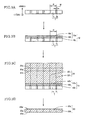
- the first manufacturing method includes: a step ( Fig. 3A and Fig. 4 ) of preparing a starting substrate 1 constituted by III-nitride crystal having matrices 1 s , and inversion domains 1 t in which the polarity in the ⁇ 0001> directions is inverted with respect to that of the matrices 1 s ; a step ( Fig. 3B ) of growing III-nitride crystal 10 by liquid-phase deposition onto the matrices 1 s and inversion domains 1 t in the starting substrate 1; a step ( Fig.
- Fig. 3C is an outline section diagram along IIIA-IIIA in Fig. 4
- Fig. 3D is an outline section diagram along IIID-IIID in Fig. 1 .
- such a starting substrate 1 is manufactured by a facet-growth method based on hydride vapor-phase epitaxy (HVPE)-for example, as described in paragraphs [0221] through [0271] of Japanese Unexamined Pat. App. Pub. No. 2003-183100 .
- HVPE hydride vapor-phase epitaxy
- the dislocation density of the matrices 1 s of the starting substrate 1 will be low, while the dislocation density of the inversion domains 1 t in the starting substrate 1 will, compared with that of the matrices 1 s , be high.
- first zones 10 s of the III-nitride crystal 10 grown onto the matrices 1 s of the starting substrate 1 grow as crystal inheriting the polarity and low-density dislocations of the matrices 1 s .
- second zones 10 t of the III-nitride crystal 10 grown onto the inversion domains 1 t in the starting substrate 1 grow as crystal inheriting the polarity and high-density dislocations of the inversion domains 1 t .
- the liquid-phase deposition method is not particularly limited, but from the perspective of epitaxially growing III-nitride crystal whose dislocation density is low, Na flux growth is preferred.
- the crystal growth rate in the first zones 10 s is greater than the crystal growth rate in the second zones 10 t . Therefore, as the III-nitride crystal 10 grows, the first zones 10 s cover and bury over the second zones 10 t . In this way growing the III-nitride crystal 10 leaves only the first zones 10 s present at and over a certain crystal thickness, whereby at least the surface has a singular polarity.
- low-dislocation-density regions 10 k where the crystal grows onto the matrices 1 s of the starting substrate 1
- high-dislocation-density regions 10 h where the crystal grows onto the buried second zones 10 t are included.
- high-dislocation-density regions 10 h will not be contained in the first zones 10 s .
- the pitch P of the inversion domains 1 t of the starting substrate 1 be 0.1 to 30 mm, and the width W thereof be 0.01 to 0.1 mm.
- the pitch P of the inversion domains 1 t of the starting substrate 1 be 0.01 to 0.1 mm, and the width W thereof be 0.0001 to 0.01 mm.
- the III-nitride single crystal 20 grown onto the III-nitride crystal 10 includes low-dislocation-density regions 20 k where the crystal grows onto the low-dislocation-density regions 10 k in the first zones 10 s of the III-nitride crystal 10, inheriting the zones' low-density dislocations, and high-dislocation-density regions 20 h where the crystal grows onto the high-dislocation-density regions 10 h in the first zones 10 s of the III-nitride crystal 10, inheriting the zones' high-density dislocations.
- the vapor-phase deposition method is not particularly limited, but from the perspective of epitaxially growing crystal of high dislocation density at an advanced rate, HVPE (hydride vapor-phase epitaxy) is preferred.
- the III-nitride single crystal 20 grown by vapor-phase deposition is sliced along planes 20 u and 20 v parallel to the major surface of the starting substrate 1, after which the cut sides are polished to yield a freestanding III-nitride single crystal substrate 20 p having major surfaces 20 m and 20 n .
- the substrate thickness is preferably 100 ⁇ m or greater, more preferably 200 ⁇ m or greater, still more preferably 300 ⁇ m or greater.
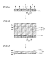
- the second manufacturing method includes: a step ( Figs. 5A and 6 ) of arranging a plurality of III-nitride crystal chip substrates 11 a and 11 b so that their major surfaces parallel each other, and so that their lateral sides adjoin each other, to form a III-nitride crystal aggregate substrate 11; a step ( Fig. 5B ) of growing III-nitride single crystal 20 by vapor-phase deposition onto the major surface of the III-nitride crystal aggregate substrate 11; and a step ( Figs. 5B and 5C ) of processing the III-nitride single crystal 20 to form a freestanding III-nitride single crystal substrate 20 p .
- Fig. 5A is an outline section diagram along VA-VA in Fig. 6
- Fig. 5C is an outline section diagram along VC-VC in Fig. 2 .
- the geometry of the major surfaces of the III-nitride crystal chip substrates 11 a and 11 b utilized in the step of forming the III-nitride crystal aggregate substrate 11 is not particularly limited, but from the viewpoint of tiling over, without gaps, any given planar surface, a triangular, quadrangular or hexagonal geometry is preferable, while an equilateral-triangular, square, rectangular, rhomboid, parallelogrammic, trapezoidal or regular-hexagonal geometry is more preferable.
- the plane orientations of the major surfaces of the plurality of III-nitride crystal chip substrates 11 a and 11 b be, from the standpoint of growing III-nitride single crystal 20 of superior crystallinity, identical or almost identical.
- the plane orientations of the major surfaces of the plural III-nitride crystal chip substrates 11 a and 11 b preferably are minutely displaced from each other.
- the direction of the plane-orientation displacement may be along a tilt line (direction slanted with respect to the c -axis of the III-nitride crystal) or may be along a twist line (direction skewed around the c -axis of the III-nitride crystal).
- the III-nitride crystal chip substrates 11 a and 11 b are more preferably arranged so that the directions of the plane-orientation displacement of the major surfaces of the adjoining III-nitride crystal chip substrates 11 a and 11 b will be such that the displacements cancel each other out.
- the directions of the plane-orientation displacement of the major surfaces of the adjoining III-nitride crystal chip substrates 11 a and 11 b will be such that the displacements cancel each other out.
- III-nitride crystal chip substrate 11 a with major surface having plane orientation in direction A III-nitride crystal chip substrate 11 b with major surface having plane orientation in direction B are disposed with the directions of the plane-orientation displacement of the major surfaces of the adjoining III-nitride crystal chip substrates 11 a and 11 b being such that the displacements cancel each other out.
- the III-nitride single crystal 20 grown onto the III-nitride crystal aggregate substrate 11 includes low-dislocation-density regions 20 k where the crystal grows onto the respective major surfaces of the III-nitride crystal chip substrates 11 a and 11 b of the III-nitride crystal aggregate substrate 11, and high-dislocation-density regions 20 h where the crystal grows over the contiguity plane 11 e between the III-nitride crystal chip substrates 11 a and 11 b where they adjoin each other.
- the vapor-phase deposition method is not particularly limited, but from the perspective of epitaxially growing crystal of high dislocation density at an advanced rate, HVPE (hydride vapor-phase epitaxy) is preferred.
- the III-nitride single crystal 20 grown by vapor-phase deposition is sliced along planes 20 u and 20 v parallel to the major surface of the III-nitride crystal aggregate substrate 11, after which the cut sides are polished to yield a freestanding III-nitride single crystal substrate 20 p having major surfaces 20m and 20 n .
- the substrate thickness is preferably 100 ⁇ m or greater, more preferably 200 ⁇ m or greater, still more preferably 300 ⁇ m or greater.
- a semiconductor device 90 manufacturing method that is another mode of embodying the present invention is a method of manufacturing a semiconductor device 90 utilizing a freestanding III-nitride single crystal substrate 20 p of Embodying Mode 1, and specifically is provided with a step of utilizing the freestanding III-nitride single crystal substrate 20 p to prepare a semiconductor device substrate 90 p , and step of forming an at least single-lamina III-nitride semiconductor layer 70 onto the semiconductor device substrate 90 p .
- the semiconductor device substrate 90 p prepared utilizing the freestanding III-nitride single crystal substrate 20 p comprises III-nitride single crystal 20 in which the average dislocation density is not greater than 5 ⁇ 10 5 cm -2 , including one or more high-dislocation-density regions 20 h and a plurality of low-dislocation-density regions 20 k in which the dislocation density is lower than that of the high-dislocation-density region(s) 20 h .
- Manufacture therefore without giving rise to fractures in the semiconductor device substrate 90 p enables the production at high yield rates of semiconductor devices with superior device properties.
- the method of preparing the semiconductor device substrate 90 p is not particularly limited as long as the substrate that is prepared comprises III-nitride single crystal 20, having one major surface 90 m , of average dislocation density not greater than 5 ⁇ 10 5 cm -2 and including one or more high-dislocation-density regions 20 h and a plurality of low-dislocation-density regions 20 k in which the dislocation density is lower than that of the high-dislocation-density region(s) 20 h , the following method is given as an example.
- a freestanding III-nitride single crystal substrate 20 p of Embodying Mode 1 may be prepared. While the method of preparing the freestanding III-nitride single crystal substrate 20 p of Embodying Mode 1 is not particularly limited, the First Manufacturing Method or the Second Manufacturing Method in the freestanding III-nitride single crystal substrate manufacturing methods of Embodying Mode 1 can be utilized.
- a template substrate may be prepared in which are bonded a III-nitride single crystal 20 q that is the product of thinning down to a film a freestanding III-nitride single crystal substrate 20 p , and a heterosubstrate 90 pb whose chemical composition differs from that of the III-nitride single crystal 20.
- the afore-described template substrate can be prepared in the following way.
- a freestanding III-nitride single crystal substrate 20 p referring to Fig. 12A , is prepared.
- the heterosubstrate 90 pb is bonded to the major surface of the freestanding III-nitride single crystal substrate 20 p .
- the heterosubstrate 90 pb is not particularly limited as long as it is a material capable of bonding with the freestanding III-nitride single crystal substrate 20 p , and substrates having durability suited to the manufacture of the target semiconductor devices can be selected.
- III-nitride substrates whose chemical composition differs from that of the III-nitride single crystal 20; sapphire substrates; SiC substrates; Si substrates; ZnSe substrates; ZnO substrates; ZnS substrates; MgO substrates; quartz substrates; carbon substrates; diamond substrates; Ga 2 O 3 substrates; and ZrB substrates.
- the method of bonding the heterosubstrate 90 pb is not particularly limited, from the perspective of enabling uniform bonding at low temperatures, methods such as surface-activated bonding and fusion bonding are preferable.
- surface-activated bonding means a technique whereby the surfaces to be bonded are bombarded with a plasma to superficially active them, and then the surfaces are joined together
- fusion bonding means a technique of applying pressure and heat to cleaned mating surfaces to be bonded, and joining the surfaces together.
- the freestanding III-nitride single crystal substrate 20 p is divided along a plane that is a predetermined distance T (for example, between 0.01 ⁇ m and 100 ⁇ m) from the single-crystal substrate's interface with the heterosubstrate 90 pb .
- the method of dividing the freestanding III-nitride single crystal substrate 20 p is not particularly limited, and methods employing devices such as electric-discharge machines, wire saws, dicing saws, internal diameter saws, and laser saws can be cited.
- ions into a region of the freestanding III-nitride single crystal substrate that is alongside the surface that bonds the heterosubstrate and which has a predetermined depth T from that surface, thereafter bond on the heterosubstrate, and, by means of heat, force, etc., apply stress to the single-crystal substrate to divide it along the ion-implanted region.
- hydrogen ions, helium ions, etc. are employed as the implantation ions.
- a template substrate including the heterosubstrate 90 pb and, formed onto the heterosubstrate 90 pb as a III-nitride seed crystal layer 90 pa , the III-nitride single crystal layer 20 q of thickness T is obtained.
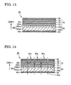
- a one major surface 90 m of the semiconductor device substrate 90 p Onto a one major surface 90 m of the semiconductor device substrate 90 p , an n + -type GaN layer 72, an n -type GaN layer 74, and a p -type GaN layer 76, for example, are formed as an at least single-lamina III-nitride semiconductor layer 70. In this way a p - n junction plane 90 j is formed in between the p -type GaN layer 76 and the n -type GaN layer 74.
- the one major surface 90 m corresponds in the semiconductor device substrate 90 p to the freestanding III-nitride single crystal substrate 20 p (cf. Fig.
- the method of forming the at least single-lamina III-nitride semiconductor layer 70 is not particularly limited, from the perspective of epitaxially growing low-dislocation-density, superior-crystallinity semiconductor layers, vapor deposition methods such as metalorganic chemical vapor deposition (MOCVD), hydride vapor-phase epitaxy (HVPE), molecular-beam epitaxy (MBE), and sublimation growth are preferably utilized.
- MOCVD metalorganic chemical vapor deposition
- HVPE hydride vapor-phase epitaxy
- MBE molecular-beam epitaxy
- an Ni/Au laminate electrode is formed, as a p -side electrode 82, onto the p -type GaN layer 76 (with the Ni layer in contact with the p -type GaN layer), and a Ti/Al laminate electrode is formed, as an n -side electrode 84, onto the other major surface 90n of the semiconductor device substrate 90 p (with the Ti layer in contact with the semiconductor device substrate 90 p ), yielding a semiconductor device 90.
- the method of forming the p -side electrode 82 and n -side electrode 84 is not particularly limited, from a high productivity standpoint, such methods as evaporation deposition and sputter deposition are preferable.
- the p -side electrode 82, p -type GaN layer 76, and a portion of the n -type GaN layer 74 are mesa-etched along dicing streets 90 d in the just-described semiconductor device 90. Subsequently, by segmenting the semiconductor device 90 along the dicing streets 90 d , semiconductor device chips 90 c are obtained. By segmenting a single semiconductor device 90 into ten chips C1 through C10, for example, ten semiconductor device chips 90 c are produced.
- freestanding GaN single crystal substrates (freestanding III-nitride single crystal substrates) were produced in the following manner, according to the above-described First Manufacturing Method.
- Fig. 3A and Fig. 4 2-inch (5.08 cm) diameter, 350- ⁇ m thick starting substrates 1 of GaN crystal (termed GaN starting substrates 1 hereinafter) were prepared, having a plurality of matrices 1 s in which the dislocation density was 0.1 to 1 ⁇ 10 5 cm -2 , and a plurality of inversion domains 1 t in which the dislocation density was 0.1 to 1 ⁇ 10 9 cm -2 .
- the (0001) surface (Ga-atom surface) of the matrices 1 s appeared, while the (000-1) surface (N-atom surface) of the inversion domains 1 t appeared.
- the inversion domains 1 t extended from one edge to the other edge of the starting substrates 1, along their ⁇ 1-100> directions in a striped formation.
- sample GaN starting substrates 1 of two kinds were prepared: Starting Substrates A, in which the pitch P of the inversion domains 1 t was 1 mm and the width W thereof was 0.01 mm; and Starting Substrates B, in which the pitch of the inversion domains 1 t was 0.05 mm and the width was 0.01 mm.
- GaN crystal III-nitride crystal 10
- GaN crystal was grown in the following manner by the Na flux method onto the two types of GaN starting substrate 1 just described-Starting Substrates A and Starting Substrates B.
- a crystal-growth reactor employed in growing the III-nitride crystal by the Na-flux method is furnished with, for example: an outer chamber 39; a thermally insulating component 37 disposed in the inside of the outer chamber 39; a heater 35 disposed in the inside of the insulating component 37; and an inner chamber 31 disposed inward of the heater 35.
- a crystal-growth vessel 33 for growing within it the III-nitride crystal 10 is disposed inside the inner chamber 31. Further, the opening in the crystal-growth vessel 33 may be covered by a lid 34.
- the material of the crystal-growth vessel 33 and the lid 34 is not particularly limited as long as it does not react with solvent 3 and nitrogen-containing gas 5, and is of high mechanical strength and heat resistance, a material such as BN (boron nitride) is preferable.
- the material of the inner chamber 31 is not particularly limited as long as it is of high mechanical strength and heat resistance, materials such as stainless and heat-resistant steels are preferable.
- the material of the outer chamber 39 is not particularly limited as long as it is of high mechanical strength and heat resistance, materials such as stainless steels are preferable.
- the material of the thermally insulating component 37 is not particularly limited as long as it is of high mechanical strength, heat resistance, and insulating ability, materials such as graphite wool are preferable.
- the present crystal-growth reactor is also provided with: a nitrogen-containing-gas supply device 41 connected to the inner chamber 31 by a first supply line 51; a pressurizing gas supply device 43 connected to the outer chamber 39 by a second supply line 53; and a evacuation pump 45 connected to the outer chamber 39 by a third supply line 55.
- the first supply line 51 herein is furnished with a valve 51v for adjusting the supply flow volume of the nitrogen-containing gas 5, while the supply-line section 51a to the inner chamber 31 side of the valve 51v is provided with a first pressure gauge 51p.
- the second supply line 53 is furnished with a valve 53v for adjusting the supply flow volume of the pressurizing gas 7, while the supply-line section 53a to the outer chamber 39 side of the valve 53v is provided with a second pressure gauge 53p.
- the third supply line 55 is furnished with a valve 55v for adjusting the exhaust flow volume.
- the growth reactor is additionally provided with a fourth supply line 57 connecting the section 51 a of the first supply line 51 to the inner chamber 31 side of valve 51 v with the section 55 a of the third supply line 55 to the outer chamber 39 side of valve 55 v .
- the fourth supply line 57 is provided with a valve 57 v .
- the section 51 b of the first supply line 51 to the nitrogen-containing-gas supply device 41 side of valve 51 v the section 53 b of the second supply line 53 to the pressurizing-gas supplying device 43 side of valve 53 v
- the section 55 b of the third supply line 55 to the evacuation-pump 45 side of valve 55 v are also illustrated.
- the above-described GaN starting substrate 1 of the two types were each placed on the bottom of a boron-nitride crucible (crystal-growth vessel 33) of 60 mm inner diameter and 20 mm depth, with the aforementioned one major surface facing up (substrate placement substep).
- a boron-nitride crucible crystal-growth vessel 33
- metallic Ga 99.9999 mol% purity
- metallic Na solvent 3
- the metallic Ga and metallic Na (solvent 3), which are solid at room temperature (approximately 25°C), by subsequent heating were liquefied into a metallic Ga-Na melt in which the molar ratio of metallic Ga (Group-III metal M III ) to metallic Na (alkali metal M A ) M III : M A 31 : 69, with the depth from the surface of the metallic Ga-Na melt (solvent 3) to the major surface of the GaN starting substrates 1 being 5 mm.
- the BN crucible (crystal-growth vessel 33) in which the GaN starting substrates, as well as the metallic Ga and metallic Na (solvent 3), had been contained was set inside the inner chamber 31.
- a boron-nitride lid 34 was placed on top of the BN crucible (crystal-growth vessel 33)-(crystal-growth container placement substep).
- a vacuum pump (the evacuation pump 45) was employed to evacuate the interior of the inner chamber 31 and outer chamber 39 (evacuation substep).
- the vacuum level in the inner chamber 31 and outer chamber 39 following evacuation was 1 ⁇ 10 -3 Pa.
- Nitrogen-containing gas 5 and pressurizing gas 7 were then respectively supplied into interior of the inner chamber 31 and outer chamber 39 so that the internal pressure of each chamber would be 1 MPa (nitrogen-containing gas supply substep).
- a high-purity nitrogen gas of 99.99999 mol% purity was used for the nitrogen-containing gas 5 supplied inside the inner chamber 31.
- nitrogen gas of 99.9999 mol% purity was used for the pressurizing gas 7 supplied to the outer chamber 39.
- the heater 35 which was of the resistive heating type, was employed to heat the inside of the inner chamber 31 and outer chamber 39, and bring the temperature of the inner chamber 31 interior overall to 870°C (heating substep).
- This heating liquefied the metallic Ga and metallic Na (solvent 3) placed in the inner chamber 31, covering the aforementioned major surface of the GaN starting substrates 1 and dissolving the high-purity nitrogen gas (nitrogen-containing gas 5) into the liquefied metallic Ga and metallic Na, i.e., the Ga-Na melt (solvent 3).
- the amount of the nitrogen-containing gas 5 supplied, and the amount of heat added, to the inner chamber 31 were adjusted to bring the internal pressure of the inner chamber 31 to 3 MPa (crystal-growth pressure) with the temperature of the inner chamber 31 interior overall being kept at 870°C (crystal-growth temperature), and GaN crystal (III nitride crystal 10) was grown onto the said major surface of the GaN starting substrates 1 for 200 hours (crystal-growth substep).
- the amount of the nitrogen gas (pressurizing gas 7) supplied to the outer chamber 39 was adjusted to make the internal pressure of the outer chamber 39 in the range of from 0.01 MPa to 0.1 MPa less than that of the internal pressure of the inner chamber 31. That is, likewise as during heating, during crystal growth the pressure situation was made so that 0.01 MPa ⁇ ⁇ (inner-chamber internal pressure) - (outer-chamber internal pressure) ⁇ ⁇ 0.1 MPa.
- the interiors of both the inner chamber 31 and the outer chamber 39 were cooled and depressurized, with the relationship 0.01 MPa ⁇ ⁇ ( inner-chamber internal pressure) - (outer-chamber internal pressure) ⁇ ⁇ 0.1 MPa being maintained, and from the Ga-Na melt (solvent 3) in the BN crucible (crystal-growth vessel 33) within the inner chamber 31 having been cooled to 30°C, the GaN crystal (III nitride crystal 10) grown onto the GaN starting substrates 1 was taken out with tweezers. The thickness of the obtained GaN crystal was 200 ⁇ m. That meant that the GaN crystal-growth rate was 1 ⁇ m/hr.
- GaN crystal A (III-nitride crystal 10) produced on Starting Substrates A (starting substrates 1) contained low-dislocation-density regions 10 k , grown onto the matrices 1 s in the Starting Substrates A, and high-dislocation-density regions 10 h , grown onto the buried second zones 10 t , and had an average dislocation density of 5 ⁇ 10 5 cm -2 , with the dislocation density of the low-dislocation-density regions being 2 to 10 ⁇ 10 4 cm -2 and the dislocation density of the high-dislocation-density regions being 1 to 2 ⁇ 10 6 cm -2 .
- GaN crystal B III-nitride crystal 10
- Starting Substrates B starting substrates 1
- GaN crystal B III-nitride crystal 10
- Starting Substrates B starting substrates 1
- a substrate's dislocation-density profile being "essentially uniform" means that in that substrate, the ratio of the dislocation density of the high-dislocation-density regions to the average dislocation density is less than 2, for example.
- the dislocation density (dark-spot density under CL) of the substrates was calculated by determining the number of dark spots per unit area (surface area of a 100 ⁇ m ⁇ 100 ⁇ m square region) where the substrate major surface was measured by CL, in 500 locations on points of a 100- ⁇ m pitch grid where the major surface intersected the high-dislocation-density regions perpendicular to their longitudinal direction.
- III-nitride single crystal 20 was grown in the following manner by HVPE onto the aforedescribed two types of GaN crystal (III-nitride crystal 10).
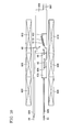
- a crystal holder 602 for retaining the GaN crystal (III-nitride crystal 10) is disposed inside a reaction chamber 601; and a Group III chloride gas synthesis chamber 603 for synthesizing Group III chloride gas 63 that is introduced into the reaction chamber 601, an HCl gas introduction line 605 for introducing HCl gas 61 into the III-chloride gas synthesis chamber 603, a nitrogen precursor gas introduction line 606 for introducing nitrogen precursor gas 66 into the reaction chamber 601, and an exhaust duct 607 for exhausting the post-reaction gases are installed in the reactor.
- a Group III metal boat 604 into which Group IIII metal 62 is stored is disposed in the III-chloride gas synthesis chamber 603.
- heaters 608, 609 and 610 are installed surrounding the III-chloride gas synthesis chamber 603 and the reaction chamber 601, for heating both the Group III metal boat 604 and the GaN crystal (III-nitride crystal 10).
- the Ga chloride gas (Group III chloride gas 63) that is introduced into the reaction chamber 601 is synthesized to begin with.
- the Ga boat (Group III metal boat 604) disposed inside the Ga chloride synthesis chamber (III-chloride gas synthesis chamber 603) is heated with heater 609 to 800°C, HCl gas is introduced inside the Ga chloride synthesis chamber (III-chloride gas synthesis chamber 603) via the HCl gas introduction line 605, and the HCl gas 61 and the Ga (III-nitride metal 62) inside the Ga boat (Group III metal boat 604) are reacted to synthesize Ga chloride gas (Group III chloride gas 63).
- the HCl gas 61 in this case is introduced into the Ga chloride synthesis chamber (III-chloride gas synthesis chamber 603) together with a carrier gas such as H 2 .
- Ga chloride gas (Group III chloride gas 63) just described and NH 3 gas (nitrogen precursor gas 66) were introduced into the reaction chamber 601 together with the H 2 gas as a carrier gas, and the Ga chloride gas (Group III chloride gas 63) and NH 3 gas (nitrogen precursor gas 66) were reacted over the GaN crystal (III-nitride crystal 10), placed atop the crystal holder 602 inside the reaction chamber 601 and heated to 1100°C, whereby for 50 hours single-crystal GaN was grown, yielding a 10-mm thick GaN single-crystal.
- the GaN crystal (III-nitride crystal 10) was disposed atop the crystal holder 602, slanted 10° with respect to the horizontal, and rotated at a turning rate of 60 rpm. Also, the partial pressure of the Ga chloride gas (Group III chloride gas 63) was made 5.065 kPa (0.05 atm), and the partial pressure of the NH 3 gas (nitrogen precursor gas 66), 10.13 kPa (0.1 atm).
- GaN single crystal A (III-nitride single crystal 20) produced on GaN crystal A (III-nitride crystal 10) contained low-dislocation-density regions 20 k , grown onto the matrices 1 s in the GaN starting substrates A , and high-dislocation-density regions 20 h , grown onto the buried second zones 10 t , and had an average dislocation density of 3 ⁇ 10 5 cm -2 , with the dislocation density of the low-dislocation-density regions being 2 to 10 ⁇ 10 4 cm -2 and the dislocation density of the high-dislocation-density regions being 5 to 10 ⁇ 10 5 cm -2 .
- GaN single crystal B (III-nitride single crystal 20) produced on GaN crystal B (III-nitride crystal 10)-which was produced on GaN starting substrates B -formed essentially with low-dislocation-density regions 20 k only, grown onto the matrices 1 s in the GaN crystal B (III-nitride crystal 10), and had an average dislocation density of 3 ⁇ 10 5 cm -2 , with an essentially uniform dislocation-density profile, in that the dislocation density of the low-dislocation-density regions was within a 2.5 to 3.8 ⁇ 10 5 cm -2 range.
- the GaN single crystal (III-nitride single crystal 20) obtained in the manner described above was sliced along planes 20 u and 20 v parallel to the major surface of the starting substrate 1, yielding freestanding GaN single crystal wafers (freestanding III-nitride single crystal wafers) of 500 ⁇ m thickness. Subsequently, chemical-mechanical polishing (CMP) was employed to process the major surface of the freestanding GaN single crystal wafers (freestanding III-nitride single crystal wafers) to a specular finish, yielding a plurality of 400- ⁇ m thick freestanding GaN single crystal substrates (freestanding III-nitride single crystal substrates 20 p ).
- CMP chemical-mechanical polishing
- the plurality of freestanding GaN single crystal substrates just described was grouped into: ten substrates (Group 1) whose average dislocation density was in the range of 3 to 5 ⁇ 10 5 cm -2 , dislocation density of the low-dislocation-density regions, 2 to 10 ⁇ 10 4 cm -2 , and dislocation density of the high-dislocation-density regions, 10 to 20 ⁇ 10 5 cm -2 ; ten substrates (Group 2) whose average dislocation density was 3 to 5 ⁇ 10 5 cm -2 , and having an essentially uniform dislocation-density profile (the ratio of dislocation density of the high-dislocation-density regions to the average dislocation density was less than 2); and ten substrates (Group 3) whose average dislocation density was 10 to 20 ⁇ 10 5 cm -2 , and having an essentially uniform dislocation-density profile.
- the Group 1 substrates were taken as Embodiment I of the invention in the present application, while the Group 2 and Group 3 substrates were taken as Compar
- the ten freestanding GaN single crystal substrates of each group were each housed individually in a wafer tray of polypropylene for a single 2-inch wafer, and fixed with a spring. For each group of the manufactured substrates that had been housed in this way, the ten wafer trays were dropped in a freefall onto a concrete floor from a height of 50 cm. With the Group 1 substrates, among the ten there were none that fractured (Embodiments 1-1 through 1-10). With the Group 2 substrates, among the ten there were seven that fractured (Comparative Examples II-1 through II-10). With the Group 3 substrates, among the ten there were 2 that fractured (Comparative Examples III-1 through III-10). The results are tabulated in Tables I through III.
- Comparative Example III evidences that among the freestanding III-nitride single crystal substrates in which the dislocation-density profile is essentially uniform, compared with substrates in which the average dislocation density is a large 10 to 20 ⁇ 10 5 cm -2 , substrates in which the average dislocation density is a small 3 to 5 ⁇ 10 5 cm -2 are fracture-prone.
- freestanding GaN single-crystal substrate I-10 (freestanding III-nitride single crystal substrate 20 p ) obtained in Embodiment I-10 was prepared as a semiconductor device substrate 90 p .
- a one major surface 90 m corresponds to the major surface 20 m of the freestanding III-nitride single crystal substrate 20 p ) of the freestanding GaN single-crystal substrate I-10 (semiconductor device substrate 90 p ), by MOCVD a 0.6- ⁇ m thick n + -type GaN layer 72, a 7- ⁇ m thick n -type GaN layer 74 (electron density of 3 ⁇ 10 16 cm -3 ), and a 0.5- ⁇ m thick p -type GaN layer 76 (Mg atom density of 7 ⁇ 10 17 cm -3 ) were grown, in that order, as an at least single-lamina III-nitride semiconductor layer 70.
- a p-n junction plane 90 j was formed in between the p -type GaN layer 76 and the n -type GaN layer 74.
- an Ni layer and an Au layer were formed in that order as a p -side electrode 82, by evaporation deposition onto the p -type GaN layer 76 to create an Ni/Au laminate electrode.
- a Ti layer and an Al layer were formed in that order as an n -side electrode 84 by evaporation deposition onto the other major surface 90n (referring to Fig.
- the major surface 90 n corresponds to the major surface 20n of the freestanding III-nitride single crystal substrate 20 p ) of the freestanding GaN single-crystal substrate I-10 (semiconductor device substrate 90 p ), creating a Ti/Al laminate electrode. In this way a semiconductor device 90 was produced.
- the aforedescribed semiconductor device 90-the p -side electrode 82, p -type GaN layer 76, and a portion of the n -type GaN layer 74- was mesa-etched along its dicing streets 90d. Subsequently, by segmenting the semiconductor device 90 along the dicing streets 90 d into ten chips C1 through C10 whose p - n junction plane 90 j size was 1 cm ⁇ 1 cm, with no fractures arising in the semiconductor device 90, ten semiconductor device chips 90c in which the p-n junction plane 90 j surface area was 1 cm 2 were obtained from the semiconductor device 90.
- a reverse breakdown voltage test was conducted on the ten semiconductor device chips obtained, whereupon all ten semiconductor device chips had a reverse breakdown voltage of not less than 500 V, thus exhibiting exceedingly superior reverse breakdown voltage characteristics.
- a plurality of high-dislocation-density region 20 h were present in the freestanding GaN single-crystal substrate I-10 (freestanding III-nitride single crystal substrate 20 p ) utilized as the semiconductor device substrate 90 p for the semiconductor device chips 90 c , extending along ⁇ 1-100> directions in the substrate I-10, at a pitch of 1 mm along ⁇ 11-20> directions in the substrate I-10.
- the semiconductor device substrates 90 p in all of the semiconductor device chips 90 c contained a plurality of high-dislocation-density regions 20 h and low-dislocation-density regions 20 k . Accordingly, by utilizing a freestanding III-nitride single-crystal substrate in which the average dislocation density is not greater than 5 ⁇ 10 5 cm -2 , and that includes one or more high-dislocation-density regions, and a plurality of low-dislocation-density regions in which the dislocation density is lower than that of the high-dislocation-density regions, semiconductor devices with enhanced device characteristics were obtained at high yields.
- a freestanding III-nitride single crystal substrate involving the present invention is utilized in applications including light-emitting devices such as light-emitting diodes and laser diodes, in electronic devices such as rectifiers, bipolar transistors, field-effect transistors, and high electron mobility transistors (HEMTs), semiconductor sensors such as temperature sensors, pressure sensors, radiation sensors, or visible-blind ultraviolet detectors, surface acoustic wave devices (SAW devices), vibrators, resonators, oscillators, microelectromechanical system (MEMS) parts, and piezoelectric actuators.
- light-emitting devices such as light-emitting diodes and laser diodes
- electronic devices such as rectifiers, bipolar transistors, field-effect transistors, and high electron mobility transistors (HEMTs)
- semiconductor sensors such as temperature sensors, pressure sensors, radiation sensors, or visible-blind ultraviolet detectors
- SAW devices surface acoustic wave devices
- vibrators vibrators
- resonators oscillators
- MEMS microelect
Landscapes
- Chemical & Material Sciences (AREA)
- Engineering & Computer Science (AREA)
- Crystallography & Structural Chemistry (AREA)
- Materials Engineering (AREA)
- Metallurgy (AREA)
- Organic Chemistry (AREA)
- Chemical Kinetics & Catalysis (AREA)
- General Chemical & Material Sciences (AREA)
- Inorganic Chemistry (AREA)
- Crystals, And After-Treatments Of Crystals (AREA)
- Led Devices (AREA)
Applications Claiming Priority (2)
| Application Number | Priority Date | Filing Date | Title |
|---|---|---|---|
| JP2008115013 | 2008-04-25 | ||
| JP2008326384A JP2009280482A (ja) | 2008-04-25 | 2008-12-22 | Iii族窒化物単結晶自立基板およびそれを用いた半導体デバイスの製造方法 |
Publications (3)
| Publication Number | Publication Date |
|---|---|
| EP2116636A2 true EP2116636A2 (de) | 2009-11-11 |
| EP2116636A3 EP2116636A3 (de) | 2011-12-07 |
| EP2116636B1 EP2116636B1 (de) | 2020-06-10 |
Family
ID=40984802
Family Applications (1)
| Application Number | Title | Priority Date | Filing Date |
|---|---|---|---|
| EP09005378.6A Active EP2116636B1 (de) | 2008-04-25 | 2009-04-15 | Freistehendes Gruppe-III-Nitrid-Einkristallsubstrat und Verfahren zur Herstellung eines Halbleiterbauelements, das das Substrat einsetzt |
Country Status (5)
| Country | Link |
|---|---|
| US (2) | US20090267190A1 (de) |
| EP (1) | EP2116636B1 (de) |
| JP (1) | JP2009280482A (de) |
| CA (1) | CA2663779A1 (de) |
| TW (1) | TWI548787B (de) |
Cited By (3)
| Publication number | Priority date | Publication date | Assignee | Title |
|---|---|---|---|---|
| US20130072005A1 (en) * | 2011-09-15 | 2013-03-21 | Hitachi Cable, Ltd | Method for manufacturing nitride semiconductor substrate |
| EP2602362A4 (de) * | 2010-08-03 | 2015-05-06 | Sumitomo Electric Industries | Verfahren zur züchtung von gruppe-iii-nitrid-kristallen |
| EP3103899A4 (de) * | 2014-03-03 | 2018-01-03 | Osaka University | Verfahren zur herstellung eines gruppe-iii-nitridkristalls, gruppe-iii-nitridkristall, halbleiterbauelement und vorrichtung zur herstellung des gruppe-iii-nitrid-kristalls |
Families Citing this family (12)
| Publication number | Priority date | Publication date | Assignee | Title |
|---|---|---|---|---|
| JP4259591B2 (ja) * | 2007-01-16 | 2009-04-30 | 住友電気工業株式会社 | Iii族窒化物結晶の製造方法、iii族窒化物結晶基板およびiii族窒化物半導体デバイス |
| EP2559791A4 (de) | 2010-04-13 | 2015-06-10 | Namiki Precision Jewel Co Ltd | Einzelkristallsubstrat, einzelkristallsubstrat mit einem kristallinen film, kristalliner film, verfahren zur herstellung des einzelkristallsubstrats mit dem kristallinen film, verfahren zur herstellung eines kristallinen substrats und verfahren zur herstellung eines elements |
| WO2013058352A1 (ja) * | 2011-10-21 | 2013-04-25 | 三菱化学株式会社 | Iii族窒化物半導体結晶 |
| JP6232186B2 (ja) * | 2013-01-16 | 2017-11-15 | 住友化学株式会社 | 窒化物半導体ウェハのマーキング方法および識別符号付き窒化物半導体ウェハ |
| EP2955253A4 (de) * | 2013-02-08 | 2016-11-23 | Namiki Precision Jewel Co Ltd | Gan-substrat und verfahren zur herstellung des gan-substrats |
| JP6344987B2 (ja) * | 2014-06-11 | 2018-06-20 | 日本碍子株式会社 | 13族元素窒化物結晶層および機能素子 |
| US10584031B2 (en) * | 2016-03-08 | 2020-03-10 | Sciocs Company Limited | Nitride crystal substrate |
| JP6841191B2 (ja) * | 2016-09-06 | 2021-03-10 | 豊田合成株式会社 | Iii族窒化物半導体の製造方法 |
| US10807524B2 (en) * | 2016-11-18 | 2020-10-20 | Saf-T-Glo Limited | Lighting unit |
| US10322928B2 (en) * | 2016-11-29 | 2019-06-18 | Taiwan Semiconductor Manufacturing Co., Ltd. | Multi-layer sealing film for high seal yield |
| JP6595677B1 (ja) * | 2018-08-29 | 2019-10-23 | 株式会社サイオクス | 窒化物半導体基板の製造方法、窒化物半導体基板および積層構造体 |
| WO2021163230A1 (en) * | 2020-02-11 | 2021-08-19 | Slt Technologies, Inc. | Large area group iii nitride crystals and substrates, methods of making, and methods of use |
Citations (3)
| Publication number | Priority date | Publication date | Assignee | Title |
|---|---|---|---|---|
| JP2003183100A (ja) | 2001-10-09 | 2003-07-03 | Sumitomo Electric Ind Ltd | 単結晶窒化ガリウム基板と単結晶窒化ガリウムの結晶成長方法および単結晶窒化ガリウム基板の製造方法 |
| JP2004193371A (ja) | 2002-12-11 | 2004-07-08 | Nec Corp | Iii族窒化物自立基板およびそれを用いた半導体素子ならびにそれらの製造方法 |
| JP2006052102A (ja) | 2004-08-10 | 2006-02-23 | Hitachi Cable Ltd | Iii−v族窒化物系半導体基板及びその製造方法並びにiii−v族窒化物系半導体 |
Family Cites Families (12)
| Publication number | Priority date | Publication date | Assignee | Title |
|---|---|---|---|---|
| JP4032538B2 (ja) * | 1998-11-26 | 2008-01-16 | ソニー株式会社 | 半導体薄膜および半導体素子の製造方法 |
| JP2008037665A (ja) * | 2006-08-02 | 2008-02-21 | Sumitomo Electric Ind Ltd | 窒化ガリウムの結晶成長方法 |
| JP3864870B2 (ja) | 2001-09-19 | 2007-01-10 | 住友電気工業株式会社 | 単結晶窒化ガリウム基板およびその成長方法並びにその製造方法 |
| US7105865B2 (en) * | 2001-09-19 | 2006-09-12 | Sumitomo Electric Industries, Ltd. | AlxInyGa1−x−yN mixture crystal substrate |
| JP3910041B2 (ja) * | 2001-10-29 | 2007-04-25 | シャープ株式会社 | 窒化物半導体レーザ素子及びこれを備えた半導体光学装置 |
| US7323256B2 (en) * | 2003-11-13 | 2008-01-29 | Cree, Inc. | Large area, uniformly low dislocation density GaN substrate and process for making the same |
| JP4622447B2 (ja) * | 2004-01-23 | 2011-02-02 | 住友電気工業株式会社 | Iii族窒化物結晶基板の製造方法 |
| JP4915128B2 (ja) * | 2005-04-11 | 2012-04-11 | 日亜化学工業株式会社 | 窒化物半導体ウエハ及びその製造方法 |
| KR20060127743A (ko) * | 2005-06-06 | 2006-12-13 | 스미토모덴키고교가부시키가이샤 | 질화물 반도체 기판과 그 제조 방법 |
| JP5024722B2 (ja) * | 2005-06-06 | 2012-09-12 | 住友電気工業株式会社 | 窒化物半導体基板とその製造方法 |
| WO2007125914A1 (ja) * | 2006-04-28 | 2007-11-08 | Sumitomo Electric Industries, Ltd. | 窒化ガリウム結晶を作製する方法および窒化ガリウムウエハ |
| JP4259591B2 (ja) * | 2007-01-16 | 2009-04-30 | 住友電気工業株式会社 | Iii族窒化物結晶の製造方法、iii族窒化物結晶基板およびiii族窒化物半導体デバイス |
-
2008
- 2008-12-22 JP JP2008326384A patent/JP2009280482A/ja active Pending
-
2009
- 2009-04-15 EP EP09005378.6A patent/EP2116636B1/de active Active
- 2009-04-16 TW TW098112694A patent/TWI548787B/zh active
- 2009-04-21 US US12/426,963 patent/US20090267190A1/en not_active Abandoned
- 2009-04-22 CA CA002663779A patent/CA2663779A1/en not_active Abandoned
-
2011
- 2011-01-14 US US13/006,429 patent/US8501592B2/en active Active
Patent Citations (3)
| Publication number | Priority date | Publication date | Assignee | Title |
|---|---|---|---|---|
| JP2003183100A (ja) | 2001-10-09 | 2003-07-03 | Sumitomo Electric Ind Ltd | 単結晶窒化ガリウム基板と単結晶窒化ガリウムの結晶成長方法および単結晶窒化ガリウム基板の製造方法 |
| JP2004193371A (ja) | 2002-12-11 | 2004-07-08 | Nec Corp | Iii族窒化物自立基板およびそれを用いた半導体素子ならびにそれらの製造方法 |
| JP2006052102A (ja) | 2004-08-10 | 2006-02-23 | Hitachi Cable Ltd | Iii−v族窒化物系半導体基板及びその製造方法並びにiii−v族窒化物系半導体 |
Cited By (5)
| Publication number | Priority date | Publication date | Assignee | Title |
|---|---|---|---|---|
| EP2602362A4 (de) * | 2010-08-03 | 2015-05-06 | Sumitomo Electric Industries | Verfahren zur züchtung von gruppe-iii-nitrid-kristallen |
| US20130072005A1 (en) * | 2011-09-15 | 2013-03-21 | Hitachi Cable, Ltd | Method for manufacturing nitride semiconductor substrate |
| US9175417B2 (en) * | 2011-09-15 | 2015-11-03 | Sciocs Company Limited | Method for manufacturing a nitride semiconductor substrate |
| EP3103899A4 (de) * | 2014-03-03 | 2018-01-03 | Osaka University | Verfahren zur herstellung eines gruppe-iii-nitridkristalls, gruppe-iii-nitridkristall, halbleiterbauelement und vorrichtung zur herstellung des gruppe-iii-nitrid-kristalls |
| US10266965B2 (en) | 2014-03-03 | 2019-04-23 | Osaka University | Method for producing group-III nitride crystal, group-III nitride crystal, semiconductor device, and device for producing group-III nitride crystal |
Also Published As
| Publication number | Publication date |
|---|---|
| TW201000695A (en) | 2010-01-01 |
| US8501592B2 (en) | 2013-08-06 |
| EP2116636A3 (de) | 2011-12-07 |
| EP2116636B1 (de) | 2020-06-10 |
| TWI548787B (zh) | 2016-09-11 |
| US20120070962A1 (en) | 2012-03-22 |
| JP2009280482A (ja) | 2009-12-03 |
| US20090267190A1 (en) | 2009-10-29 |
| CA2663779A1 (en) | 2009-10-25 |
Similar Documents
| Publication | Publication Date | Title |
|---|---|---|
| EP2116636B1 (de) | Freistehendes Gruppe-III-Nitrid-Einkristallsubstrat und Verfahren zur Herstellung eines Halbleiterbauelements, das das Substrat einsetzt | |
| CN102137961B (zh) | Iii族氮化物晶体及其制造方法 | |
| JP5885650B2 (ja) | 最初のiii族−窒化物種晶からの熱アンモニア成長による改善された結晶性のiii族−窒化物結晶を生成するための方法 | |
| KR101410534B1 (ko) | Ⅲ족 질화물 결정의 제조 방법 | |
| KR101749781B1 (ko) | 단결정 기판, 이를 이용하여 얻어지는 ⅲ족 질화물 결정 및 ⅲ족 질화물 결정의 제조방법 | |
| EP3103899B1 (de) | Verfahren zur herstellung eines gruppe-iii-nitridkristalls | |
| EP2128309A1 (de) | Verfahren zur Herstellung von III-Nitrid-Kristall, III-Nitrid-Kristall-Substrat und Halbleitervorrichtung | |
| JP6885547B2 (ja) | GaN結晶の製造方法 | |
| KR20100113529A (ko) | Ⅲ족 질화물 결정의 성장 방법 | |
| WO2010140564A1 (ja) | 窒化物半導体結晶およびその製造方法 | |
| JP2011063504A (ja) | 窒化物半導体結晶およびその製造方法 | |
| JP6187576B2 (ja) | Iii族窒化物結晶 | |
| US20130052838A1 (en) | Annealing method to reduce defects of epitaxial films and epitaxial films formed therewith | |
| KR20130141576A (ko) | Ⅲ 족 질화물 반도체 기판 및 그 제조 방법, 그리고 반도체 발광 디바이스 및 그 제조 방법 | |
| CN101565854A (zh) | Ⅲ族氮化物单晶自立式衬底及利用该衬底制造半导体装置的方法 | |
| US11932936B2 (en) | Method for producing a group III compound crystal by hydride vapor phase epitaxy on a seed substrate formed on a group III nitride base substrate | |
| JP5542570B2 (ja) | 単結晶窒化アルミニウムの製造方法 | |
| TW201016905A (en) | Method for manufacturing nitride substrate, and nitride substrate | |
| US7892513B2 (en) | Group III nitride crystal and method of its growth | |
| KR20090113190A (ko) | Iii족 질화물 단결정 자립 기판 및 그것을 사용한 반도체 디바이스의 제조방법 | |
| JP2009029673A (ja) | Iii族窒化物結晶およびその成長方法 |
Legal Events
| Date | Code | Title | Description |
|---|---|---|---|
| PUAI | Public reference made under article 153(3) epc to a published international application that has entered the european phase |
Free format text: ORIGINAL CODE: 0009012 |
|
| AK | Designated contracting states |
Kind code of ref document: A2 Designated state(s): AT BE BG CH CY CZ DE DK EE ES FI FR GB GR HR HU IE IS IT LI LT LU LV MC MK MT NL NO PL PT RO SE SI SK TR |
|
| PUAL | Search report despatched |
Free format text: ORIGINAL CODE: 0009013 |
|
| AK | Designated contracting states |
Kind code of ref document: A3 Designated state(s): AT BE BG CH CY CZ DE DK EE ES FI FR GB GR HR HU IE IS IT LI LT LU LV MC MK MT NL NO PL PT RO SE SI SK TR |
|
| AX | Request for extension of the european patent |
Extension state: AL BA RS |
|
| RIC1 | Information provided on ipc code assigned before grant |
Ipc: C30B 29/40 20060101ALI20111031BHEP Ipc: C30B 9/12 20060101AFI20111031BHEP |
|
| 17P | Request for examination filed |
Effective date: 20120522 |
|
| 17Q | First examination report despatched |
Effective date: 20160318 |
|
| RIC1 | Information provided on ipc code assigned before grant |
Ipc: C30B 29/40 20060101ALI20180917BHEP Ipc: C30B 9/12 20060101AFI20180917BHEP Ipc: C30B 25/20 20060101ALI20180917BHEP Ipc: C30B 19/02 20060101ALI20180917BHEP |
|
| STAA | Information on the status of an ep patent application or granted ep patent |
Free format text: STATUS: EXAMINATION IS IN PROGRESS |
|
| GRAP | Despatch of communication of intention to grant a patent |
Free format text: ORIGINAL CODE: EPIDOSNIGR1 |
|
| STAA | Information on the status of an ep patent application or granted ep patent |
Free format text: STATUS: GRANT OF PATENT IS INTENDED |
|
| INTG | Intention to grant announced |
Effective date: 20200124 |
|
| GRAS | Grant fee paid |
Free format text: ORIGINAL CODE: EPIDOSNIGR3 |
|
| GRAA | (expected) grant |
Free format text: ORIGINAL CODE: 0009210 |
|
| STAA | Information on the status of an ep patent application or granted ep patent |
Free format text: STATUS: THE PATENT HAS BEEN GRANTED |
|
| AK | Designated contracting states |
Kind code of ref document: B1 Designated state(s): AT BE BG CH CY CZ DE DK EE ES FI FR GB GR HR HU IE IS IT LI LT LU LV MC MK MT NL NO PL PT RO SE SI SK TR |
|
| REG | Reference to a national code |
Ref country code: GB Ref legal event code: FG4D |
|
| REG | Reference to a national code |
Ref country code: CH Ref legal event code: EP Ref country code: AT Ref legal event code: REF Ref document number: 1279261 Country of ref document: AT Kind code of ref document: T Effective date: 20200615 |
|
| REG | Reference to a national code |
Ref country code: DE Ref legal event code: R096 Ref document number: 602009062214 Country of ref document: DE |
|
| REG | Reference to a national code |
Ref country code: IE Ref legal event code: FG4D |
|
| REG | Reference to a national code |
Ref country code: LT Ref legal event code: MG4D |
|
| PG25 | Lapsed in a contracting state [announced via postgrant information from national office to epo] |
Ref country code: LT Free format text: LAPSE BECAUSE OF FAILURE TO SUBMIT A TRANSLATION OF THE DESCRIPTION OR TO PAY THE FEE WITHIN THE PRESCRIBED TIME-LIMIT Effective date: 20200610 Ref country code: GR Free format text: LAPSE BECAUSE OF FAILURE TO SUBMIT A TRANSLATION OF THE DESCRIPTION OR TO PAY THE FEE WITHIN THE PRESCRIBED TIME-LIMIT Effective date: 20200911 Ref country code: SE Free format text: LAPSE BECAUSE OF FAILURE TO SUBMIT A TRANSLATION OF THE DESCRIPTION OR TO PAY THE FEE WITHIN THE PRESCRIBED TIME-LIMIT Effective date: 20200610 Ref country code: NO Free format text: LAPSE BECAUSE OF FAILURE TO SUBMIT A TRANSLATION OF THE DESCRIPTION OR TO PAY THE FEE WITHIN THE PRESCRIBED TIME-LIMIT Effective date: 20200910 Ref country code: FI Free format text: LAPSE BECAUSE OF FAILURE TO SUBMIT A TRANSLATION OF THE DESCRIPTION OR TO PAY THE FEE WITHIN THE PRESCRIBED TIME-LIMIT Effective date: 20200610 |
|
| REG | Reference to a national code |
Ref country code: NL Ref legal event code: MP Effective date: 20200610 |
|
| PG25 | Lapsed in a contracting state [announced via postgrant information from national office to epo] |
Ref country code: HR Free format text: LAPSE BECAUSE OF FAILURE TO SUBMIT A TRANSLATION OF THE DESCRIPTION OR TO PAY THE FEE WITHIN THE PRESCRIBED TIME-LIMIT Effective date: 20200610 Ref country code: BG Free format text: LAPSE BECAUSE OF FAILURE TO SUBMIT A TRANSLATION OF THE DESCRIPTION OR TO PAY THE FEE WITHIN THE PRESCRIBED TIME-LIMIT Effective date: 20200910 Ref country code: LV Free format text: LAPSE BECAUSE OF FAILURE TO SUBMIT A TRANSLATION OF THE DESCRIPTION OR TO PAY THE FEE WITHIN THE PRESCRIBED TIME-LIMIT Effective date: 20200610 |
|
| REG | Reference to a national code |
Ref country code: AT Ref legal event code: MK05 Ref document number: 1279261 Country of ref document: AT Kind code of ref document: T Effective date: 20200610 |
|
| PG25 | Lapsed in a contracting state [announced via postgrant information from national office to epo] |
Ref country code: NL Free format text: LAPSE BECAUSE OF FAILURE TO SUBMIT A TRANSLATION OF THE DESCRIPTION OR TO PAY THE FEE WITHIN THE PRESCRIBED TIME-LIMIT Effective date: 20200610 |
|
| PG25 | Lapsed in a contracting state [announced via postgrant information from national office to epo] |
Ref country code: PT Free format text: LAPSE BECAUSE OF FAILURE TO SUBMIT A TRANSLATION OF THE DESCRIPTION OR TO PAY THE FEE WITHIN THE PRESCRIBED TIME-LIMIT Effective date: 20201012 Ref country code: RO Free format text: LAPSE BECAUSE OF FAILURE TO SUBMIT A TRANSLATION OF THE DESCRIPTION OR TO PAY THE FEE WITHIN THE PRESCRIBED TIME-LIMIT Effective date: 20200610 Ref country code: CZ Free format text: LAPSE BECAUSE OF FAILURE TO SUBMIT A TRANSLATION OF THE DESCRIPTION OR TO PAY THE FEE WITHIN THE PRESCRIBED TIME-LIMIT Effective date: 20200610 Ref country code: ES Free format text: LAPSE BECAUSE OF FAILURE TO SUBMIT A TRANSLATION OF THE DESCRIPTION OR TO PAY THE FEE WITHIN THE PRESCRIBED TIME-LIMIT Effective date: 20200610 Ref country code: EE Free format text: LAPSE BECAUSE OF FAILURE TO SUBMIT A TRANSLATION OF THE DESCRIPTION OR TO PAY THE FEE WITHIN THE PRESCRIBED TIME-LIMIT Effective date: 20200610 Ref country code: AT Free format text: LAPSE BECAUSE OF FAILURE TO SUBMIT A TRANSLATION OF THE DESCRIPTION OR TO PAY THE FEE WITHIN THE PRESCRIBED TIME-LIMIT Effective date: 20200610 Ref country code: IT Free format text: LAPSE BECAUSE OF FAILURE TO SUBMIT A TRANSLATION OF THE DESCRIPTION OR TO PAY THE FEE WITHIN THE PRESCRIBED TIME-LIMIT Effective date: 20200610 |
|
| PG25 | Lapsed in a contracting state [announced via postgrant information from national office to epo] |
Ref country code: SK Free format text: LAPSE BECAUSE OF FAILURE TO SUBMIT A TRANSLATION OF THE DESCRIPTION OR TO PAY THE FEE WITHIN THE PRESCRIBED TIME-LIMIT Effective date: 20200610 Ref country code: PL Free format text: LAPSE BECAUSE OF FAILURE TO SUBMIT A TRANSLATION OF THE DESCRIPTION OR TO PAY THE FEE WITHIN THE PRESCRIBED TIME-LIMIT Effective date: 20200610 Ref country code: IS Free format text: LAPSE BECAUSE OF FAILURE TO SUBMIT A TRANSLATION OF THE DESCRIPTION OR TO PAY THE FEE WITHIN THE PRESCRIBED TIME-LIMIT Effective date: 20201010 |
|
| REG | Reference to a national code |
Ref country code: DE Ref legal event code: R097 Ref document number: 602009062214 Country of ref document: DE |
|
| PLBE | No opposition filed within time limit |
Free format text: ORIGINAL CODE: 0009261 |
|
| STAA | Information on the status of an ep patent application or granted ep patent |
Free format text: STATUS: NO OPPOSITION FILED WITHIN TIME LIMIT |
|
| PG25 | Lapsed in a contracting state [announced via postgrant information from national office to epo] |
Ref country code: DK Free format text: LAPSE BECAUSE OF FAILURE TO SUBMIT A TRANSLATION OF THE DESCRIPTION OR TO PAY THE FEE WITHIN THE PRESCRIBED TIME-LIMIT Effective date: 20200610 |
|
| 26N | No opposition filed |
Effective date: 20210311 |
|
| PG25 | Lapsed in a contracting state [announced via postgrant information from national office to epo] |
Ref country code: SI Free format text: LAPSE BECAUSE OF FAILURE TO SUBMIT A TRANSLATION OF THE DESCRIPTION OR TO PAY THE FEE WITHIN THE PRESCRIBED TIME-LIMIT Effective date: 20200610 |
|
| PG25 | Lapsed in a contracting state [announced via postgrant information from national office to epo] |
Ref country code: MC Free format text: LAPSE BECAUSE OF FAILURE TO SUBMIT A TRANSLATION OF THE DESCRIPTION OR TO PAY THE FEE WITHIN THE PRESCRIBED TIME-LIMIT Effective date: 20200610 |
|
| GBPC | Gb: european patent ceased through non-payment of renewal fee |
Effective date: 20210415 |
|
| PG25 | Lapsed in a contracting state [announced via postgrant information from national office to epo] |
Ref country code: LU Free format text: LAPSE BECAUSE OF NON-PAYMENT OF DUE FEES Effective date: 20210415 |
|
| REG | Reference to a national code |
Ref country code: BE Ref legal event code: MM Effective date: 20210430 |
|
| PG25 | Lapsed in a contracting state [announced via postgrant information from national office to epo] |
Ref country code: LI Free format text: LAPSE BECAUSE OF NON-PAYMENT OF DUE FEES Effective date: 20210430 Ref country code: CH Free format text: LAPSE BECAUSE OF NON-PAYMENT OF DUE FEES Effective date: 20210430 Ref country code: GB Free format text: LAPSE BECAUSE OF NON-PAYMENT OF DUE FEES Effective date: 20210415 |
|
| PG25 | Lapsed in a contracting state [announced via postgrant information from national office to epo] |
Ref country code: IE Free format text: LAPSE BECAUSE OF NON-PAYMENT OF DUE FEES Effective date: 20210415 |
|
| PG25 | Lapsed in a contracting state [announced via postgrant information from national office to epo] |
Ref country code: IS Free format text: LAPSE BECAUSE OF FAILURE TO SUBMIT A TRANSLATION OF THE DESCRIPTION OR TO PAY THE FEE WITHIN THE PRESCRIBED TIME-LIMIT Effective date: 20201010 |
|
| PG25 | Lapsed in a contracting state [announced via postgrant information from national office to epo] |
Ref country code: BE Free format text: LAPSE BECAUSE OF NON-PAYMENT OF DUE FEES Effective date: 20210430 |
|
| PG25 | Lapsed in a contracting state [announced via postgrant information from national office to epo] |
Ref country code: HU Free format text: LAPSE BECAUSE OF FAILURE TO SUBMIT A TRANSLATION OF THE DESCRIPTION OR TO PAY THE FEE WITHIN THE PRESCRIBED TIME-LIMIT; INVALID AB INITIO Effective date: 20090415 Ref country code: CY Free format text: LAPSE BECAUSE OF FAILURE TO SUBMIT A TRANSLATION OF THE DESCRIPTION OR TO PAY THE FEE WITHIN THE PRESCRIBED TIME-LIMIT Effective date: 20200610 |
|
| REG | Reference to a national code |
Ref country code: DE Ref legal event code: R081 Ref document number: 602009062214 Country of ref document: DE Owner name: MITSUBISHI CHEMICAL CORPORATION, JP Free format text: FORMER OWNER: SUMITOMO ELECTRIC INDUSTRIES, LTD., OSAKA, JP |
|
| PG25 | Lapsed in a contracting state [announced via postgrant information from national office to epo] |
Ref country code: MK Free format text: LAPSE BECAUSE OF FAILURE TO SUBMIT A TRANSLATION OF THE DESCRIPTION OR TO PAY THE FEE WITHIN THE PRESCRIBED TIME-LIMIT Effective date: 20200610 |
|
| PG25 | Lapsed in a contracting state [announced via postgrant information from national office to epo] |
Ref country code: TR Free format text: LAPSE BECAUSE OF FAILURE TO SUBMIT A TRANSLATION OF THE DESCRIPTION OR TO PAY THE FEE WITHIN THE PRESCRIBED TIME-LIMIT Effective date: 20200610 |
|
| PG25 | Lapsed in a contracting state [announced via postgrant information from national office to epo] |
Ref country code: MT Free format text: LAPSE BECAUSE OF FAILURE TO SUBMIT A TRANSLATION OF THE DESCRIPTION OR TO PAY THE FEE WITHIN THE PRESCRIBED TIME-LIMIT Effective date: 20200610 |
|
| PGFP | Annual fee paid to national office [announced via postgrant information from national office to epo] |
Ref country code: FR Payment date: 20260319 Year of fee payment: 18 |
|
| PGFP | Annual fee paid to national office [announced via postgrant information from national office to epo] |
Ref country code: DE Payment date: 20260319 Year of fee payment: 18 |