EP2104091A1 - Pixelschaltung eines OLED-Displays mit OLED-Alterungskompensation - Google Patents
Pixelschaltung eines OLED-Displays mit OLED-Alterungskompensation Download PDFInfo
- Publication number
- EP2104091A1 EP2104091A1 EP09154277A EP09154277A EP2104091A1 EP 2104091 A1 EP2104091 A1 EP 2104091A1 EP 09154277 A EP09154277 A EP 09154277A EP 09154277 A EP09154277 A EP 09154277A EP 2104091 A1 EP2104091 A1 EP 2104091A1
- Authority
- EP
- European Patent Office
- Prior art keywords
- transistor
- light emitting
- organic light
- power
- scan
- Prior art date
- Legal status (The legal status is an assumption and is not a legal conclusion. Google has not performed a legal analysis and makes no representation as to the accuracy of the status listed.)
- Granted
Links
Images


Classifications
-
- G—PHYSICS
- G09—EDUCATION; CRYPTOGRAPHY; DISPLAY; ADVERTISING; SEALS
- G09G—ARRANGEMENTS OR CIRCUITS FOR CONTROL OF INDICATING DEVICES USING STATIC MEANS TO PRESENT VARIABLE INFORMATION
- G09G3/00—Control arrangements or circuits, of interest only in connection with visual indicators other than cathode-ray tubes
- G09G3/20—Control arrangements or circuits, of interest only in connection with visual indicators other than cathode-ray tubes for presentation of an assembly of a number of characters, e.g. a page, by composing the assembly by combination of individual elements arranged in a matrix no fixed position being assigned to or needed to be assigned to the individual characters or partial characters
- G09G3/22—Control arrangements or circuits, of interest only in connection with visual indicators other than cathode-ray tubes for presentation of an assembly of a number of characters, e.g. a page, by composing the assembly by combination of individual elements arranged in a matrix no fixed position being assigned to or needed to be assigned to the individual characters or partial characters using controlled light sources
- G09G3/30—Control arrangements or circuits, of interest only in connection with visual indicators other than cathode-ray tubes for presentation of an assembly of a number of characters, e.g. a page, by composing the assembly by combination of individual elements arranged in a matrix no fixed position being assigned to or needed to be assigned to the individual characters or partial characters using controlled light sources using electroluminescent panels
-
- G—PHYSICS
- G09—EDUCATION; CRYPTOGRAPHY; DISPLAY; ADVERTISING; SEALS
- G09G—ARRANGEMENTS OR CIRCUITS FOR CONTROL OF INDICATING DEVICES USING STATIC MEANS TO PRESENT VARIABLE INFORMATION
- G09G3/00—Control arrangements or circuits, of interest only in connection with visual indicators other than cathode-ray tubes
- G09G3/20—Control arrangements or circuits, of interest only in connection with visual indicators other than cathode-ray tubes for presentation of an assembly of a number of characters, e.g. a page, by composing the assembly by combination of individual elements arranged in a matrix no fixed position being assigned to or needed to be assigned to the individual characters or partial characters
- G09G3/22—Control arrangements or circuits, of interest only in connection with visual indicators other than cathode-ray tubes for presentation of an assembly of a number of characters, e.g. a page, by composing the assembly by combination of individual elements arranged in a matrix no fixed position being assigned to or needed to be assigned to the individual characters or partial characters using controlled light sources
- G09G3/30—Control arrangements or circuits, of interest only in connection with visual indicators other than cathode-ray tubes for presentation of an assembly of a number of characters, e.g. a page, by composing the assembly by combination of individual elements arranged in a matrix no fixed position being assigned to or needed to be assigned to the individual characters or partial characters using controlled light sources using electroluminescent panels
- G09G3/32—Control arrangements or circuits, of interest only in connection with visual indicators other than cathode-ray tubes for presentation of an assembly of a number of characters, e.g. a page, by composing the assembly by combination of individual elements arranged in a matrix no fixed position being assigned to or needed to be assigned to the individual characters or partial characters using controlled light sources using electroluminescent panels semiconductive, e.g. using light-emitting diodes [LED]
- G09G3/3208—Control arrangements or circuits, of interest only in connection with visual indicators other than cathode-ray tubes for presentation of an assembly of a number of characters, e.g. a page, by composing the assembly by combination of individual elements arranged in a matrix no fixed position being assigned to or needed to be assigned to the individual characters or partial characters using controlled light sources using electroluminescent panels semiconductive, e.g. using light-emitting diodes [LED] organic, e.g. using organic light-emitting diodes [OLED]
- G09G3/3225—Control arrangements or circuits, of interest only in connection with visual indicators other than cathode-ray tubes for presentation of an assembly of a number of characters, e.g. a page, by composing the assembly by combination of individual elements arranged in a matrix no fixed position being assigned to or needed to be assigned to the individual characters or partial characters using controlled light sources using electroluminescent panels semiconductive, e.g. using light-emitting diodes [LED] organic, e.g. using organic light-emitting diodes [OLED] using an active matrix
- G09G3/3233—Control arrangements or circuits, of interest only in connection with visual indicators other than cathode-ray tubes for presentation of an assembly of a number of characters, e.g. a page, by composing the assembly by combination of individual elements arranged in a matrix no fixed position being assigned to or needed to be assigned to the individual characters or partial characters using controlled light sources using electroluminescent panels semiconductive, e.g. using light-emitting diodes [LED] organic, e.g. using organic light-emitting diodes [OLED] using an active matrix with pixel circuitry controlling the current through the light-emitting element
-
- G—PHYSICS
- G09—EDUCATION; CRYPTOGRAPHY; DISPLAY; ADVERTISING; SEALS
- G09G—ARRANGEMENTS OR CIRCUITS FOR CONTROL OF INDICATING DEVICES USING STATIC MEANS TO PRESENT VARIABLE INFORMATION
- G09G3/00—Control arrangements or circuits, of interest only in connection with visual indicators other than cathode-ray tubes
- G09G3/20—Control arrangements or circuits, of interest only in connection with visual indicators other than cathode-ray tubes for presentation of an assembly of a number of characters, e.g. a page, by composing the assembly by combination of individual elements arranged in a matrix no fixed position being assigned to or needed to be assigned to the individual characters or partial characters
-
- G—PHYSICS
- G09—EDUCATION; CRYPTOGRAPHY; DISPLAY; ADVERTISING; SEALS
- G09G—ARRANGEMENTS OR CIRCUITS FOR CONTROL OF INDICATING DEVICES USING STATIC MEANS TO PRESENT VARIABLE INFORMATION
- G09G3/00—Control arrangements or circuits, of interest only in connection with visual indicators other than cathode-ray tubes
- G09G3/20—Control arrangements or circuits, of interest only in connection with visual indicators other than cathode-ray tubes for presentation of an assembly of a number of characters, e.g. a page, by composing the assembly by combination of individual elements arranged in a matrix no fixed position being assigned to or needed to be assigned to the individual characters or partial characters
- G09G3/22—Control arrangements or circuits, of interest only in connection with visual indicators other than cathode-ray tubes for presentation of an assembly of a number of characters, e.g. a page, by composing the assembly by combination of individual elements arranged in a matrix no fixed position being assigned to or needed to be assigned to the individual characters or partial characters using controlled light sources
- G09G3/30—Control arrangements or circuits, of interest only in connection with visual indicators other than cathode-ray tubes for presentation of an assembly of a number of characters, e.g. a page, by composing the assembly by combination of individual elements arranged in a matrix no fixed position being assigned to or needed to be assigned to the individual characters or partial characters using controlled light sources using electroluminescent panels
- G09G3/32—Control arrangements or circuits, of interest only in connection with visual indicators other than cathode-ray tubes for presentation of an assembly of a number of characters, e.g. a page, by composing the assembly by combination of individual elements arranged in a matrix no fixed position being assigned to or needed to be assigned to the individual characters or partial characters using controlled light sources using electroluminescent panels semiconductive, e.g. using light-emitting diodes [LED]
-
- H—ELECTRICITY
- H05—ELECTRIC TECHNIQUES NOT OTHERWISE PROVIDED FOR
- H05B—ELECTRIC HEATING; ELECTRIC LIGHT SOURCES NOT OTHERWISE PROVIDED FOR; CIRCUIT ARRANGEMENTS FOR ELECTRIC LIGHT SOURCES, IN GENERAL
- H05B33/00—Electroluminescent light sources
- H05B33/12—Light sources with substantially two-dimensional [2D] radiating surfaces
-
- G—PHYSICS
- G09—EDUCATION; CRYPTOGRAPHY; DISPLAY; ADVERTISING; SEALS
- G09G—ARRANGEMENTS OR CIRCUITS FOR CONTROL OF INDICATING DEVICES USING STATIC MEANS TO PRESENT VARIABLE INFORMATION
- G09G2300/00—Aspects of the constitution of display devices
- G09G2300/08—Active matrix structure, i.e. with use of active elements, inclusive of non-linear two terminal elements, in the pixels together with light emitting or modulating elements
- G09G2300/0809—Several active elements per pixel in active matrix panels
- G09G2300/0819—Several active elements per pixel in active matrix panels used for counteracting undesired variations, e.g. feedback or autozeroing
-
- G—PHYSICS
- G09—EDUCATION; CRYPTOGRAPHY; DISPLAY; ADVERTISING; SEALS
- G09G—ARRANGEMENTS OR CIRCUITS FOR CONTROL OF INDICATING DEVICES USING STATIC MEANS TO PRESENT VARIABLE INFORMATION
- G09G2300/00—Aspects of the constitution of display devices
- G09G2300/08—Active matrix structure, i.e. with use of active elements, inclusive of non-linear two terminal elements, in the pixels together with light emitting or modulating elements
- G09G2300/0809—Several active elements per pixel in active matrix panels
- G09G2300/0842—Several active elements per pixel in active matrix panels forming a memory circuit, e.g. a dynamic memory with one capacitor
- G09G2300/0852—Several active elements per pixel in active matrix panels forming a memory circuit, e.g. a dynamic memory with one capacitor being a dynamic memory with more than one capacitor
-
- G—PHYSICS
- G09—EDUCATION; CRYPTOGRAPHY; DISPLAY; ADVERTISING; SEALS
- G09G—ARRANGEMENTS OR CIRCUITS FOR CONTROL OF INDICATING DEVICES USING STATIC MEANS TO PRESENT VARIABLE INFORMATION
- G09G2300/00—Aspects of the constitution of display devices
- G09G2300/08—Active matrix structure, i.e. with use of active elements, inclusive of non-linear two terminal elements, in the pixels together with light emitting or modulating elements
- G09G2300/0876—Supplementary capacities in pixels having special driving circuits and electrodes instead of being connected to common electrode or ground; Use of additional capacitively coupled compensation electrodes
-
- G—PHYSICS
- G09—EDUCATION; CRYPTOGRAPHY; DISPLAY; ADVERTISING; SEALS
- G09G—ARRANGEMENTS OR CIRCUITS FOR CONTROL OF INDICATING DEVICES USING STATIC MEANS TO PRESENT VARIABLE INFORMATION
- G09G2320/00—Control of display operating conditions
- G09G2320/02—Improving the quality of display appearance
- G09G2320/0233—Improving the luminance or brightness uniformity across the screen
-
- G—PHYSICS
- G09—EDUCATION; CRYPTOGRAPHY; DISPLAY; ADVERTISING; SEALS
- G09G—ARRANGEMENTS OR CIRCUITS FOR CONTROL OF INDICATING DEVICES USING STATIC MEANS TO PRESENT VARIABLE INFORMATION
- G09G2320/00—Control of display operating conditions
- G09G2320/04—Maintaining the quality of display appearance
- G09G2320/043—Preventing or counteracting the effects of ageing
-
- G—PHYSICS
- G09—EDUCATION; CRYPTOGRAPHY; DISPLAY; ADVERTISING; SEALS
- G09G—ARRANGEMENTS OR CIRCUITS FOR CONTROL OF INDICATING DEVICES USING STATIC MEANS TO PRESENT VARIABLE INFORMATION
- G09G2320/00—Control of display operating conditions
- G09G2320/04—Maintaining the quality of display appearance
- G09G2320/043—Preventing or counteracting the effects of ageing
- G09G2320/045—Compensation of drifts in the characteristics of light emitting or modulating elements
-
- G—PHYSICS
- G09—EDUCATION; CRYPTOGRAPHY; DISPLAY; ADVERTISING; SEALS
- G09G—ARRANGEMENTS OR CIRCUITS FOR CONTROL OF INDICATING DEVICES USING STATIC MEANS TO PRESENT VARIABLE INFORMATION
- G09G3/00—Control arrangements or circuits, of interest only in connection with visual indicators other than cathode-ray tubes
- G09G3/20—Control arrangements or circuits, of interest only in connection with visual indicators other than cathode-ray tubes for presentation of an assembly of a number of characters, e.g. a page, by composing the assembly by combination of individual elements arranged in a matrix no fixed position being assigned to or needed to be assigned to the individual characters or partial characters
- G09G3/22—Control arrangements or circuits, of interest only in connection with visual indicators other than cathode-ray tubes for presentation of an assembly of a number of characters, e.g. a page, by composing the assembly by combination of individual elements arranged in a matrix no fixed position being assigned to or needed to be assigned to the individual characters or partial characters using controlled light sources
- G09G3/30—Control arrangements or circuits, of interest only in connection with visual indicators other than cathode-ray tubes for presentation of an assembly of a number of characters, e.g. a page, by composing the assembly by combination of individual elements arranged in a matrix no fixed position being assigned to or needed to be assigned to the individual characters or partial characters using controlled light sources using electroluminescent panels
- G09G3/32—Control arrangements or circuits, of interest only in connection with visual indicators other than cathode-ray tubes for presentation of an assembly of a number of characters, e.g. a page, by composing the assembly by combination of individual elements arranged in a matrix no fixed position being assigned to or needed to be assigned to the individual characters or partial characters using controlled light sources using electroluminescent panels semiconductive, e.g. using light-emitting diodes [LED]
- G09G3/3208—Control arrangements or circuits, of interest only in connection with visual indicators other than cathode-ray tubes for presentation of an assembly of a number of characters, e.g. a page, by composing the assembly by combination of individual elements arranged in a matrix no fixed position being assigned to or needed to be assigned to the individual characters or partial characters using controlled light sources using electroluminescent panels semiconductive, e.g. using light-emitting diodes [LED] organic, e.g. using organic light-emitting diodes [OLED]
- G09G3/3275—Details of drivers for data electrodes
- G09G3/3291—Details of drivers for data electrodes in which the data driver supplies a variable data voltage for setting the current through, or the voltage across, the light-emitting elements
Definitions
- the present invention relates to a pixel and an organic light emitting display using the same, and more particularly to a pixel capable of compensating for the deterioration of an organic light emitting diode, and an organic light emitting display using the same.
- the flat panel displays include a liquid crystal display (LCD), a field emission display (FED), a plasma display panel (PDP), an organic light emitting display (OLED), etc.
- LCD liquid crystal display
- FED field emission display
- PDP plasma display panel
- OLED organic light emitting display
- the organic light emitting display displays an image by using an organic light emitting diode which generates light by utilizing the recombination of electrons and holes.
- Such an organic light emitting display has an advantage that it has a rapid response time and may be driven with low power consumption.
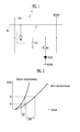
- FIG. 1 is a circuit diagram schematically showing a pixel 4 of a conventional organic light emitting display.
- the pixel 4 of the conventional organic light emitting display includes an organic light emitting diode (OLED) and a pixel circuit 2 coupled to a data line (Dm) and a scan line (Sn) to control the organic light emitting diode (OLED).
- OLED organic light emitting diode
- Dm data line
- Sn scan line
- An anode electrode of the organic light emitting diode (OLED) is coupled to the pixel circuit 2, and a cathode electrode thereof is coupled to the second power source (ELVSS).
- Such an organic light emitting diode (OLED) generates light with set (or predetermined) luminance to correspond to an electric current supplied from the pixel circuit 2.
- the pixel circuit 2 controls an electric current capacity supplied to the organic light emitting diode (OLED) to correspond to a data signal supplied to the data line (Dm) when a scan signal is supplied to the scan line (Sn).
- the pixel circuit 2 includes a second transistor (M2) coupled between the first power source (ELVDD) and the organic light emitting diode (OLED); a first transistor (M1) coupled between the second transistor (M2), and the data line (Dm) and the scan line (Sn); and a storage capacitor (Cst) coupled between a gate electrode of the second transistor (M2) and a first electrode of the second transistor (M2).
- a gate electrode of the first transistor (M1) is coupled to the scan line (Sn), and a first electrode of the first transistor (M1) is coupled to the data line (Dm).
- a second electrode of the first transistor (M1) is coupled to one side terminal of the storage capacitor (Cst).
- the first electrode of the first transistor (M1) is set to be a source electrode or a drain electrode, and the second electrode is set to be the other electrode that is different from the first electrode.
- the second electrode is set to be a drain electrode.
- the first transistor (M1) coupled to the scan line (Sn) and the data line (Dm), is turned on when a scan signal is supplied to the scan line (Sn), thereby supplying a data signal, supplied from the data line (Dm), to the storage capacitor (Cst). At this time, the storage capacitor (Cst) is charged with a voltage corresponding to the data signal.
- the gate electrode of the second transistor (M2) is coupled to one side terminal of the storage capacitor (Cst), and the first electrode of the second transistor (M2) is coupled to the other side terminal of the storage capacitor (Cst) and the first power source (ELVDD).
- a second electrode of the second transistor (M2) is coupled to an anode electrode of the organic light emitting diode (OLED).
- Such a second transistor (M2) controls a capacity of an electric current to correspond to the voltage value stored in the storage capacitor (Cst), the electric current flowing from the first power source (ELVDD) to the second power source (ELVSS) via the organic light emitting diode (OLED). At this time, the organic light emitting diode (OLED) generates light corresponding to the electric current capacity supplied from the second transistor (M2).
- the above-mentioned organic light emitting display has a problem in that it is difficult to display an image with desired luminance due to the changes in efficiency caused by the deterioration (or degradation) of the organic light emitting diode (OLED). That is, the organic light emitting diode (OLED) deteriorates with time, and therefore it is difficult to display the image with the desired luminance over time because an organic light emitting diode (OLED) that has deteriorated more generates light with lower luminance than that of an organic light emitting diode (OLED) that has deteriorated less.
- An aspect of an embodiment of the present invention is directed toward a pixel capable of compensating for the deterioration of an organic light emitting diode.
- Another aspect of an embodiment of the present invention is directed toward an organic light emitting display using the pixel.
- An embodiment of the present invention provides a pixel including an organic light emitting diode; a second transistor for controlling a capacity of an electric current that is supplied from a first power source to the organic light emitting diode; a first transistor coupled between a data line and a gate electrode of the second transistor and for turning on when a scan signal is supplied to a scan line; a first capacitor coupled between a power line for receiving a power signal and the gate electrode of the second transistor, the power signal overlapping with the scan signal and having a wider interval than that of the scan signal; and a feedback capacitor coupled between the gate electrode of the second transistor and an anode electrode of the organic light emitting diode.
- the pixel according to one embodiment of the present invention further includes a second capacitor coupled between the first power source and the gate electrode of the second transistor.
- Another embodiment of the present invention provides a pixel including an organic light emitting diode; a second transistor for controlling a capacity of an electric current supplied from a first power source to the organic light emitting diode; a first transistor coupled between a data line and a gate electrode of the second transistor and for turning on when a scan signal is supplied to a scan line; a first capacitor coupled between the scan line and the gate electrode of the second transistor; a second capacitor coupled between the first power source and the gate electrode of the second transistor; and a feedback capacitor coupled between the gate electrode of the second transistor and an anode electrode of the organic light emitting diode.
- an organic light emitting display including a scan driver for sequentially supplying a scan signal to scan lines; a power signal supply unit for sequentially supplying a power signal to power lines; a data driver for supplying a data signal to data lines to synchronize with the scan signal; and pixels at crossing regions of the scan lines, the data lines and the power lines.
- Each of the pixels extended in an i th (i is an integer) horizontal line of the organic light emitting display includes an organic light emitting diode; a second transistor for controlling a capacity of an electric current that is supplied from a first power source to the organic light emitting diode; a first transistor coupled between a corresponding data line of the data lines and a gate electrode of the second transistor and for turning on when the scan signal is supplied to an i th scan line of the scan lines; a first capacitor coupled between an i th power line of the power lines and the gate electrode of the second transistor; and a feedback capacitor coupled between the gate electrode of the second transistor and an anode electrode of the organic light emitting diode.
- a voltage of a third power source may be supplied to the i th power line when the power signal is supplied to the i th power line, and a voltage of a fourth power source that is higher than that of the third power source may be supplied to the i th power line when the power signal is not supplied to the i th power line.
- the voltages of the third power source and the fourth power source are set to a voltage value so that an electric current flows in the second transistor, the electric current being higher than an electric current that flows to correspond to the data signal.
- the power signal supply unit is adapted to supply the power signal to overlap with the scan signal supplied to the i th scan line, and to supply the power signal to the i th power line, the power signal having a wider interval than that of the scan signal.
- the data signal may be set to a voltage corresponding to a higher grey level than grey levels to be actually expressed.
- the organic light emitting display further comprises a second capacitor coupled between the first power source and the gate electrode of the second transistor.
- Another embodiment of the present invention provides an organic light emitting display including a scan driver for sequentially supplying a scan signal to scan lines; a data driver for supplying a data signal to data lines to synchronize with the scan signal; and pixels disposed at crossing regions of the scan lines and the data lines.
- Each of the pixels extended in an i th (i is an integer) horizontal line includes an organic light emitting diode; a second transistor for controlling a capacity of an electric current that is supplied from a first power source to the organic light emitting diode; a first transistor coupled between a corresponding data line of the data lines and a gate electrode of the second transistor and for turning on when the scan signal is supplied to an i th scan line of the scan lines; a first capacitor coupled between the i th scan line and the gate electrode of the second transistor; a second capacitor coupled between the first power source and the gate electrode of the second transistor; and a feedback capacitor coupled between the gate electrode of the second transistor and an anode electrode of the organic light emitting diode, and wherein i is an integer.
- a voltage of a third power source is supplied to the i th scan line when the scan signal is supplied to the i th scan line, and a voltage of a fourth power source that is higher than that of the third power source is supplied to the i th scan line when the scan signal is not supplied to the i th scan line.
- the voltages of the third power source and the fourth power source are set to a voltage value so that an electric current flows in the second transistor, the electric current being higher than an electric current that flows to correspond to the data signal.
- the data signal is set to a voltage corresponding to a higher grey level than grey levels to be actually expressed.
- FIG. 1 is a circuit diagram schematically showing a pixel of a conventional organic light emitting display.
- FIG. 2 is a graph illustrating the deterioration characteristics of an organic light emitting diode.
- FIG. 3 is a diagram schematically showing an organic light emitting display according to one exemplary embodiment of the present invention.
- FIG. 4 is a circuit diagram schematically showing a pixel according to a first exemplary embodiment as shown in FIG. 3 .
- FIG. 5 is a waveform view showing a method for driving the pixel as shown in FIG. 4 .
- FIG. 6 is a circuit diagram schematically showing a pixel according to a second exemplary embodiment as shown in FIG. 3 .
- FIG. 7 is a circuit diagram schematically showing a pixel according to a third exemplary embodiment as shown in FIG. 3 .
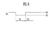
- FIG. 8 is a waveform view showing a method for driving the pixel as shown in FIG. 7 .
- first element when a first element is described as being coupled to a second element, the first element may be not only directly coupled to the second element but may also be indirectly coupled to the second element via a third element. Further, some of the elements that are not essential to the complete understanding of the invention are omitted for clarity. Also, like reference numerals refer to like elements throughout.
- FIG. 2 is a graph illustrating the deterioration characteristics of an organic light emitting diode.
- “loled” represents an electric current that flows in an organic light emitting diode
- “Voled” represents a voltage applied to the organic light emitting diode.
- a higher voltage is applied to an organic light emitting diode that is more deteriorated (after deterioration) to correspond to the same electric current of an organic light emitting diode that is less deteriorated (before deterioration).
- a voltage range (or difference) of ⁇ V1 corresponds to a certain electric current range (I1 to I2) before the organic light emitting diode is deteriorated.
- a voltage range of ⁇ V2 having a higher voltage range than the voltage range of ⁇ V1 corresponds to the certain electric current range (I1 to I2).
- resistance components of the organic light emitting diode are increased in number as the organic light emitting diode is further deteriorated.
- FIG. 3 is a diagram schematically showing an organic light emitting display according to one exemplary embodiment of the present invention.
- the organic light emitting display includes a pixel unit (or display region) 130 including pixels 140 disposed at (or in) regions (or crossing regions) divided (or defined) by scan lines (S1 to Sn), power lines (VL1 to VLn) and data lines (D1 to Dm); a scan driver 110 to drive the scan lines (S1 to Sn); a data driver 120 to drive the data lines (D1 to Dm); a power signal supply unit 160 to drive the power lines (VL1 to VLn); and a timing controller 150 to control the scan driver 110, the data driver 120, and the power signal supply unit 160.
- a pixel unit 130 including pixels 140 disposed at (or in) regions (or crossing regions) divided (or defined) by scan lines (S1 to Sn), power lines (VL1 to VLn) and data lines (D1 to Dm); a scan driver 110 to drive the scan lines (S1 to Sn); a data driver 120 to drive the data lines (D1 to Dm); a power signal supply unit 160 to drive
- the scan driver 110 generates a scan signal under the control of the timing controller 150, and sequentially supplies the generated scan signal to the scan lines (S1 to Sn).
- polarity of the scan signal is set to turn on a transistor in each of the pixels 140.
- the transistor in each of the pixels 140 is a P-channel metal-oxide semiconductor (PMOS)
- the polarity of the scan signal is set to a LOW voltage.
- the power signal supply unit 160 sequentially supplies a power signal to the power lines (VL1 to VLn).
- the power line (VL) receiving the power signal is set to a voltage of a third power source
- the power line (VL) that does not receive the power signal is set to a voltage of a fourth power source that is higher than that of the third power source.
- the power signal supplied to the i th power line (VLi) is overlapped with the scan signal supplied to the i th scan line (Si), and is also (concurrently or simultaneously) set to have a wider interval (or width) than that of the scan signal.
- the power signal supply unit 160 may be deleted by a designer.
- a voltage of the scan line (S) that receives a scan signal is set to a voltage value of the third power source, and a voltage of the scan line (S) that does not receive a scan signal is set to a voltage value of the fourth power source.
- the data driver 120 generates a data signal under the control of the timing controller 150, and supplies the generated data signal to the data lines (D1 to Dm) to synchronize with the scan signal.
- the timing controller 150 controls the scan driver 110, the data driver 120, and the power signal supply unit 160. Also, the timing controller 150 transmits externally supplied data to the data driver 120.
- the pixel unit 130 receives a power (or voltage) of a first power source (ELVDD) and a power (or voltage) of a second power source (ELVSS) from the outside of the pixel unit 130, and supplies the power of the first power source (ELVDD) and the power of the second power source (ELVSS) to each of the pixels 140.
- Each of the pixels 140 receiving the power of the first power source (ELVDD) and the power of the second power source (ELVSS) generates the light corresponding to the data signal.
- the above-mentioned pixels 140 function to generate light with desired luminance by compensating for the deterioration of an organic light emitting diode that is included in each of the pixels 140.
- a compensation unit to compensate for the deterioration of an organic light emitting diode is installed in each of the pixels 140.
- FIG. 4 is a circuit diagram schematically showing a pixel 140 according to a first exemplary embodiment as shown in FIG. 3 .
- a pixel coupled to an n th scan line (Sn) and an m th data line (Dm) is shown in FIG. 4 for convenience of the description.
- the pixel 140 includes an organic light emitting diode (OLED); a second transistor (M2) to supply an electric current to the organic light emitting diode (OLED); a first transistor (M1) to supply a data signal to the second transistor (M2); a storage capacitor (Cst) to store a voltage corresponding to the data signal; and a feedback capacitor (Cfb) to control a voltage of first node (N1) to correspond to the change in a voltage of the organic light emitting diode (OLED).
- OLED organic light emitting diode
- M2 to supply an electric current to the organic light emitting diode
- M1 to supply a data signal to the second transistor (M2)
- a storage capacitor (Cst) to store a voltage corresponding to the data signal
- a feedback capacitor (Cfb) to control a voltage of first node (N1) to correspond to the change in a voltage of the organic light emitting diode (OLED).
- An anode electrode of the organic light emitting diode (OLED) is coupled to a second electrode of the second transistor (M2), and a cathode electrode is coupled to the second power source (ELVSS).
- Such an organic light emitting diode (OLED) generates light with set (or predetermined) luminance to correspond to an electric current capacity supplied from the second transistor (M2).
- the first power source (ELVDD) has a higher voltage value than the second power source (ELVSS).
- a gate electrode of the first transistor (M1) is coupled to the scan line (Sn), and a first electrode of the first transistor (M1) is coupled to the data line (Dm).
- a second electrode of the first transistor (M1) is coupled to a gate electrode (i.e., a first node (N1)) of the second transistor (M2).
- Such a first transistor (M1) is turned on when a scan signal is supplied to the scan line (Sn), thereby supplying a data signal, supplied from the data line (Dm), to the first node (N1).
- a gate electrode of the second transistor (M2) is coupled to the first node (N1), and a first electrode of the second transistor (M2) is coupled to the first power source (ELVDD).
- a second electrode of the second transistor (M2) is coupled to an anode electrode of the organic light emitting diode (OLED).
- Such a second transistor (M2) supplies an electric current to the organic light emitting diode (OLED), the electric current corresponding to a voltage applied to the first node (N1).
- the storage capacitor (Cst) is coupled between the first node (N1) and the power line (VLn). Such a storage capacitor (Cst) is charged with a voltage corresponding to the data signal.
- the feedback capacitor (Cfb) is coupled between the first node (N1) and the anode electrode of the organic light emitting diode (OLED). Such a feedback capacitor (Cfb) controls a voltage of the first node (N1) to correspond to the changed voltage capacity of the organic light emitting diode (OLED).
- FIG. 5 is a waveform view showing a method for driving the pixel 140 as shown in FIG. 4 .
- a power signal is supplied to a power line (VLn) during a first period (T1).
- a voltage of the power line (VLn) drops from a voltage (V4) of the fourth power source to a voltage (V3) of the third power source.
- a voltage of the first node (N1) drops to correspond to the voltage drop of the power line (VLn) due to the coupling of the storage capacitor (Cst).
- the voltage (V3) of the third power source and the voltage (V4) of the fourth power source are set so that a high first electric current can flow from the second transistor (M2) to the organic light emitting diode (OLED).
- the voltage (V3) of the third power source and the voltage (V4) of the fourth power source are set so that an electric current, which is higher than the maximum electric current that may flow in the organic light emitting diode (OLED), can flow to correspond to the data signal.
- a voltage corresponding to the first electric current is applied to the organic light emitting diode (OLED) that receives the first electric current from the second transistor (M2).
- the feedback capacitor (Cfb) is charged with a voltage corresponding to the voltage difference between the voltage applied to the organic light emitting diode (OLED) and the voltage applied to the first node (N1).
- a scan signal is supplied to the scan line (Sn).
- the first transistor (M1) is turned on.
- a data signal supplied to the data line (Dm) is supplied to the first node (N1).
- the storage capacitor (Cst) is charged with a voltage corresponding to the data signal.
- the data signal is supplied to correspond to a higher grey level (i.e., to allow a more emission electric current to flow) than grey levels to be actually expressed so as to supply an electric current corresponding to the normal grey levels, when a voltage of the power line (VLn) increases afterwards.
- the supply of a scan signal to the scan line (Sn) is suspended during a third period (T3).
- the first transistor (M1) is turned off.
- the feedback capacitor (Cfb) is continuously charged with a voltage that is applied to correspond to the first electric current supplied to the organic light emitting diode (OLED).
- the first electric current refers to an electric current corresponding to the voltage drop of the data signal and power line (VLn).
- the supply of a power signal supplied to the power line (VLn) is suspended during a fourth period (T4).
- a voltage of the power line (VLn) increases from the voltage (V3) of the third power source to the voltage (V4) of the fourth power source.
- a voltage of the first node (N1) also increases according to the voltage swell of the power line (VLn) because the first node (N1) is set to be in a floating state.
- the second transistor (M2) supplies a second electric current to the organic light emitting diode (OLED) to correspond to the voltage swell of the first node (N1), the second electric current being lower than the first electric current.
- a voltage corresponding to the second electric current is applied to the organic light emitting diode (OLED) that receives the second electric current from the second transistor (M2).
- a voltage applied to the organic light emitting diode (OLED) is set to a lower voltage value during the fourth period (T4), compared to the voltage as in the third period (T3) because the second electric current is an electric current that is lower than the first electric current.
- the voltage of the first node (N1) which is set to be in the floating state, is changed according to the voltage applied to the organic light emitting diode (OLED).
- the voltage of the first node (N1) is changed as represented by the following Equation 1.
- V N ⁇ 1 Vdata - Cfd ⁇ Voled ⁇ 1 - Voled ⁇ 2 / Cst + Cfb
- Voled1 represents a voltage that is applied to the organic light emitting diode (OLED) to correspond to the first electric current
- Voled2 represents a voltage that is applied to the organic light emitting diode (OLED) to correspond to the second electric current
- Vdata represents a voltage corresponding to the data signal.
- Equation 1 it is revealed that the voltage of the first node (N1) is changed when the voltage applied to the organic light emitting diode (OLED) is changed.
- a voltage value of Voled1 - Voled2 is increased due to the increased in the resistance of the organic light emitting diode (OLED), which leads to the increased voltage drop range of the first node (N1). That is, the capacity of an electric current that flows in the second transistor (M2) is increased to correspond to the same data signal when the organic light emitting diode (OLED) is deteriorated in the first exemplary embodiment of the present invention. Therefore, it is possible to compensate for the deterioration of the organic light emitting diode (OLED).
- FIG. 6 is a circuit diagram schematically showing a pixel 140' according to a second exemplary embodiment of the present invention. The detailed description of the same components as in FIG. 4 is omitted for clarity purposes.
- the storage capacitor (Cst) is coupled between the first power source (ELVDD) and the first node (N1) for the pixel 140' according to the second exemplary embodiment of the present invention. Such a storage capacitor (Cst) is charged with a voltage corresponding to the data signal.
- a boosting capacitor (Cb) coupled between the power line (VLn) and the first node (N1) is further provided in the pixel 140' according to the second exemplary embodiment of the present invention. That is, the voltage of the first node (N1) is changed using the storage capacitor (Cst) in the case of the pixel 140 as shown in FIG. 4 , but the voltage of the first node (N1) is changed using a separate boosting capacitor (Cb) in the case of the pixel 140' as shown in FIG. 6 .
- the other procedures of the method according to the present invention are identical (or substantially identical) to that of the pixel 140 as shown in FIG. 4 , and therefore the detailed description of the other procedures is omitted for clarity purposes.
- FIG. 7 is a circuit diagram schematically showing a pixel 140" according to a third exemplary embodiment of the present invention. The detailed description of the same components as in FIG. 6 is omitted for clarity purposes.
- a boosting capacitor (Cb) is coupled between the scan line (Sn) and the first node (N1). Such a boosting capacitor (Cb) changes a voltage of the first node (N1) to correspond to the scan signal supplied to the scan line (Sn).
- FIG. 8 is a waveform view showing a method for driving the pixel 140" as shown in FIG. 7 .
- a scan signal is supplied to the scan line (Sn) during a first period (T1).
- the first transistor (M1) When the scan signal is supplied to the scan line (Sn), the first transistor (M1) is turned on. When the first transistor (M1) is turned on, a data signal is supplied to the first node (N1). When the scan signal is supplied to the scan line (Sn), a voltage of the scan line (Sn) drops from the voltage (V4) of the fourth power source to the voltage (V3) of the third power source. At this time, a voltage of the first node (N1) also drops by utilizing the boosting capacitor (Cb) to correspond to the voltage drop of the scan line (Sn).
- the first electric current refers to an electric current corresponding to the voltage drop of the data signal and scan line (Sn).
- a voltage corresponding to the first electric current is applied to the organic light emitting diode (OLED) during the first period (T1). At this time, a voltage corresponding to the voltage difference between the voltage applied to the organic light emitting diode (OLED) and the voltage applied to the first node (N1) is charged in the feedback capacitor (Cfb).
- the supply of the scan signal to the scan line (Sn) is suspended during a second period (T2).
- the first transistor (M1) is turned off.
- a voltage of the scan line (Sn) increases from the voltage (V3) of the third power source to the voltage (V4) of the fourth power source.
- the voltage of the first node (N1) also increases to correspond to the voltage swell of the scan line (Sn) because the first node (N1) is set to be in a floating state.
- the second transistor (M2) supplies a second electric current to the organic light emitting diode (OLED) to correspond to the voltage of the first node (N1), the second electric current being lower than the first electric current.
- a voltage corresponding to the second electric current is applied to the organic light emitting diode (OLED) that receives the second electric current from the second transistor (M2).
- a voltage applied to the organic light emitting diode (OLED) during the second period (T2) is set to a lower voltage value than the voltage as in the first period (T1) because the second electric current is an electric current that is lower than the first electric current.
- the voltage of the first node (N1) which is set to be in the floating state, is changed according to the voltage applied to the organic light emitting diode (OLED). That is, the voltage applied to the first node (N1) is changed according to the voltage applied to the organic light emitting diode (OLED).
- the difference in the voltage applied to the organic light emitting diode (OLED) is increased to correspond to the first electric current and the second electric current, which leads to the increased voltage drop range of the first node (N1).
- an electric current that flows form the second transistor (M2) is increased to correspond to the same data signal when the organic light emitting diode (OLED) is deteriorated in the third exemplary embodiment of the present invention. Therefore, it is possible to compensate for the deterioration of the organic light emitting diode (OLED).
Landscapes
- Engineering & Computer Science (AREA)
- Physics & Mathematics (AREA)
- Computer Hardware Design (AREA)
- General Physics & Mathematics (AREA)
- Theoretical Computer Science (AREA)
- Electroluminescent Light Sources (AREA)
- Control Of El Displays (AREA)
- Control Of Indicators Other Than Cathode Ray Tubes (AREA)
Applications Claiming Priority (1)
| Application Number | Priority Date | Filing Date | Title |
|---|---|---|---|
| KR1020080021973A KR100911978B1 (ko) | 2008-03-10 | 2008-03-10 | 화소 및 이를 이용한 유기전계발광 표시장치 |
Publications (2)
| Publication Number | Publication Date |
|---|---|
| EP2104091A1 true EP2104091A1 (de) | 2009-09-23 |
| EP2104091B1 EP2104091B1 (de) | 2011-10-26 |
Family
ID=40466189
Family Applications (1)
| Application Number | Title | Priority Date | Filing Date |
|---|---|---|---|
| EP09154277A Active EP2104091B1 (de) | 2008-03-10 | 2009-03-04 | Pixelschaltung eines OLED-Displays mit OLED-Alterungskompensation |
Country Status (5)
| Country | Link |
|---|---|
| US (1) | US8310417B2 (de) |
| EP (1) | EP2104091B1 (de) |
| JP (1) | JP4871936B2 (de) |
| KR (1) | KR100911978B1 (de) |
| CN (1) | CN101533851B (de) |
Families Citing this family (23)
| Publication number | Priority date | Publication date | Assignee | Title |
|---|---|---|---|---|
| JP5067134B2 (ja) * | 2007-11-13 | 2012-11-07 | ソニー株式会社 | 表示装置及び表示装置の駆動方法 |
| KR101056240B1 (ko) * | 2009-03-02 | 2011-08-11 | 삼성모바일디스플레이주식회사 | 유기전계발광 표시장치 |
| US10680515B2 (en) | 2011-05-05 | 2020-06-09 | Psemi Corporation | Power converters with modular stages |
| KR101556838B1 (ko) | 2011-05-05 | 2015-10-13 | 아크틱 샌드 테크놀로지스, 인크. | 모듈형 단계들을 구비한 dc-dc 컨버터 |
| JP5909759B2 (ja) * | 2011-09-07 | 2016-04-27 | 株式会社Joled | 画素回路、表示パネル、表示装置および電子機器 |
| US8743553B2 (en) | 2011-10-18 | 2014-06-03 | Arctic Sand Technologies, Inc. | Power converters with integrated capacitors |
| KR101882297B1 (ko) * | 2012-02-03 | 2018-07-30 | 삼성디스플레이 주식회사 | 화소 및 이를 이용한 유기전계발광 표시장치 |
| KR20140081262A (ko) * | 2012-12-21 | 2014-07-01 | 삼성디스플레이 주식회사 | 화소 및 이를 이용한 유기전계발광 표시장치 |
| US8724353B1 (en) | 2013-03-15 | 2014-05-13 | Arctic Sand Technologies, Inc. | Efficient gate drivers for switched capacitor converters |
| US8619445B1 (en) | 2013-03-15 | 2013-12-31 | Arctic Sand Technologies, Inc. | Protection of switched capacitor power converter |
| JP2015025978A (ja) * | 2013-07-26 | 2015-02-05 | 株式会社ジャパンディスプレイ | 駆動回路、表示装置、及び駆動方法 |
| KR102226422B1 (ko) * | 2014-10-13 | 2021-03-12 | 삼성디스플레이 주식회사 | 유기 발광 표시 장치 및 이의 구동 방법 |
| TW201640796A (zh) | 2015-03-13 | 2016-11-16 | 亞提克聖德技術股份有限公司 | 具有用於促進電容器間絕能耗電荷傳輸的電感器之直流對直流變壓器 |
| WO2017007991A1 (en) | 2015-07-08 | 2017-01-12 | Arctic Sand Technologies, Inc. | Switched-capacitor power converters |
| CN106097963B (zh) * | 2016-08-19 | 2018-07-06 | 京东方科技集团股份有限公司 | 电路结构、显示设备及驱动方法 |
| KR102660207B1 (ko) * | 2017-02-09 | 2024-04-25 | 삼성디스플레이 주식회사 | 화소 및 이를 포함하는 표시 장치 |
| CN108777130A (zh) | 2018-06-21 | 2018-11-09 | 京东方科技集团股份有限公司 | 像素电路及显示装置 |
| CN110491326A (zh) * | 2019-08-28 | 2019-11-22 | 深圳市华星光电半导体显示技术有限公司 | 像素电路、显示面板及显示装置 |
| CN110706650A (zh) * | 2019-09-17 | 2020-01-17 | 深圳市华星光电半导体显示技术有限公司 | 像素驱动电路 |
| CN111063305A (zh) * | 2020-01-07 | 2020-04-24 | 深圳市华星光电半导体显示技术有限公司 | 像素电路、显示面板及像素电路基准电压的补偿方法 |
| KR102767662B1 (ko) * | 2020-06-10 | 2025-02-18 | 삼성디스플레이 주식회사 | 개구율 계측 장치 및 이를 포함하는 표시 장치의 열화 보상 시스템 |
| CN117672132A (zh) * | 2022-08-23 | 2024-03-08 | 京东方科技集团股份有限公司 | 像素电路及其驱动方法和显示面板、显示装置 |
| KR20240120066A (ko) * | 2023-01-31 | 2024-08-07 | 엘지디스플레이 주식회사 | 픽셀 회로 및 이를 포함하는 표시 장치 |
Citations (3)
| Publication number | Priority date | Publication date | Assignee | Title |
|---|---|---|---|---|
| US20050269958A1 (en) * | 2004-04-07 | 2005-12-08 | Choi Joon-Hoo | Display device and driving method thereof |
| US20060012549A1 (en) * | 2004-07-16 | 2006-01-19 | Kyoji Ikeda | Semiconductor device, display apparatus, and display apparatus driving method |
| EP1860637A2 (de) * | 2006-05-22 | 2007-11-28 | Sony Corporation | Anzeigevorrichtung und Steuerungsverfahren dafür |
Family Cites Families (22)
| Publication number | Priority date | Publication date | Assignee | Title |
|---|---|---|---|---|
| KR100452114B1 (ko) | 2002-04-15 | 2004-10-12 | 한국과학기술원 | 화소 회로 및 이를 이용한 유기 발광 다이오드 표시장치 |
| US7109952B2 (en) * | 2002-06-11 | 2006-09-19 | Samsung Sdi Co., Ltd. | Light emitting display, light emitting display panel, and driving method thereof |
| JP4467910B2 (ja) * | 2003-05-16 | 2010-05-26 | 東芝モバイルディスプレイ株式会社 | アクティブマトリクス型表示装置 |
| JP4826870B2 (ja) | 2003-12-02 | 2011-11-30 | ソニー株式会社 | 画素回路及びその駆動方法とアクティブマトリクス装置並びに表示装置 |
| JP4561096B2 (ja) * | 2003-12-26 | 2010-10-13 | ソニー株式会社 | ディスプレイ装置 |
| KR100579193B1 (ko) | 2004-01-12 | 2006-05-11 | 삼성에스디아이 주식회사 | 유기전계발광 표시장치 |
| KR100658616B1 (ko) * | 2004-05-31 | 2006-12-15 | 삼성에스디아이 주식회사 | 발광 표시 장치 및 그 표시 패널과 구동 방법 |
| TWI263186B (en) | 2004-07-16 | 2006-10-01 | Sanyo Electric Co | Semiconductor device, display device and driving method of display device |
| TWI282537B (en) * | 2005-04-21 | 2007-06-11 | Au Optronics Corp | Display units |
| JP2007011218A (ja) | 2005-07-04 | 2007-01-18 | Sharp Corp | 表示装置 |
| KR100679717B1 (ko) | 2005-07-25 | 2007-02-06 | 재단법인서울대학교산학협력재단 | 유기발광 표시장치의 화소 회로 |
| JP2007264464A (ja) * | 2006-03-29 | 2007-10-11 | Sanyo Electric Co Ltd | 有機エレクトロルミネッセンス表示装置の駆動方法および有機エレクトロルミネッセンス表示装置 |
| KR100805597B1 (ko) * | 2006-08-30 | 2008-02-20 | 삼성에스디아이 주식회사 | 화소 및 이를 이용한 유기전계발광 표시장치 및 그의구동방법 |
| KR20080020355A (ko) * | 2006-08-31 | 2008-03-05 | 삼성에스디아이 주식회사 | 유기전계발광표시장치 및 그의 구동방법 |
| KR100815754B1 (ko) * | 2006-11-09 | 2008-03-20 | 삼성에스디아이 주식회사 | 구동회로 및 이를 이용한 유기전계발광표시장치 |
| KR100812037B1 (ko) * | 2006-12-19 | 2008-03-10 | 삼성에스디아이 주식회사 | 유기전계발광 표시장치 |
| KR100821046B1 (ko) * | 2006-12-19 | 2008-04-08 | 삼성에스디아이 주식회사 | 화소 및 이를 이용한 유기전계발광 표시장치 |
| KR100821055B1 (ko) * | 2006-12-27 | 2008-04-08 | 삼성에스디아이 주식회사 | 유기전계발광 표시장치와 그의 구동방법 |
| KR101410465B1 (ko) * | 2007-02-22 | 2014-06-23 | 삼성디스플레이 주식회사 | 백라이트 장치 및 이를 갖는 액정표시장치 |
| JP2008209886A (ja) * | 2007-02-23 | 2008-09-11 | Samsung Sdi Co Ltd | 有機電界発光表示装置及びその駆動方法 |
| KR100858614B1 (ko) * | 2007-03-08 | 2008-09-17 | 삼성에스디아이 주식회사 | 유기전계발광표시장치 및 그의 구동방법 |
| KR100873076B1 (ko) * | 2007-03-14 | 2008-12-09 | 삼성모바일디스플레이주식회사 | 화소 및 이를 이용한 유기전계발광 표시장치 및 그의구동방법 |
-
2008
- 2008-03-10 KR KR1020080021973A patent/KR100911978B1/ko active Active
- 2008-09-29 JP JP2008249910A patent/JP4871936B2/ja active Active
- 2008-12-23 US US12/343,203 patent/US8310417B2/en active Active
-
2009
- 2009-03-04 CN CN2009100044719A patent/CN101533851B/zh active Active
- 2009-03-04 EP EP09154277A patent/EP2104091B1/de active Active
Patent Citations (3)
| Publication number | Priority date | Publication date | Assignee | Title |
|---|---|---|---|---|
| US20050269958A1 (en) * | 2004-04-07 | 2005-12-08 | Choi Joon-Hoo | Display device and driving method thereof |
| US20060012549A1 (en) * | 2004-07-16 | 2006-01-19 | Kyoji Ikeda | Semiconductor device, display apparatus, and display apparatus driving method |
| EP1860637A2 (de) * | 2006-05-22 | 2007-11-28 | Sony Corporation | Anzeigevorrichtung und Steuerungsverfahren dafür |
Also Published As
| Publication number | Publication date |
|---|---|
| US20090225012A1 (en) | 2009-09-10 |
| CN101533851B (zh) | 2011-06-29 |
| KR100911978B1 (ko) | 2009-08-13 |
| CN101533851A (zh) | 2009-09-16 |
| JP2009217237A (ja) | 2009-09-24 |
| JP4871936B2 (ja) | 2012-02-08 |
| EP2104091B1 (de) | 2011-10-26 |
| US8310417B2 (en) | 2012-11-13 |
Similar Documents
| Publication | Publication Date | Title |
|---|---|---|
| EP2104091A1 (de) | Pixelschaltung eines OLED-Displays mit OLED-Alterungskompensation | |
| US8194012B2 (en) | Pixel and organic light emitting display using the same | |
| EP2219174B1 (de) | Pixel und organische lichtemittierende Anzeigevorrichtung damit | |
| EP2192571B1 (de) | Organische lichtemittierende Anzeigevorrichtung und Antriebsverfahren dafür | |
| EP2136352B1 (de) | Pixel und organische Licht-emittierende Anzeigevorrichtung mit Kompensierung für Alterung des organischen Licht-emittierenden Elementes | |
| EP2261884B1 (de) | Pixel einer OLED Anzeige und entsprechende Anzeige | |
| US8587578B2 (en) | Pixel and organic light emitting display device | |
| EP2242039B1 (de) | Pixel und organische lichtemittierende Anzeigevorrichtung damit | |
| EP2410508B1 (de) | Pixel und organische lichtemittierende Anzeige damit | |
| US8446344B2 (en) | Pixel and organic light emitting display device using the same | |
| JP5582645B2 (ja) | 有機発光表示装置およびその駆動方法 | |
| KR100926618B1 (ko) | 화소 및 이를 이용한 유기전계발광 표시장치 | |
| US9262962B2 (en) | Pixel and organic light emitting display device using the same | |
| KR101142729B1 (ko) | 화소 및 이를 이용한 유기전계발광 표시장치 | |
| US8638279B2 (en) | Pixel and organic light emitting display device using the same | |
| US7847760B2 (en) | Pixel circuit, organic light emitting display using the pixel circuit and driving method for the display | |
| EP2192570A1 (de) | Pixel und damit versehene organische lichtemittierende Anzeigevorrichtung | |
| KR100628277B1 (ko) | 유기전계발광표시장치 및 이의 구동방법 |
Legal Events
| Date | Code | Title | Description |
|---|---|---|---|
| PUAI | Public reference made under article 153(3) epc to a published international application that has entered the european phase |
Free format text: ORIGINAL CODE: 0009012 |
|
| 17P | Request for examination filed |
Effective date: 20090304 |
|
| AK | Designated contracting states |
Kind code of ref document: A1 Designated state(s): AT BE BG CH CY CZ DE DK EE ES FI FR GB GR HR HU IE IS IT LI LT LU LV MC MK MT NL NO PL PT RO SE SI SK TR |
|
| AX | Request for extension of the european patent |
Extension state: AL BA RS |
|
| 17Q | First examination report despatched |
Effective date: 20091009 |
|
| AKX | Designation fees paid |
Designated state(s): DE FR GB |
|
| GRAC | Information related to communication of intention to grant a patent modified |
Free format text: ORIGINAL CODE: EPIDOSCIGR1 |
|
| GRAP | Despatch of communication of intention to grant a patent |
Free format text: ORIGINAL CODE: EPIDOSNIGR1 |
|
| RIN1 | Information on inventor provided before grant (corrected) |
Inventor name: CHOI, SANG-MOO |
|
| GRAS | Grant fee paid |
Free format text: ORIGINAL CODE: EPIDOSNIGR3 |
|
| GRAA | (expected) grant |
Free format text: ORIGINAL CODE: 0009210 |
|
| AK | Designated contracting states |
Kind code of ref document: B1 Designated state(s): DE FR GB |
|
| REG | Reference to a national code |
Ref country code: GB Ref legal event code: FG4D |
|
| REG | Reference to a national code |
Ref country code: DE Ref legal event code: R096 Ref document number: 602009003243 Country of ref document: DE Effective date: 20111222 |
|
| PLBE | No opposition filed within time limit |
Free format text: ORIGINAL CODE: 0009261 |
|
| STAA | Information on the status of an ep patent application or granted ep patent |
Free format text: STATUS: NO OPPOSITION FILED WITHIN TIME LIMIT |
|
| 26N | No opposition filed |
Effective date: 20120727 |
|
| REG | Reference to a national code |
Ref country code: DE Ref legal event code: R097 Ref document number: 602009003243 Country of ref document: DE Effective date: 20120727 |
|
| REG | Reference to a national code |
Ref country code: GB Ref legal event code: 732E Free format text: REGISTERED BETWEEN 20130103 AND 20130109 |
|
| REG | Reference to a national code |
Ref country code: DE Ref legal event code: R082 Ref document number: 602009003243 Country of ref document: DE Representative=s name: GULDE HENGELHAUPT ZIEBIG & SCHNEIDER, DE |
|
| REG | Reference to a national code |
Ref country code: DE Ref legal event code: R081 Ref document number: 602009003243 Country of ref document: DE Owner name: SAMSUNG DISPLAY CO., LTD., KR Free format text: FORMER OWNER: SAMSUNG MOBILE DISPLAY CO. LTD., SUWON, KR Effective date: 20130416 Ref country code: DE Ref legal event code: R082 Ref document number: 602009003243 Country of ref document: DE Representative=s name: GULDE HENGELHAUPT ZIEBIG & SCHNEIDER, DE Effective date: 20130416 Ref country code: DE Ref legal event code: R082 Ref document number: 602009003243 Country of ref document: DE Representative=s name: GULDE & PARTNER PATENT- UND RECHTSANWALTSKANZL, DE Effective date: 20130416 Ref country code: DE Ref legal event code: R081 Ref document number: 602009003243 Country of ref document: DE Owner name: SAMSUNG DISPLAY CO., LTD., YONGIN-CITY, KR Free format text: FORMER OWNER: SAMSUNG MOBILE DISPLAY CO. LTD., SUWON, GYEONGGI, KR Effective date: 20130416 |
|
| REG | Reference to a national code |
Ref country code: FR Ref legal event code: PLFP Year of fee payment: 8 |
|
| REG | Reference to a national code |
Ref country code: FR Ref legal event code: PLFP Year of fee payment: 9 |
|
| REG | Reference to a national code |
Ref country code: FR Ref legal event code: PLFP Year of fee payment: 10 |
|
| P01 | Opt-out of the competence of the unified patent court (upc) registered |
Effective date: 20230516 |
|
| PGFP | Annual fee paid to national office [announced via postgrant information from national office to epo] |
Ref country code: GB Payment date: 20260224 Year of fee payment: 18 |
|
| PGFP | Annual fee paid to national office [announced via postgrant information from national office to epo] |
Ref country code: DE Payment date: 20260220 Year of fee payment: 18 |
|
| PGFP | Annual fee paid to national office [announced via postgrant information from national office to epo] |
Ref country code: FR Payment date: 20260224 Year of fee payment: 18 |