EP2096679A1 - Method for manufacturing solar cell and apparatus for manufacturing solar cell - Google Patents
Method for manufacturing solar cell and apparatus for manufacturing solar cell Download PDFInfo
- Publication number
- EP2096679A1 EP2096679A1 EP07831279A EP07831279A EP2096679A1 EP 2096679 A1 EP2096679 A1 EP 2096679A1 EP 07831279 A EP07831279 A EP 07831279A EP 07831279 A EP07831279 A EP 07831279A EP 2096679 A1 EP2096679 A1 EP 2096679A1
- Authority
- EP
- European Patent Office
- Prior art keywords
- solar cell
- passivation film
- cell manufacturing
- plasma
- silicon layer
- Prior art date
- Legal status (The legal status is an assumption and is not a legal conclusion. Google has not performed a legal analysis and makes no representation as to the accuracy of the status listed.)
- Withdrawn
Links
Images



Classifications
-
- H—ELECTRICITY
- H10—SEMICONDUCTOR DEVICES; ELECTRIC SOLID-STATE DEVICES NOT OTHERWISE PROVIDED FOR
- H10F—INORGANIC SEMICONDUCTOR DEVICES SENSITIVE TO INFRARED RADIATION, LIGHT, ELECTROMAGNETIC RADIATION OF SHORTER WAVELENGTH OR CORPUSCULAR RADIATION
- H10F71/00—Manufacture or treatment of devices covered by this subclass
- H10F71/129—Passivating
-
- C—CHEMISTRY; METALLURGY
- C23—COATING METALLIC MATERIAL; COATING MATERIAL WITH METALLIC MATERIAL; CHEMICAL SURFACE TREATMENT; DIFFUSION TREATMENT OF METALLIC MATERIAL; COATING BY VACUUM EVAPORATION, BY SPUTTERING, BY ION IMPLANTATION OR BY CHEMICAL VAPOUR DEPOSITION, IN GENERAL; INHIBITING CORROSION OF METALLIC MATERIAL OR INCRUSTATION IN GENERAL
- C23C—COATING METALLIC MATERIAL; COATING MATERIAL WITH METALLIC MATERIAL; SURFACE TREATMENT OF METALLIC MATERIAL BY DIFFUSION INTO THE SURFACE, BY CHEMICAL CONVERSION OR SUBSTITUTION; COATING BY VACUUM EVAPORATION, BY SPUTTERING, BY ION IMPLANTATION OR BY CHEMICAL VAPOUR DEPOSITION, IN GENERAL
- C23C16/00—Chemical coating by decomposition of gaseous compounds, without leaving reaction products of surface material in the coating, i.e. chemical vapour deposition [CVD] processes
- C23C16/02—Pretreatment of the material to be coated
- C23C16/0209—Pretreatment of the material to be coated by heating
- C23C16/0218—Pretreatment of the material to be coated by heating in a reactive atmosphere
-
- C—CHEMISTRY; METALLURGY
- C23—COATING METALLIC MATERIAL; COATING MATERIAL WITH METALLIC MATERIAL; CHEMICAL SURFACE TREATMENT; DIFFUSION TREATMENT OF METALLIC MATERIAL; COATING BY VACUUM EVAPORATION, BY SPUTTERING, BY ION IMPLANTATION OR BY CHEMICAL VAPOUR DEPOSITION, IN GENERAL; INHIBITING CORROSION OF METALLIC MATERIAL OR INCRUSTATION IN GENERAL
- C23C—COATING METALLIC MATERIAL; COATING MATERIAL WITH METALLIC MATERIAL; SURFACE TREATMENT OF METALLIC MATERIAL BY DIFFUSION INTO THE SURFACE, BY CHEMICAL CONVERSION OR SUBSTITUTION; COATING BY VACUUM EVAPORATION, BY SPUTTERING, BY ION IMPLANTATION OR BY CHEMICAL VAPOUR DEPOSITION, IN GENERAL
- C23C16/00—Chemical coating by decomposition of gaseous compounds, without leaving reaction products of surface material in the coating, i.e. chemical vapour deposition [CVD] processes
- C23C16/22—Chemical coating by decomposition of gaseous compounds, without leaving reaction products of surface material in the coating, i.e. chemical vapour deposition [CVD] processes characterised by the deposition of inorganic material, other than metallic material
- C23C16/30—Deposition of compounds, mixtures or solid solutions, e.g. borides, carbides, nitrides
- C23C16/308—Oxynitrides
-
- C—CHEMISTRY; METALLURGY
- C23—COATING METALLIC MATERIAL; COATING MATERIAL WITH METALLIC MATERIAL; CHEMICAL SURFACE TREATMENT; DIFFUSION TREATMENT OF METALLIC MATERIAL; COATING BY VACUUM EVAPORATION, BY SPUTTERING, BY ION IMPLANTATION OR BY CHEMICAL VAPOUR DEPOSITION, IN GENERAL; INHIBITING CORROSION OF METALLIC MATERIAL OR INCRUSTATION IN GENERAL
- C23C—COATING METALLIC MATERIAL; COATING MATERIAL WITH METALLIC MATERIAL; SURFACE TREATMENT OF METALLIC MATERIAL BY DIFFUSION INTO THE SURFACE, BY CHEMICAL CONVERSION OR SUBSTITUTION; COATING BY VACUUM EVAPORATION, BY SPUTTERING, BY ION IMPLANTATION OR BY CHEMICAL VAPOUR DEPOSITION, IN GENERAL
- C23C16/00—Chemical coating by decomposition of gaseous compounds, without leaving reaction products of surface material in the coating, i.e. chemical vapour deposition [CVD] processes
- C23C16/22—Chemical coating by decomposition of gaseous compounds, without leaving reaction products of surface material in the coating, i.e. chemical vapour deposition [CVD] processes characterised by the deposition of inorganic material, other than metallic material
- C23C16/30—Deposition of compounds, mixtures or solid solutions, e.g. borides, carbides, nitrides
- C23C16/34—Nitrides
- C23C16/345—Silicon nitride
-
- C—CHEMISTRY; METALLURGY
- C23—COATING METALLIC MATERIAL; COATING MATERIAL WITH METALLIC MATERIAL; CHEMICAL SURFACE TREATMENT; DIFFUSION TREATMENT OF METALLIC MATERIAL; COATING BY VACUUM EVAPORATION, BY SPUTTERING, BY ION IMPLANTATION OR BY CHEMICAL VAPOUR DEPOSITION, IN GENERAL; INHIBITING CORROSION OF METALLIC MATERIAL OR INCRUSTATION IN GENERAL
- C23C—COATING METALLIC MATERIAL; COATING MATERIAL WITH METALLIC MATERIAL; SURFACE TREATMENT OF METALLIC MATERIAL BY DIFFUSION INTO THE SURFACE, BY CHEMICAL CONVERSION OR SUBSTITUTION; COATING BY VACUUM EVAPORATION, BY SPUTTERING, BY ION IMPLANTATION OR BY CHEMICAL VAPOUR DEPOSITION, IN GENERAL
- C23C16/00—Chemical coating by decomposition of gaseous compounds, without leaving reaction products of surface material in the coating, i.e. chemical vapour deposition [CVD] processes
- C23C16/22—Chemical coating by decomposition of gaseous compounds, without leaving reaction products of surface material in the coating, i.e. chemical vapour deposition [CVD] processes characterised by the deposition of inorganic material, other than metallic material
- C23C16/30—Deposition of compounds, mixtures or solid solutions, e.g. borides, carbides, nitrides
- C23C16/40—Oxides
- C23C16/401—Oxides containing silicon
-
- C—CHEMISTRY; METALLURGY
- C23—COATING METALLIC MATERIAL; COATING MATERIAL WITH METALLIC MATERIAL; CHEMICAL SURFACE TREATMENT; DIFFUSION TREATMENT OF METALLIC MATERIAL; COATING BY VACUUM EVAPORATION, BY SPUTTERING, BY ION IMPLANTATION OR BY CHEMICAL VAPOUR DEPOSITION, IN GENERAL; INHIBITING CORROSION OF METALLIC MATERIAL OR INCRUSTATION IN GENERAL
- C23C—COATING METALLIC MATERIAL; COATING MATERIAL WITH METALLIC MATERIAL; SURFACE TREATMENT OF METALLIC MATERIAL BY DIFFUSION INTO THE SURFACE, BY CHEMICAL CONVERSION OR SUBSTITUTION; COATING BY VACUUM EVAPORATION, BY SPUTTERING, BY ION IMPLANTATION OR BY CHEMICAL VAPOUR DEPOSITION, IN GENERAL
- C23C16/00—Chemical coating by decomposition of gaseous compounds, without leaving reaction products of surface material in the coating, i.e. chemical vapour deposition [CVD] processes
- C23C16/44—Chemical coating by decomposition of gaseous compounds, without leaving reaction products of surface material in the coating, i.e. chemical vapour deposition [CVD] processes characterised by the method of coating
- C23C16/50—Chemical coating by decomposition of gaseous compounds, without leaving reaction products of surface material in the coating, i.e. chemical vapour deposition [CVD] processes characterised by the method of coating using electric discharges
- C23C16/511—Chemical coating by decomposition of gaseous compounds, without leaving reaction products of surface material in the coating, i.e. chemical vapour deposition [CVD] processes characterised by the method of coating using electric discharges using microwave discharges
-
- H—ELECTRICITY
- H10—SEMICONDUCTOR DEVICES; ELECTRIC SOLID-STATE DEVICES NOT OTHERWISE PROVIDED FOR
- H10F—INORGANIC SEMICONDUCTOR DEVICES SENSITIVE TO INFRARED RADIATION, LIGHT, ELECTROMAGNETIC RADIATION OF SHORTER WAVELENGTH OR CORPUSCULAR RADIATION
- H10F10/00—Individual photovoltaic cells, e.g. solar cells
- H10F10/10—Individual photovoltaic cells, e.g. solar cells having potential barriers
- H10F10/14—Photovoltaic cells having only PN homojunction potential barriers
-
- H—ELECTRICITY
- H10—SEMICONDUCTOR DEVICES; ELECTRIC SOLID-STATE DEVICES NOT OTHERWISE PROVIDED FOR
- H10F—INORGANIC SEMICONDUCTOR DEVICES SENSITIVE TO INFRARED RADIATION, LIGHT, ELECTROMAGNETIC RADIATION OF SHORTER WAVELENGTH OR CORPUSCULAR RADIATION
- H10F77/00—Constructional details of devices covered by this subclass
- H10F77/10—Semiconductor bodies
- H10F77/16—Material structures, e.g. crystalline structures, film structures or crystal plane orientations
- H10F77/162—Non-monocrystalline materials, e.g. semiconductor particles embedded in insulating materials
- H10F77/164—Polycrystalline semiconductors
- H10F77/1642—Polycrystalline semiconductors including only Group IV materials
-
- H—ELECTRICITY
- H10—SEMICONDUCTOR DEVICES; ELECTRIC SOLID-STATE DEVICES NOT OTHERWISE PROVIDED FOR
- H10F—INORGANIC SEMICONDUCTOR DEVICES SENSITIVE TO INFRARED RADIATION, LIGHT, ELECTROMAGNETIC RADIATION OF SHORTER WAVELENGTH OR CORPUSCULAR RADIATION
- H10F77/00—Constructional details of devices covered by this subclass
- H10F77/30—Coatings
- H10F77/306—Coatings for devices having potential barriers
- H10F77/311—Coatings for devices having potential barriers for photovoltaic cells
-
- H—ELECTRICITY
- H10—SEMICONDUCTOR DEVICES; ELECTRIC SOLID-STATE DEVICES NOT OTHERWISE PROVIDED FOR
- H10F—INORGANIC SEMICONDUCTOR DEVICES SENSITIVE TO INFRARED RADIATION, LIGHT, ELECTROMAGNETIC RADIATION OF SHORTER WAVELENGTH OR CORPUSCULAR RADIATION
- H10F71/00—Manufacture or treatment of devices covered by this subclass
- H10F71/121—The active layers comprising only Group IV materials
-
- Y—GENERAL TAGGING OF NEW TECHNOLOGICAL DEVELOPMENTS; GENERAL TAGGING OF CROSS-SECTIONAL TECHNOLOGIES SPANNING OVER SEVERAL SECTIONS OF THE IPC; TECHNICAL SUBJECTS COVERED BY FORMER USPC CROSS-REFERENCE ART COLLECTIONS [XRACs] AND DIGESTS
- Y02—TECHNOLOGIES OR APPLICATIONS FOR MITIGATION OR ADAPTATION AGAINST CLIMATE CHANGE
- Y02E—REDUCTION OF GREENHOUSE GAS [GHG] EMISSIONS, RELATED TO ENERGY GENERATION, TRANSMISSION OR DISTRIBUTION
- Y02E10/00—Energy generation through renewable energy sources
- Y02E10/50—Photovoltaic [PV] energy
-
- Y—GENERAL TAGGING OF NEW TECHNOLOGICAL DEVELOPMENTS; GENERAL TAGGING OF CROSS-SECTIONAL TECHNOLOGIES SPANNING OVER SEVERAL SECTIONS OF THE IPC; TECHNICAL SUBJECTS COVERED BY FORMER USPC CROSS-REFERENCE ART COLLECTIONS [XRACs] AND DIGESTS
- Y02—TECHNOLOGIES OR APPLICATIONS FOR MITIGATION OR ADAPTATION AGAINST CLIMATE CHANGE
- Y02E—REDUCTION OF GREENHOUSE GAS [GHG] EMISSIONS, RELATED TO ENERGY GENERATION, TRANSMISSION OR DISTRIBUTION
- Y02E10/00—Energy generation through renewable energy sources
- Y02E10/50—Photovoltaic [PV] energy
- Y02E10/546—Polycrystalline silicon PV cells
-
- Y—GENERAL TAGGING OF NEW TECHNOLOGICAL DEVELOPMENTS; GENERAL TAGGING OF CROSS-SECTIONAL TECHNOLOGIES SPANNING OVER SEVERAL SECTIONS OF THE IPC; TECHNICAL SUBJECTS COVERED BY FORMER USPC CROSS-REFERENCE ART COLLECTIONS [XRACs] AND DIGESTS
- Y02—TECHNOLOGIES OR APPLICATIONS FOR MITIGATION OR ADAPTATION AGAINST CLIMATE CHANGE
- Y02P—CLIMATE CHANGE MITIGATION TECHNOLOGIES IN THE PRODUCTION OR PROCESSING OF GOODS
- Y02P70/00—Climate change mitigation technologies in the production process for final industrial or consumer products
- Y02P70/50—Manufacturing or production processes characterised by the final manufactured product
Definitions
- the present invention relates to a manufacturing method of a solar cell and a manufacturing apparatus of a solar cell.
- a p-n junction is formed on a silicon layer serving as a light absorption layer, and formed on a surface of the silicon layer is a passivation film used for protecting a device or for preventing a light incident on the light absorption layer from being reflected to the outside.
- a passivation film is formed by performing a thermal oxidation process on a surface of a silicon layer.
- the surface of the silicon layer is thermally oxidized at a high temperature in such way, defects such as a multiple number of holes are generated in an interface between the passivation film formed by the thermal oxidation process and an underlying silicon layer. For this reason, those defects function as a main cause for recombination of carriers such as electrons, so that the carriers are recombined and annihilated, whereby an energy conversion efficiency of a finally fabricated solar cell is lowered.
- Patent Document 1 Japanese Patent Laid-open Publication No. 2005-159171
- a solar cell manufacturing method including: forming a passivation film on a surface layer of a silicon layer by performing an oxidation process, a nitridation process or an oxynitriding process on the surface layer of the silicon layer by using plasma.
- a solar cell having a high energy conversion efficiency it is possible to manufacture a solar cell having a high energy conversion efficiency by forming a passivation film through a plasma processing performed on a surface layer of a silicon layer.
- the passivation film may be formed by using plasma having a sheath potential of about 10 eV or less.
- the sheath potential implies a potential difference between a space, in which plasma is generated, and a silicon layer.
- the passivation film may be formed at a pressure ranging from about 6.67 Pa to about 6.67 ⁇ 10 2 Pa.
- the passivation film may be formed at a temperature ranging from about 200°C to about 600°C.
- the plasma may be surface wave plasma excited by a microwave.
- the microwave for generating the plasma may be supplied through a slot antenna.
- the microwave for generating the plasma may be supplied intermittently in a pulse shape having a predetermined period.
- a processing gas containing nitrogen may be introduced into a processing chamber such that a nitrogen atom content ratio in an interface between the polycrystalline silicon layer and the passivation film is equal to or less than about 5 atomic%.
- a passivation film may be further formed by depositing an oxide film, a nitride film or an oxynitride film by a CVD process.
- the passivation film may be formed by the CVD process using plasma.
- a bias power may be applied onto a deposition layer of the passivation film.
- a hydrogen gas may be added to a processing gas.
- the oxidation process, the nitridation process or the oxynitriding process performed on the surface layer of the silicon layer and the CVD process may be performed within a same processing chamber.
- the oxidation process, the nitridation process or the oxynitriding process performed on the surface layer of the silicon layer and the CVD process may be performed in different processing chambers and a solar cell substrate may be transferred between the processing chambers in a vacuum state.
- a processing gas containing oxygen and nitrogen may be introduced into a processing chamber during the CVD process and a ratio of the nitrogen to the oxygen in the introduced processing gas may be gradually increased such that a content ratio of nitrogen atoms in the passivation film is gradually increased in a deposition direction.
- a solar cell manufacturing apparatus including: a processing unit for forming a passivation film on a surface layer of a silicon layer by performing an oxidation process, a nitridation process or an oxynitriding process on the surface layer of the silicon layer by using plasma.
- the processing unit may form the passivation film by using plasma having a sheath potential of about 10 eV or less.
- the processing unit may form the passivation film at a pressure ranging from about 6.67 Pa to about 6.67 ⁇ 10 2 Pa.
- the processing unit may form the passivation film at a temperature ranging from about 200°C to about 600°C.
- the plasma may be surface wave plasma excited by a microwave.
- the processing unit may include a slot antenna for supplying the microwave.
- the microwave for generating the plasma may be supplied intermittently in a pulse shape having a predetermined period.
- a processing gas containing nitrogen may be introduced into a processing chamber such that a nitrogen atom content ratio in an interface between the polycrystalline silicon layer and the passivation film is equal to or less than about 5 atomic%.
- the solar cell manufacturing apparatus may include other processing unit for further forming a passivation film on the passivation film formed on the silicon layer by depositing an oxide film, a nitride film or an oxynitride film by a CVD process.
- the other processing unit may form the passivation film by the CVD process using plasma.
- the other processing unit may include a power supply for applying a bias power onto a deposition layer of the passivation film.
- a hydrogen gas may be added to a processing gas.
- the processing unit and the other processing unit may be connected with each other via a transfer unit for transferring a solar cell substrate in a vacuum state.
- a processing gas containing oxygen and nitrogen may be introduced into a processing chamber during the CVD process performed in the other processing unit and a ratio of the nitrogen to the oxygen in the introduced processing gas may be gradually increased such that a content ratio of nitrogen atoms in the passivation film is gradually increased in a deposition direction.
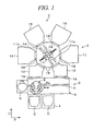
- FIG. 1 is a plane view illustrating a schematic configuration of a solar cell manufacturing apparatus 1 in accordance with the present invention.
- the solar cell manufacturing apparatus 1 has, for example, a configuration in which a cassette station 2 for loading/unloading a plurality of solar cell substrates W in a cassette unit and a processing station 3 having various kinds of processing units for performing a single-substrate process on the substrate W are connected with each other as one body.
- the cassette station 2 includes, for example, a cassette mounting unit 4, a transfer chamber 5, and an alignment unit 6 for positioning the solar cell substrate W.
- cassettes C capable of accommodating a plurality of solar cell substrates W can be mounted side by side in an X direction (in a right and left direction in Fig. 1 ).
- the transfer chamber 5 is adjacent to the cassette mounting unit 4 in a positive Y direction (in an upper direction in Fig. 1 ).
- the alignment unit 6 is adjacent to the transfer chamber 5 in a negative X direction (in the left direction in Fig. 1 ).
- the substrate transfer device 8 installed in the transfer chamber 5 includes a multi-joint transfer arm 8a which is pivotable, extensible and contractible, and can transfer the solar cell substrate W with respect to the cassette C in the cassette mounting unit 4, the alignment unit 6 and load lock chambers 12 and 13 of the processing station 3 to be described later.
- a central transfer chamber 10 as a transfer unit capable of depressurizing its inside.
- a substrate transfer mechanism 11 Installed within the central transfer chamber 10 is a substrate transfer mechanism 11.
- the central transfer chamber 10 is formed in an approximately octagon shape when viewed from the top, for example, and is surrounded by and connected with the load lock chambers 12 and 13 and four, for example, processing units 14, 15, 16 and 17.
- the substrate transfer mechanism 11 includes two transfer arms 11a and 11b which are pivotable, extensible and contractible, and can transfer the solar cell substrate W with respect to the load lock chambers 12 and 13 and the processing units 14 to 17 surrounding the central transfer chamber 10.
- the load lock chambers 12 and 13 are disposed between the central transfer chamber 10 and the transfer chamber 5 of the cassette station 2 and connect the central transfer chamber 10 with the transfer chamber 5.
- the load lock chambers 12 and 13 can include a non-illustrated mounting unit for mounting the solar cell substrate W thereon and maintain its inside in a depressurized atmosphere.
- Each gate valve 18 is installed between the transfer chamber 5 and the respective load lock chambers 12 and 13, between the central transfer chamber 10 and the respective load lock chambers 12 and 13, and between the central transfer chamber 10 and the respective processing units 14 to 17.
- the processing unit 14 is a plasma processing apparatus for performing an oxidation process, a nitridation process or an oxynitriding process on the solar cell substrate W by generating plasma using a radial line slot antenna.
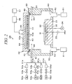
- the processing unit 14 includes, for example, as illustrated in Fig. 2 , a cylindrical processing chamber 30 having an open top surface and a bottom surface.
- the processing chamber 30 is made of, e.g., an aluminum alloy.
- the processing chamber 30 is grounded.
- Installed at a central portion of a bottom portion of the processing chamber 30 is a mounting table 31 for mounting, e.g., the solar cell substrate W thereon.
- an electrode plate 32 for example, is embedded, and the electrode plate 32 is connected with a DC power supply 33 installed at the outside of the processing chamber 30.
- An electrostatic force is generated on a surface of the mounting table 31 by the DC power supply 33, thereby electrostatically attracting the solar cell substrate W on the mounting table 31.
- a heater 35 for generating heat in response to a power feed from a heater power supply 34 is embedded in the mounting table 31, so that it is possible to heat the solar cell substrate W on the mounting table 31 to a predetermined temperature.
- a microwave transmission plate 41 installed at the opening in the top part of the processing chamber 30 is a microwave transmission plate 41 made of a dielectric material such as alumina (Al 2 O 3 ) or a quartz glass via a sealing member 40 such as an O-ring for securing airtightness.
- the inside of the processing chamber 30 is airtightly closed by the microwave transmission plate 41.
- a radial line slot antenna 42 providing a microwave for generating plasma.
- the radial line slot antenna 42 includes a substantially cylindrical case 42a having an open bottom surface on which there is formed a disc-shaped slot plate 43 having a plurality of slots therein.
- the slot plate 43 is a gold- or silver-plated copper or aluminum plate in which a plurality of microwave radiation holes 43a serving as slots are formed.
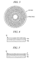
- the microwave radiation holes 43a adjacent to each other are formed in, e.g., a T-shape as illustrated in Fig. 3 and these T-shaped microwave radiation holes 43a are arranged in a concentric circular shape.
- a length of the microwave radiation hole 43a or a distance between them is determined based on a wavelength ⁇ of a microwave. For example, the distance between the microwave radiation holes 43a is set to be about (1/2) ⁇ or ⁇ .
- a shape of the microwave radiation holes 43a is not limited to a T-shape, so they can be formed in other shapes such as a circle, a circular arc or the like.
- an arrangement of the microwave radiation holes 43a is not limited to a concentric circular shape, so they can be arranged in a spiral shape, a grid pattern, a random manner, a radial shape, or the like.
- a wavelength shortening plate 44 installed at the top portion of the slot plate 43 is a wavelength shortening plate 44 made of a low-loss dielectric material as illustrated in Fig. 2 . Since a wavelength of the microwave is lengthened in a vacuum state, the wavelength shortening plate 44 shortens a wavelength of the microwave to control a generation state of plasma.
- the coaxial waveguide 45 is connected with a microwave oscillation apparatus 46 for generating a microwave of, e.g., 2.45 GHz.
- the microwave oscillation apparatus 46 is provided with a microwave oscillation control unit 47 for controlling ON ⁇ OFF or output of the microwave oscillation.
- a processing gas supply opening 50 which is connected with, e.g., a processing gas supply pipe 51 leading to the outside of the processing chamber 30.
- the processing gas supply pipe 51 is branched into plural, e.g., four branch pipes 51a, 51b, 51c and 51d, which are connected with gas supply sources 52a, 52b, 52c and 52d respectively.
- Installed at the respective branch pipes 51a to 51d are valves 53a, 53b, 53c and 53d and mass flow controllers 54a, 54b, 54c and 54d.
- sealed into, e.g., the gas supply source 52a is a rare gas, e.g., an Ar gas for generating plasma
- sealed into the gas supply source 52b is an oxygen (O 2 ) gas
- sealed into the gas supply source 52c is a dinitrogen monoxide (N 2 O) gas
- sealed into the gas supply source 52d is a hydrogen (H 2 ) gas.
- the number of the gas supply sources and gas species can be appropriately changed depending on kinds of the processing gases.
- exhaust openings 60 for exhausting an internal atmosphere of the processing chamber 30.
- the exhaust openings 60 are connected with gas exhaust units 61 such as a turbo-molecular pump via exhaust pipes 62.
- gas exhaust units 61 such as a turbo-molecular pump
- exhaust pipes 62 By the exhaustion through the exhaust openings 60, the inside of the processing chamber 30 can be depressurized to a predetermined pressure.
- a light absorption layer of a p-n junction including a polycrystalline silicon substrate Sp serving as a p-type layer and a polycrystalline silicon layer Sn serving as a n-type layer formed thereon.
- a passivation film is formed on a surface of the polycrystalline silicon layer Sn.
- each one of the solar cell substrates W is unloaded from the cassette C of the cassette station 2 by the substrate transfer device 8 illustrated in Fig. 1 and then is transferred to the alignment unit 6.
- the solar cell substrate W is position-adjusted by the alignment unit 6; transferred to the load lock chamber 12 by the substrate transfer device 8; and then transferred to, e.g., the processing unit 14 by the substrate transfer mechanism 11 via the central transfer chamber 10.
- the inside of the central transfer chamber 10 is maintained in a vacuum state and thus the solar cell substrate W passing through the inside of the central transfer chamber 10 is transferred in a vacuum state.
- the solar cell substrate W transferred to the processing unit 14 is attracted onto and held by the mounting table 31 as illustrated in Fig. 2 . Then, the solar cell substrate W is heated by the heater 35 to a temperature ranging from about 200°C to about 600°C, for example, 350°C. Subsequently, the inside of the processing chamber 30 is controlled to a pressure ranging from about 50 mTorr (6.67 Pa) to about 5 Torr (6. 67 ⁇ 10 2 Pa), for example, 100 mTorr (13.3 Pa), and then a gas mixture of an argon gas and an oxygen gas is introduced to the inside of the processing chamber 30 from the gas supply opening 50.
- a microwave is introduced to the inside of the processing chamber 30 from the radial line slot antenna 42.
- the processing gas in the processing chamber 30 is excited and plasma is generated within the processing chamber 30.
- the microwave passes through the slot plate 43 and forms a surface wave by which high density plasma is generated right under the microwave transmission plate 41.
- a sheath potential between a plasma generation space within the processing chamber 30 and a surface of the solar cell substrate W is maintained at 10 eV or less.
- a surface layer of the polycrystalline silicon layer Sn is oxidized by an action of the plasma containing oxygen atoms. Accordingly, as illustrated in Fig. 5 , formed on a surface of the polycrystalline silicon layer Sn is a passivation film A made of a silicon oxide film.
- the microwave or the processing gas is not any longer supplied and the process for forming the passivation film is ended.
- the solar cell substrate W is unloaded from the processing unit 14 by the substrate transfer mechanism 11 and transferred to the load lock chamber 13 via the central transfer chamber 10. Subsequently, the solar cell substrate W is returned to the cassette C by the substrate transfer device 8 and a series of processes is ended.
- the passivation film A is formed by using the plasma oxidation process, the polycrystalline silicon layer Sn and the passivation film A have a smooth and continuous interface therebetween without a grain boundary in comparison with a case using a conventional CVD process.
- crystal defects in the vicinity of the interface between the polycrystalline silicon layer Sn and the passivation film A decrease, so that energy carriers are rarely annihilated, whereby it is possible to manufacture a solar cell having a higher energy conversion efficiency in comparison with a conventional one.
- Fig. 6 illustrates a photoelectric conversion efficiency of a solar cell for each method for forming a passivation film. A photoelectric conversion efficiency is highly improved in a case using the plasma oxidation process as stated in the present embodiment as compared to a case using the conventional CVD process.
- a sheath potential (ion energy) on the surface of the solar cell substrate W and a crystal defect of the polycrystalline silicon layer Sn during a plasma processing it is found that a density of crystal defects decreases extremely below or equal to 2 ⁇ 10 +11 (1/cm 2 ) when a sheath potential is equal to or less than 10 eV as illustrated in Fig. 7 .
- the plasma processing is performed at a low ion energy having a sheath potential equal to or less than 10 eV, so that it is possible to reduce the crystal defects of the polycrystalline silicon layer Sn and manufacture a solar cell having a high photoelectric conversion efficiency.
- the plasma is concentrated right under the microwave transmission plate 41, so that the sheath potential of the surface of the solar cell substrate W can be kept stably low.
- a plasma processing is performed at a temperature less than 200°C, it is found that water or an organic material adhered to the surface of the polycrystalline silicon layer Sn is introduced into the film. Further, when a plasma processing is performed at a temperature higher than a 600°C, the polycrystalline silicon layer Sn is crystallized again. In the present embodiment, the plasma processing is performed at a temperature ranging from about 200°C to about 600°C, so that it is possible to form a passivation film A of a good quality containing little impurities therein.
- a plasma ion energy Ee or a plasma electron temperature Te can be reduced by increasing an internal pressure of the processing chamber 30 during the plasma processing.
- the polycrystalline silicon layer Sn can be oxidized at a low ion energy by setting the internal pressure of the processing chamber 30 to be equal to or more than 50 mTorr (6.67 Pa) during the processing.
- the crystal defects of the polycrystalline silicon layer Sn can be reduced and thus the solar cell having a high photoelectric conversion efficiency can be manufactured.
- the internal pressure of the processing chamber 30 is set too high during the processing, the ion energy is too much decreased and thus a rate of plasma oxidation decreases remarkably.
- the oxygen gas and the argon gas have been supplied as the processing gas
- a nitrogen (N 2 ) gas or an ammonia (NH 3 ) gas may be added to the processing gas, or a N 2 O gas, instead of the oxygen gas, may be used as the processing gas.
- the nitrogen atoms are introduced to the interface of the polycrystalline silicon layer Sn, the nitrogen atoms react selectively on the crystal defects formed in the interface between the polycrystalline silicon layer Sn and the passivation film A, which is an oxide film, and thus the nitrogen atoms restore the crystal defects. As a result, a final amount of the crystal defects decreases, so that it is possible to improve a photoelectric conversion efficiency of the solar cell. Further, it is found that when the nitrogen atom content ratio is more than 5 atomic% as illustrated in Fig. 9 , which means that the nitrogen atoms are oversupplied, the crystal defects in the interface of the polycrystalline silicon layer Sn increase, on the contrary. Accordingly, the crystal defects can be appropriately restored by the nitrogen atoms by maintaining the nitrogen atom content ratio to be equal to or less than 5 atomic%.
- the passivation film A has been formed by performing an oxidation process on the polycrystalline silicon layer Sn
- a N 2 O gas may be supplied instead of the oxygen gas to the processing unit 14.
- the microwave for generating plasma has been continuously supplied during the processing, it may be also possible to supply it intermittently in a pulse shape having a predetermined period.
- the microwave oscillation apparatus 46 generates a microwave formed in a pulse shape having a predetermined period under control of the microwave oscillation control unit 47 and the radial line slot antenna 42 supplies the pulse-shaped microwave into the processing chamber 30.
- the microwave is supplied such that a pulse frequency is about 50 kHz and a duty ratio (ratio of ON time to total ON ⁇ OFF time) is about 50%. As illustrated in Fig.
- a plasma ion energy is smaller in case that a pulse-shaped microwave (pulse wave) is supplied as compared to a case that a continuous microwave (continuous wave) is supplied. Therefore, it is possible to reduce the defects in the interface between the polycrystalline silicon layer Sn and the passivation film A by supplying the pulse-shaped microwave and to manufacture a solar cell having a high photoelectric conversion efficiency.
- the pulse frequency is about 50 kHz and the duty ratio is about 50%, it is found that as long as a pulse frequency is in a range from about 10 kHz to about 1 MHz and a duty ratio is in a range from about 20% to about 80%, it has an effect of reduction in crystal defects in comparison with the continuous wave.
- the passivation film A has been formed on the surface layer of the polycrystalline silicon layer Sn by, e.g., the plasma oxidation process, it may be also possible to deposit an additional passivation film on a top surface of the passivation film A by the CVD process.
- the solar cell manufacturing apparatus 1 includes other processing units 70 and 71 for performing the CVD process.
- the other processing units 70 and 71 instead of the above-stated processing units 16 and 17, are connected with the central transfer chamber 10.
- the other processing unit 70 is a plasma CVD apparatus for forming a film on a solar cell substrate W by generating plasma using a radial line slot antenna.
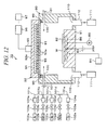
- the configuration of the other processing unit 70 is the same as that of the above-stated processing unit 14 except for that it is connected with a high frequency power supply so as to apply a bias power onto, e.g., a mounting table and it uses a different processing gas. That is, the other processing unit 70 includes a cylindrical processing chamber 80 having an open top surface and a bottom surface, and on a bottom portion of the processing chamber 80, there is installed a mounting table 81 as shown in Fig. 12 .
- the mounting table 81 Embedded in the mounting table 81 is an electrode plate 82 which is connected with a DC power supply 83. Further, the mounting table 81 is connected with a high frequency power supply 84 for applying a bias power onto, e.g., the solar cell substrate W. A heater 86 for generating heat in response to a power feed from a heater power supply 85 is embedded in the mounting table 81, so that the solar cell substrate W on the mounting table 81 can be heated to a predetermined temperature.
- a microwave transmission plate 91 Installed at the opening in the top part of the processing chamber 80 is a microwave transmission plate 91 via, e.g., a sealing member 90.
- the inside of the processing chamber 80 is airtightly closed by the microwave transmission plate 91.
- Installed at the top portion of the microwave transmission plate 91 is a radial line slot antenna 92.
- the radial line slot antenna 92 includes a substantially cylindrical case 92a having an open bottom surface on which a disc-shaped slot plate 93 is installed.
- the slot plate 93 has a plurality of microwave radiation holes 93a serving as slots.
- the microwave radiation holes 93a adjacent to each other are formed in, e.g., a T-shape as illustrated in Fig. 3 and these T-shaped microwave radiation holes 93a are arranged in a concentric circular shape.
- a length of the microwave radiation hole 93a or a distance between them is determined according to a wavelength ⁇ of a microwave.
- the distance between the microwave radiation holes 93a is set to be about (1/2) ⁇ or ⁇ .
- a wavelength shortening plate 94 installed at the top portion of the slot plate 93 is a wavelength shortening plate 94 made of a low-loss dielectric material as illustrated in Fig. 12 .
- the coaxial waveguide 95 is connected with a microwave oscillation apparatus 96 for generating a microwave of, e.g., 2.45 GHz.
- the microwave oscillation apparatus 96 is provided with a microwave oscillation control unit 97 for controlling ON ⁇ OFF or output of the microwave oscillation.
- a processing gas supply opening 100 which is connected with, e.g., a processing gas supply pipe 101 leading to the outside of the processing chamber 80.
- the processing gas supply pipe 101 is branched into plural, e.g., five branch pipes 101a, 101b, 101c, 101d and 101e, which are connected with gas supply sources 102a, 102b, 102c, 102d and 102e respectively.
- Installed at the respective branch pipes 101a to 101e are valves 103a, 103b, 103c, 103d and 103e and mass flow controllers 104a, 104b, 104c, 104d and 104e.
- the gas supply source 102a sealed into, e.g., the gas supply source 102a is a rare gas, e.g., an Ar gas, and sealed into the gas supply source 102b is a silane (SiH 4 ) gas. Further, sealed into the gas supply sources 102c, 102d and 102e are a nitrogen (N 2 ) gas, an ammonia (NH 3 ) gas and a hydrogen (H 2 ) gas respectively.
- N 2 nitrogen
- NH 3 ammonia
- H 2 hydrogen
- exhaust openings 110 installed at both sides of the mounting table 81 on the bottom portion of the processing chamber 80 are exhaust openings 110 which are connected with gas exhaust units 111 such as a turbo-molecular pump via exhaust pipes 112.
- gas exhaust units 111 such as a turbo-molecular pump
- exhaust pipes 112. By the exhaustion through the exhaust openings 110, the inside of the processing chamber 80 can be depressurized to a predetermined pressure.
- the solar cell substrate W having the polycrystalline silicon substrate Sp and the polycrystalline silicon layer Sn formed thereon as illustrated in Fig. 4 is transferred to the alignment unit 6 from the cassette C by the substrate transfer device 8 in the same manner as the above-described embodiment. Thereafter, the solar cell substrate W is transferred to the load lock chamber 12 by the substrate transfer device 8 and transferred to, e.g., the processing unit 14 by the substrate transfer mechanism 11 via the central transfer chamber 10.
- a surface layer of the polycrystalline silicon layer Sn is oxidized by the plasma processing in the same manner as the aforementioned embodiment. Accordingly, as shown in Fig. 13 , a passivation film Al is formed on the surface of the polycrystalline silicon layer Sn.
- the solar cell substrate W is unloaded from the processing unit 14 by the substrate transfer mechanism 11 and transferred to, e.g., the other processing unit 70 via the central transfer chamber 10. At this time, the solar cell substrate W is transferred in a vacuum state in order not to be exposed to the air.
- the solar cell substrate W transferred to the other processing unit 70 is attracted onto and held by the mounting table 81 as illustrated in Fig. 12 . Then, the solar cell substrate W is heated by the heater 86 to a temperature ranging from about 200°C to about 600°C. Subsequently, the inside of the processing chamber 80 is controlled to a pressure ranging from about 5 mTorr to about 5 Torr, and then a gas mixture of an argon gas, a silane gas and a nitrogen gas is introduced to the inside of the processing chamber 80 from the gas supply opening 100.
- a microwave is introduced to the inside of the processing chamber 80 from the radial line slot antenna 92.
- the gas in the processing chamber 80 is excited into plasma within the processing chamber 80.
- the microwave passes through the slot plate 93 and forms a surface wave by which high density plasma is generated right under the microwave transmission plate 91.
- the high frequency power supply 84 applies a bias power of 20V or more onto the solar cell substrate W on the mounting table 81.
- a silicon nitride film is deposited on a surface of a first passivation film Al by an action of plasma, thereby forming a second passivation film A2 as illustrated in Fig. 14 .
- a passivation film Al + A2 having a predetermined thickness of, e.g., about 10 nm or more on the whole.
- the microwave or the processing gas is not any longer supplied and the process for forming the passivation film is ended.
- the solar cell substrate W is unloaded from the other processing unit 70 by the substrate transfer mechanism 11 and then transferred to the load lock chamber 13 via the central transfer chamber 10. Then, the solar cell substrate W is returned to the cassette C by the substrate transfer device 8 and a series of processes is ended.
- the second passivation film A2 on the first passivation film Al by the CVD process, even if the passivation film having a satisfactory thickness can not be obtained by performing the plasma oxidation process only, it is possible to form a passivation film having a sufficient thickness by the subsequent CVD process. As a result, the passivation film can fully function as, e.g., an anti-reflection film. Furthermore, the passivation film having a satisfactory strength may be obtained. Moreover, in this embodiment, by forming the silicon nitride film having a higher reflectivity on the silicon oxide film serving as the first passivation film A1, an anti-reflection function of the passivation film can be more improved.
- the silicon nitride film formed by the CVD process has a higher refractive index than the silicon oxide film, it becomes easy to confine a light in the passivation film by the combination of the plasma oxidation process and the CVD process and thus the photoelectric conversion efficiency is improved.
- the processing unit 14 By connecting the processing unit 14 with the other processing unit 70 via the central transfer chamber 10 and transferring the solar cell substrate W from the processing unit 14 to the other processing unit 70 in a vacuum state, it is possible to prevent the film quality from being deteriorated due to, for example, water adhered thereonto when the solar cell substrate W is exposed to the air. Furthermore, it may be possible to perform both the process for forming the first passivation film A1 and the process for forming the second passivation film A2 within the same processing chamber, and for example, within the processing chamber 80 of the other processing unit 70, it may be possible to form the first passivation film Al by performing the above-stated plasma oxidation process and then form the second passivation film A2 by performing the plasma CVD process.
- the first passivation film Al is an oxide film
- an oxygen gas in addition to a nitrogen gas is introduced as a processing gas for the CVD process and a ratio of a nitrogen to an oxygen increases gradually when introducing the processing gas, whereby it may be possible to gradually increase a content ratio of nitrogen atoms in the second passivation film A2 in a deposition direction.
- a small amount of the nitrogen gas as compared to the oxygen gas is introduced in the beginning; then the introduced amount of the nitrogen gas is increased as the introduced amount of the oxygen gas is decreased; and finally, only the nitrogen gas is introduced thereto.
- a film composition of the second passivation film A2 is gradually changed from the silicon oxide film to the silicon nitride film, so that a film composition of the first passivation film A1, which is the silicon oxide film, becomes generally continuous with that of the second passivation film A2. Accordingly, a grain boundary in the passivation film decreases, so that crystal defects can be reduced. Furthermore, this embodiment can be applied to a case in which the first passivation film Al is an oxynitride film.
- the SiH 4 (silane) gas is used as the processing gas for the CVD process
- other gases such as a Si 2 H 6 (disilane) gas instead.
- the process for forming the first passivation film Al on the polycrystalline silicon layer Sn and the CVD process for forming the second passivation film A2 which are described in the foregoing embodiment, it may be possible to add a hydrogen gas to the processing gas.
- the hydrogen atoms react selectively on the crystal defects formed in the passivation film and in the interface between the silicon layer and the passivation film, the crystal defects can be restored. As a result, a solar cell having a much higher photoelectric conversion efficiency can be fabricated.
- processing units 14 to 17 and the other processing units 70 and 71 described in the foregoing embodiment include the above-stated radial line slot antenna, they may include a slot antenna having a different configuration.
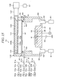
- the processing unit 14 includes a parallel plate waveguide slot antenna (hereinafter, referred to as "parallel plate antenna") 130 at the top portion of the microwave transmission plate 41 as illustrated in Fig. 15 .
- the parallel plate antenna 130 is an antenna in which slots are formed in one of two plates constituting a parallel plate waveguide.
- the parallel plate antenna 130 includes a first waveguide plate 130a having a square-shape at a lower side thereof and a second waveguide plate 130b having a square-shape at a upper side thereof, which are disposed parallel to each other.
- a parallel plate waveguide 131 is formed at a gap between the first and the second waveguide plates 130a and 130b.
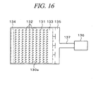
- a plurality of microwave radiation holes 132 serving as slots is formed in the first waveguide plate 130a.
- the microwave radiation holes 132 adjacent to each other are formed in, e.g., a T-shape as illustrated in Fig.
- T-shaped microwave radiation holes 132 are arranged lengthwise and breadthwise in a regular line.
- a length of the microwave radiation holes 132 or an arrangement distance between them is determined according to a wavelength ⁇ of a microwave in the parallel plate waveguide 131.
- the distance between the microwave radiation holes 132 is set to be a natural number multiple of ⁇ .
- a shape of the microwave radiation holes 132 is not limited to a T-shape, so they can be formed in other shapes such as circle, a circular arc or the like.
- arrangement of the microwave radiation holes 132 is not limited to a lengthwise and breadthwise arrangement, so they can be arranged in a concentric circle shape, a spiral shape, a random manner, a radial shape, or the like.
- a wavelength shortening member 133 installed within the parallel plate waveguide 131 is a wavelength shortening member 133 made of a dielectric material.
- a wavelength of a microwave introduced to the parallel plate waveguide 131 can be shortened by the wavelength shortening member 133, whereby it is possible to control a generation state of plasma.
- a microwave absorption member 134 is formed at one end portion within the parallel plate waveguide 131.
- a microwave distribution unit 135 for distributing the introduced microwave.
- the microwave distribution unit 135 is connected with a waveguide 137 which is connected with a microwave oscillation apparatus 136 for generating a microwave of, e.g., 2.45 GHz. Since a configuration of the other parts of the processing unit 14 is the same as that of the processing unit 14 described in the foregoing embodiment, so that they are assigned the same reference numerals and a detailed explanation thereof is omitted.
- the microwave generated from the microwave oscillation apparatus 136 is introduced to the parallel plate waveguide 131 of the parallel plate antenna 130; passes through the microwave radiation hole 132 of the first waveguide plate 130a; and then is introduced into the processing chamber 30 via the microwave transmission plate 41. Accordingly, formed within the processing chamber 30 is a surface wave of the microwave by which high density plasma is generated right under the microwave transmission plate 41.
- processing units 15, 16 and 17 and the other processing units 70 and 71 may include the parallel plate antenna 130 as well.
- the present embodiment provides an example of forming a passivation film on a polycrystalline silicon layer, but the present invention can be applied to a case of forming a passivation film on a monocrystalline silicon layer, an amorphous silicon layer, or a silicon layer in which polycrystalline silicon and amorphous silicon co-exist.
- the present invention is useful in manufacturing a solar cell having a high energy conversion efficiency.
Landscapes
- Chemical & Material Sciences (AREA)
- Engineering & Computer Science (AREA)
- Mechanical Engineering (AREA)
- Chemical Kinetics & Catalysis (AREA)
- General Chemical & Material Sciences (AREA)
- Materials Engineering (AREA)
- Metallurgy (AREA)
- Organic Chemistry (AREA)
- Inorganic Chemistry (AREA)
- Physics & Mathematics (AREA)
- Plasma & Fusion (AREA)
- Photovoltaic Devices (AREA)
- Chemical Vapour Deposition (AREA)
- Plasma Technology (AREA)
- Formation Of Insulating Films (AREA)
Abstract
Description
- The present invention relates to a manufacturing method of a solar cell and a manufacturing apparatus of a solar cell.
- For example, in a crystalline silicon-based solar cell, a p-n junction is formed on a silicon layer serving as a light absorption layer, and formed on a surface of the silicon layer is a passivation film used for protecting a device or for preventing a light incident on the light absorption layer from being reflected to the outside.
- In a conventional way, a passivation film is formed by performing a thermal oxidation process on a surface of a silicon layer. However, if the surface of the silicon layer is thermally oxidized at a high temperature in such way, defects such as a multiple number of holes are generated in an interface between the passivation film formed by the thermal oxidation process and an underlying silicon layer. For this reason, those defects function as a main cause for recombination of carriers such as electrons, so that the carriers are recombined and annihilated, whereby an energy conversion efficiency of a finally fabricated solar cell is lowered. In order to solve this problem, it has been considered to form a silicon nitride film serving as a passivation film on a surface of a silicon layer by a plasma CVD process instead of the thermal oxidation process (see Patent Document 1). Since the silicon nitride film formed by the plasma CVD process is hardly affected by a grain boundary of crystalline silicon, it is possible to suppress an annihilation of the carriers.
Patent Document 1: Japanese Patent Laid-open Publication No.2005-159171 - However, when a passivation film is formed by a plasma CVD process as stated above, a silicon nitride film is newly deposited on a silicon layer, so that an interface between the silicon layer and the passivation film becomes discontinuous. For this reason, many crystal defects still exist in the vicinity of the interface between the silicon layer and the passivation film, thereby causing the annihilation of the carriers. Accordingly, a sufficiently high energy conversion efficiency can not be attained even by the plasma CVD process.
- In view of the foregoing, there is provided a manufacturing method and a manufacturing apparatus of a solar cell capable of attaining a high energy conversion efficiency.
- In accordance with one aspect of the present invention, there is provided a solar cell manufacturing method including: forming a passivation film on a surface layer of a silicon layer by performing an oxidation process, a nitridation process or an oxynitriding process on the surface layer of the silicon layer by using plasma.
- In accordance with present invention, it is possible to manufacture a solar cell having a high energy conversion efficiency by forming a passivation film through a plasma processing performed on a surface layer of a silicon layer.
- In the solar cell manufacturing method, the passivation film may be formed by using plasma having a sheath potential of about 10 eV or less. Herein, the sheath potential implies a potential difference between a space, in which plasma is generated, and a silicon layer.
- Further, the passivation film may be formed at a pressure ranging from about 6.67 Pa to about 6.67 × 10² Pa.
- Furthermore, the passivation film may be formed at a temperature ranging from about 200°C to about 600°C.
- The plasma may be surface wave plasma excited by a microwave.
- The microwave for generating the plasma may be supplied through a slot antenna.
- The microwave for generating the plasma may be supplied intermittently in a pulse shape having a predetermined period.
- In case of performing the oxidation process on a surface layer of a polycrystalline silicon layer, a processing gas containing nitrogen may be introduced into a processing chamber such that a nitrogen atom content ratio in an interface between the polycrystalline silicon layer and the passivation film is equal to or less than about 5 atomic%.
- On the passivation film formed on the silicon layer, a passivation film may be further formed by depositing an oxide film, a nitride film or an oxynitride film by a CVD process.
- The passivation film may be formed by the CVD process using plasma.
- In the CVD process, a bias power may be applied onto a deposition layer of the passivation film.
- In at least one of the oxidation process, the nitridation process or the oxynitriding process performed on the surface layer of the silicon layer and the CVD process, a hydrogen gas may be added to a processing gas.
- The oxidation process, the nitridation process or the oxynitriding process performed on the surface layer of the silicon layer and the CVD process may be performed within a same processing chamber.
- The oxidation process, the nitridation process or the oxynitriding process performed on the surface layer of the silicon layer and the CVD process may be performed in different processing chambers and a solar cell substrate may be transferred between the processing chambers in a vacuum state.
- In case of forming the passivation film by performing the oxynitriding process on the surface layer of the silicon layer, a processing gas containing oxygen and nitrogen may be introduced into a processing chamber during the CVD process and a ratio of the nitrogen to the oxygen in the introduced processing gas may be gradually increased such that a content ratio of nitrogen atoms in the passivation film is gradually increased in a deposition direction.
- In accordance with another aspect of the present invention, there is provided a solar cell manufacturing apparatus including: a processing unit for forming a passivation film on a surface layer of a silicon layer by performing an oxidation process, a nitridation process or an oxynitriding process on the surface layer of the silicon layer by using plasma.
- The processing unit may form the passivation film by using plasma having a sheath potential of about 10 eV or less.
- The processing unit may form the passivation film at a pressure ranging from about 6.67 Pa to about 6.67 × 10² Pa.
- The processing unit may form the passivation film at a temperature ranging from about 200°C to about 600°C.
- The plasma may be surface wave plasma excited by a microwave.
- The processing unit may include a slot antenna for supplying the microwave.
- The microwave for generating the plasma may be supplied intermittently in a pulse shape having a predetermined period.
- In case of performing the oxidation process on a surface layer of a polycrystalline silicon layer, a processing gas containing nitrogen may be introduced into a processing chamber such that a nitrogen atom content ratio in an interface between the polycrystalline silicon layer and the passivation film is equal to or less than about 5 atomic%.
- The solar cell manufacturing apparatus may include other processing unit for further forming a passivation film on the passivation film formed on the silicon layer by depositing an oxide film, a nitride film or an oxynitride film by a CVD process.
- The other processing unit may form the passivation film by the CVD process using plasma.
- The other processing unit may include a power supply for applying a bias power onto a deposition layer of the passivation film.
- In at least one of the oxidation process, the nitridation process or the oxynitriding process performed on the surface layer of the silicon layer in the processing unit and the CVD process performed in the other processing unit, a hydrogen gas may be added to a processing gas.
- The processing unit and the other processing unit may be connected with each other via a transfer unit for transferring a solar cell substrate in a vacuum state.
- In case of forming the passivation film by performing the oxynitriding process on the surface layer of the silicon layer in the processing unit, a processing gas containing oxygen and nitrogen may be introduced into a processing chamber during the CVD process performed in the other processing unit and a ratio of the nitrogen to the oxygen in the introduced processing gas may be gradually increased such that a content ratio of nitrogen atoms in the passivation film is gradually increased in a deposition direction.
- In accordance with the present invention, it is possible to manufacture a solar cell having a high energy conversion efficiency.
-
-
Fig. 1 is a plane view illustrating a schematic configuration of a manufacturing apparatus of a solar cell in accordance with the present embodiment; -
Fig. 2 is a schematic view of a configuration of a processing unit; -
Fig. 3 is a plane view of a configuration of a slot plate; -
Fig. 4 is a diagram illustrating a longitudinal cross section of a solar cell substrate in which a polycrystalline silicon layer is formed on a polycrystalline silicon substrate; -
Fig. 5 is a diagram illustrating a longitudinal cross section of a solar cell substrate in which a passivation film is formed; -
Fig. 6 is a graph showing a photoelectric conversion efficiency of a solar cell for each method of forming a passivation film; -
Fig. 7 is a graph illustrating a relationship between a sheath potential and a crystal defect density during a plasma processing; -
Fig. 8 is a graph illustrating a relationship of an ion energy and an electron temperature with respect to a pressure during a plasma processing; -
Fig. 9 is a graph showing a relationship between a nitride atom content ratio and a crystal defect density in an interface between a polycrystalline silicon layer and a passivation film; -
Fig. 10 is a graph showing a difference in ion energies between a continuous microwave and a pulse-shaped microwave; -
Fig. 11 is a plane view illustrating a schematic configuration of a manufacturing apparatus of a solar cell in accordance with another embodiment; -
Fig. 12 is a schematic view of a configuration of another processing unit; -
Fig. 13 is a diagram illustrating a longitudinal cross section of a solar cell substrate in which a first passivation film is formed; -
Fig. 14 is a diagram illustrating a longitudinal cross section of a solar cell substrate in which a second passivation film is formed; -
Fig. 15 is a schematic view of another configuration of a processing unit; and -
Fig. 16 is a plane view illustrating an internal configuration of a parallel plate waveguide. -
- 1 : Manufacturing apparatus of a solar cell
- 14 : Processing unit
- 42 : Radial line slot antenna
- Sp : Polycrystalline silicon substrate
- Sn : Polycrystalline silicon layer
- A : Passivation film
- W : Solar cell substrate
- Hereinafter, an embodiment of the present invention will be described in detail with reference to the accompanying drawings.
Fig. 1 is a plane view illustrating a schematic configuration of a solarcell manufacturing apparatus 1 in accordance with the present invention. - As illustrated in
Fig. 1 , the solarcell manufacturing apparatus 1 has, for example, a configuration in which acassette station 2 for loading/unloading a plurality of solar cell substrates W in a cassette unit and aprocessing station 3 having various kinds of processing units for performing a single-substrate process on the substrate W are connected with each other as one body. - The
cassette station 2 includes, for example, acassette mounting unit 4, atransfer chamber 5, and analignment unit 6 for positioning the solar cell substrate W. In thecassette mounting unit 4, cassettes C capable of accommodating a plurality of solar cell substrates W can be mounted side by side in an X direction (in a right and left direction inFig. 1 ). Thetransfer chamber 5 is adjacent to thecassette mounting unit 4 in a positive Y direction (in an upper direction inFig. 1 ). In thetransfer chamber 5, there are installed atransfer rail 7 extending, for example, in the X direction and asubstrate transfer device 8 moving along thetransfer rail 7. Thealignment unit 6 is adjacent to thetransfer chamber 5 in a negative X direction (in the left direction inFig. 1 ). Thesubstrate transfer device 8 installed in thetransfer chamber 5 includes amulti-joint transfer arm 8a which is pivotable, extensible and contractible, and can transfer the solar cell substrate W with respect to the cassette C in thecassette mounting unit 4, thealignment unit 6 and loadlock chambers processing station 3 to be described later. - At a central portion of the
processing station 3, there is installed acentral transfer chamber 10 as a transfer unit capable of depressurizing its inside. Installed within thecentral transfer chamber 10 is asubstrate transfer mechanism 11. Thecentral transfer chamber 10 is formed in an approximately octagon shape when viewed from the top, for example, and is surrounded by and connected with theload lock chambers processing units substrate transfer mechanism 11 includes twotransfer arms load lock chambers processing units 14 to 17 surrounding thecentral transfer chamber 10. - The
load lock chambers central transfer chamber 10 and thetransfer chamber 5 of thecassette station 2 and connect thecentral transfer chamber 10 with thetransfer chamber 5. Theload lock chambers - Each
gate valve 18 is installed between thetransfer chamber 5 and the respectiveload lock chambers central transfer chamber 10 and the respectiveload lock chambers central transfer chamber 10 and therespective processing units 14 to 17. - The
processing unit 14 is a plasma processing apparatus for performing an oxidation process, a nitridation process or an oxynitriding process on the solar cell substrate W by generating plasma using a radial line slot antenna. - The
processing unit 14 includes, for example, as illustrated inFig. 2 , acylindrical processing chamber 30 having an open top surface and a bottom surface. Theprocessing chamber 30 is made of, e.g., an aluminum alloy. Theprocessing chamber 30 is grounded. Installed at a central portion of a bottom portion of theprocessing chamber 30 is a mounting table 31 for mounting, e.g., the solar cell substrate W thereon. - In the mounting table 31, an
electrode plate 32, for example, is embedded, and theelectrode plate 32 is connected with aDC power supply 33 installed at the outside of theprocessing chamber 30. An electrostatic force is generated on a surface of the mounting table 31 by theDC power supply 33, thereby electrostatically attracting the solar cell substrate W on the mounting table 31. Aheater 35 for generating heat in response to a power feed from a heater power supply 34 is embedded in the mounting table 31, so that it is possible to heat the solar cell substrate W on the mounting table 31 to a predetermined temperature. - Installed at the opening in the top part of the
processing chamber 30 is amicrowave transmission plate 41 made of a dielectric material such as alumina (Al2O3) or a quartz glass via a sealingmember 40 such as an O-ring for securing airtightness. The inside of theprocessing chamber 30 is airtightly closed by themicrowave transmission plate 41. Installed at the top portion of themicrowave transmission plate 41 is a radialline slot antenna 42 providing a microwave for generating plasma. - The radial
line slot antenna 42 includes a substantiallycylindrical case 42a having an open bottom surface on which there is formed a disc-shapedslot plate 43 having a plurality of slots therein. Theslot plate 43 is a gold- or silver-plated copper or aluminum plate in which a plurality ofmicrowave radiation holes 43a serving as slots are formed. Themicrowave radiation holes 43a adjacent to each other are formed in, e.g., a T-shape as illustrated inFig. 3 and these T-shapedmicrowave radiation holes 43a are arranged in a concentric circular shape. A length of themicrowave radiation hole 43a or a distance between them is determined based on a wavelength λ of a microwave. For example, the distance between themicrowave radiation holes 43a is set to be about (1/2)λ or λ. Further, a shape of themicrowave radiation holes 43a is not limited to a T-shape, so they can be formed in other shapes such as a circle, a circular arc or the like. Furthermore, an arrangement of themicrowave radiation holes 43a is not limited to a concentric circular shape, so they can be arranged in a spiral shape, a grid pattern, a random manner, a radial shape, or the like. - Installed at the top portion of the
slot plate 43 is awavelength shortening plate 44 made of a low-loss dielectric material as illustrated inFig. 2 . Since a wavelength of the microwave is lengthened in a vacuum state, thewavelength shortening plate 44 shortens a wavelength of the microwave to control a generation state of plasma. - Formed at a central portion of the
case 42a of the radialline slot antenna 42 is an opening which is connected with acoaxial waveguide 45. Thecoaxial waveguide 45 is connected with amicrowave oscillation apparatus 46 for generating a microwave of, e.g., 2.45 GHz. Themicrowave oscillation apparatus 46 is provided with a microwaveoscillation control unit 47 for controlling ON·OFF or output of the microwave oscillation. - For example, in a sidewall of the
processing chamber 30, there is formed a processinggas supply opening 50 which is connected with, e.g., a processinggas supply pipe 51 leading to the outside of theprocessing chamber 30. The processinggas supply pipe 51 is branched into plural, e.g., fourbranch pipes gas supply sources respective branch pipes 51a to 51d arevalves mass flow controllers processing chamber 30 at a predetermined flow rate. In the present embodiment, sealed into, e.g., thegas supply source 52a is a rare gas, e.g., an Ar gas for generating plasma, and sealed into thegas supply source 52b is an oxygen (O2) gas. Further, sealed into thegas supply source 52c is a dinitrogen monoxide (N2O) gas, and sealed into thegas supply source 52d is a hydrogen (H2) gas. Furthermore, the number of the gas supply sources and gas species can be appropriately changed depending on kinds of the processing gases. - For example, installed at both sides of the mounting table 31 on the bottom portion of the
processing chamber 30 areexhaust openings 60 for exhausting an internal atmosphere of theprocessing chamber 30. Theexhaust openings 60 are connected withgas exhaust units 61 such as a turbo-molecular pump viaexhaust pipes 62. By the exhaustion through theexhaust openings 60, the inside of theprocessing chamber 30 can be depressurized to a predetermined pressure. - Since the configuration of the
processing units 15 to 17 are the same as that of the above-describedprocessing unit 14, an explanation thereof is omitted. - Hereinafter, there will be explained a process for forming a passivation film of a solar cell, which is performed in the above-stated solar
cell manufacturing apparatus 1. - In the present embodiment, for example, as illustrated in
Fig. 4 , formed on a solar cell substrate W is a light absorption layer of a p-n junction including a polycrystalline silicon substrate Sp serving as a p-type layer and a polycrystalline silicon layer Sn serving as a n-type layer formed thereon. A passivation film is formed on a surface of the polycrystalline silicon layer Sn. - In accordance with the process for forming the passivation film, each one of the solar cell substrates W is unloaded from the cassette C of the
cassette station 2 by thesubstrate transfer device 8 illustrated inFig. 1 and then is transferred to thealignment unit 6. The solar cell substrate W is position-adjusted by thealignment unit 6; transferred to theload lock chamber 12 by thesubstrate transfer device 8; and then transferred to, e.g., theprocessing unit 14 by thesubstrate transfer mechanism 11 via thecentral transfer chamber 10. At this time, the inside of thecentral transfer chamber 10 is maintained in a vacuum state and thus the solar cell substrate W passing through the inside of thecentral transfer chamber 10 is transferred in a vacuum state. - The solar cell substrate W transferred to the
processing unit 14 is attracted onto and held by the mounting table 31 as illustrated inFig. 2 . Then, the solar cell substrate W is heated by theheater 35 to a temperature ranging from about 200°C to about 600°C, for example, 350°C. Subsequently, the inside of theprocessing chamber 30 is controlled to a pressure ranging from about 50 mTorr (6.67 Pa) to about 5 Torr (6. 67 × 102 Pa), for example, 100 mTorr (13.3 Pa), and then a gas mixture of an argon gas and an oxygen gas is introduced to the inside of theprocessing chamber 30 from thegas supply opening 50. - Thereafter, a microwave is introduced to the inside of the
processing chamber 30 from the radialline slot antenna 42. By introduction of the microwave, the processing gas in theprocessing chamber 30 is excited and plasma is generated within theprocessing chamber 30. At this time, the microwave passes through theslot plate 43 and forms a surface wave by which high density plasma is generated right under themicrowave transmission plate 41. Further, a sheath potential between a plasma generation space within theprocessing chamber 30 and a surface of the solar cell substrate W is maintained at 10 eV or less. On the surface of the solar cell substrate W, a surface layer of the polycrystalline silicon layer Sn is oxidized by an action of the plasma containing oxygen atoms. Accordingly, as illustrated inFig. 5 , formed on a surface of the polycrystalline silicon layer Sn is a passivation film A made of a silicon oxide film. - When the passivation film A having a desired thickness is formed by performing a plasma oxidation process for a predetermined time, the microwave or the processing gas is not any longer supplied and the process for forming the passivation film is ended.
- Then, the solar cell substrate W is unloaded from the
processing unit 14 by thesubstrate transfer mechanism 11 and transferred to theload lock chamber 13 via thecentral transfer chamber 10. Subsequently, the solar cell substrate W is returned to the cassette C by thesubstrate transfer device 8 and a series of processes is ended. - In accordance with the above-stated embodiment, since the passivation film A is formed by using the plasma oxidation process, the polycrystalline silicon layer Sn and the passivation film A have a smooth and continuous interface therebetween without a grain boundary in comparison with a case using a conventional CVD process. As a result, crystal defects in the vicinity of the interface between the polycrystalline silicon layer Sn and the passivation film A decrease, so that energy carriers are rarely annihilated, whereby it is possible to manufacture a solar cell having a higher energy conversion efficiency in comparison with a conventional one.
Fig. 6 illustrates a photoelectric conversion efficiency of a solar cell for each method for forming a passivation film. A photoelectric conversion efficiency is highly improved in a case using the plasma oxidation process as stated in the present embodiment as compared to a case using the conventional CVD process. - In regard to a relationship between a sheath potential (ion energy) on the surface of the solar cell substrate W and a crystal defect of the polycrystalline silicon layer Sn during a plasma processing, it is found that a density of crystal defects decreases extremely below or equal to 2 × 10+11 (1/cm2) when a sheath potential is equal to or less than 10 eV as illustrated in
Fig. 7 . In the present embodiment, the plasma processing is performed at a low ion energy having a sheath potential equal to or less than 10 eV, so that it is possible to reduce the crystal defects of the polycrystalline silicon layer Sn and manufacture a solar cell having a high photoelectric conversion efficiency. - In particular, by using the radial
line slot antenna 42 as a microwave supply unit, the plasma is concentrated right under themicrowave transmission plate 41, so that the sheath potential of the surface of the solar cell substrate W can be kept stably low. - When a plasma processing is performed at a temperature less than 200°C, it is found that water or an organic material adhered to the surface of the polycrystalline silicon layer Sn is introduced into the film. Further, when a plasma processing is performed at a temperature higher than a 600°C, the polycrystalline silicon layer Sn is crystallized again. In the present embodiment, the plasma processing is performed at a temperature ranging from about 200°C to about 600°C, so that it is possible to form a passivation film A of a good quality containing little impurities therein.
- As illustrated in
Fig. 8 , it is found that a plasma ion energy Ee or a plasma electron temperature Te can be reduced by increasing an internal pressure of theprocessing chamber 30 during the plasma processing. As performed in the present embodiment, the polycrystalline silicon layer Sn can be oxidized at a low ion energy by setting the internal pressure of theprocessing chamber 30 to be equal to or more than 50 mTorr (6.67 Pa) during the processing. As a result, the crystal defects of the polycrystalline silicon layer Sn can be reduced and thus the solar cell having a high photoelectric conversion efficiency can be manufactured. However, if the internal pressure of theprocessing chamber 30 is set too high during the processing, the ion energy is too much decreased and thus a rate of plasma oxidation decreases remarkably. In accordance with the present embodiment, it is possible to avoid a remarkable decrease of the plasma oxidation rate by maintaining the internal pressure of theprocessing chamber 30 to be equal to or less than 5 Torr (6.67 × 10² Pa). - In the above-stated embodiment, although the oxygen gas and the argon gas have been supplied as the processing gas, it may be also possible to maintain a nitrogen atom content ratio in the interface between the polycrystalline silicon layer Sn and the passivation film A to be equal to or less than 5 atomic% by adding nitrogen to the processing gas. In order to add the nitrogen to the processing gas, a nitrogen (N2) gas or an ammonia (NH3) gas may be added to the processing gas, or a N2O gas, instead of the oxygen gas, may be used as the processing gas. In this case, since the nitrogen atoms are introduced to the interface of the polycrystalline silicon layer Sn, the nitrogen atoms react selectively on the crystal defects formed in the interface between the polycrystalline silicon layer Sn and the passivation film A, which is an oxide film, and thus the nitrogen atoms restore the crystal defects. As a result, a final amount of the crystal defects decreases, so that it is possible to improve a photoelectric conversion efficiency of the solar cell. Further, it is found that when the nitrogen atom content ratio is more than 5 atomic% as illustrated in
Fig. 9 , which means that the nitrogen atoms are oversupplied, the crystal defects in the interface of the polycrystalline silicon layer Sn increase, on the contrary. Accordingly, the crystal defects can be appropriately restored by the nitrogen atoms by maintaining the nitrogen atom content ratio to be equal to or less than 5 atomic%. - In the above-stated embodiment, though the passivation film A has been formed by performing an oxidation process on the polycrystalline silicon layer Sn, it may be also possible to form a passivation film by performing an oxynitriding process. In this case, a N2O gas may be supplied instead of the oxygen gas to the
processing unit 14. Even in this case, it is possible to manufacture a solar cell having a high photoelectric conversion efficiency as compared to a case using a conventional CVD process, as illustrated inFig. 6 . Furthermore, it may be also possible to form a passivation film by performing a nitridation process on the polycrystalline silicon film Sn by supplying the nitrogen gas instead of the oxygen gas. - In the above-stated embodiment, though the microwave for generating plasma has been continuously supplied during the processing, it may be also possible to supply it intermittently in a pulse shape having a predetermined period. In this case, for example, the
microwave oscillation apparatus 46 generates a microwave formed in a pulse shape having a predetermined period under control of the microwaveoscillation control unit 47 and the radialline slot antenna 42 supplies the pulse-shaped microwave into theprocessing chamber 30. For example, the microwave is supplied such that a pulse frequency is about 50 kHz and a duty ratio (ratio of ON time to total ON·OFF time) is about 50%. As illustrated inFig. 10 , it is found that a plasma ion energy is smaller in case that a pulse-shaped microwave (pulse wave) is supplied as compared to a case that a continuous microwave (continuous wave) is supplied. Therefore, it is possible to reduce the defects in the interface between the polycrystalline silicon layer Sn and the passivation film A by supplying the pulse-shaped microwave and to manufacture a solar cell having a high photoelectric conversion efficiency. Furthermore, in this example, though the pulse frequency is about 50 kHz and the duty ratio is about 50%, it is found that as long as a pulse frequency is in a range from about 10 kHz to about 1 MHz and a duty ratio is in a range from about 20% to about 80%, it has an effect of reduction in crystal defects in comparison with the continuous wave. - In the above-stated embodiment, though the passivation film A has been formed on the surface layer of the polycrystalline silicon layer Sn by, e.g., the plasma oxidation process, it may be also possible to deposit an additional passivation film on a top surface of the passivation film A by the CVD process.
-
Fig. 11 provides such an embodiment. The solarcell manufacturing apparatus 1 includesother processing units other processing units processing units central transfer chamber 10. - For example, the
other processing unit 70 is a plasma CVD apparatus for forming a film on a solar cell substrate W by generating plasma using a radial line slot antenna. - The configuration of the
other processing unit 70 is the same as that of the above-statedprocessing unit 14 except for that it is connected with a high frequency power supply so as to apply a bias power onto, e.g., a mounting table and it uses a different processing gas. That is, theother processing unit 70 includes acylindrical processing chamber 80 having an open top surface and a bottom surface, and on a bottom portion of theprocessing chamber 80, there is installed a mounting table 81 as shown inFig. 12 . - Embedded in the mounting table 81 is an
electrode plate 82 which is connected with aDC power supply 83. Further, the mounting table 81 is connected with a highfrequency power supply 84 for applying a bias power onto, e.g., the solar cell substrateW. A heater 86 for generating heat in response to a power feed from a heater power supply 85 is embedded in the mounting table 81, so that the solar cell substrate W on the mounting table 81 can be heated to a predetermined temperature. - Installed at the opening in the top part of the
processing chamber 80 is amicrowave transmission plate 91 via, e.g., a sealingmember 90. The inside of theprocessing chamber 80 is airtightly closed by themicrowave transmission plate 91. Installed at the top portion of themicrowave transmission plate 91 is a radialline slot antenna 92. - The radial
line slot antenna 92 includes a substantiallycylindrical case 92a having an open bottom surface on which a disc-shapedslot plate 93 is installed. Theslot plate 93 has a plurality ofmicrowave radiation holes 93a serving as slots. Themicrowave radiation holes 93a adjacent to each other are formed in, e.g., a T-shape as illustrated inFig. 3 and these T-shapedmicrowave radiation holes 93a are arranged in a concentric circular shape. A length of themicrowave radiation hole 93a or a distance between them is determined according to a wavelength λ of a microwave. For example, the distance between themicrowave radiation holes 93a is set to be about (1/2)λ or λ. - Installed at the top portion of the
slot plate 93 is awavelength shortening plate 94 made of a low-loss dielectric material as illustrated inFig. 12 . - Formed at a central portion of the
case 92a of the radialline slot antenna 92 is an opening which is connected with acoaxial waveguide 95. Thecoaxial waveguide 95 is connected with amicrowave oscillation apparatus 96 for generating a microwave of, e.g., 2.45 GHz. Themicrowave oscillation apparatus 96 is provided with a microwaveoscillation control unit 97 for controlling ON·OFF or output of the microwave oscillation. - For example, formed in a sidewall of the
processing chamber 80 is a processinggas supply opening 100 which is connected with, e.g., a processinggas supply pipe 101 leading to the outside of theprocessing chamber 80. The processinggas supply pipe 101 is branched into plural, e.g., fivebranch pipes gas supply sources respective branch pipes 101a to 101e arevalves mass flow controllers processing chamber 30 at a predetermined flow rate. In the present embodiment, sealed into, e.g., thegas supply source 102a is a rare gas, e.g., an Ar gas, and sealed into thegas supply source 102b is a silane (SiH4) gas. Further, sealed into thegas supply sources - For example, installed at both sides of the mounting table 81 on the bottom portion of the
processing chamber 80 areexhaust openings 110 which are connected withgas exhaust units 111 such as a turbo-molecular pump viaexhaust pipes 112. By the exhaustion through theexhaust openings 110, the inside of theprocessing chamber 80 can be depressurized to a predetermined pressure. - Hereinafter, there will be explained a process for forming a passivation film. The solar cell substrate W having the polycrystalline silicon substrate Sp and the polycrystalline silicon layer Sn formed thereon as illustrated in
Fig. 4 is transferred to thealignment unit 6 from the cassette C by thesubstrate transfer device 8 in the same manner as the above-described embodiment. Thereafter, the solar cell substrate W is transferred to theload lock chamber 12 by thesubstrate transfer device 8 and transferred to, e.g., theprocessing unit 14 by thesubstrate transfer mechanism 11 via thecentral transfer chamber 10. In the solar cell substrate W transferred to theprocessing unit 14, a surface layer of the polycrystalline silicon layer Sn is oxidized by the plasma processing in the same manner as the aforementioned embodiment. Accordingly, as shown inFig. 13 , a passivation film Al is formed on the surface of the polycrystalline silicon layer Sn. - Then, the solar cell substrate W is unloaded from the
processing unit 14 by thesubstrate transfer mechanism 11 and transferred to, e.g., theother processing unit 70 via thecentral transfer chamber 10. At this time, the solar cell substrate W is transferred in a vacuum state in order not to be exposed to the air. - The solar cell substrate W transferred to the
other processing unit 70 is attracted onto and held by the mounting table 81 as illustrated inFig. 12 . Then, the solar cell substrate W is heated by theheater 86 to a temperature ranging from about 200°C to about 600°C. Subsequently, the inside of theprocessing chamber 80 is controlled to a pressure ranging from about 5 mTorr to about 5 Torr, and then a gas mixture of an argon gas, a silane gas and a nitrogen gas is introduced to the inside of theprocessing chamber 80 from thegas supply opening 100. - Thereafter, a microwave is introduced to the inside of the
processing chamber 80 from the radialline slot antenna 92. By the introduction of the microwave, the gas in theprocessing chamber 80 is excited into plasma within theprocessing chamber 80. At this time, the microwave passes through theslot plate 93 and forms a surface wave by which high density plasma is generated right under themicrowave transmission plate 91. Further, the highfrequency power supply 84 applies a bias power of 20V or more onto the solar cell substrate W on the mounting table 81. On the surface of the solar cell substrate W, a silicon nitride film is deposited on a surface of a first passivation film Al by an action of plasma, thereby forming a second passivation film A2 as illustrated inFig. 14 . As a result, there is formed a passivation film Al + A2 having a predetermined thickness of, e.g., about 10 nm or more on the whole. - When the passivation film having a desired thickness is formed by performing a plasma CVD process for a predetermined time, the microwave or the processing gas is not any longer supplied and the process for forming the passivation film is ended.
- Thereafter, the solar cell substrate W is unloaded from the
other processing unit 70 by thesubstrate transfer mechanism 11 and then transferred to theload lock chamber 13 via thecentral transfer chamber 10. Then, the solar cell substrate W is returned to the cassette C by thesubstrate transfer device 8 and a series of processes is ended. - In accordance with this embodiment, by forming the second passivation film A2 on the first passivation film Al by the CVD process, even if the passivation film having a satisfactory thickness can not be obtained by performing the plasma oxidation process only, it is possible to form a passivation film having a sufficient thickness by the subsequent CVD process. As a result, the passivation film can fully function as, e.g., an anti-reflection film. Furthermore, the passivation film having a satisfactory strength may be obtained. Moreover, in this embodiment, by forming the silicon nitride film having a higher reflectivity on the silicon oxide film serving as the first passivation film A1, an anti-reflection function of the passivation film can be more improved.
- Further, like this embodiment, in case of forming a passivation film by performing the plasma oxidation process on the polycrystalline silicon layer Sn and then forming a nitride film thereon by the CVD process, it is possible to manufacture a solar cell having a high photoelectric conversion efficiency in comparison with a case in which only the conventional CVD process is performed as illustrated in
Fig. 6 , or a case in which only the above-stated plasma oxidation process and plasma nitridation process are performed. It can be deemed that since the silicon nitride film formed by the CVD process has a higher refractive index than the silicon oxide film, it becomes easy to confine a light in the passivation film by the combination of the plasma oxidation process and the CVD process and thus the photoelectric conversion efficiency is improved. - By connecting the
processing unit 14 with theother processing unit 70 via thecentral transfer chamber 10 and transferring the solar cell substrate W from theprocessing unit 14 to theother processing unit 70 in a vacuum state, it is possible to prevent the film quality from being deteriorated due to, for example, water adhered thereonto when the solar cell substrate W is exposed to the air. Furthermore, it may be possible to perform both the process for forming the first passivation film A1 and the process for forming the second passivation film A2 within the same processing chamber, and for example, within theprocessing chamber 80 of theother processing unit 70, it may be possible to form the first passivation film Al by performing the above-stated plasma oxidation process and then form the second passivation film A2 by performing the plasma CVD process. - Like the above-described embodiment, in case that the first passivation film Al is an oxide film, an oxygen gas in addition to a nitrogen gas is introduced as a processing gas for the CVD process and a ratio of a nitrogen to an oxygen increases gradually when introducing the processing gas, whereby it may be possible to gradually increase a content ratio of nitrogen atoms in the second passivation film A2 in a deposition direction. In this case, for example, in the CVD process, a small amount of the nitrogen gas as compared to the oxygen gas is introduced in the beginning; then the introduced amount of the nitrogen gas is increased as the introduced amount of the oxygen gas is decreased; and finally, only the nitrogen gas is introduced thereto. In this way, a film composition of the second passivation film A2 is gradually changed from the silicon oxide film to the silicon nitride film, so that a film composition of the first passivation film A1, which is the silicon oxide film, becomes generally continuous with that of the second passivation film A2. Accordingly, a grain boundary in the passivation film decreases, so that crystal defects can be reduced. Furthermore, this embodiment can be applied to a case in which the first passivation film Al is an oxynitride film.
- Further, in the above-described embodiment, though the SiH4 (silane) gas is used as the processing gas for the CVD process, it may be also possible to use other gases such as a Si2H6 (disilane) gas instead. Moreover, it may be possible to form an oxide film or an oxynitirde film, instead of the nitride film, on the first passivation film Al by changing the processing gas for the CVD process.
- In at least one of the process for forming the first passivation film Al on the polycrystalline silicon layer Sn and the CVD process for forming the second passivation film A2 which are described in the foregoing embodiment, it may be possible to add a hydrogen gas to the processing gas. In this case, since the hydrogen atoms react selectively on the crystal defects formed in the passivation film and in the interface between the silicon layer and the passivation film, the crystal defects can be restored. As a result, a solar cell having a much higher photoelectric conversion efficiency can be fabricated.
- Though the
processing units 14 to 17 and theother processing units processing unit 14 includes a parallel plate waveguide slot antenna (hereinafter, referred to as "parallel plate antenna") 130 at the top portion of themicrowave transmission plate 41 as illustrated inFig. 15 . - The
parallel plate antenna 130 is an antenna in which slots are formed in one of two plates constituting a parallel plate waveguide. Theparallel plate antenna 130 includes afirst waveguide plate 130a having a square-shape at a lower side thereof and asecond waveguide plate 130b having a square-shape at a upper side thereof, which are disposed parallel to each other. Aparallel plate waveguide 131 is formed at a gap between the first and thesecond waveguide plates first waveguide plate 130a, a plurality of microwave radiation holes 132 serving as slots is formed. The microwave radiation holes 132 adjacent to each other are formed in, e.g., a T-shape as illustrated inFig. 16 and these T-shaped microwave radiation holes 132 are arranged lengthwise and breadthwise in a regular line. A length of the microwave radiation holes 132 or an arrangement distance between them is determined according to a wavelength λ of a microwave in theparallel plate waveguide 131. For example, the distance between the microwave radiation holes 132 is set to be a natural number multiple of λ. Further, a shape of the microwave radiation holes 132 is not limited to a T-shape, so they can be formed in other shapes such as circle, a circular arc or the like. Furthermore, arrangement of the microwave radiation holes 132 is not limited to a lengthwise and breadthwise arrangement, so they can be arranged in a concentric circle shape, a spiral shape, a random manner, a radial shape, or the like. - As illustrated in
Fig. 15 , installed within theparallel plate waveguide 131 is awavelength shortening member 133 made of a dielectric material. A wavelength of a microwave introduced to theparallel plate waveguide 131 can be shortened by thewavelength shortening member 133, whereby it is possible to control a generation state of plasma. Further, at one end portion within theparallel plate waveguide 131, there is formed amicrowave absorption member 134. - In the vicinity of the other end portion opposite to the
microwave absorption member 134 within theparallel plate waveguide 131, there is formed amicrowave distribution unit 135 for distributing the introduced microwave. Themicrowave distribution unit 135 is connected with awaveguide 137 which is connected with amicrowave oscillation apparatus 136 for generating a microwave of, e.g., 2.45 GHz. Since a configuration of the other parts of theprocessing unit 14 is the same as that of theprocessing unit 14 described in the foregoing embodiment, so that they are assigned the same reference numerals and a detailed explanation thereof is omitted. - In accordance with the
processing unit 14, the microwave generated from themicrowave oscillation apparatus 136 is introduced to theparallel plate waveguide 131 of theparallel plate antenna 130; passes through themicrowave radiation hole 132 of thefirst waveguide plate 130a; and then is introduced into theprocessing chamber 30 via themicrowave transmission plate 41. Accordingly, formed within theprocessing chamber 30 is a surface wave of the microwave by which high density plasma is generated right under themicrowave transmission plate 41. - Further, the
processing units other processing units parallel plate antenna 130 as well. - Though the above description is provided for the purpose of illustration of the embodiments of the present invention, it is clear that the above-described embodiments do not limit the present invention. It would be understood by those skilled in the art that all modifications and embodiments conceived from the meaning and scope of the claims and their equivalents are included in the scope of the present invention. For example, the present embodiment provides an example of forming a passivation film on a polycrystalline silicon layer, but the present invention can be applied to a case of forming a passivation film on a monocrystalline silicon layer, an amorphous silicon layer, or a silicon layer in which polycrystalline silicon and amorphous silicon co-exist.
- The present invention is useful in manufacturing a solar cell having a high energy conversion efficiency.
Claims (29)
- A solar cell manufacturing method comprising:forming a passivation film on a surface layer of a silicon layer by performing an oxidation process, a nitridation process or an oxynitriding process on the surface layer of the silicon layer by using plasma.
- The solar cell manufacturing method of claim 1, wherein the passivation film is formed by using plasma having a sheath potential of about 10 eV or less.
- The solar cell manufacturing method of claim 1, wherein the passivation film is formed at a pressure ranging from about 6.67 Pa to about 6.67 × 10² Pa.
- The solar cell manufacturing method of claim 1, wherein the passivation film is formed at a temperature ranging from about 200°C to about 600°C.
- The solar cell manufacturing method of claim 1, wherein the plasma is surface wave plasma excited by a microwave.
- The solar cell manufacturing method of claim 5, wherein the microwave for generating the plasma is supplied through a slot antenna.
- The solar cell manufacturing method of claim 5, wherein the microwave for generating the plasma is supplied intermittently in a pulse shape having a predetermined period.
- The solar cell manufacturing method of claim 1, wherein in case of performing the oxidation process on a surface layer of a polycrystalline silicon layer, a processing gas containing nitrogen is introduced into a processing chamber such that a nitrogen atom content ratio in an interface between the polycrystalline silicon layer and the passivation film is equal to or less than about 5 atomic%.
- The solar cell manufacturing method of claim 1, wherein on the passivation film formed on the silicon layer, a passivation film is further formed by depositing an oxide film, a nitride film or an oxynitride film by a CVD process.
- The solar cell manufacturing method of claim 9, wherein the passivation film is formed by the CVD process using plasma.
- The solar cell manufacturing method of claim 10, wherein in the CVD process, a bias power is applied onto a deposition layer of the passivation film.
- The solar cell manufacturing method of claim 10, wherein in at least one of the oxidation process, the nitridation process or the oxynitriding process performed on the surface layer of the silicon layer and the CVD process, a hydrogen gas is added to a processing gas.
- The solar cell manufacturing method of claim 10, wherein the oxidation process, the nitridation process or the oxynitriding process performed on the surface layer of the silicon layer and the CVD process are performed within a same processing chamber.
- The solar cell manufacturing method of claim 10, wherein the oxidation process, the nitridation process or the oxynitriding process performed on the surface layer of the silicon layer and the CVD process are performed in different processing chambers and a solar cell substrate is transferred between the processing chambers in a vacuum state.
- The solar cell manufacturing method of claim 9, wherein in case of forming the passivation film by performing the oxynitriding process on the surface layer of the silicon layer, a processing gas containing oxygen and nitrogen is introduced into a processing chamber during the CVD process and a ratio of the nitrogen to the oxygen in the introduced processing gas is gradually increased such that a content ratio of nitrogen atoms in the passivation film is gradually increased in a deposition direction.
- A solar cell manufacturing apparatus comprising:a processing unit for forming a passivation film on a surface layer of a silicon layer by performing an oxidation process, a nitridation process or an oxynitriding process on the surface layer of the silicon layer by using plasma.
- The solar cell manufacturing apparatus of claim 16, wherein the processing unit forms the passivation film by using plasma having a sheath potential of about 10 eV or less.
- The solar cell manufacturing apparatus of claim 16, wherein the processing unit forms the passivation film at a pressure ranging from about 6.67 Pa to about 6.67 × 10² Pa.
- The solar cell manufacturing apparatus of claim 16, wherein the processing unit forms the passivation film at a temperature ranging from about 200°C to about 600°C.
- The solar cell manufacturing apparatus of claim 16, wherein the plasma is surface wave plasma excited by a microwave.
- The solar cell manufacturing apparatus of claim 20, wherein the processing unit includes a slot antenna for supplying the microwave.
- The solar cell manufacturing apparatus of claim 20, wherein the microwave for generating the plasma is supplied intermittently in a pulse shape having a predetermined period.
- The solar cell manufacturing apparatus of claim 16, wherein in case of performing the oxidation process on a surface layer of a polycrystalline silicon layer, a processing gas containing nitrogen is introduced into a processing chamber such that a nitrogen atom content ratio in an interface between the polycrystalline silicon layer and the passivation film is equal to or less than about 5 atomic%.
- The solar cell manufacturing apparatus of claim 16, further comprising:other processing unit for further forming a passivation film on the passivation film formed on the silicon layer by depositing an oxide film, a nitride film or an oxynitride film by a CVD process.
- The solar cell manufacturing apparatus of claim 24, wherein the other processing unit forms the passivation film by the CVD process using plasma.
- The solar cell manufacturing apparatus of claim 25, wherein the other processing unit includes a power supply for applying a bias power onto a deposition layer of the passivation film.
- The solar cell manufacturing apparatus of claim 25, wherein in at least one of the oxidation process, the nitridation process or the oxynitriding process performed on the surface layer of the silicon layer in the processing unit and the CVD process performed in the other processing unit, a hydrogen gas is added to a processing gas.
- The solar cell manufacturing apparatus of claim 24, the processing unit and the other processing unit are connected with each other via a transfer unit for transferring a solar cell substrate in a vacuum state.
- The solar cell manufacturing apparatus of claim 24, wherein in case of forming the passivation film by performing the oxynitriding process on the surface layer of the silicon layer in the processing unit, a processing gas containing oxygen and nitrogen is introduced into a processing chamber during the CVD process performed in the other processing unit and a ratio of the nitrogen to the oxygen in the introduced processing gas is gradually increased such that a content ratio of nitrogen atoms in the passivation film is gradually increased in a deposition direction.
Applications Claiming Priority (2)
| Application Number | Priority Date | Filing Date | Title |
|---|---|---|---|
| JP2006315648A JP4864661B2 (en) | 2006-11-22 | 2006-11-22 | Solar cell manufacturing method and solar cell manufacturing apparatus |
| PCT/JP2007/071547 WO2008062663A1 (en) | 2006-11-22 | 2007-11-06 | Method for manufacturing solar cell and apparatus for manufacturing solar cell |
Publications (2)
| Publication Number | Publication Date |
|---|---|
| EP2096679A1 true EP2096679A1 (en) | 2009-09-02 |
| EP2096679A4 EP2096679A4 (en) | 2010-08-18 |
Family
ID=39429601
Family Applications (1)
| Application Number | Title | Priority Date | Filing Date |
|---|---|---|---|
| EP07831279A Withdrawn EP2096679A4 (en) | 2006-11-22 | 2007-11-06 | METHOD FOR MANUFACTURING SOLAR CELL, AND APPARATUS FOR MANUFACTURING SOLAR CELL |
Country Status (7)
| Country | Link |
|---|---|
| US (1) | US20100029038A1 (en) |
| EP (1) | EP2096679A4 (en) |
| JP (1) | JP4864661B2 (en) |
| KR (1) | KR101089130B1 (en) |
| CN (2) | CN101542749B (en) |
| TW (1) | TW200837968A (en) |
| WO (1) | WO2008062663A1 (en) |
Cited By (18)
| Publication number | Priority date | Publication date | Assignee | Title |
|---|---|---|---|---|
| CN110137312A (en) * | 2019-06-13 | 2019-08-16 | 天合光能股份有限公司 | A method for improving passivation performance of silicon nitride |
| US11476145B2 (en) | 2018-11-20 | 2022-10-18 | Applied Materials, Inc. | Automatic ESC bias compensation when using pulsed DC bias |
| US11694876B2 (en) | 2021-12-08 | 2023-07-04 | Applied Materials, Inc. | Apparatus and method for delivering a plurality of waveform signals during plasma processing |
| US11699572B2 (en) | 2019-01-22 | 2023-07-11 | Applied Materials, Inc. | Feedback loop for controlling a pulsed voltage waveform |
| US11791138B2 (en) | 2021-05-12 | 2023-10-17 | Applied Materials, Inc. | Automatic electrostatic chuck bias compensation during plasma processing |
| US11798790B2 (en) | 2020-11-16 | 2023-10-24 | Applied Materials, Inc. | Apparatus and methods for controlling ion energy distribution |
| US11848176B2 (en) | 2020-07-31 | 2023-12-19 | Applied Materials, Inc. | Plasma processing using pulsed-voltage and radio-frequency power |
| US11887813B2 (en) | 2021-06-23 | 2024-01-30 | Applied Materials, Inc. | Pulsed voltage source for plasma processing |
| US11901157B2 (en) | 2020-11-16 | 2024-02-13 | Applied Materials, Inc. | Apparatus and methods for controlling ion energy distribution |
| US11948780B2 (en) | 2021-05-12 | 2024-04-02 | Applied Materials, Inc. | Automatic electrostatic chuck bias compensation during plasma processing |
| US11967483B2 (en) | 2021-06-02 | 2024-04-23 | Applied Materials, Inc. | Plasma excitation with ion energy control |
| US11972924B2 (en) | 2022-06-08 | 2024-04-30 | Applied Materials, Inc. | Pulsed voltage source for plasma processing applications |
| US12106938B2 (en) | 2021-09-14 | 2024-10-01 | Applied Materials, Inc. | Distortion current mitigation in a radio frequency plasma processing chamber |
| US12198966B2 (en) | 2017-09-20 | 2025-01-14 | Applied Materials, Inc. | Substrate support with multiple embedded electrodes |
| US12261019B2 (en) | 2021-08-24 | 2025-03-25 | Applied Materials, Inc. | Voltage pulse time-domain multiplexing |
| US12272524B2 (en) | 2022-09-19 | 2025-04-08 | Applied Materials, Inc. | Wideband variable impedance load for high volume manufacturing qualification and on-site diagnostics |
| US12315732B2 (en) | 2022-06-10 | 2025-05-27 | Applied Materials, Inc. | Method and apparatus for etching a semiconductor substrate in a plasma etch chamber |
| US12586768B2 (en) | 2022-08-10 | 2026-03-24 | Applied Materials, Inc. | Pulsed voltage compensation for plasma processing applications |
Families Citing this family (27)
| Publication number | Priority date | Publication date | Assignee | Title |
|---|---|---|---|---|
| KR101045165B1 (en) * | 2005-12-07 | 2011-06-30 | 화이자 프로덕츠 인크. | Marked Bovine Viral Diarrhea Antivirus |
| US20110100297A1 (en) * | 2008-06-06 | 2011-05-05 | Ulvac, Inc. | Thin-film solar cell manufacturing apparatus |
| US20110129954A1 (en) * | 2008-08-01 | 2011-06-02 | Oerlikon Solar Ag, Truebbach | Method for manufacturing a photovoltaic cell structure |
| MY155992A (en) * | 2008-12-26 | 2015-12-31 | Ulvac Inc | Film-forming method for forming passivation film and manufacturing method for solar cell element |
| US8168462B2 (en) * | 2009-06-05 | 2012-05-01 | Applied Materials, Inc. | Passivation process for solar cell fabrication |
| US9166071B2 (en) * | 2009-10-27 | 2015-10-20 | Silicor Materials Inc. | Polarization resistant solar cell design using an oxygen-rich interface layer |
| CN101964378A (en) * | 2010-04-20 | 2011-02-02 | 常州天合光能有限公司 | Method for realizing graded laminated passivation film on back surface of solar cell |
| JP2012044035A (en) * | 2010-08-20 | 2012-03-01 | Hitachi High-Technologies Corp | Semiconductor manufacturing apparatus |
| CN102903785A (en) * | 2011-07-28 | 2013-01-30 | 中国科学院沈阳科学仪器研制中心有限公司 | Method for improving solar cell sheet conversion efficiency by adopting hydrogenation passivation |
| US9130093B2 (en) * | 2011-08-31 | 2015-09-08 | Alta Devices, Inc. | Method and apparatus for assembling photovoltaic cells |
| DE102011086351A1 (en) * | 2011-11-15 | 2013-05-16 | International Solar Energy Research Center Konstanz E.V. | Process for producing a solar cell with PECVD combination layer and solar cell with PECVD combination layer |
| WO2013123225A1 (en) * | 2012-02-17 | 2013-08-22 | Applied Materials, Inc. | Passivation film stack for silicon-based solar cells |
| DE102012101456A1 (en) * | 2012-02-23 | 2013-08-29 | Schott Solar Ag | Process for producing a solar cell |
| WO2014146008A2 (en) | 2013-03-15 | 2014-09-18 | Starfire Industries Llc | Scalable multi-role surface-wave plasma generator |
| CN104064622A (en) * | 2013-03-21 | 2014-09-24 | 晶科能源有限公司 | Solar energy battery resisting potential-induced attenuation and manufacture method thereof |
| US10555412B2 (en) | 2018-05-10 | 2020-02-04 | Applied Materials, Inc. | Method of controlling ion energy distribution using a pulse generator with a current-return output stage |
| JP7043704B2 (en) * | 2018-05-23 | 2022-03-30 | 株式会社エスイー | Plasma irradiation device |
| CN111244223A (en) * | 2018-11-29 | 2020-06-05 | 财团法人金属工业研究发展中心 | Method for forming silicon-based laminated layer and method for manufacturing silicon-based solar cell |
| US11508554B2 (en) | 2019-01-24 | 2022-11-22 | Applied Materials, Inc. | High voltage filter assembly |
| US11495470B1 (en) | 2021-04-16 | 2022-11-08 | Applied Materials, Inc. | Method of enhancing etching selectivity using a pulsed plasma |
| US12525441B2 (en) | 2021-06-09 | 2026-01-13 | Applied Materials, Inc. | Plasma chamber and chamber component cleaning methods |
| US12148595B2 (en) | 2021-06-09 | 2024-11-19 | Applied Materials, Inc. | Plasma uniformity control in pulsed DC plasma chamber |
| US20220399186A1 (en) | 2021-06-09 | 2022-12-15 | Applied Materials, Inc. | Method and apparatus to reduce feature charging in plasma processing chamber |
| US11810760B2 (en) | 2021-06-16 | 2023-11-07 | Applied Materials, Inc. | Apparatus and method of ion current compensation |
| US11776788B2 (en) | 2021-06-28 | 2023-10-03 | Applied Materials, Inc. | Pulsed voltage boost for substrate processing |
| CN115404464A (en) * | 2022-09-23 | 2022-11-29 | 江苏微导纳米科技股份有限公司 | Method and apparatus for depositing thin film, and solar cell |
| US12111341B2 (en) | 2022-10-05 | 2024-10-08 | Applied Materials, Inc. | In-situ electric field detection method and apparatus |
Family Cites Families (23)
| Publication number | Priority date | Publication date | Assignee | Title |
|---|---|---|---|---|
| US4343830A (en) * | 1980-11-13 | 1982-08-10 | Motorola, Inc. | Method for improving the efficiency of solar cells having imperfections |
| JPS58220477A (en) * | 1982-06-16 | 1983-12-22 | Japan Solar Energ Kk | Manufacture of solar battery |
| JPH0635323B2 (en) * | 1982-06-25 | 1994-05-11 | 株式会社日立製作所 | Surface treatment method |
| JPH0638513B2 (en) * | 1987-07-07 | 1994-05-18 | モービル・ソラー・エナージー・コーポレーション | Method for manufacturing solar cell having antireflection coating |
| JP2989923B2 (en) * | 1991-03-25 | 1999-12-13 | 京セラ株式会社 | Solar cell element |
| US5418019A (en) * | 1994-05-25 | 1995-05-23 | Georgia Tech Research Corporation | Method for low temperature plasma enhanced chemical vapor deposition (PECVD) of an oxide and nitride antireflection coating on silicon |
| JP3238003B2 (en) * | 1994-05-30 | 2001-12-10 | 京セラ株式会社 | Method of manufacturing solar cell element |
| JP4340348B2 (en) * | 1998-01-22 | 2009-10-07 | 株式会社日立国際電気 | Plasma generator |
| KR100745495B1 (en) * | 1999-03-10 | 2007-08-03 | 동경 엘렉트론 주식회사 | Semiconductor manufacturing method and semiconductor manufacturing apparatus |
| JP4255563B2 (en) * | 1999-04-05 | 2009-04-15 | 東京エレクトロン株式会社 | Semiconductor manufacturing method and semiconductor manufacturing apparatus |
| JP3911971B2 (en) * | 1999-09-08 | 2007-05-09 | 松下電器産業株式会社 | Silicon thin film, thin film transistor, and method for manufacturing silicon thin film |
| US6323141B1 (en) * | 2000-04-03 | 2001-11-27 | Taiwan Semiconductor Manufacturing Company | Method for forming anti-reflective coating layer with enhanced film thickness uniformity |
| CN101399198A (en) * | 2001-01-22 | 2009-04-01 | 东京毅力科创株式会社 | Method of manufacturing electronic device material |
| TWI225668B (en) * | 2002-05-13 | 2004-12-21 | Tokyo Electron Ltd | Substrate processing method |
| JP2004056057A (en) * | 2002-07-24 | 2004-02-19 | Sharp Corp | Solar cell manufacturing method |
| JP4694108B2 (en) * | 2003-05-23 | 2011-06-08 | 東京エレクトロン株式会社 | Oxide film forming method, oxide film forming apparatus, and electronic device material |
| TW200511430A (en) * | 2003-05-29 | 2005-03-16 | Tokyo Electron Ltd | Plasma processing apparatus and plasma processing method |
| JP2005159171A (en) * | 2003-11-27 | 2005-06-16 | Kyocera Corp | Solar cell element and manufacturing method thereof |
| JP4543691B2 (en) * | 2004-02-03 | 2010-09-15 | 株式会社島津製作所 | Organic electroluminescence device and method for producing the same |
| JP4657630B2 (en) * | 2004-05-25 | 2011-03-23 | 株式会社島津製作所 | SOLAR CELL, MANUFACTURING METHOD THEREOF, AND ANTI-REFLECTION FILM DEPOSITION DEVICE |
| CN101044626B (en) * | 2004-10-28 | 2012-01-25 | 东京毅力科创株式会社 | Method for forming gate insulating film, semiconductor device, and computer recording medium |
| JP2006173372A (en) * | 2004-12-16 | 2006-06-29 | Shimadzu Corp | Plasma source, surface wave excitation plasma CVD apparatus including the same, and film forming method |
| US20070065593A1 (en) * | 2005-09-21 | 2007-03-22 | Cory Wajda | Multi-source method and system for forming an oxide layer |
-
2006
- 2006-11-22 JP JP2006315648A patent/JP4864661B2/en not_active Expired - Fee Related
-
2007
- 2007-11-06 EP EP07831279A patent/EP2096679A4/en not_active Withdrawn
- 2007-11-06 KR KR1020097011882A patent/KR101089130B1/en not_active Expired - Fee Related
- 2007-11-06 CN CN2007800429903A patent/CN101542749B/en not_active Expired - Fee Related
- 2007-11-06 US US12/515,978 patent/US20100029038A1/en not_active Abandoned
- 2007-11-06 WO PCT/JP2007/071547 patent/WO2008062663A1/en not_active Ceased
- 2007-11-06 CN CN2012100316452A patent/CN102569524A/en active Pending
- 2007-11-12 TW TW096142731A patent/TW200837968A/en unknown
Cited By (25)
| Publication number | Priority date | Publication date | Assignee | Title |
|---|---|---|---|---|
| US12198966B2 (en) | 2017-09-20 | 2025-01-14 | Applied Materials, Inc. | Substrate support with multiple embedded electrodes |
| US11476145B2 (en) | 2018-11-20 | 2022-10-18 | Applied Materials, Inc. | Automatic ESC bias compensation when using pulsed DC bias |
| US11699572B2 (en) | 2019-01-22 | 2023-07-11 | Applied Materials, Inc. | Feedback loop for controlling a pulsed voltage waveform |
| US12057292B2 (en) | 2019-01-22 | 2024-08-06 | Applied Materials, Inc. | Feedback loop for controlling a pulsed voltage waveform |
| CN110137312A (en) * | 2019-06-13 | 2019-08-16 | 天合光能股份有限公司 | A method for improving passivation performance of silicon nitride |
| US11848176B2 (en) | 2020-07-31 | 2023-12-19 | Applied Materials, Inc. | Plasma processing using pulsed-voltage and radio-frequency power |
| US12237148B2 (en) | 2020-07-31 | 2025-02-25 | Applied Materials, Inc. | Plasma processing assembly using pulsed-voltage and radio-frequency power |
| US11798790B2 (en) | 2020-11-16 | 2023-10-24 | Applied Materials, Inc. | Apparatus and methods for controlling ion energy distribution |
| US11901157B2 (en) | 2020-11-16 | 2024-02-13 | Applied Materials, Inc. | Apparatus and methods for controlling ion energy distribution |
| US12183557B2 (en) | 2020-11-16 | 2024-12-31 | Applied Materials, Inc. | Apparatus and methods for controlling ion energy distribution |
| US11948780B2 (en) | 2021-05-12 | 2024-04-02 | Applied Materials, Inc. | Automatic electrostatic chuck bias compensation during plasma processing |
| US11791138B2 (en) | 2021-05-12 | 2023-10-17 | Applied Materials, Inc. | Automatic electrostatic chuck bias compensation during plasma processing |
| US12347647B2 (en) | 2021-06-02 | 2025-07-01 | Applied Materials, Inc. | Plasma excitation with ion energy control |
| US11967483B2 (en) | 2021-06-02 | 2024-04-23 | Applied Materials, Inc. | Plasma excitation with ion energy control |
| US12125673B2 (en) | 2021-06-23 | 2024-10-22 | Applied Materials, Inc. | Pulsed voltage source for plasma processing applications |
| US11887813B2 (en) | 2021-06-23 | 2024-01-30 | Applied Materials, Inc. | Pulsed voltage source for plasma processing |
| US12261019B2 (en) | 2021-08-24 | 2025-03-25 | Applied Materials, Inc. | Voltage pulse time-domain multiplexing |
| US12106938B2 (en) | 2021-09-14 | 2024-10-01 | Applied Materials, Inc. | Distortion current mitigation in a radio frequency plasma processing chamber |
| US11694876B2 (en) | 2021-12-08 | 2023-07-04 | Applied Materials, Inc. | Apparatus and method for delivering a plurality of waveform signals during plasma processing |
| US12482633B2 (en) | 2021-12-08 | 2025-11-25 | Applied Materials, Inc. | Apparatus and method for delivering a plurality of waveform signals during plasma processing |
| US11972924B2 (en) | 2022-06-08 | 2024-04-30 | Applied Materials, Inc. | Pulsed voltage source for plasma processing applications |
| US12368020B2 (en) | 2022-06-08 | 2025-07-22 | Applied Materials, Inc. | Pulsed voltage source for plasma processing applications |
| US12315732B2 (en) | 2022-06-10 | 2025-05-27 | Applied Materials, Inc. | Method and apparatus for etching a semiconductor substrate in a plasma etch chamber |
| US12586768B2 (en) | 2022-08-10 | 2026-03-24 | Applied Materials, Inc. | Pulsed voltage compensation for plasma processing applications |
| US12272524B2 (en) | 2022-09-19 | 2025-04-08 | Applied Materials, Inc. | Wideband variable impedance load for high volume manufacturing qualification and on-site diagnostics |
Also Published As
| Publication number | Publication date |
|---|---|
| TW200837968A (en) | 2008-09-16 |
| CN101542749B (en) | 2012-04-18 |
| WO2008062663A1 (en) | 2008-05-29 |
| JP2008130904A (en) | 2008-06-05 |
| CN101542749A (en) | 2009-09-23 |
| KR101089130B1 (en) | 2011-12-02 |
| EP2096679A4 (en) | 2010-08-18 |
| JP4864661B2 (en) | 2012-02-01 |
| US20100029038A1 (en) | 2010-02-04 |
| KR20090085100A (en) | 2009-08-06 |
| CN102569524A (en) | 2012-07-11 |
Similar Documents
| Publication | Publication Date | Title |
|---|---|---|
| EP2096679A1 (en) | Method for manufacturing solar cell and apparatus for manufacturing solar cell | |
| US4481229A (en) | Method for growing silicon-including film by employing plasma deposition | |
| JP2714247B2 (en) | Method and apparatus for continuously forming large-area functional deposited film by microwave plasma CVD | |
| US20130295709A1 (en) | Method for manufacturing photoelectric conversion elements | |
| KR101760789B1 (en) | Method for depositing multi-layered layers and/or gradient layers | |
| EP0224360A2 (en) | Semiconductor device manufacturing method | |
| US20050115504A1 (en) | Method and apparatus for forming thin films, method for manufacturing solar cell, and solar cell | |
| CN102150236A (en) | High speed thin film deposition via pre-selected intermediate | |
| US8865259B2 (en) | Method and system for inline chemical vapor deposition | |
| KR20140037198A (en) | Method and system for inline chemical vapor deposition | |
| JPH04247879A (en) | Method and device for continuously forming large-area functional deposited film by microwave plasma cvd method | |
| JP6364079B2 (en) | Method for producing a composite having at least one functional layer, or method for further producing electronic or optoelectronic components | |
| US7588957B2 (en) | CVD process gas flow, pumping and/or boosting | |
| JPH04198482A (en) | Deposited film forming method and deposited film forming apparatus | |
| US20100139557A1 (en) | Reactor to form solar cell absorbers in roll-to-roll fashion | |
| WO2024072816A1 (en) | Selective oxidation of a substrate | |
| JP2654433B2 (en) | Silicon semiconductor fabrication method | |
| JP2722115B2 (en) | Method and apparatus for continuously forming large-area functional deposition film by microwave plasma CVD | |
| EP4340047A1 (en) | Method for manufacturing cigs light absorption layer for solar cell through chemical vapor deposition | |
| CN120796951B (en) | A method for growing WS2 thin films based on PECVD | |
| US20260092399A1 (en) | Method for forming an epitaxial structure onto a substrate and substrate processing apparatus | |
| JP3658165B2 (en) | Continuous production equipment for photoelectric conversion elements | |
| JP2564754B2 (en) | Method for manufacturing insulated gate field effect semiconductor device | |
| JP3088703B2 (en) | Method for manufacturing thin film semiconductor device | |
| JPH08293474A (en) | Apparatus and method for forming film |
Legal Events
| Date | Code | Title | Description |
|---|---|---|---|
| PUAI | Public reference made under article 153(3) epc to a published international application that has entered the european phase |
Free format text: ORIGINAL CODE: 0009012 |
|
| 17P | Request for examination filed |
Effective date: 20090622 |
|
| AK | Designated contracting states |
Kind code of ref document: A1 Designated state(s): AT BE BG CH CY CZ DE DK EE ES FI FR GB GR HU IE IS IT LI LT LU LV MC MT NL PL PT RO SE SI SK TR |
|
| DAX | Request for extension of the european patent (deleted) | ||
| A4 | Supplementary search report drawn up and despatched |
Effective date: 20100720 |
|
| RIC1 | Information provided on ipc code assigned before grant |
Ipc: C23C 16/42 20060101ALI20100714BHEP Ipc: H01L 21/316 20060101ALI20100714BHEP Ipc: H01L 31/04 20060101AFI20080610BHEP Ipc: C23C 16/40 20060101ALI20100714BHEP Ipc: C23C 16/511 20060101ALI20100714BHEP Ipc: C23C 16/30 20060101ALI20100714BHEP Ipc: H01L 21/318 20060101ALI20100714BHEP Ipc: H05H 1/46 20060101ALI20100714BHEP |
|
| 17Q | First examination report despatched |
Effective date: 20130702 |
|
| STAA | Information on the status of an ep patent application or granted ep patent |
Free format text: STATUS: THE APPLICATION IS DEEMED TO BE WITHDRAWN |
|
| 18D | Application deemed to be withdrawn |
Effective date: 20150828 |