JP2012044035A - Semiconductor manufacturing apparatus - Google Patents
Semiconductor manufacturing apparatus Download PDFInfo
- Publication number
- JP2012044035A JP2012044035A JP2010184889A JP2010184889A JP2012044035A JP 2012044035 A JP2012044035 A JP 2012044035A JP 2010184889 A JP2010184889 A JP 2010184889A JP 2010184889 A JP2010184889 A JP 2010184889A JP 2012044035 A JP2012044035 A JP 2012044035A
- Authority
- JP
- Japan
- Prior art keywords
- power
- manufacturing apparatus
- semiconductor manufacturing
- chamber
- plasma
- Prior art date
- Legal status (The legal status is an assumption and is not a legal conclusion. Google has not performed a legal analysis and makes no representation as to the accuracy of the status listed.)
- Pending
Links
Images


Abstract
Description
本発明は半導体製造装置に係り、特にプラズマを用いてドライエッチング等を行う半導体製造装置に関する。 The present invention relates to a semiconductor manufacturing apparatus, and more particularly to a semiconductor manufacturing apparatus that performs dry etching or the like using plasma.
プラズマを用いたドライエッチング装置で、プラズマを周期的にオンオフする技術に関しては、特開昭59−47733号公報(特許文献1)で知られている。ここでは、プラズマに周期的にオフ期間を設けてイオン入射による試料温度の上昇を抑えると同時に電子温度やラジカル種類の比を制御する技術が述べられている。また特開平1−149965号公報(特許文献2)にはプラズマを周期的にオンオフして、オフ期間のアフタグローでプラズマの組成が異なることを利用して、イオン、ラジカル他を時間的、空間的に任意に制御する方法が述べられている。同公知例にはパルス幅を1ms以下、周期を10s以下にすることも記載されている。また、特開平6−267900号公報(特許文献3)には繰り返し周波数10KHz以上、パルスオフ時間10μs以下にして、ラジカルの生成割合を制御してエッチングの選択性を向上する技術が記載されている。 Japanese Laid-Open Patent Publication No. 59-47733 (Patent Document 1) discloses a technique for periodically turning on / off plasma with a dry etching apparatus using plasma. Here, a technique is described in which an off period is periodically provided in plasma to suppress an increase in sample temperature due to ion incidence, and at the same time, the ratio of electron temperature and radical type is controlled. JP-A-1-149965 (Patent Document 2) discloses that the plasma is periodically turned on and off, and that the composition of the plasma is different in the afterglow in the off period, so that ions, radicals and the like are temporally and spatially separated. Describes a method of arbitrarily controlling. The known example also describes that the pulse width is 1 ms or less and the period is 10 s or less. Japanese Patent Laid-Open No. 6-267900 (Patent Document 3) describes a technique for improving etching selectivity by controlling the radical generation rate by setting the repetition frequency to 10 KHz or more and the pulse-off time to 10 μs or less.
またプラズマにマイクロ波の電力を伝達する手段としては、特開平5−190501号公報(特許文献4)や特開2009−259863号公報(特許文献5)にて導体板にスロット上の穴を多数開けるスロットアンテナが知られている。この方法で高密度のプラズマを発生できる。 As means for transmitting microwave power to the plasma, many holes on the slots are formed in the conductor plate in Japanese Patent Laid-Open No. 5-190501 (Patent Document 4) and Japanese Patent Application Laid-Open No. 2009-259863 (Patent Document 5). Slot antennas that can be opened are known. High density plasma can be generated by this method.
半導体素子の製造に使用するSiウエハの径は量産性向上、コスト削減のために大口径化が進んでいる。現在主流は直径300mmのウエハだが、近い将来450mmへの移行も検討されている。一方、半導体製造装置では、ウエハの大口径化に伴い処理特性のウエハ面内均一性が課題となる。プラズマを用いたドライエッチング装置では、エッチング速度と加工形状をウエハ面内で均一に保つことが必要で、ウエハ大口径化に伴い均一化技術は困難さを増している。 The diameter of a Si wafer used for manufacturing a semiconductor element has been increased to increase the mass productivity and reduce the cost. Currently, the wafer is 300mm in diameter, but the transition to 450mm is being considered in the near future. On the other hand, in the semiconductor manufacturing apparatus, the uniformity of the processing characteristics within the wafer surface becomes an issue as the wafer diameter increases. In a dry etching apparatus using plasma, it is necessary to keep the etching rate and the processing shape uniform within the wafer surface, and the homogenization technique becomes more difficult as the wafer diameter increases.
ドライエッチング装置で均一性を向上するためには、エッチング速度や形状に直接影響を与えているチャンバ内のプラズマ密度を均一に保つ必要がある。プラズマの密度を均一化する方法の一つとして、特許文献5に記載されているアンテナの形状を最適化する方法が考えられる。たとえば、ウエハ大口径化に伴い、ウエハ周囲側のエッチング速度が中心付近と比較して遅くなる場合には、電界を放射するスロットの数を外周部に多く設けて、外周部のプラズマ密度が強くなるように設計すればよい。 In order to improve uniformity with a dry etching apparatus, it is necessary to keep the plasma density in the chamber that directly affects the etching rate and shape uniform. As one of the methods for making the plasma density uniform, a method for optimizing the shape of the antenna described in Patent Document 5 is conceivable. For example, if the etching speed on the wafer peripheral side becomes slower compared to the vicinity of the center as the wafer diameter increases, the number of slots that radiate the electric field is increased in the outer peripheral portion, and the plasma density in the outer peripheral portion is increased. What is necessary is just to design.
しかし、電子サイクロトロン共鳴(Electron Cyclotron Resonance: 以後ECRと呼ぶ)方式のエッチング装置ではスロットアンテナの配置を変えても、プラズマ密度の分布を大きく変えることはできなかった。特許文献5に記載されている装置は、表面波を利用してプラズマを発生させている。これはスロットから放射される電磁波がスロット近傍で強いプラズマを発生させて電磁波エネルギーが大部分アンテナの近傍、表面に極近い部分で消費される方式である。この方式ではスロットアンテナ近傍で強いプラズマが発生するので、スロットアンテナの配置によりプラズマ密度分布が変わる。 However, in an electron cyclotron resonance (hereinafter referred to as ECR) type etching apparatus, the distribution of plasma density could not be changed greatly even if the arrangement of the slot antennas was changed. The apparatus described in Patent Document 5 generates plasma using surface waves. This is a method in which the electromagnetic wave radiated from the slot generates strong plasma near the slot, and the electromagnetic wave energy is consumed mostly in the vicinity of the antenna and in the part very close to the surface. In this method, strong plasma is generated in the vicinity of the slot antenna, so that the plasma density distribution changes depending on the arrangement of the slot antenna.
一方、ECR方式の装置では、プラズマ中に強い磁場を印加する。電界は磁場に影響されてプラズマ中を伝播しチャンバ側壁やチャンバ底から反射した電界と合成され、チャンバ内に定在波を形成する。同時に電子のサイクロトロン運動の周波数と導入する電界の周波数が一致する箇所、たとえば商用装置に多く用いられている2.45GHzのマイクロ波でプラズマを発生すると磁場強度が875Guassの箇所で電磁波が多く吸収されるので、この箇所でプラズマ密度が強くなる。定常状態ではプラズマは壁方向に拡散して壁に衝突してイオンと電子が再結合する。これらの現象が総合されて、ECR装置ではプラズマ密度の分布は中心部で高くなり、チャンバ外周部で低くなる傾向がある。このために、エッチング速度の分布も中心部で大きく、外周部で低くなりやすい。以上がECR方式の装置ではプラズマ密度がアンテナ配置にはあまり影響を受けない原因と考えられる。 On the other hand, in an ECR system apparatus, a strong magnetic field is applied in plasma. The electric field is influenced by the magnetic field, propagates in the plasma, and is combined with the electric field reflected from the chamber side wall and the chamber bottom to form a standing wave in the chamber. At the same time, when plasma is generated with a 2.45 GHz microwave that is frequently used in commercial equipment, the frequency of the electron's cyclotron motion coincides with the frequency of the electric field to be introduced. Therefore, the plasma density is increased at this point. In the steady state, the plasma diffuses in the direction of the wall, collides with the wall, and ions and electrons recombine. By combining these phenomena, in the ECR apparatus, the plasma density distribution tends to be higher at the center and lower at the outer periphery of the chamber. For this reason, the distribution of the etching rate is also large at the central portion and tends to be low at the outer peripheral portion. The above is considered to be the reason why the plasma density is not greatly influenced by the antenna arrangement in the ECR system.
本発明の目的は、大口径ウエハをECR方式でドライエッチングするような場合であっても、エッチング速度など処理特性のウエハ面内均一性を向上することができる半導体製造装置を提供することである。 An object of the present invention is to provide a semiconductor manufacturing apparatus capable of improving the in-wafer uniformity of processing characteristics such as an etching rate even when a large-diameter wafer is dry-etched by an ECR method. .
本発明では上記目的を達成するために、ドライエッチングするような半導体製造装置において、プラズマを発生する電力をチャンバ外周部から供給する電力導入手段と、前記電力のオンオフを周期的に繰り返す制御手段を有する。更に、前記制御手段は、プラズマが発生して拡散して定常状態に落ち着く前に前記電力をオフしてプラズマを消すものである。 In the present invention, in order to achieve the above object, in a semiconductor manufacturing apparatus that performs dry etching, a power introducing means for supplying power for generating plasma from the outer periphery of the chamber, and a control means for periodically turning on and off the power. Have. Further, the control means turns off the plasma by turning off the electric power before the plasma is generated and diffused to settle in a steady state.
本発明によれば、チャンバ外周部で発生したプラズマが拡散して定常状態(中心部で密度が高くなる)にいたる前までの状態のみを繰り返して点灯することが可能となり、中心部で高くなる傾向があるECR方式であっても処理特性のウエハ面内均一性を改善できる。 According to the present invention, it is possible to repeatedly illuminate only the state before the plasma generated in the outer periphery of the chamber diffuses to reach a steady state (density increases in the center), and increases in the center. Even in the ECR system having a tendency, the uniformity of the processing characteristics within the wafer surface can be improved.
以下、図面を参照しながら、本発明の実施例を詳細に説明する。 Hereinafter, embodiments of the present invention will be described in detail with reference to the drawings.
第1の実施例について、図1〜図4を用いて説明する。
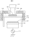
図1、図2にそれぞれ本実施例に係るECR方式のドライエッチング装置の全体構成図とそれに用いるスロットアンテナ板の平面図を示す。プラズマ電源101から放出された電磁波が導波管102、空洞共振部103、アンテナ板104と石英板106を介してチャンバ(真空容器)107中へ放出される。アンテナ板104には図2のように外周部にスロット105が入っている。
A first embodiment will be described with reference to FIGS.
FIG. 1 and FIG. 2 are an overall configuration diagram of an ECR type dry etching apparatus according to the present embodiment and a plan view of a slot antenna plate used therefor. An electromagnetic wave emitted from the
ドライエッチングのプロセスにおいては、チャンバ107内はエッチングガスが一定の圧力で保持されており、電磁波によりガスがプラズマ化して反応性イオンがウエハ110に入射することでエッチングが進行する。なお、ここではウエハの直径を300mmとしたが、それ以上の直径のウエハを用いることができる。ウエハ110を保持する試料台109には、入射イオンを加速するためのバイアス電源111が接続されている。この装置では電磁コイル108によりチャンバ107内に磁場を発生する。プラズマ中の電子サイクロトロン運動の周波数と、プラズマ電源101の周波数が一致するように磁場強度を設定すると、電子サイクロトロン共鳴が生じて電力が効率よくプラズマに吸収されて、低圧にて高いプラズマ密度を維持することができる。なお図では真空排気ポンプやガス導入系、装置全体を制御する制御部等は省略している。
In the dry etching process, the etching gas is held in the
試料台109に時間応答が速いプラズマ密度計測用のプローブを設置してプラズマ密度の時間変化を測定した。その結果、試料台109の外周部ではプラズマ密度が約50msで定常値になるが、ウエハ中心部は定常値に至るまで約150msかかることが判明した。定常状態ではウエハ中心部のプラズマ密度が外周部より高くなる。これはマイクロ波電力をチャンバの外周部から導入しているので、瞬間的には外周部でプラズマ密度が高くなるが約150ms後には、発生したプラズマが磁場を横切って拡散して定常状態になることを意味している。一方、マイクロ波電力をオフすると外周部でプラズマ密度は約4msで半減し、8ms後に0になった。ウエハ中心部では9msで密度が半減して、18ms後で0になった。なお、マイクロ波電力は90%以上が外周部からチャンバ内へ導入されることが望ましい。
A probe for plasma density measurement having a quick time response was installed on the
以上の結果から、マイクロ波を外周から導入すると同時に、定常状態になる前にプラズマをオフして、この点滅を周期的に繰り返せば、パルスのオン時間とオフ時間の調整により、プラズマ密度を制御できることが分かる。そこで、プラズマを発生する電力のオンオフを周期的に繰り返す制御手段(図示せず)を設けた。また、前記制御手段を、プラズマをオンしてからプラズマが定常状態に落ち着く前に前記電力をオフしてプラズマを消すものとした。なお、この制御手段は前記制御部(図示せず)に設けた。 From the above results, if the microwave is introduced from the outer periphery, the plasma density is controlled by adjusting the pulse ON time and OFF time if the plasma is turned off before the steady state is reached and this blinking is repeated periodically. I understand that I can do it. Therefore, a control means (not shown) is provided that periodically turns on and off the power for generating plasma. In addition, the control means turns off the plasma by turning off the power before the plasma settles in a steady state after turning on the plasma. This control means is provided in the control section (not shown).
プラズマを発生する電力をチャンバ外周部から供給する電力導入手段と、前記電力のオンオフを周期的に繰り返す制御手段とを設けることにより均一性が改善される。更に、この制御手段により、プラズマが発生して拡散して定常状態に落ち着く前に前記電力をオフしてプラズマを消すことにより、より均一性を向上することができる。 Uniformity is improved by providing power introduction means for supplying power for generating plasma from the outer periphery of the chamber and control means for periodically turning on and off the power. Further, this control means can improve the uniformity by turning off the power and turning off the plasma before the plasma is generated and diffused and settles to a steady state.
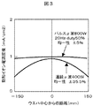
図3に図1に示す装置の試料台109上での飽和イオン電流(Icf)分布をプローブで測定した結果をしめす。試料台109の半径は180mmで、直径300mmのウエハに対応する。放電のガスはHBr 150ml/min /O2 5ml/min、圧力0.4Paとした。マイクロ波の電力を連続400Wとパルス放電でピーク電力800W、繰り返し周波数20Hz、デューティー比50%(平均マイクロ波電力400W)の比較をすると、均一性は連続放電時で±35.5%、パルス放電時で5%以内となった。つまり、マイクロ波電力をチャンバ107の外周部から導入するだけではプラズマ密度は均一化されず、マイクロ波電力のパルス化と合わせて初めて均一化される。このパルス条件ではマイクロ波電力のオン時間が50ms、オフ時間が50msになり、先に述べたようにプラズマが定常状態に達する前にプラズマをオフしており、予想した効果が表れていることがわかる。また、プラズマ密度の時間変化の計測より、プラズマのオン時間は150msより短くして、オフ時間はプラズマ密度がある程度まで低下する時間以上長くすればよいことが分かる。実験的にはオフ時間はプラズマ密度が50%以下に低下する時間以上にすれば、均一化の効果が表れることがわかった。プラズマを発生する電力オフ後、プラズマ密度が定常時の2分の1以下に落ち込んでからオンする制御は前記制御手段により行うことができる。以上のプラズマが定常状態に達するまでの時間は、ガスの圧力他の条件により異なるが、概念的には、マイクロ波電力を外周から導入して、かつ、プラズマが定常状態になる前にプラズマをオフして、これを繰り返せば、均一性を向上できる。またオンオフ時間の調整により、均一性を制御できる。また、あるガス種や圧力における最適なオンオフ時間は上記の値を目安としてエッチング速度の均一性などをモニタしながら実験的に決定できる。
FIG. 3 shows the result of measuring the saturation ion current (Icf) distribution on the
以上示したように、本実施例によれば、プラズマを発生する電力をチャンバ外周部から供給する電力導入手段と前記電力のオンオフ周期的に繰り返す制御手段を設けることにより、大口径ウエハをECR方式でドライエッチングするような場合であっても、エッチング速度など処理特性のウエハ面内均一性を向上することができる半導体製造装置を提供することができる。また、前記制御手段により、プラズマが発生して拡散して定常状態に落ち着く前に前記電力をオフしてプラズマを消すことで、より均一性を向上することができる。また、前記制御手段により、前記電力オフ後、プラズマ密度が定常時の2分の1以下に落ち込んでから前記電力をオンすることは均一性向上に有効である。更に、これらのオンオフを制御するに際し、事前に測定したデータを用いることにより、効果的に均一性を向上させることができる。 As described above, according to the present embodiment, the ECR system is used for the large-diameter wafer by providing the power introduction means for supplying the power for generating plasma from the outer periphery of the chamber and the control means for periodically repeating the power on / off. Even when dry etching is performed, a semiconductor manufacturing apparatus capable of improving in-wafer uniformity of processing characteristics such as etching rate can be provided. Further, the control means can turn off the power and extinguish the plasma before the plasma is generated and diffused and settles to a steady state, thereby improving the uniformity. In addition, it is effective for improving the uniformity that the control means turns on the power after the power is turned off after the plasma density falls to one-half or less of the steady state. Furthermore, when controlling these on / off operations, uniformity can be effectively improved by using data measured in advance.
また以上の実施例ではμ波電力のパルス化において、オフ時にはμ波を0Wにする場合を述べたが、必ずしも完全に0Wにする必要はない。本質的にはオフ時のμ波電力をオン時の電力より小さくしてプラズマ密度がピーク時の50%以下になるようにすればよい。本実施例の条件ではオン時のμ波800Wに対してオフ時のマイクロ波を200W以下にしてやれば、完全に0Wにするのと同じ均一性改善が得られた。オフ時の電力を何W以下に設定すればよいかはガスや圧力などの条件により異なるので、個々の条件において予め均一性のデータを取得し、そのデータに基づいて値を決定すればよい。 In the above embodiment, in the case of pulsing the μ-wave power, the case where the μ-wave is set to 0 W when turned off has been described, but it is not always necessary to set it to 0 W completely. Essentially, the microwave power at the time of off may be made smaller than the power at the time of on so that the plasma density is 50% or less of the peak. Under the conditions of this example, if the microwave at the time of OFF was set to 200 W or less with respect to the 800 μW of the μ wave at the time of ON, the same uniformity improvement as that of completely setting to 0 W was obtained. Since how much power should be set when turning off depends on conditions such as gas and pressure, uniformity data is acquired in advance under each condition, and a value may be determined based on the data.
第2の実施例について図4〜図7を用いて説明する。なお、実施例1に記載され、本実施例に未記載の事項は特段の事情がない限り本実施例にも適用することができる。なお、本実施例で用いた半導体製造装置はアンテナを除き実施例1に示したものと同様である。 A second embodiment will be described with reference to FIGS. Note that the items described in the first embodiment and not described in the present embodiment can be applied to the present embodiment unless there are special circumstances. The semiconductor manufacturing apparatus used in this example is the same as that shown in Example 1 except for the antenna.
本実施例では、アンテナに設けるスロットの設置範囲を変更した例について述べる。図4はアンテナの概略平面図で、アンテナ板401にスロット402が半径r以上の範囲に複数段に分かれて設置されている。図5は半径rとプラズマ密度均一性の関係を示す図である。ガスはCl2 150ml/min/O2 3ml/min、圧力0.6Paで、マイクロ波電力をパルス放電でピーク電力1000W、繰り返し周波数20Hz、デューティー比50%(平均マイクロ波電力500W)とした。
In this embodiment, an example in which the installation range of slots provided in an antenna is changed will be described. FIG. 4 is a schematic plan view of an antenna.
試料台109の半径は180mmで、直径300mmのウエハに対応する。均一性は半径rが70mm以上でドライエッチングに適用できる目安である10%以下になった。すなわち、ウエハ半径の約2分の1以上の外周部からマイクロ波を導入すると均一性が確保できる。ウエハ直径が450mmに対応する装置では、半径110mm以上の範囲からマイクロ波電力を導入すればよい。
The radius of the
図6はアンテナの別実施例でアンテナ板601に同心円状のスロット602が入っている。また図7では長方形状のスロット702が平行にアンテナ板701の外周同心円状に配置されている。いずれのアンテナにおいても、外周からマイクロ波を導入するスロット形状とその配置は他にも各種あるが、スロットをウエハ半径の2分の1以上の範囲に設置することで、同様な効果が得られる。
FIG. 6 shows another embodiment of the antenna. An
以上示したように、本実施例によれば、直径が300mm以上の大口径ウエハをECR方式でドライエッチングするような場合であっても、エッチング速度など処理特性のウエハ面内均一性を向上することができる半導体製造装置を提供することができる。また、アンテナに設けるスロットはウエハ半径の2分の1以上の範囲に設置することにより、実用的な均一性が得られる。 As described above, according to the present embodiment, even in the case where a large-diameter wafer having a diameter of 300 mm or more is dry-etched by the ECR method, the in-wafer uniformity of processing characteristics such as an etching rate is improved. The semiconductor manufacturing apparatus which can be provided can be provided. Moreover, practical uniformity can be obtained by installing the slot provided in the antenna within a range of one half or more of the wafer radius.
第3の実施例について図8〜図9を用いて説明する。なお、実施例1又は2に記載され、本実施例に未記載の事項は特段の事情がない限り本実施例にも適用することができる。 A third embodiment will be described with reference to FIGS. Note that the matters described in the first or second embodiment and not described in the present embodiment can be applied to the present embodiment unless there are special circumstances.
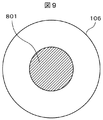
図8は本実施例に係るドライエッチングを行う半導体製造装置の概略全体構成図であり、マイクロ波電力を外周導入する別の例を示す。図9に本半導体製造装置で用いる石英板106部分の概略平面図を示す。ここでは、石英板106の中央部にフェライトやグラファイトなどのマイクロ波吸収体801を配置している。この構造では、中心部のマイクロ波が吸収されることにより、電界強度が弱くなり、放電点灯時には外周部のプラズマ密度が大きくなる。マイクロ波吸収体でのマイクロ波の吸収量が90%以上(透過量が10%以下)なら実用上使用することができる。本マイクロ波吸収体を用いることにより、実施例1と同様に放電をパルス化することで、プラズマ密度の均一性を改善できる。この場合、マイクロ波吸収体の設置範囲をウエハ半径の2分の1以上にすればよい。
FIG. 8 is a schematic overall configuration diagram of a semiconductor manufacturing apparatus that performs dry etching according to the present embodiment, and shows another example in which microwave power is introduced into the outer periphery. FIG. 9 shows a schematic plan view of the
以上示したように、本実施例によれば、大口径ウエハをECR方式でドライエッチングするような場合であっても、エッチング速度など処理特性のウエハ面内均一性を向上することができる半導体製造装置を提供することができる。 As described above, according to the present embodiment, even when a large-diameter wafer is dry-etched by the ECR method, it is possible to improve the in-wafer uniformity of processing characteristics such as an etching rate. An apparatus can be provided.
以上の実施例では、ECR方式のドライエッチング装置を例に説明したが、本発明はたとえばヘリコン波のプラズマ中の伝搬を利用したプラズマ源など、電界をプラズマ中に伝搬させる方式のプラズマ源に適用して、同様の効果を得ることができる。また、電磁波の周波数は2.45GHzに限らず、たとえばUHF帯の電磁波を用いても同様の効果がある。また、プラズマ源の利用範囲はドライエッチングに限らず、ケミカルベーパーデポジション(CVD)などに用いるプラズマ源でも同様に均一性を改善ができる。 In the above embodiments, the ECR dry etching apparatus has been described as an example. However, the present invention is applied to a plasma source that propagates an electric field in plasma, such as a plasma source that uses propagation of helicon waves in plasma. Thus, the same effect can be obtained. Further, the frequency of the electromagnetic wave is not limited to 2.45 GHz, and the same effect can be obtained by using, for example, an electromagnetic wave in the UHF band. Further, the application range of the plasma source is not limited to dry etching, and the uniformity can be improved in the same manner even in a plasma source used for chemical vapor deposition (CVD) or the like.
以上、本願発明を詳細に説明したが、以下に主な発明の形態を列挙する。
(1) 内部を真空にできるチャンバと、前記チャンバの中にプラズマを生成するための電源と、前記電源からの電力を前記チャンバ内へ導く導波路と、前記電源を含む装置全体を制御する制御部とを備えた半導体製造装置において、
前記電力を前記チャンバの外周部から前記チャンバ内へ導入する手段を更に有し、
前記制御部は、前記電力を周期的にオンオフする制御手段を含むことを特徴とする半導体製造装置。
(2) 内部を真空にできるチャンバと、前記チャンバの中にプラズマを生成するための電源と、前記電源からの電力を前記チャンバ内へ導く導波路と、前記電源を含む装置全体を制御する制御部と、前記チャンバ内に設けられた試料台とを備えた半導体製造装置において、
前記電力を前記チャンバの外周部から前記チャンバ内へ導入する電力導入手段を更に有し、
前記制御部は、前記電力を周期的にオンオフする制御手段を含み、
前記電力導入手段は、前記電力を、前記試料台に載置される半導体ウエハの半径の2分の1より外側の部分から導入するものであることを特徴とする半導体製造装置。
(3) 上記(1)又は(2)に記載の半導体製造装置において、
前記電力導入手段は、外周部にスロットが設けられたアンテナ板であることを特徴とする半導体製造装置。
(4) 上記(1)又は(2)に記載の半導体製造装置において、
前記電力導入手段は、前記チャンバ上部中央に設けられた電力吸収体であることを特徴とする半導体製造装置。
(5) 上記(1)乃至(4)のいずれか一に記載の半導体製造装置において、
前記プラズマは、磁場と電子サイクロトロン共鳴とを利用して生成されるものであることを特徴とする半導体製造装置。
(6) 上記(1)乃至(5)のいずれか一に記載の半導体製造装置において、
前記制御手段は、前記電力をオンした後、発生したプラズマが定常状態に至る前に前記電力をオフするものであることを特徴とする半導体製造装置。
(7) 上記(1)乃至(6)のいずれか一に記載の半導体製造装置において、
前記制御手段は、前記電力をオフした後、プラズマ密度が定常時の2分の1以下に落ち込んでから前記電力をオンするものであることを特徴とする半導体製造装置。
(8) 上記(1)乃至(5)のいずれか一項に記載の半導体製造装置において、
前記電力のオンからオフまでの時間は150msより短いことを特徴とする半導体製造装置。
(9) 上記(1)乃至(5)のいずれか一に記載の半導体製造装置において、
前記電力のオフからオンまでの時間は9msより長いことを特徴とする半導体製造装置。
(10) 上記(6)記載の半導体製造装置において、
前記制御手段は、事前に取得されたデータを用いて前記電力のオフの制御を行うものであることを特徴とする半導体製造装置。
(11) 上記(7)記載の半導体製造装置において、
前記制御手段は、事前に取得されたデータを用いて前記電力のオンの制御を行うものであることを特徴とする半導体製造装置。
Although the present invention has been described in detail above, the main invention modes are listed below.
(1) A chamber that can be evacuated, a power source for generating plasma in the chamber, a waveguide that guides power from the power source into the chamber, and a control that controls the entire apparatus including the power source. In a semiconductor manufacturing apparatus comprising a part,
Means for introducing the power from the outer periphery of the chamber into the chamber;
The semiconductor manufacturing apparatus according to claim 1, wherein the control unit includes control means for periodically turning on and off the power.
(2) A chamber capable of evacuating the interior, a power source for generating plasma in the chamber, a waveguide for guiding power from the power source into the chamber, and a control for controlling the entire apparatus including the power source In a semiconductor manufacturing apparatus comprising a portion and a sample stage provided in the chamber,
Further comprising power introduction means for introducing the power from the outer periphery of the chamber into the chamber;
The control unit includes control means for periodically turning on and off the power,
The semiconductor manufacturing apparatus according to claim 1, wherein the power introduction means introduces the power from a portion outside a half of a radius of the semiconductor wafer placed on the sample stage.
(3) In the semiconductor manufacturing apparatus according to (1) or (2) above,
The semiconductor manufacturing apparatus according to claim 1, wherein the power introduction means is an antenna plate having a slot provided in an outer peripheral portion.
(4) In the semiconductor manufacturing apparatus according to (1) or (2) above,
The semiconductor manufacturing apparatus according to claim 1, wherein the power introducing means is a power absorber provided at an upper center of the chamber.
(5) In the semiconductor manufacturing apparatus according to any one of (1) to (4),
2. The semiconductor manufacturing apparatus according to claim 1, wherein the plasma is generated using a magnetic field and electron cyclotron resonance.
(6) In the semiconductor manufacturing apparatus according to any one of (1) to (5),
The semiconductor manufacturing apparatus according to claim 1, wherein the control means turns off the power after the power is turned on and before the generated plasma reaches a steady state.
(7) In the semiconductor manufacturing apparatus according to any one of (1) to (6),
The semiconductor manufacturing apparatus according to claim 1, wherein after the power is turned off, the control means turns on the power after the plasma density drops to one-half or less of a steady state.
(8) In the semiconductor manufacturing apparatus according to any one of (1) to (5),
2. The semiconductor manufacturing apparatus according to claim 1, wherein a time from turning on to turning off the power is shorter than 150 ms.
(9) In the semiconductor manufacturing apparatus according to any one of (1) to (5),
2. The semiconductor manufacturing apparatus according to claim 1, wherein a time from turning off the power to turning on is longer than 9 ms.
(10) In the semiconductor manufacturing apparatus described in (6) above,
The semiconductor manufacturing apparatus characterized in that the control means controls the power off using data acquired in advance.
(11) In the semiconductor manufacturing apparatus described in (7) above,
The semiconductor manufacturing apparatus according to claim 1, wherein the control means controls the power on using data acquired in advance.
101:プラズマ電源、102:導波管、103:空洞共振部、104,401,601,701:アンテナ板、105,402,602,702:スロット、106:石英板、107:チャンバ、108:電磁コイル、109:試料台、110:ウエハ、111:バイアス電源、801:マイクロ波吸収体。 101: Plasma power source, 102: Waveguide, 103: Cavity resonance part, 104, 401, 601, 701: Antenna plate, 105, 402, 602, 702: Slot, 106: Quartz plate, 107: Chamber, 108: Electromagnetic Coil, 109: sample stage, 110: wafer, 111: bias power source, 801: microwave absorber.
Claims (11)
前記電力を前記チャンバの外周部から前記チャンバ内へ導入する電力導入手段を更に有し、
前記制御部は、前記電力を周期的にオンオフする第1の制御手段を含むことを特徴とする半導体製造装置。 A chamber capable of evacuating the interior; a power source for generating plasma in the chamber; a waveguide for guiding power from the power source into the chamber; and a controller for controlling the entire apparatus including the power source. In the semiconductor manufacturing apparatus provided,
Further comprising power introduction means for introducing the power from the outer periphery of the chamber into the chamber;
The semiconductor manufacturing apparatus according to claim 1, wherein the control unit includes first control means for periodically turning on and off the power.
前記電力を前記チャンバの外周部から前記チャンバ内へ導入する電力導入手段を更に有し、
前記制御部は、前記電力を周期的にオンオフする第1の制御手段を含み、
前記電力導入手段は、前記電力を、前記試料台に載置される半導体ウエハの半径の2分の1より外側の部分から導入するものであることを特徴とする半導体製造装置。 A chamber capable of evacuating the interior; a power source for generating plasma in the chamber; a waveguide for guiding power from the power source into the chamber; and a controller for controlling the entire apparatus including the power source; In a semiconductor manufacturing apparatus provided with a sample stage provided in the chamber,
Further comprising power introduction means for introducing the power from the outer periphery of the chamber into the chamber;
The control unit includes first control means for periodically turning on and off the power,
The semiconductor manufacturing apparatus according to claim 1, wherein the power introduction means introduces the power from a portion outside a half of a radius of the semiconductor wafer placed on the sample stage.
前記電力導入手段は、外周部にスロットが設けられたアンテナ板であることを特徴とする半導体製造装置。 In the semiconductor manufacturing apparatus according to claim 1 or 2,
The semiconductor manufacturing apparatus according to claim 1, wherein the power introduction means is an antenna plate having a slot provided in an outer peripheral portion.
前記電力導入手段は、前記チャンバ上部中央に設けられた電力吸収体であることを特徴とする半導体製造装置。 In the semiconductor manufacturing apparatus according to claim 1 or 2,
The semiconductor manufacturing apparatus according to claim 1, wherein the power introducing means is a power absorber provided at an upper center of the chamber.
前記プラズマは、磁場と電子サイクロトロン共鳴を利用して生成されるものであることを特徴とする半導体製造装置。 The semiconductor manufacturing apparatus according to any one of claims 1 to 4,
The semiconductor manufacturing apparatus, wherein the plasma is generated using a magnetic field and electron cyclotron resonance.
前記制御手段は、前記電力をオンした後、発生したプラズマが定常状態に至る前に前記電力をオフするものであることを特徴とする半導体製造装置。 The semiconductor manufacturing apparatus according to any one of claims 1 to 5,
The semiconductor manufacturing apparatus according to claim 1, wherein the control means turns off the power after the power is turned on and before the generated plasma reaches a steady state.
前記制御手段は、前記電力をオフした後、プラズマ密度が定常時の2分の1以下に落ち込んでから前記電力をオンするものであることを特徴とする半導体製造装置。 The semiconductor manufacturing apparatus according to any one of claims 1 to 6,
The semiconductor manufacturing apparatus according to claim 1, wherein after the power is turned off, the control means turns on the power after the plasma density drops to one-half or less of a steady state.
前記電力のオンからオフまでの時間は150msより短いことを特徴とする半導体製造装置。 The semiconductor manufacturing apparatus according to any one of claims 1 to 5,
2. The semiconductor manufacturing apparatus according to claim 1, wherein a time from turning on to turning off the power is shorter than 150 ms.
前記電力のオフからオンまでの時間は9msより長いことを特徴とする半導体製造装置。 The semiconductor manufacturing apparatus according to any one of claims 1 to 5,
2. The semiconductor manufacturing apparatus according to claim 1, wherein a time from turning off the power to turning on is longer than 9 ms.
前記制御手段は、事前に取得されたデータを用いて前記電力のオフの制御を行うものであることを特徴とする半導体製造装置。 The semiconductor manufacturing apparatus according to claim 6,
The semiconductor manufacturing apparatus characterized in that the control means controls the power off using data acquired in advance.
前記制御手段は、事前に取得されたデータを用いて前記電力のオンの制御を行うものであることを特徴とする半導体製造装置。 The semiconductor manufacturing apparatus according to claim 7,
The semiconductor manufacturing apparatus according to claim 1, wherein the control means controls the power on using data acquired in advance.
Priority Applications (1)
| Application Number | Priority Date | Filing Date | Title |
|---|---|---|---|
| JP2010184889A JP2012044035A (en) | 2010-08-20 | 2010-08-20 | Semiconductor manufacturing apparatus |
Applications Claiming Priority (1)
| Application Number | Priority Date | Filing Date | Title |
|---|---|---|---|
| JP2010184889A JP2012044035A (en) | 2010-08-20 | 2010-08-20 | Semiconductor manufacturing apparatus |
Publications (2)
| Publication Number | Publication Date |
|---|---|
| JP2012044035A true JP2012044035A (en) | 2012-03-01 |
| JP2012044035A5 JP2012044035A5 (en) | 2013-09-05 |
Family
ID=45899990
Family Applications (1)
| Application Number | Title | Priority Date | Filing Date |
|---|---|---|---|
| JP2010184889A Pending JP2012044035A (en) | 2010-08-20 | 2010-08-20 | Semiconductor manufacturing apparatus |
Country Status (1)
| Country | Link |
|---|---|
| JP (1) | JP2012044035A (en) |
Cited By (2)
| Publication number | Priority date | Publication date | Assignee | Title |
|---|---|---|---|---|
| JPWO2021220551A1 (en) * | 2020-04-27 | 2021-11-04 | ||
| CN116390320A (en) * | 2023-05-30 | 2023-07-04 | 安徽农业大学 | Electron cyclotron resonance discharge device and application |
Citations (6)
| Publication number | Priority date | Publication date | Assignee | Title |
|---|---|---|---|---|
| JPH065386A (en) * | 1992-06-19 | 1994-01-14 | Kobe Steel Ltd | Electronic cyclotron resonance device |
| JPH09289099A (en) * | 1996-02-20 | 1997-11-04 | Hitachi Ltd | Plasma processing method and device |
| JP2000331998A (en) * | 1999-05-21 | 2000-11-30 | Hitachi Ltd | Plasma processing device |
| JP2005019346A (en) * | 2003-06-30 | 2005-01-20 | Tokyo Electron Ltd | Plasma treatment device, plasma radiation antenna used for this and wave guide |
| JP2006190877A (en) * | 2005-01-07 | 2006-07-20 | Tokyo Electron Ltd | Plasma treatment method |
| JP2008130904A (en) * | 2006-11-22 | 2008-06-05 | Tokyo Electron Ltd | Manufacturing method of solar battery, and manufacturing device of solar battery |
-
2010
- 2010-08-20 JP JP2010184889A patent/JP2012044035A/en active Pending
Patent Citations (6)
| Publication number | Priority date | Publication date | Assignee | Title |
|---|---|---|---|---|
| JPH065386A (en) * | 1992-06-19 | 1994-01-14 | Kobe Steel Ltd | Electronic cyclotron resonance device |
| JPH09289099A (en) * | 1996-02-20 | 1997-11-04 | Hitachi Ltd | Plasma processing method and device |
| JP2000331998A (en) * | 1999-05-21 | 2000-11-30 | Hitachi Ltd | Plasma processing device |
| JP2005019346A (en) * | 2003-06-30 | 2005-01-20 | Tokyo Electron Ltd | Plasma treatment device, plasma radiation antenna used for this and wave guide |
| JP2006190877A (en) * | 2005-01-07 | 2006-07-20 | Tokyo Electron Ltd | Plasma treatment method |
| JP2008130904A (en) * | 2006-11-22 | 2008-06-05 | Tokyo Electron Ltd | Manufacturing method of solar battery, and manufacturing device of solar battery |
Cited By (6)
| Publication number | Priority date | Publication date | Assignee | Title |
|---|---|---|---|---|
| JPWO2021220551A1 (en) * | 2020-04-27 | 2021-11-04 | ||
| WO2021220551A1 (en) * | 2020-04-27 | 2021-11-04 | 株式会社日立ハイテク | Plasma treatment device |
| WO2021220329A1 (en) * | 2020-04-27 | 2021-11-04 | 株式会社日立ハイテク | Plasma treatment device |
| JP7139528B2 (en) | 2020-04-27 | 2022-09-20 | 株式会社日立ハイテク | Plasma processing equipment |
| TWI800798B (en) * | 2020-04-27 | 2023-05-01 | 日商日立全球先端科技股份有限公司 | Plasma treatment device |
| CN116390320A (en) * | 2023-05-30 | 2023-07-04 | 安徽农业大学 | Electron cyclotron resonance discharge device and application |
Similar Documents
| Publication | Publication Date | Title |
|---|---|---|
| KR101490628B1 (en) | Plasma processing apparatus and plasma processing method | |
| EP1984975B1 (en) | Method and apparatus for producing plasma | |
| KR101659594B1 (en) | High efficiency plasma source | |
| JP5668254B2 (en) | Control of plasma generation by specific gravity induced gas diffusion separation (GIGDS) method | |
| TWI536873B (en) | A low electron temperature microwave surface-wave plasma (swp) processing method and apparatus | |
| US20090045749A1 (en) | Plasma generating apparatus and plasma treatment apparatus | |
| US8828254B2 (en) | Plasma processing method | |
| US10418224B2 (en) | Plasma etching method | |
| JP2007273636A (en) | Apparatus and method for plasma treatment | |
| KR20170024922A (en) | Plasma generating apparatus | |
| KR101764767B1 (en) | Method and apparatus for plasma processing | |
| CN110391128B (en) | Remote modular high frequency source | |
| KR20180054495A (en) | Dual-frequency surface wave plasma source | |
| JP2012044035A (en) | Semiconductor manufacturing apparatus | |
| JP6991934B2 (en) | Plasma processing equipment | |
| US7779783B2 (en) | Plasma processing device | |
| KR20030067299A (en) | Device for prducing inductively coupled plasma and method | |
| JP2007035411A (en) | Plasma treatment device | |
| KR101022767B1 (en) | Plasma generation system | |
| JP2000164394A (en) | Plasma treating device | |
| KR20210055743A (en) | Plasma treatment method and plasma treatment apparatus | |
| JP5667368B2 (en) | Plasma processing equipment | |
| WO2022044216A1 (en) | Plasma treatment device | |
| JP2011187507A (en) | Apparatus and method of plasma processing | |
| JP2016100312A (en) | Plasma processing device and plasma processing method |
Legal Events
| Date | Code | Title | Description |
|---|---|---|---|
| A521 | Written amendment |
Free format text: JAPANESE INTERMEDIATE CODE: A523 Effective date: 20130719 |
|
| A621 | Written request for application examination |
Free format text: JAPANESE INTERMEDIATE CODE: A621 Effective date: 20130719 |
|
| A977 | Report on retrieval |
Free format text: JAPANESE INTERMEDIATE CODE: A971007 Effective date: 20140522 |
|
| A131 | Notification of reasons for refusal |
Free format text: JAPANESE INTERMEDIATE CODE: A131 Effective date: 20140610 |
|
| A02 | Decision of refusal |
Free format text: JAPANESE INTERMEDIATE CODE: A02 Effective date: 20141202 |