JP2016100312A - Plasma processing device and plasma processing method - Google Patents
Plasma processing device and plasma processing method Download PDFInfo
- Publication number
- JP2016100312A JP2016100312A JP2014239065A JP2014239065A JP2016100312A JP 2016100312 A JP2016100312 A JP 2016100312A JP 2014239065 A JP2014239065 A JP 2014239065A JP 2014239065 A JP2014239065 A JP 2014239065A JP 2016100312 A JP2016100312 A JP 2016100312A
- Authority
- JP
- Japan
- Prior art keywords
- microwave
- output
- plasma
- plasma processing
- processing
- Prior art date
- Legal status (The legal status is an assumption and is not a legal conclusion. Google has not performed a legal analysis and makes no representation as to the accuracy of the status listed.)
- Pending
Links
Images


Abstract
Description
本発明は、プラズマ処理装置及びプラズマ処理方法に関する。 The present invention relates to a plasma processing apparatus and a plasma processing method.
例えば半導体装置の製造においては、マイクロ波を発振するマイクロ波発振器を利用して処理容器内でプラズマを励起させるプラズマ処理装置が用いられることが知られている。マイクロ波発振器としては、安価で、且つ、高出力のマイクロ波を発振することが可能なマグネトロンが用いられることが多い。 For example, in the manufacture of semiconductor devices, it is known that a plasma processing apparatus that excites plasma in a processing container using a microwave oscillator that oscillates microwaves is known. As the microwave oscillator, a magnetron that is inexpensive and can oscillate a high-output microwave is often used.
このようなマイクロ波発振器においては、発振されるマイクロ波の特性は、種々の要因によって、目標とされる所望の特性から変動することがある。例えば、マイクロ波発振器は出力電力に対する周波数依存性を持つため、出力電力の大きさ(出力パワー)によって、発振されるマイクロ波の周波数(以下、単に「発振周波数」とも呼称する)が所望の周波数から変動することがある。また、マイクロ波発振器は、機械加工品であるため、複数のマイクロ波発振器同士の機械誤差によって、発振周波数が所望の周波数から変動したり、マイクロ波発振器の経年劣化によって所望の周波数が得られないといったこともある。 In such a microwave oscillator, the characteristics of the oscillated microwave may vary from a desired desired characteristic due to various factors. For example, since a microwave oscillator has frequency dependence on output power, the frequency of the microwave oscillated (hereinafter also simply referred to as “oscillation frequency”) depends on the magnitude of the output power (output power). May vary. In addition, since the microwave oscillator is a machined product, the oscillation frequency varies from the desired frequency due to mechanical errors between the plurality of microwave oscillators, or the desired frequency cannot be obtained due to aging of the microwave oscillator. There is also.
これに対して、所望の周波数から変動した発振周波数を調整する技術が種々検討されている。例えば、マイクロ波発振器の後段にインピーダンス発生器を設け、マイクロ波発振器に付与されるインピーダンスを変更することで、発振周波数を所望の周波数に調整する技術が知られている。また、所望の周波数と同一の周波数であり、マイクロ波発振器の出力電力よりも電力が低い基準信号をマイクロ波発振器に注入することで、発振周波数を基準信号の周波数に固定させる技術が知られている。 On the other hand, various techniques for adjusting the oscillation frequency fluctuating from a desired frequency have been studied. For example, a technique for adjusting an oscillation frequency to a desired frequency by providing an impedance generator at the subsequent stage of the microwave oscillator and changing the impedance applied to the microwave oscillator is known. Also known is a technique for fixing the oscillation frequency to the frequency of the reference signal by injecting into the microwave oscillator a reference signal having the same frequency as the desired frequency and lower than the output power of the microwave oscillator. Yes.
また、マイクロ波発振器(特にマグネトロン)の出力は単一の周波数ではなく、スペクトラムがある幅を持っており、スペクトラム特性(スペクトラムのピーク形状)が一定とはなりづらいといった事も知られている。 It is also known that the output of a microwave oscillator (especially magnetron) is not a single frequency but has a certain spectrum width, and the spectrum characteristics (spectrum peak shape) are not easily constant.
近年、処理時間の短縮化や効率化を図るため、半導体装置の製造等においてプラズマ処理装置を用いる際に、複数種のガスを用いた種々の処理工程をプラズマ放電を継続しつつ連続的に実施することが知られている(特許文献1、2参照)。この場合、各処理工程ごとに処理条件が異なるため、マイクロ波発振器の出力電力も処理条件ごとに異なり、出力電力を連続的に変更することが求められる場合がある。 In recent years, in order to shorten processing time and increase efficiency, when using plasma processing equipment in the manufacture of semiconductor devices, etc., various processing steps using multiple types of gases are continuously performed while plasma discharge continues. It is known (see Patent Documents 1 and 2). In this case, since the processing conditions are different for each processing step, the output power of the microwave oscillator is also different for each processing condition, and it may be required to continuously change the output power.
上述したように、マイクロ波発振器の発振周波数は出力電力の大きさによって変動する。また、マイクロ波発振器に対して出力電力を投入した際や、投入する出力電力を連続して変更した場合に、発振周波数が安定するまでに時間がかかることが知られていた。 As described above, the oscillation frequency of the microwave oscillator varies depending on the magnitude of the output power. Further, it has been known that it takes time for the oscillation frequency to stabilize when the output power is input to the microwave oscillator or when the output power to be input is continuously changed.
また、マイクロ波発振器の発振周波数におけるスペクトラム特性も、投入する出力電力が変わった場合には変動し、発振周波数が安定するには時間がかかってしまうといった問題もある。即ち、プロセス処理開始時や、プロセス条件を連続的に変更した場合等には、周波数と共にスペクトラム特性にもばらつきが生じ、プロセス処理に影響が出る恐れがある。 Further, the spectrum characteristic at the oscillation frequency of the microwave oscillator also changes when the input power to be input is changed, and there is a problem that it takes time for the oscillation frequency to be stabilized. That is, when the process processing is started or when the process conditions are continuously changed, the frequency characteristics and the spectrum characteristics also vary, which may affect the process processing.
特に、ラジアルラインスロットアンテナを介してマイクロ波によるプラズマ処理を行う処理装置では、アンテナに周波数特性があることが知られており、マイクロ波発振器の過渡的な周波数の変動が各プロセス処理に対してばらつき等の影響を及ぼす恐れがある。具体的には、マイクロ波を発振させた際や、出力電力を変えた際に、周波数が安定するまでに時間がかかることでプラズマの励起状態が変わり、インピーダンスの整合をとるためのチューナー等のポジションが変わりプラズマ生成のモードが変わってしまうといった問題が懸念される。 In particular, in a processing apparatus that performs plasma processing using microwaves via a radial line slot antenna, it is known that the antenna has frequency characteristics. There is a risk of variations. Specifically, when the microwave is oscillated or when the output power is changed, the excitation state of the plasma changes due to the time required for the frequency to stabilize, such as a tuner for impedance matching. There is a concern that the position changes and the plasma generation mode changes.
更には、マイクロ波発振器としてのマグネトロンにおいては、低い出力電力(例えば500W以下)で用いた場合、発振されるマイクロ波の周波数やそのスペクトラム特性が安定せず、実質的に低い出力電力では安定したマイクロ波発振器として用いることが困難であるといった問題があった。 Furthermore, in the case of a magnetron as a microwave oscillator, when used at a low output power (for example, 500 W or less), the frequency of the oscillated microwave and its spectrum characteristics are not stable, and stable at a substantially low output power. There was a problem that it was difficult to use as a microwave oscillator.
上記事情に鑑み、本発明の目的は、マイクロ波を発振するマイクロ波発振器を利用して処理容器内でプラズマを励起させるプラズマ処理装置において、プロセス処理開始時や、プロセス条件を連続的に変更した際に、所望のマイクロ波の発振周波数やスペクトラム特性をすばやく安定的に得ることが可能なプラズマ処理装置及びプラズマ処理方法を提供することにある。 In view of the above circumstances, an object of the present invention is to continuously change process conditions at the start of process processing or in a plasma processing apparatus that excites plasma in a processing container using a microwave oscillator that oscillates microwaves. At the same time, it is an object of the present invention to provide a plasma processing apparatus and a plasma processing method capable of quickly and stably obtaining a desired microwave oscillation frequency and spectrum characteristics.
また、出力パワーによらずマイクロ波の発振周波数やスペクトラム特性が一定となり、更には例えば500W以下といった低出力パワーにおいてもマイクロ波の発振周波数やスペクトラム特性が一定となるようなプラズマ処理装置及びプラズマ処理方法を提供することを目的とする。 Further, a plasma processing apparatus and plasma processing in which the microwave oscillation frequency and spectrum characteristics are constant regardless of the output power, and the microwave oscillation frequency and spectrum characteristics are constant even at a low output power of, for example, 500 W or less. It aims to provide a method.
前記の目的を達成するため、本発明によれば、被処理体を処理するプラズマ処理装置であって、被処理体を内部に収容してプラズマ処理を行う処理容器と、マイクロ波発振器を含み、前記マイクロ波発振器によって発振されるマイクロ波を用いて前記処理容器内にプラズマを発生させるプラズマ生成機構を備え、前記マイクロ波発振器は、当該マイクロ波発振器から発振されるマイクロ波の出力を、一方は前記処理容器内にプラズマを発生させる出力、他方は前記処理容器外に設けたダミー負荷に吸収させる出力として分配する出力分配機構と、前記出力分配機構におけるマイクロ波の出力分配比を制御する制御部と、を有することを特徴とする、プラズマ処理装置が提供される。 In order to achieve the above object, according to the present invention, there is provided a plasma processing apparatus for processing an object to be processed, which includes a processing vessel for accommodating the object to be processed and performing plasma processing, and a microwave oscillator, A plasma generation mechanism that generates plasma in the processing container using microwaves oscillated by the microwave oscillator, the microwave oscillator outputs an output of the microwave oscillated from the microwave oscillator, An output distribution mechanism that distributes an output for generating plasma in the processing container, and an output to be absorbed by a dummy load provided outside the processing container, and a control unit that controls an output distribution ratio of microwaves in the output distribution mechanism A plasma processing apparatus is provided.
上記プラズマ処理装置においては、前記出力分配機構と前記処理容器との間には方向性結合器を含む整合器が設けられ、前記方向性結合器には、前記出力分配機構において前記処理容器内にプラズマを発生させるために分配されたマイクロ波の進行波の電力信号を検出する検出器が設けられ、前記制御部は前記検出器で検出された電力信号に基づき前記出力分配機構におけるマイクロ波の出力分配比を制御しても良い。 In the plasma processing apparatus, a matching unit including a directional coupler is provided between the output distribution mechanism and the processing container, and the directional coupler is provided in the processing container by the output distribution mechanism. A detector for detecting a power signal of a traveling wave of a microwave distributed to generate plasma is provided, and the control unit outputs a microwave in the output distribution mechanism based on the power signal detected by the detector. The distribution ratio may be controlled.
上記プラズマ処理装置においては、前記マイクロ波発振器に電圧を供給する電源が設けられ、前記制御部は、前記出力分配機構におけるマイクロ波の出力分配比と、前記検出器で検出された電力信号に基づき前記マイクロ波発振器に供給される電圧を制御しても良い。 In the plasma processing apparatus, a power source for supplying a voltage to the microwave oscillator is provided, and the control unit is configured based on an output distribution ratio of the microwave in the output distribution mechanism and a power signal detected by the detector. The voltage supplied to the microwave oscillator may be controlled.
上記プラズマ処理装置においては、前記プラズマ生成機構は、前記マイクロ波発振器により発生させたマイクロ波を前記処理容器内へ透過させる誘電体窓と、複数のスロットが設けられ、前記マイクロ波を前記誘電体窓に放射するスロットアンテナ板と、を含んでも良い。 In the plasma processing apparatus, the plasma generation mechanism is provided with a dielectric window for transmitting the microwave generated by the microwave oscillator into the processing container and a plurality of slots, and the microwave is transmitted to the dielectric. And a slot antenna plate that radiates to the window.
上記プラズマ処理装置においては、前記マイクロ波発振器から発振されるマイクロ波の出力は500W超5000W以下であっても良い。また、前記マイクロ波発振器はマグネトロンを備えても良い。 In the plasma processing apparatus, the output of the microwave oscillated from the microwave oscillator may be more than 500 W and not more than 5000 W. The microwave oscillator may include a magnetron.
また、別な観点からの本発明によれば、内部でプラズマ処理を行う処理容器と、マイクロ波発振器を含み、前記マイクロ波発振器によって発振されるマイクロ波を用いて前記処理容器内にプラズマを発生させるプラズマ生成機構と、を備えたプラズマ処理装置を用い、被処理体に処理を行うプラズマ処理方法であって、前記マイクロ波発振器から発振されるマイクロ波の出力を、一方は前記処理容器内にプラズマを発生させる出力、他方は前記処理容器外に設けたダミー負荷に吸収させる出力として出力分配機構によって分配させ、当該分配された一方の出力のマイクロ波を用いて前記処理容器内にプラズマを発生させてプラズマ処理を行うことを特徴とする、プラズマ処理方法が提供される。 Further, according to the present invention from another viewpoint, a plasma is generated in the processing container using a microwave oscillated by the microwave oscillator, including a processing container for performing plasma processing inside and a microwave oscillator. A plasma processing method for processing a target object using a plasma processing apparatus comprising: a plasma generating mechanism for generating a microwave output oscillated from the microwave oscillator, one in the processing container An output distributing mechanism distributes the output for generating plasma and the other to be absorbed by a dummy load provided outside the processing container, and generates plasma in the processing container by using the microwave of the one output. A plasma processing method is provided, in which plasma processing is performed.
上記プラズマ処理方法においては、前記被処理体の処理は、連続する複数のプラズマ処理工程からなり、前記複数のプラズマ処理工程は、それぞれ異なる所定の出力のマイクロ波を用いて前記処理容器内にプラズマを発生させて行われ、前記マイクロ波発振器から発振されるマイクロ波の出力を一定とし、前記出力分配機構におけるマイクロ波の出力分配比を制御することで、前記連続する複数のプラズマ処理工程においてプラズマを発生させるためのマイクロ波の出力を各工程ごとの所定の値に連続的に変化させても良い。 In the plasma processing method, the processing of the object to be processed includes a plurality of continuous plasma processing steps, and the plurality of plasma processing steps use plasmas having different predetermined outputs, respectively, to generate plasma in the processing container. In the plurality of continuous plasma processing steps by controlling the microwave output distribution ratio in the output distribution mechanism by making the output of the microwave oscillated from the microwave oscillator constant. The output of the microwave for generating the signal may be continuously changed to a predetermined value for each step.
上記プラズマ処理方法においては、前記マイクロ波発振器から発振されるマイクロ波の出力は500W超5000W以下であっても良い。また、前記マイクロ波発振器はマグネトロンを備えても良い。 In the plasma processing method, the output of the microwave oscillated from the microwave oscillator may be more than 500 W and not more than 5000 W. The microwave oscillator may include a magnetron.
本発明によれば、マイクロ波を発振するマイクロ波発振器を利用して処理容器内でプラズマを励起させるプラズマ処理装置において、プロセス処理開始時や、プロセス条件を連続的に変更した際に、所望のマイクロ波の発振周波数やスペクトラム特性をすばやく安定的に得ることが可能となる。
また、出力パワーによらずマイクロ波の発振周波数やスペクトラム特性が一定となり、更には例えば500W以下といった低出力パワーにおいてもマイクロ波の発振周波数やスペクトラム特性が一定となるようなプラズマ処理装置及びプラズマ処理方法が実現できる。
According to the present invention, in a plasma processing apparatus that excites plasma in a processing container using a microwave oscillator that oscillates microwaves, when a process process is started or when process conditions are continuously changed, a desired value is obtained. It becomes possible to obtain the oscillation frequency and spectrum characteristics of the microwave quickly and stably.
Further, a plasma processing apparatus and plasma processing in which the microwave oscillation frequency and spectrum characteristics are constant regardless of the output power, and the microwave oscillation frequency and spectrum characteristics are constant even at a low output power of, for example, 500 W or less. A method can be realized.
以下、本発明の実施の形態について図面を参照して説明する。なお、本明細書および図面において、実質的に同一の機能構成を有する構成要素については、同一の符号を付することにより重複説明を省略する。なお、本実施の形態のプラズマ処理装置1では、被処理体としてのウェハWの表面に対してプラズマCVD(Chemical Vapor Deposiotion)処理を行い、当該ウェハWの表面にSiN膜(シリコン窒化膜)を形成する場合を例として挙げて説明する。 Hereinafter, embodiments of the present invention will be described with reference to the drawings. In the present specification and drawings, components having substantially the same functional configuration are denoted by the same reference numerals, and redundant description is omitted. In the plasma processing apparatus 1 according to the present embodiment, a plasma CVD (Chemical Vapor Deposition) process is performed on the surface of the wafer W as an object to be processed, and a SiN film (silicon nitride film) is formed on the surface of the wafer W. The case of forming will be described as an example.
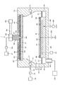
プラズマ処理装置1は、図1に示すように処理容器10を有している。処理容器10は、天井面が開口した略円筒形状を有し、当該天井面開口部には後述するラジアルラインスロットアンテナ40が配置されている。また、処理容器10の側面には、開口部としてのウェハWの搬入出口11が形成され、当該搬入出口11にはゲートバルブ12が設けられている。そして、処理容器10はその内部を密閉可能に構成されている。これら搬入出口11やゲートバルブ12の構成については、図1では簡略的に図示し、詳細な構成等については、図2等を参照して後述する。なお、処理容器10にはアルミニウム又はステンレス鋼等の金属が用いられ、処理容器10は接地されている。
The plasma processing apparatus 1 has a
処理容器10の底面には、ウェハWを載置する載置部としての載置台20が設けられている。載置台20は円筒形状を有し、また載置台20には例えばアルミニウムが用いられる。
On the bottom surface of the
載置台20の上面には静電チャック21が設けられている。静電チャック21は、絶縁材の間に電極22が挟み込まれた構成を有している。電極22は処理容器10の外部に設けられた直流電源23に接続されている。この直流電源23により載置台20の表面にクーロン力を生じさせて、ウェハWを載置台20上に静電吸着することができる。
An
また載置台20には、コンデンサ24を介して、RFバイアス用の高周波電源25が接続されていてもよい。高周波電源25は、ウェハWに引き込むイオンのエネルギーを制御するのに適した一定の周波数、例えば13.56MHzの高周波を所定のパワーで出力する。
Further, a high
また載置台20の内部には、例えば冷却媒体を流通させる温度調節機構26が設けられている。温度調節機構26は、冷却媒体の温度を調整する液温調節部27に接続されている。そして、液温調節部27によって冷媒媒体の温度が調節され、載置台20の温度を制御でき、この結果、載置台20上に載置されたウェハWを所定の温度に維持できる。なお、載置台20には、ウェハWの裏面に伝熱媒体、例えばHeガスなどを所定圧力(バックプレッシャー)にて供給するためのガス通路(図示せず)が形成されている。
In addition, a
載置台20の上面には、静電チャック21上のウェハWを囲むように環状のフォーカスリング28が設けられている。フォーカスリング28には例えばセラミックスあるいは石英などの絶縁性材料が用いられ、フォーカスリング28はプラズマ処理の均一性を向上させるように作用する。
An
なお、載置台20の下方には、ウェハWを下方から支持し昇降させるための昇降ピン(図示せず)が設けられている。昇降ピンは、載置台20に形成された貫通孔(図示せず)を挿通し載置台20の上面から突出可能になっている。 Below the mounting table 20, lifting pins (not shown) are provided for supporting the wafer W from below and lifting it. The elevating pins can be protruded from the upper surface of the mounting table 20 through a through hole (not shown) formed in the mounting table 20.
載置台20の周囲において、当該載置台20と処理容器10の側面との間には、環状の排気空間30が形成されている。排気空間30の上部には、処理容器10内を均一に排気するため、複数の排気孔が形成された環状のバッフル板31が設けられている。排気空間30の底部であって、処理容器10の底面には、排気管32が接続されている。排気管32の数は任意に設定でき、円周方向に複数形成されていてもよい。排気管32は、例えば真空ポンプを備えた排気装置33に接続されている。排気装置33は、処理容器10内の雰囲気を所定の真空度まで減圧することができる。
Around the mounting table 20, an
処理容器10の天井面開口部には、プラズマ生成用のマイクロ波を供給するラジアルラインスロットアンテナ40が設けられている。ラジアルラインスロットアンテナ40は、誘電体窓(マイクロ波透過板)41、スロット板42、遅波板43、シールド蓋体44を有している。
A radial
誘電体窓41は、例えばOリング等のシール材(図示せず)を介して、処理容器10の天井面開口部に密に設けられている。したがって、処理容器10の内部は気密に保持される。誘電体窓41には誘電体、例えば石英、Al2O3、AlN等が用いられ、誘電体窓41はマイクロ波を透過させる。
The
スロット板42は、誘電体窓41の上面であって、載置台20と対向するように設けられている。スロット板42には複数のスロットが形成され、スロット板42はアンテナとして機能する。スロット板42には、導電性を有する材料、たとえば銅、アルミニウム、ニッケル等が用いられる。
The
遅波板43は、スロット板42の上面に設けられている。遅波板43には低損失誘電体材料、例えば石英、Al2O3、AlN等が用いられ、遅波板43はマイクロ波の波長を短縮する。
The
シールド蓋体44は、遅波板43の上面において、遅波板43とスロット板42覆うように設けられている。シールド蓋体44の内部には、例えば冷却媒体を流通させる円環状の流路45が複数設けられている。流路45を流れる冷却媒体によって、誘電体窓41、スロット板42、遅波板43、シールド蓋体44が所定の温度に調節される。
The
シールド蓋体44の中央部には同軸導波管50が接続されている。同軸導波管50は、内部導体51と外管52を有している。内部導体51は、スロット板42と接続されている。内部導体51のスロット板42側は円錐形に形成されて、スロット板42に対してマイクロ波を効率よく伝播するようになっている。
A
同軸導波管50には、マイクロ波を所定の振動モードに変換するモード変換器53、矩形導波管54、マイクロ波を発振するマイクロ波発振器55が同軸導波管50側からこの順で接続されている。マイクロ波発振器55は、所定周波数、例えば2.45GHzのマイクロ波を発振させる。
The
かかる構成により、マイクロ波発振器55により発振されたマイクロ波は、矩形導波管54、モード変換器53、同軸導波管50を順次伝播し、ラジアルラインスロットアンテナ40内に供給され、遅波板43で圧縮され短波長化され、スロット板42で円偏波を発生させた後、スロット板42から誘電体窓41を透過して処理容器10内に放射される。このマイクロ波により処理容器10内では処理ガスがプラズマ化し、このプラズマによりウェハWのプラズマ処理が行われる。
With this configuration, the microwave oscillated by the
なお、上記ラジアルラインスロットアンテナ40(即ち、誘電体窓41、スロット板42、遅波板43、シールド蓋体44)とマイクロ波発振器55は、総じてプラズマ生成機構とされる。
The radial line slot antenna 40 (that is, the
処理容器10の天井面、すなわちラジアルラインスロットアンテナ40の中央部には、第1の処理ガス供給部としての第1の処理ガス供給管60が設けられている。第1の処理ガス供給管60はラジアルラインスロットアンテナ40を貫通し、当該第1の処理ガス供給管60の一端部はマイクロ波透過板41の下面において開口している。また、第1の処理ガス供給管60は同軸導波管50の内部導体51の内部を貫通し、さらにモード変換器53内を挿通して、当該第1の処理ガス供給管60の他端部は第1の処理ガス供給源61に接続されている。第1の処理ガス供給源61の内部には、処理ガスとして、例えばTSA(トリシリルアミン)、N2ガス、H2ガス、Arガスがそれぞれ個別に貯留されている。このうち、TSA、N2ガス、H2ガスはSiN膜の成膜用の原料ガスであり、Arガスはプラズマ励起用ガスである。なお、以下において、この処理ガスを「第1の処理ガス」という場合がある。また、第1の処理ガス供給管60には、第1の処理ガスの流れを制御するバルブや流量調節部等を含む供給機器群62が設けられている。
A first processing
図1に示すように処理容器10の側面には、第2の処理ガス供給部としての第2の処理ガス供給管70が設けられている。第2の処理ガス供給管70は、処理容器10の側面の円周上で等間隔に複数、例えば24本設けられている。第2の処理ガス供給管70の一端部は処理容器10の側面において開口し、他端部はバッファ部71に接続されている。第2の処理ガス供給管70は、その一端部が他端部より下方に位置するように斜めに配置されている。
As shown in FIG. 1, a second processing
バッファ部71は、処理容器10の側面内部に環状に設けられ、複数の第2の処理ガス供給管70に共通に設けられている。バッファ部71には、供給管72を介して第2の処理ガス供給源73が接続されている。第2の処理ガス供給源63の内部には、処理ガスとして、例えばTSA(トリシリルアミン)、N2ガス、H2ガス、Arガスがそれぞれ個別に貯留されている。なお、以下において、この処理ガスを「第2の処理ガス」という場合がある。また、供給管72には、第2の処理ガスの流れを制御するバルブや流量調節部等を含む供給機器群74が設けられている。
The
第1の処理ガス供給管60からの第1の処理ガスはウェハWの中心部に向けて供給され、第2の処理ガス供給管70からの第2の処理ガスはウェハWの外周部に向けて供給される。
The first processing gas from the first processing
なお、第1の処理ガス供給管60と第2の処理ガス供給管70から処理容器10内にそれぞれ供給される第1の処理ガス及び第2の処理ガスは、同種のガスでよいが、別種類のガスであってもよく、各々独立した流量で、或いは任意の流量比で供給することができる。
The first processing gas and the second processing gas respectively supplied from the first processing
次に、以上のように構成されたプラズマ処理装置1で行われるウェハWのプラズマ処理について説明する。本実施の形態では、上述したようにウェハWにプラズマ成膜処理を行って、当該ウェハWの表面にSiN膜を形成する。 Next, plasma processing of the wafer W performed by the plasma processing apparatus 1 configured as described above will be described. In the present embodiment, as described above, the plasma film forming process is performed on the wafer W to form the SiN film on the surface of the wafer W.
先ず、ゲートバルブ12を開き、処理容器10内にウェハWを搬入する。ウェハWは、昇降ピンによって載置台20上に載置される。このとき、直流電源23をオンにして静電チャック21の電極22に直流電圧を印加し、静電チャック21のクーロン力によりウェハWを静電チャック21上に静電吸着する。そして、ゲートバルブ12を閉じ、処理容器10内を密閉した後、排気装置33を作動させ、処理容器10内を所定の圧力、例えば400mTorr(=53Pa)に減圧する。
First, the
その後、第1の処理ガス供給管60から処理容器10内に第1の処理ガスを供給し、第2の処理ガス供給管70から処理容器10内に第2の処理ガスを供給する。このとき、第1の処理ガス供給管60から供給されるArガスの流量は例えば100sccm(mL/min)であり、第2の処理ガス供給管70から供給されるArガスの流量は例えば750sccm(mL/min)である。
Thereafter, the first processing gas is supplied from the first processing
このように処理容器10内に第1の処理ガス、第2の処理ガスが供給される際、マイクロ波発振器55を作動させ、当該マイクロ波発振器55において、例えば2.45GHzの周波数で所定のパワーのマイクロ波を発生させる。マイクロ波は、矩形導波管54、モード変換器53、同軸導波管50、ラジアルラインスロットアンテナ40を介して、処理容器10内に放射される。このマイクロ波によって処理容器10内では第1の処理ガス及び第2の処理ガスがプラズマ化し、プラズマ中で各処理ガスの解離が進み、その際に発生した活性種によってウェハW上に成膜処理がなされる。こうして、ウェハWの表面にSiN膜が形成される。
Thus, when the first processing gas and the second processing gas are supplied into the
ウェハWにプラズマ成膜処理を行っている間、高周波電源25をオンにして、例えば13.56MHzの周波数で所定のパワーの高周波を出力させてもよい。この高周波はコンデンサ24を介して載置台20に印加され、RFバイアスがウェハWに印加される。プラズマ処理装置1では、プラズマの電子温度を低く維持できるので、膜へのダメージがなく、しかも、高密度プラズマにより、処理ガスの分子が解離されやすいので、反応が促進される。また、適切な範囲でのRFバイアスの印加は、プラズマ中のイオンをウェハWへ引き込むように作用するため、SiN膜の緻密性を向上させるとともに、膜中のトラップを増加させるように作用する。
While performing the plasma film forming process on the wafer W, the high
その後、SiN膜が成長し、ウェハWに所定の膜厚のSiN膜が形成されると、第1の処理ガス、第2の処理ガスの供給と、マイクロ波の照射が停止される。その後、ウェハWは処理容器10から搬出されて、一連のプラズマ成膜処理が終了する。
Thereafter, when the SiN film is grown and the SiN film having a predetermined thickness is formed on the wafer W, the supply of the first processing gas and the second processing gas and the microwave irradiation are stopped. Thereafter, the wafer W is unloaded from the
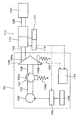
次に、上述した構成のプラズマ処理装置1に備えられるプラズマ生成機構に含まれるマイクロ波発振器55の具体的な構成について説明する。図2は、本実施の形態に係るマイクロ波発振器55の概略的な構成を示すブロック図である。
Next, a specific configuration of the
図2に示すように、マイクロ波発振器55は、マグネトロン100と、電源(いわゆるマグネトロン電源)102と、アイソレータ104と、出力分配機構106とを有する。また、マイクロ波発振器55は、出力分配機構106におけるマイクロ波の出力分配比を制御可能な制御部110を有する。また、マイクロ波発振器55外において、処理容器10等(同軸導波管50、モード変換器53、矩形導波管54を含む)である外部負荷120が、出力分配機構106の一方の出力端106aと導波管125を介して連通している。導波管125には、方向性結合器113を有する整合器114が設置されており、方向性結合器113には、検出器116、117が繋がっている。なお、検出器116は進行波電力を検出し、検出器117は反射波(後進波)電力を検出するものである。
As shown in FIG. 2, the
アイソレータ104はサーキュレータ104aとダミー負荷104bから構成され、マグネトロン100から入力されたマイクロ波を導波管108を介して出力分配機構106へ伝送すると共に、出力分配機構106側から反射されたマイクロ波(反射波)をダミー負荷104bに吸収させる。また、出力分配機構106はアイソレータ104を介してマグネトロン100から発振されたマイクロ波を分配・伝送する構成を有しており、一方の出力端106aは導波管125、整合器114を介してマイクロ波発振器55外の外部負荷120に連通し、他方の出力端106bはダミー負荷122に連通している。
The
上記ダミー負荷104bならびにダミー負荷122は、導波管内にマイクロ波を吸収しやすい材料を組み込み、マイクロ波によって暖められた材料を排熱する構成となっている。具体的には、マイクロ波を吸収しやすい材料は電波吸収体と呼ばれ、排熱には冷却水の循環や空冷ファン又は自然冷却を用いる。このときダミー負荷104b、122において反射波によって発生する電圧定在波比は1.2以下である。
The
マグネトロン100は、電源102から供給される電圧に応じて、高周波としてのマイクロ波を発振する。マグネトロン100は、マイクロ波を発生させるマイクロ波発生装置の一例を示すものである。ここで、マグネトロン100によって発振されるマイクロ波の周波数(以下、発振周波数とも呼称する)は、種々の要因によって、プロセス処理条件等に応じて目標とされる所望の周波数(以下、目標周波数とも呼称する)から変動することがある。具体的には、例えばマグネトロン100は、機械加工品であるため、複数のマグネトロン100同士の機械誤差によって発振周波数が目標周波数から変動する場合がある。また、マグネトロン100は、出力電力(出力パワーあるいは単に出力とも呼称される)に対する周波数依存性を持つため、出力電力の大きさによって、発振周波数が目標周波数から変動することがある。更には、マグネトロン100の経年劣化によって、発振周波数が目標周波数から変動することもある。
The
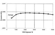
図3は、出力電力による発振周波数の変動を説明する説明図である。図3において横軸は、マグネトロン100から出力されたマイクロ波を方向性結合器113から検出器116で検出した出力電力(W)を示し、縦軸は、マグネトロン100の発振周波数(MHz)を示している。図3に示すように、マグネトロン100の発振周波数は、マグネトロン100の出力電力によって約±3MHz程度の範囲内において変動する。即ち、マグネトロン100の出力電力に応じてその発振周波数は変動し、目標周波数から変動してしまう場合があることが示されている。
FIG. 3 is an explanatory diagram for explaining the fluctuation of the oscillation frequency due to the output power. In FIG. 3, the horizontal axis indicates the output power (W) of the microwave output from the
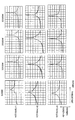
また、図4は、マグネトロン100から発振されるマイクロ波のスペクトラムの個体差ならびに出力電力に対する依存性についての説明図である。図4は、3種類のマグネトロン100(図中、マグネトロン1〜3)の出力電力をそれぞれ500W、1000W、3000W、5000Wにした際に発振されるマイクロ波のスペクトラムを示したものであり、縦軸はスペクトラム強度、横軸は発振周波数を示している。図4に示すように、マグネトロン100から発振されるマイクロ波のスペクトラムのピークは、3つのマグネトロン100(マグネトロン1〜3)ごとに異なり、また、出力電力によっても異なっている。即ち、マグネトロン100から発振されるマイクロ波のスペクトラムは、個体差があるのみならず、出力電力を変えるたびに変動し、そのピークが目標周波数から変動してしまう場合があることが示されている。なお、図4からは、マイクロ波のスペクトラムの波形は出力電力が大きくなる程、安定してピーク形状が観測されることが分かり、マグネトロン100の出力電力を大きくしてマイクロ波を発振させることでスペクトラム波形の安定したマイクロ波が得られることが分かる。
FIG. 4 is an explanatory diagram of individual differences in the spectrum of microwaves oscillated from the
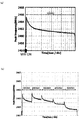
また、図5は、マグネトロン100から発振されるマイクロ波の周波数の経時的変動についての説明図であり、図5(a)は単一の出力電力(3000W)に対する周波数の経時的変動を示し、図5(b)は出力電力を連続的に複数の値に変えた際(1000W〜5000W)の周波数の経時的変動を示すものである。
図5(a)に示すように、マグネトロン100においてマイクロ波発振開始時(MWON時)に周波数は一時的に高くなり、その後経時的に周波数は減少していくことが分かる。
また、図5(b)に示すように、マグネトロン100において出力電力を上げた場合、一時的にマイクロ波の周波数が高くなり、その後同じ出力電力では経時的にマイクロ波の周波数は減少し、更に出力電力を高くした場合にも同様の挙動となる。なお、図5には図示していないが、出力電力を下げた場合には、一時的にマイクロ波の周波数は低くなり、その後同じ出力電力では経時的にマイクロ波の周波数は上昇するといった挙動となる。
即ち、マグネトロン100において、同じ出力電力でもってマイクロ波を発振したとしても、その周波数は経時的に変動し、更には、出力電力を連続的に複数の値に変えた際にも同様の挙動となることが分かる。
FIG. 5 is an explanatory diagram of the temporal variation of the frequency of the microwave oscillated from the
As shown in FIG. 5A, it can be seen that the frequency temporarily increases at the start of microwave oscillation (MWON) in the
Further, as shown in FIG. 5B, when the output power is increased in the
That is, in the
図2の説明に戻る。図2に示す電源102は、マイクロ波の発振に用いられる電圧をマグネトロン100に供給する電源であり、例えばアノード電源とフィラメント電源によって構成される。
Returning to the description of FIG. A
また、出力分配機構106は、いわゆるパワースプリッタとも呼ばれる装置であり、マグネトロン100から導波管108を介して伝送されたマイクロ波の出力を一方の出力端106aと他方の出力端106bとに分配する装置である。出力端106aから出力されたマイクロ波は、導波管125、整合器114を介して外部負荷120に伝送され、処理容器10内における処理ガスのプラズマ化に用いられる。一方、出力端106bから出力されたマイクロ波は、ダミー負荷122に吸収される構成となっている。一例として、マグネトロン100において出力電力5000Wで発振されたマイクロ波は、出力分配機構106に伝送された後、出力端106aからは出力電力3000Wのマイクロ波として外部負荷120に伝送され、出力端106bからは出力電力2000Wのマイクロ波がダミー負荷122に送られ吸収される。
The
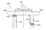
図6は、出力分配機構106の構成の一例を示す概略説明図である。図6に示すように、出力分配機構106には、一箇所の入力端130と、2つの出力端106a、106bが設けられている。また、出力分配機構106において、入力されたマイクロ波の分配比(出力分配比)を調整するための第1の調整部133が出力端106a側、第2の調整部134が出力端106b側に設けられている。これら入力端130、出力端106a、106bは連通する導波管によって構成されている。第1の調整部133には、伝搬するマイクロ波を反射する可動部材133aが設置され、第2の調整部134には、伝搬するマイクロ波を反射する可動部材134aが設置されている。
FIG. 6 is a schematic explanatory diagram illustrating an example of the configuration of the
図6に示すように、入力端130から入力されたマイクロ波の管内波長をλgとした場合に、第1の調整部133入口と第2の調整部134入口との間の距離はλg/2に設計され、これら第1の調整部133と第2の調整部134の中間に入力端130から入力されたマイクロ波が伝搬される構成となっている。ここで一例として、図示のように、例えば第1の調整部133の内部にはマイクロ波が伝搬しないように可動部材133aを配置し、第2の調整部134の内部にはマイクロ波が伝搬する距離をλg/4だけ確保するように可動部材134aを配置した場合を説明する。λg/4の奇数倍の距離が確保された出力側はオープン(開放)状態となり、λg/4の偶数倍の距離が確保された出力側はショート(短絡)状態となり、ショート側のみにマイクロ波が伝搬することが知られている。即ち、図示のような場合には、出力端106aにのみマイクロ波が伝搬し、出力端106bにはマイクロ波は伝搬しない。
As shown in FIG. 6, when the in-tube wavelength of the microwave input from the
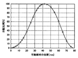
出力分配機構106は、上述した構成において可動部材133a、134aを好適な配置にすることで、出力端106aと出力端106bとに伝搬されるマイクロ波の比率を任意に調整することを可能にするものである。図7はこのように構成される出力分配機構106における可動部材133a、134aの位置と、出力端106a及び出力端106bに伝搬されるマイクロ波の分配比率との関係を示すグラフである。なお、図7には、一例として一方の可動部材(例えば可動部材133a)を基準点(0mm)から80mmまで動かした場合を示している。
The
図7に示すように、出力分配機構106においては、可動部材133a、134aを動かすことで、出力端106aと出力端106bに伝搬されるマイクロ波の比率(即ち、出力分配比)を任意の値に調整することができる。
As shown in FIG. 7, in the
図2の説明に戻る。マイクロ波発振器55には、出力分配機構106におけるマイクロ波の出力分配比を制御する制御部110が設けられている。図2の一点鎖線に示すように、検出器116で検出されたマイクロ波の進行波の電力信号に基づき、制御部110は最適な出力分配比を決定し、制御を行う。即ち、例えば外部負荷120においてプロセス処理が行われる場合に、プロセス条件に応じて設定される所定の出力電力のマイクロ波が検出器116にて検出されるような出力分配比でもって、マイクロ波の出力分配比が決定される。
一般的に知られるプラズマ処理装置でのプロセス処理は、出力電力500W超5000W以下のマイクロ波を用いるように設定されることから、マイクロ波発振器55から外部負荷120に対し、出力電力500W超5000W以下のマイクロ波が伝搬されるような出力分配比に制御される。
Returning to the description of FIG. The
Process processing in a generally known plasma processing apparatus is set to use microwaves having an output power of 500 W to 5000 W or less, and therefore, the output power of 500 W to 5000 W or less is applied to the
以下では、図2に示すように構成されるマイクロ波発振器55を用い、マイクロ波の出力電力の制御の具体的な流れについて説明する。
Below, the specific flow of control of the output power of a microwave is demonstrated using the
先ず、マグネトロン100の出力電力を一定に出力する。但し、この時の出力電力は、外部負荷120において使用するマイクロ波の出力電力以上とし、好ましくは、スペクトラムの波形が安定する例えば3000W以上の出力電力とする。
First, the output power of the
次に、マグネトロン100の出力開始時には、出力分配機構106により出力端106bに全てのマイクロ波が出力されるような分配比(即ち、出力端106a:出力端106b=0:100)とし、ダミー負荷122に全てのマイクロ波の出力を吸収させる。
Next, when the output of the
そして、ダミー負荷122に全てのマイクロ波の出力を吸収させた状態を、当該マイクロ波のスペクトラム波形が安定するまで続ける。例えば、マイクロ波のスペクトラム形状は、約30秒程度で安定する。このマイクロ波のスペクトラム波形の安定に要する時間を利用してプラズマ処理装置の起動、処理容器内のコンディションの調整、被処理体(ウェハW)の搬送等を行っても良い。これにより、スループットを低下させずにウェハWの処理を行うことができる。
Then, the state in which all the microwave outputs are absorbed by the
続いて、外部負荷120において必要とされるマイクロ波の出力電力が設定され、検出器116からの電力信号に基づき出力分配機構106の分配比が制御され、所定の分配比とされる。例えば外部負荷120において所定のプラズマ処理プロセスが行われる場合には、このように制御された分配比が所定のプロセス時間だけ保たれる。
Subsequently, the microwave output power required in the
ここで、外部負荷120におけるプラズマ処理プロセスのレシピを異なるものとする場合、前工程とは異なる出力電力のマイクロ波が要求される場合がある。この場合、検出器116において検出される電力信号が、更なる所定の値となるように出力分配機構106におけるマイクロ波の出力分配比を変えて外部負荷120に伝搬されるマイクロ波の出力電力を制御する。
Here, when the recipe of the plasma processing process in the
最後に、プラズマ処理プロセスの終了等により、マイクロ波の発振を止める場合には、出力分配機構106における出力分配比を、出力開始時と同様、出力端106bに全てのマイクロ波が出力されるような分配比とする。これにより、ダミー負荷122に全てのマイクロ波の出力が吸収される。
Finally, when the microwave oscillation is stopped due to the end of the plasma processing process or the like, the output distribution ratio in the
以上説明したように、本実施の形態に係るプラズマ処理装置1、特にマイクロ波発振器55によれば、マグネトロン100から発振されるマイクロ波の出力を、出力分配機構106によって分配し、分配された所定の出力電力のマイクロ波が外部負荷120に伝搬される。この時、分配される所定の出力電力のマイクロ波のスペクトラム波形はマグネトロン100の出力電力に依らず安定化されたものであり、出力分配機構106の分配比に依らずほぼ一定の波形である。また、分配されるマイクロ波の周波数についても、出力分配機構106の分配比に依らずほぼ所定の周波数(即ち、目標周波数)となる。従って、プラズマ処理装置1においてプロセス処理を実施する際に用いるマイクロ波の周波数を安定的に所望の目標周波数とすることができ、当該マイクロ波のスペクトラム波形も安定的に所望の形状とすることができる。
As described above, according to the plasma processing apparatus 1 according to the present embodiment, in particular, the
特に、プラズマ処理装置1におけるプロセス処理開始時や、複数のプロセス処理を連続的に行う際の処理条件変更時においても、マグネトロン100から発振されるマイクロ波の出力電力は変えずに出力分配機構106の分配比を変えて出力の調整を行うため、安定的に所望の目標周波数やスペクトラム形状とされたマイクロ波を用いることができる。このため、プラズマ処理装置1におけるプロセス条件の安定化が図られる。
In particular, the
加えて、複数のプロセス処理を連続的に行う場合に、マグネトロン100におけるマイクロ波の発振、非発振の切り替えを頻繁に行う必要がなくなり、マグネトロン内部の熱ストレスを緩和させ長寿命化を図ることができる。
In addition, when a plurality of process processes are continuously performed, it is not necessary to frequently switch between oscillation and non-oscillation of the microwave in the
図8は、従来のマグネトロンから発振されるマイクロ波のスペクトラム波形(従来例)と、本実施の形態に係る出力分配機構106によって分配されたマイクロ波のスペクトラム波形(本発明例)を比較した説明図である。なお、図8では縦軸を強度dB、横軸を周波数MHzとし、出力電力が500W、1000W、3000W、5000Wの場合のスペクトラム波形をそれぞれ示している。
FIG. 8 illustrates a comparison between a microwave spectrum waveform (conventional example) oscillated from a conventional magnetron and a microwave spectrum waveform (example of the present invention) distributed by the
図8に示すように、従来例のマイクロ波のスペクトラム波形は、出力電力に応じてばらつきが顕著であり、スペクトラムにおける周波数のピークも各出力電力によって異なっている。一方、本発明例のマイクロ波のスペクトラム波形は、出力電力に依らずほぼ一定の形状であり、スペクトラムにおける周波数のピークも出力電力に依らずほぼ同一のピークを示している。即ち、本実施の形態に係る出力分配機構106を用いた構成とすることで、周波数が所望の目標周波数であり、また、ばらつきの少ない一定のスペクトラム波形を有するマイクロ波が得られることが分かる。
As shown in FIG. 8, the spectrum spectrum of the microwave of the conventional example has a remarkable variation depending on the output power, and the peak of the frequency in the spectrum also varies with each output power. On the other hand, the spectrum spectrum of the microwave according to the present invention has a substantially constant shape regardless of the output power, and the frequency peaks in the spectrum show substantially the same peak regardless of the output power. That is, it can be seen that by using the configuration using the
また、図4を参照して上述したように、マグネトロン100の特性として低出力電力で発振されるマイクロ波のスペクトラム波形はピーク形状にばらつきがあり、不安定な形状であることが多く、マグネトロン100の個体差による影響も顕著であることが知られている。この点本実施の形態に係るマイクロ波発振器55によれば、マグネトロン100から発振されるマイクロ波の出力電力を、スペクトラム波形等が安定している高出力電力とし、出力分配機構106での出力分配比を制御することで、低出力電力のマイクロ波を得ることが可能となる。即ち、プロセス処理において、例えば500W以下の低出力電力のマイクロ波が必要とされた場合であっても、スペクトラム波形が一定であるマイクロ波を用いてプロセス処理を行うことができる。
Further, as described above with reference to FIG. 4, as a characteristic of the
以上、本発明の実施の形態の一例を説明したが、本発明は図示の形態に限定されない。当業者であれば、特許請求の範囲に記載された思想の範疇内において、各種の変更例または修正例に想到し得ることは明らかであり、それらについても当然に本発明の技術的範囲に属するものと了解される。 As mentioned above, although an example of embodiment of this invention was demonstrated, this invention is not limited to the form of illustration. It is obvious for those skilled in the art that various modifications or modifications can be conceived within the scope of the idea described in the claims, and these naturally belong to the technical scope of the present invention. It is understood.
(本発明の他の実施の形態)
上記実施の形態においては、制御部110による出力分配機構106の制御として、検出器116で検出されたマイクロ波の進行波の電力信号に基づき、制御部110は最適な出力分配比を決定する旨の説明を行ったが、本発明はこれに限られるものではない。例えば、出力分配機構106におけるマイクロ波の出力分配比と、検出器116で検出された電力信号に基づき、電源102によって供給される電圧を制御しても良い。
(Another embodiment of the present invention)
In the above-described embodiment, as the control of the
図9は本発明の他の実施の形態に係るマイクロ波発振器55の概略的な構成を示すブロック図である。なお、図9において上記実施の形態と同一の機能構成を有する構成要素については同一の符号を付してその説明は省略する。図9に示すように、本構成においては、制御部110により電源102によって供給される電圧が制御されており、結果的にマグネトロン100の出力電力が制御される構成となっている。
FIG. 9 is a block diagram showing a schematic configuration of a
マイクロ波発振器55においては、マグネトロン100から発振されたマイクロ波の出力電力を出力分配機構106によって所定の分配比でもって分配し、外部負荷120に伝搬する構成となっており、マグネトロン100から発振されるマイクロ波の出力電力は、外部負荷120でのプロセス処理条件において必要とされるマイクロ波の出力電力以上であることが求められる。このため、例えば外部負荷120において複数のプロセス処理を連続的に行う場合には、必要とされるマイクロ波の出力電力が変わる場合がある。このような場合には、上記実施の形態でも説明したように、出力分配機構106における出力分配比を変えることで対処可能であるが、外部負荷120において必要とされるマイクロ波の出力電力がマグネトロン100から発振されるマイクロ波の出力電力を超えるものである場合には、出力分配機構106における出力分配比を変えるだけでは対処できない。そこで、このような場合には、図9に示す構成により電源102を制御し、マグネトロン100から発振されるマイクロ波の出力電力を外部負荷120において必要とされるマイクロ波の出力電力以上とすることで、外部負荷120でのプロセス処理を好適に実施することが可能となる。
In the
(本発明の第1変形例)
また、上記実施の形態で説明した構成に加え、電源102からマグネトロン100に供給される電圧の制御を行う電圧制御機構を設けても良い。図10は、本発明の第1変形例に係るマイクロ波発振器55の概略的な構成を示すブロック図である。なお、図10において上記実施の形態と同一の機能構成を有する構成要素については同一の符号を付してその説明は省略する。
(First modification of the present invention)
In addition to the configuration described in the above embodiment, a voltage control mechanism for controlling the voltage supplied from the
図10に示すように、本変形例においては、電源102とマグネトロン100との間に電圧制御機構150が設けられており、電圧制御機構150は検出器116からの電子信号に基づきマグネトロン100に供給する電圧の制御を行う。上記実施の形態で説明したように検出器116は外部負荷120に供給されるマイクロ波の進行波を検出する進行波電力測定機構に相当し、検出器117は外部負荷120に供給されるマイクロ波の反射波を検出する反射波電力測定機構に相当する。
As shown in FIG. 10, in this modification, a
このような構成においては、検出器116により検出された進行波電力に、検出器117により検出された反射波電力に基いて算出された電力を足し合わせた電力に相当する電圧をマグネトロン100に供給するようないわゆるロード制御を行うことが可能となる。これにより、マグネトロン100から発振されたマイクロ波について、生ずる定在波のモードを下位のモードへモードジャンプさせる恐れを低減することができ、短時間で安定したモードとすることができる。また、外部負荷120側に供給される電力である実効負荷電力への反射波の影響を大きく低減させ、外部負荷120において安定したプラズマプロセス処理をより確実に行うことができる。
In such a configuration, a voltage corresponding to the power obtained by adding the traveling wave power detected by the detector 116 to the power calculated based on the reflected wave power detected by the
(本発明の第2変形例)
また、上記実施の形態で説明した構成に加え、マイクロ波発振器55内においてマグネトロン100から発振されるマイクロ波の発振周波数を所定の周波数に調整する調整部として、インピーダンス発生器、周波数結合器、周波数検出器及び発振周波数調整器を設けても良い。図11は、本発明の第2変形例に係るマイクロ波発振器55の概略的な構成を示すブロック図である。なお、図11において上記実施の形態と同一の機能構成を有する構成要素については同一の符号を付してその説明は省略する。
(Second modification of the present invention)
In addition to the configuration described in the above embodiment, an impedance generator, a frequency coupler, a frequency are used as adjustment units for adjusting the oscillation frequency of the microwave oscillated from the
図11に示すように、本変形例においては、導波管108においてマグネトロン100の後段側にインピーダンス発生器160が設けられ、マグネトロン100に付与されるインピーダンスを発生させる。またインピーダンス発生器160の出力端側には周波数結合器161が接続され、インピーダンス発生器160から外部負荷120側に進行するマイクロ波を分岐し、分岐されたマイクロ波をアイソレータ104と周波数検出器162に出力する。
As shown in FIG. 11, in this modification, an
周波数検出器162は、発振周波数調整器163によって目標周波数に調整された発振周波数を検出するものである。また、発振周波数調整器163は、周波数検出器162から入力される発振周波数と目標周波数との差分を求め、当該差分を減少させるようにインピーダンス発生器160の設定を行い、発振周波数を目標周波数に調整するものである。
The frequency detector 162 detects the oscillation frequency adjusted to the target frequency by the
このような構成においては、インピーダンス発生器160の設定を好適なものとすることで、マグネトロン100から発振されるマイクロ波の発振周波数を一定の目標周波数に安定して制御することが可能となる。上記実施の形態において図3や図4を参照して説明したように、マグネトロン100から発振されるマイクロ波の発振周波数は、出力電力に応じて変動し、また、マグネトロン100に個体差が存在すること等により、目標周波数は変動してしまう場合がある。このようなマグネトロン100から発振されるマイクロ波の出力電力に応じた過渡的な変動要素や、マグネトロン100の個体差による周波数の変動等を抑制し、目標周波数を一定とすることができる。
In such a configuration, by setting the
なお、上記実施の形態においては、プラズマ処理装置1におけるプロセス処理の一例として、被処理体としてのウェハWの表面に対してプラズマCVD処理を行い、当該ウェハWの表面にSiN膜(シリコン窒化膜)を形成する処理を説明したが、本発明の適用範囲はこれに限られるものではない。即ち、本発明はマイクロ波発振器を利用して処理容器内にプラズマを励起させて被処理体にプラズマ処理を行う任意の技術に適用可能であり、例えばウェハW上に成膜された膜に対しエッチング処理を行う技術等にも当然適用可能である。 In the above-described embodiment, as an example of the process processing in the plasma processing apparatus 1, the surface of the wafer W as the object to be processed is subjected to plasma CVD processing, and a SiN film (silicon nitride film) is formed on the surface of the wafer W. However, the scope of application of the present invention is not limited to this. In other words, the present invention can be applied to any technique in which plasma processing is performed on an object to be processed by exciting a plasma in a processing container using a microwave oscillator. For example, for a film formed on a wafer W Of course, the present invention can also be applied to a technique for performing an etching process.
また、上記実施の形態に係るプラズマ処理装置1には、処理容器10の天井面にラジアルラインスロットアンテナ40が設けられている構成を説明したが、プラズマ処理装置のアンテナ構成はこれに限られるものではなく、本発明は種々の構成のプラズマ処理装置に適用可能である。但し、ラジアルラインスロットアンテナを介してマイクロ波によるプラズマ処理を行う構成の処理装置は、アンテナに周波数特性があることから、伝搬されるマイクロ波の周波数特性やスペクトラム特性に敏感である。そのため、本発明は、ラジアルラインスロットアンテナを介してマイクロ波によるプラズマ処理を行う構成のプラズマ処理装置に対して特に有用である。
Further, in the plasma processing apparatus 1 according to the above-described embodiment, the configuration in which the radial
本発明は、プラズマ処理装置及びプラズマ処理方法に適用できる。 The present invention can be applied to a plasma processing apparatus and a plasma processing method.
1 プラズマ処理装置
10 処理容器
11 搬入出口
12 ゲートバルブ
20 載置台
32 排気管
40 ラジアルラインスロットアンテナ
50 同軸導波管
55 マイクロ波発振器
60 第1の処理ガス供給管
70 第2の処理ガス供給管
100 マグネトロン
106 出力分配機構
120 外部負荷
150 電圧制御機構
160 インピーダンス発生器
W ウェハ
DESCRIPTION OF SYMBOLS 1
Claims (10)
被処理体を内部に収容してプラズマ処理を行う処理容器と、
マイクロ波発振器を含み、前記マイクロ波発振器によって発振されるマイクロ波を用いて前記処理容器内にプラズマを発生させるプラズマ生成機構を備え、
前記マイクロ波発振器は、当該マイクロ波発振器から発振されるマイクロ波の出力を、一方は前記処理容器内にプラズマを発生させる出力、他方は前記処理容器外に設けたダミー負荷に吸収させる出力として分配する出力分配機構と、
前記出力分配機構におけるマイクロ波の出力分配比を制御する制御部と、を有することを特徴とする、プラズマ処理装置。 A plasma processing apparatus for processing an object to be processed,
A processing container for accommodating a target object and performing plasma processing;
Including a microwave oscillator, comprising a plasma generation mechanism for generating plasma in the processing container using a microwave oscillated by the microwave oscillator;
The microwave oscillator distributes the output of the microwave oscillated from the microwave oscillator, one as an output for generating plasma in the processing container and the other as an output to be absorbed by a dummy load provided outside the processing container. An output distribution mechanism to
And a control unit that controls an output distribution ratio of microwaves in the output distribution mechanism.
前記方向性結合器には、前記出力分配機構において前記処理容器内にプラズマを発生させるために分配されたマイクロ波の進行波の電力信号を検出する検出器が設けられ、
前記制御部は前記検出器で検出された電力信号に基づき前記出力分配機構におけるマイクロ波の出力分配比を制御することを特徴とする、請求項1に記載のプラズマ処理装置。 A matching unit including a directional coupler is provided between the output distribution mechanism and the processing container,
The directional coupler is provided with a detector that detects a power signal of a traveling wave of microwaves distributed to generate plasma in the processing container in the output distribution mechanism,
The plasma processing apparatus according to claim 1, wherein the control unit controls an output distribution ratio of microwaves in the output distribution mechanism based on a power signal detected by the detector.
前記制御部は、前記出力分配機構におけるマイクロ波の出力分配比と、前記検出器で検出された電力信号に基づき前記マイクロ波発振器に供給される電圧を制御することを特徴とする、請求項2に記載のプラズマ処理装置。 A power source for supplying a voltage to the microwave oscillator is provided;
The control unit controls a voltage supplied to the microwave oscillator based on an output distribution ratio of a microwave in the output distribution mechanism and a power signal detected by the detector. The plasma processing apparatus according to 1.
複数のスロットが設けられ、前記マイクロ波を前記誘電体窓に放射するスロットアンテナ板と、を含むことを特徴とする、請求項1〜3のいずれか一項に記載のプラズマ処理装置。 The plasma generation mechanism includes a dielectric window that transmits the microwave generated by the microwave oscillator into the processing container;
The plasma processing apparatus according to claim 1, further comprising a slot antenna plate that is provided with a plurality of slots and that radiates the microwaves to the dielectric window.
前記マイクロ波発振器から発振されるマイクロ波の出力を、一方は前記処理容器内にプラズマを発生させる出力、他方は前記処理容器外に設けたダミー負荷に吸収させる出力として出力分配機構によって分配させ、
当該分配された一方の出力のマイクロ波を用いて前記処理容器内にプラズマを発生させてプラズマ処理を行うことを特徴とする、プラズマ処理方法。 A plasma processing apparatus comprising: a processing container that performs plasma processing inside; and a plasma generation mechanism that includes a microwave oscillator and generates plasma in the processing container using microwaves oscillated by the microwave oscillator. A plasma processing method for processing an object to be processed,
The output of the microwave oscillated from the microwave oscillator, one is output by generating plasma in the processing container, the other is distributed by an output distribution mechanism as an output to be absorbed by a dummy load provided outside the processing container,
A plasma processing method for performing plasma processing by generating plasma in the processing container using the distributed microwave of one output.
前記複数のプラズマ処理工程は、それぞれ異なる所定の出力のマイクロ波を用いて前記処理容器内にプラズマを発生させて行われ、
前記マイクロ波発振器から発振されるマイクロ波の出力を一定とし、
前記出力分配機構におけるマイクロ波の出力分配比を制御することで、前記連続する複数のプラズマ処理工程においてプラズマを発生させるためのマイクロ波の出力を各工程ごとの所定の値に連続的に変化させることを特徴とする、請求項7に記載のプラズマ処理方法。 The processing of the object to be processed includes a plurality of continuous plasma processing steps,
The plurality of plasma processing steps are performed by generating plasma in the processing container using microwaves having different predetermined outputs,
The microwave output oscillated from the microwave oscillator is constant,
By controlling the microwave output distribution ratio in the output distribution mechanism, the microwave output for generating plasma in the plurality of successive plasma processing steps is continuously changed to a predetermined value for each step. The plasma processing method according to claim 7, wherein:
The plasma processing method according to claim 7, wherein the microwave oscillator includes a magnetron.
Priority Applications (1)
| Application Number | Priority Date | Filing Date | Title |
|---|---|---|---|
| JP2014239065A JP2016100312A (en) | 2014-11-26 | 2014-11-26 | Plasma processing device and plasma processing method |
Applications Claiming Priority (1)
| Application Number | Priority Date | Filing Date | Title |
|---|---|---|---|
| JP2014239065A JP2016100312A (en) | 2014-11-26 | 2014-11-26 | Plasma processing device and plasma processing method |
Publications (1)
| Publication Number | Publication Date |
|---|---|
| JP2016100312A true JP2016100312A (en) | 2016-05-30 |
Family
ID=56077378
Family Applications (1)
| Application Number | Title | Priority Date | Filing Date |
|---|---|---|---|
| JP2014239065A Pending JP2016100312A (en) | 2014-11-26 | 2014-11-26 | Plasma processing device and plasma processing method |
Country Status (1)
| Country | Link |
|---|---|
| JP (1) | JP2016100312A (en) |
Cited By (1)
| Publication number | Priority date | Publication date | Assignee | Title |
|---|---|---|---|---|
| WO2023140215A1 (en) * | 2022-01-18 | 2023-07-27 | 東京エレクトロン株式会社 | Plasma processing device, analysis device, plasma processing method, analysis method, plasma processing program, and analysis program |
-
2014
- 2014-11-26 JP JP2014239065A patent/JP2016100312A/en active Pending
Cited By (1)
| Publication number | Priority date | Publication date | Assignee | Title |
|---|---|---|---|---|
| WO2023140215A1 (en) * | 2022-01-18 | 2023-07-27 | 東京エレクトロン株式会社 | Plasma processing device, analysis device, plasma processing method, analysis method, plasma processing program, and analysis program |
Similar Documents
| Publication | Publication Date | Title |
|---|---|---|
| JP6698033B2 (en) | Plasma processing apparatus and plasma processing method | |
| JP5376816B2 (en) | Microwave introduction mechanism, microwave plasma source, and microwave plasma processing apparatus | |
| KR101560122B1 (en) | Surface wave plasma processing apparatus | |
| US20120090782A1 (en) | Microwave plasma source and plasma processing apparatus | |
| KR102469576B1 (en) | Plasma processing apparatus | |
| JP2018181634A (en) | Plasma processing apparatus and control method | |
| US20150007940A1 (en) | Plasma processing device and high-frequency generator | |
| US10083820B2 (en) | Dual-frequency surface wave plasma source | |
| JP2018181633A (en) | Plasma processing apparatus and control method | |
| US10662531B2 (en) | Plasma processing apparatus, abnormality determination method, and microwave generator | |
| JP2018006718A (en) | Microwave plasma processing device | |
| KR101902112B1 (en) | Plasma processing apparatus and gas introducing mechanism | |
| US10879045B2 (en) | Plasma processing apparatus | |
| JP2016100312A (en) | Plasma processing device and plasma processing method | |
| JP4900768B2 (en) | Plasma generator and plasma processing apparatus | |
| US20220223378A1 (en) | Plasma processing method and plasma processing apparatus | |
| JP2017226894A (en) | Plasma film deposition method and plasma film deposition apparatus | |
| JP2016091603A (en) | Microwave plasma processing device | |
| US11842886B2 (en) | Plasma processing method and plasma processing apparatus | |
| JP2018006256A (en) | Microwave plasma processing device | |
| KR102358938B1 (en) | Method for presetting tuner of plasma processing apparatus and plasma processing apparatus | |
| JP2018006257A (en) | Microwave plasma processing device | |
| US20160358756A1 (en) | Plasma processing apparatus |