JP4864661B2 - Solar cell manufacturing method and solar cell manufacturing apparatus - Google Patents
Solar cell manufacturing method and solar cell manufacturing apparatus Download PDFInfo
- Publication number
- JP4864661B2 JP4864661B2 JP2006315648A JP2006315648A JP4864661B2 JP 4864661 B2 JP4864661 B2 JP 4864661B2 JP 2006315648 A JP2006315648 A JP 2006315648A JP 2006315648 A JP2006315648 A JP 2006315648A JP 4864661 B2 JP4864661 B2 JP 4864661B2
- Authority
- JP
- Japan
- Prior art keywords
- solar cell
- passivation film
- silicon layer
- manufacturing
- processing
- Prior art date
- Legal status (The legal status is an assumption and is not a legal conclusion. Google has not performed a legal analysis and makes no representation as to the accuracy of the status listed.)
- Expired - Fee Related
Links
- 238000004519 manufacturing process Methods 0.000 title claims description 47
- 238000002161 passivation Methods 0.000 claims description 108
- 238000000034 method Methods 0.000 claims description 87
- 239000010410 layer Substances 0.000 claims description 80
- 239000007789 gas Substances 0.000 claims description 78
- 239000000758 substrate Substances 0.000 claims description 67
- 229910021420 polycrystalline silicon Inorganic materials 0.000 claims description 39
- 208000037998 chronic venous disease Diseases 0.000 claims description 38
- IJGRMHOSHXDMSA-UHFFFAOYSA-N Atomic nitrogen Chemical compound N#N IJGRMHOSHXDMSA-UHFFFAOYSA-N 0.000 claims description 37
- XUIMIQQOPSSXEZ-UHFFFAOYSA-N Silicon Chemical compound [Si] XUIMIQQOPSSXEZ-UHFFFAOYSA-N 0.000 claims description 37
- 229910052710 silicon Inorganic materials 0.000 claims description 37
- 239000010703 silicon Substances 0.000 claims description 37
- 229910052757 nitrogen Inorganic materials 0.000 claims description 27
- 239000002344 surface layer Substances 0.000 claims description 27
- 125000004433 nitrogen atom Chemical group N* 0.000 claims description 18
- 230000001590 oxidative effect Effects 0.000 claims description 15
- QVGXLLKOCUKJST-UHFFFAOYSA-N atomic oxygen Chemical compound [O] QVGXLLKOCUKJST-UHFFFAOYSA-N 0.000 claims description 10
- 238000005121 nitriding Methods 0.000 claims description 10
- 239000001301 oxygen Substances 0.000 claims description 10
- 229910052760 oxygen Inorganic materials 0.000 claims description 10
- 150000004767 nitrides Chemical class 0.000 claims description 8
- 238000000151 deposition Methods 0.000 claims description 7
- 230000008021 deposition Effects 0.000 claims description 7
- UFHFLCQGNIYNRP-UHFFFAOYSA-N Hydrogen Chemical compound [H][H] UFHFLCQGNIYNRP-UHFFFAOYSA-N 0.000 claims description 5
- 239000001257 hydrogen Substances 0.000 claims description 5
- 229910052739 hydrogen Inorganic materials 0.000 claims description 5
- 230000007547 defect Effects 0.000 description 21
- 239000013078 crystal Substances 0.000 description 20
- 230000005855 radiation Effects 0.000 description 20
- 238000006243 chemical reaction Methods 0.000 description 14
- 230000003647 oxidation Effects 0.000 description 13
- 238000007254 oxidation reaction Methods 0.000 description 13
- 230000010355 oscillation Effects 0.000 description 11
- XKRFYHLGVUSROY-UHFFFAOYSA-N Argon Chemical compound [Ar] XKRFYHLGVUSROY-UHFFFAOYSA-N 0.000 description 10
- 230000005540 biological transmission Effects 0.000 description 10
- MYMOFIZGZYHOMD-UHFFFAOYSA-N Dioxygen Chemical compound O=O MYMOFIZGZYHOMD-UHFFFAOYSA-N 0.000 description 8
- 229910001882 dioxygen Inorganic materials 0.000 description 8
- 150000002500 ions Chemical class 0.000 description 8
- 229910052581 Si3N4 Inorganic materials 0.000 description 7
- 238000005268 plasma chemical vapour deposition Methods 0.000 description 7
- HQVNEWCFYHHQES-UHFFFAOYSA-N silicon nitride Chemical compound N12[Si]34N5[Si]62N3[Si]51N64 HQVNEWCFYHHQES-UHFFFAOYSA-N 0.000 description 7
- VYPSYNLAJGMNEJ-UHFFFAOYSA-N Silicium dioxide Chemical compound O=[Si]=O VYPSYNLAJGMNEJ-UHFFFAOYSA-N 0.000 description 6
- 229910001873 dinitrogen Inorganic materials 0.000 description 6
- 229910052786 argon Inorganic materials 0.000 description 5
- 238000009832 plasma treatment Methods 0.000 description 5
- 229910052814 silicon oxide Inorganic materials 0.000 description 5
- 230000015572 biosynthetic process Effects 0.000 description 4
- 239000000969 carrier Substances 0.000 description 4
- BLRPTPMANUNPDV-UHFFFAOYSA-N Silane Chemical compound [SiH4] BLRPTPMANUNPDV-UHFFFAOYSA-N 0.000 description 3
- 238000010586 diagram Methods 0.000 description 3
- 239000003989 dielectric material Substances 0.000 description 3
- 230000031700 light absorption Effects 0.000 description 3
- 239000000203 mixture Substances 0.000 description 3
- 229910000077 silane Inorganic materials 0.000 description 3
- QGZKDVFQNNGYKY-UHFFFAOYSA-N Ammonia Chemical compound N QGZKDVFQNNGYKY-UHFFFAOYSA-N 0.000 description 2
- GQPLMRYTRLFLPF-UHFFFAOYSA-N Nitrous Oxide Chemical compound [O-][N+]#N GQPLMRYTRLFLPF-UHFFFAOYSA-N 0.000 description 2
- 239000006096 absorbing agent Substances 0.000 description 2
- 229910021419 crystalline silicon Inorganic materials 0.000 description 2
- 230000003247 decreasing effect Effects 0.000 description 2
- 230000008034 disappearance Effects 0.000 description 2
- 239000000463 material Substances 0.000 description 2
- 239000003566 sealing material Substances 0.000 description 2
- 229910018072 Al 2 O 3 Inorganic materials 0.000 description 1
- 229910000838 Al alloy Inorganic materials 0.000 description 1
- RYGMFSIKBFXOCR-UHFFFAOYSA-N Copper Chemical compound [Cu] RYGMFSIKBFXOCR-UHFFFAOYSA-N 0.000 description 1
- XAGFODPZIPBFFR-UHFFFAOYSA-N aluminium Chemical compound [Al] XAGFODPZIPBFFR-UHFFFAOYSA-N 0.000 description 1
- 229910052782 aluminium Inorganic materials 0.000 description 1
- PNEYBMLMFCGWSK-UHFFFAOYSA-N aluminium oxide Inorganic materials [O-2].[O-2].[O-2].[Al+3].[Al+3] PNEYBMLMFCGWSK-UHFFFAOYSA-N 0.000 description 1
- 229910021529 ammonia Inorganic materials 0.000 description 1
- 229910021417 amorphous silicon Inorganic materials 0.000 description 1
- 229910052802 copper Inorganic materials 0.000 description 1
- 239000010949 copper Substances 0.000 description 1
- PZPGRFITIJYNEJ-UHFFFAOYSA-N disilane Chemical compound [SiH3][SiH3] PZPGRFITIJYNEJ-UHFFFAOYSA-N 0.000 description 1
- 230000000694 effects Effects 0.000 description 1
- PCHJSUWPFVWCPO-UHFFFAOYSA-N gold Chemical compound [Au] PCHJSUWPFVWCPO-UHFFFAOYSA-N 0.000 description 1
- 229910052737 gold Inorganic materials 0.000 description 1
- 239000010931 gold Substances 0.000 description 1
- 150000002431 hydrogen Chemical class 0.000 description 1
- 125000004435 hydrogen atom Chemical group [H]* 0.000 description 1
- 239000012535 impurity Substances 0.000 description 1
- 239000012528 membrane Substances 0.000 description 1
- 238000012986 modification Methods 0.000 description 1
- 230000004048 modification Effects 0.000 description 1
- 229960001730 nitrous oxide Drugs 0.000 description 1
- 235000013842 nitrous oxide Nutrition 0.000 description 1
- 125000004430 oxygen atom Chemical group O* 0.000 description 1
- 229920005591 polysilicon Polymers 0.000 description 1
- 238000003672 processing method Methods 0.000 description 1
- 230000006798 recombination Effects 0.000 description 1
- 238000005215 recombination Methods 0.000 description 1
- 238000004904 shortening Methods 0.000 description 1
- 229910052709 silver Inorganic materials 0.000 description 1
- 239000004332 silver Substances 0.000 description 1
- 239000000126 substance Substances 0.000 description 1
Images


Classifications
-
- H—ELECTRICITY
- H01—ELECTRIC ELEMENTS
- H01L—SEMICONDUCTOR DEVICES NOT COVERED BY CLASS H10
- H01L31/00—Semiconductor devices sensitive to infrared radiation, light, electromagnetic radiation of shorter wavelength or corpuscular radiation and specially adapted either for the conversion of the energy of such radiation into electrical energy or for the control of electrical energy by such radiation; Processes or apparatus specially adapted for the manufacture or treatment thereof or of parts thereof; Details thereof
- H01L31/18—Processes or apparatus specially adapted for the manufacture or treatment of these devices or of parts thereof
- H01L31/186—Particular post-treatment for the devices, e.g. annealing, impurity gettering, short-circuit elimination, recrystallisation
- H01L31/1868—Passivation
-
- C—CHEMISTRY; METALLURGY
- C23—COATING METALLIC MATERIAL; COATING MATERIAL WITH METALLIC MATERIAL; CHEMICAL SURFACE TREATMENT; DIFFUSION TREATMENT OF METALLIC MATERIAL; COATING BY VACUUM EVAPORATION, BY SPUTTERING, BY ION IMPLANTATION OR BY CHEMICAL VAPOUR DEPOSITION, IN GENERAL; INHIBITING CORROSION OF METALLIC MATERIAL OR INCRUSTATION IN GENERAL
- C23C—COATING METALLIC MATERIAL; COATING MATERIAL WITH METALLIC MATERIAL; SURFACE TREATMENT OF METALLIC MATERIAL BY DIFFUSION INTO THE SURFACE, BY CHEMICAL CONVERSION OR SUBSTITUTION; COATING BY VACUUM EVAPORATION, BY SPUTTERING, BY ION IMPLANTATION OR BY CHEMICAL VAPOUR DEPOSITION, IN GENERAL
- C23C16/00—Chemical coating by decomposition of gaseous compounds, without leaving reaction products of surface material in the coating, i.e. chemical vapour deposition [CVD] processes
- C23C16/02—Pretreatment of the material to be coated
- C23C16/0209—Pretreatment of the material to be coated by heating
- C23C16/0218—Pretreatment of the material to be coated by heating in a reactive atmosphere
-
- C—CHEMISTRY; METALLURGY
- C23—COATING METALLIC MATERIAL; COATING MATERIAL WITH METALLIC MATERIAL; CHEMICAL SURFACE TREATMENT; DIFFUSION TREATMENT OF METALLIC MATERIAL; COATING BY VACUUM EVAPORATION, BY SPUTTERING, BY ION IMPLANTATION OR BY CHEMICAL VAPOUR DEPOSITION, IN GENERAL; INHIBITING CORROSION OF METALLIC MATERIAL OR INCRUSTATION IN GENERAL
- C23C—COATING METALLIC MATERIAL; COATING MATERIAL WITH METALLIC MATERIAL; SURFACE TREATMENT OF METALLIC MATERIAL BY DIFFUSION INTO THE SURFACE, BY CHEMICAL CONVERSION OR SUBSTITUTION; COATING BY VACUUM EVAPORATION, BY SPUTTERING, BY ION IMPLANTATION OR BY CHEMICAL VAPOUR DEPOSITION, IN GENERAL
- C23C16/00—Chemical coating by decomposition of gaseous compounds, without leaving reaction products of surface material in the coating, i.e. chemical vapour deposition [CVD] processes
- C23C16/22—Chemical coating by decomposition of gaseous compounds, without leaving reaction products of surface material in the coating, i.e. chemical vapour deposition [CVD] processes characterised by the deposition of inorganic material, other than metallic material
- C23C16/30—Deposition of compounds, mixtures or solid solutions, e.g. borides, carbides, nitrides
- C23C16/308—Oxynitrides
-
- C—CHEMISTRY; METALLURGY
- C23—COATING METALLIC MATERIAL; COATING MATERIAL WITH METALLIC MATERIAL; CHEMICAL SURFACE TREATMENT; DIFFUSION TREATMENT OF METALLIC MATERIAL; COATING BY VACUUM EVAPORATION, BY SPUTTERING, BY ION IMPLANTATION OR BY CHEMICAL VAPOUR DEPOSITION, IN GENERAL; INHIBITING CORROSION OF METALLIC MATERIAL OR INCRUSTATION IN GENERAL
- C23C—COATING METALLIC MATERIAL; COATING MATERIAL WITH METALLIC MATERIAL; SURFACE TREATMENT OF METALLIC MATERIAL BY DIFFUSION INTO THE SURFACE, BY CHEMICAL CONVERSION OR SUBSTITUTION; COATING BY VACUUM EVAPORATION, BY SPUTTERING, BY ION IMPLANTATION OR BY CHEMICAL VAPOUR DEPOSITION, IN GENERAL
- C23C16/00—Chemical coating by decomposition of gaseous compounds, without leaving reaction products of surface material in the coating, i.e. chemical vapour deposition [CVD] processes
- C23C16/22—Chemical coating by decomposition of gaseous compounds, without leaving reaction products of surface material in the coating, i.e. chemical vapour deposition [CVD] processes characterised by the deposition of inorganic material, other than metallic material
- C23C16/30—Deposition of compounds, mixtures or solid solutions, e.g. borides, carbides, nitrides
- C23C16/34—Nitrides
- C23C16/345—Silicon nitride
-
- C—CHEMISTRY; METALLURGY
- C23—COATING METALLIC MATERIAL; COATING MATERIAL WITH METALLIC MATERIAL; CHEMICAL SURFACE TREATMENT; DIFFUSION TREATMENT OF METALLIC MATERIAL; COATING BY VACUUM EVAPORATION, BY SPUTTERING, BY ION IMPLANTATION OR BY CHEMICAL VAPOUR DEPOSITION, IN GENERAL; INHIBITING CORROSION OF METALLIC MATERIAL OR INCRUSTATION IN GENERAL
- C23C—COATING METALLIC MATERIAL; COATING MATERIAL WITH METALLIC MATERIAL; SURFACE TREATMENT OF METALLIC MATERIAL BY DIFFUSION INTO THE SURFACE, BY CHEMICAL CONVERSION OR SUBSTITUTION; COATING BY VACUUM EVAPORATION, BY SPUTTERING, BY ION IMPLANTATION OR BY CHEMICAL VAPOUR DEPOSITION, IN GENERAL
- C23C16/00—Chemical coating by decomposition of gaseous compounds, without leaving reaction products of surface material in the coating, i.e. chemical vapour deposition [CVD] processes
- C23C16/22—Chemical coating by decomposition of gaseous compounds, without leaving reaction products of surface material in the coating, i.e. chemical vapour deposition [CVD] processes characterised by the deposition of inorganic material, other than metallic material
- C23C16/30—Deposition of compounds, mixtures or solid solutions, e.g. borides, carbides, nitrides
- C23C16/40—Oxides
- C23C16/401—Oxides containing silicon
-
- C—CHEMISTRY; METALLURGY
- C23—COATING METALLIC MATERIAL; COATING MATERIAL WITH METALLIC MATERIAL; CHEMICAL SURFACE TREATMENT; DIFFUSION TREATMENT OF METALLIC MATERIAL; COATING BY VACUUM EVAPORATION, BY SPUTTERING, BY ION IMPLANTATION OR BY CHEMICAL VAPOUR DEPOSITION, IN GENERAL; INHIBITING CORROSION OF METALLIC MATERIAL OR INCRUSTATION IN GENERAL
- C23C—COATING METALLIC MATERIAL; COATING MATERIAL WITH METALLIC MATERIAL; SURFACE TREATMENT OF METALLIC MATERIAL BY DIFFUSION INTO THE SURFACE, BY CHEMICAL CONVERSION OR SUBSTITUTION; COATING BY VACUUM EVAPORATION, BY SPUTTERING, BY ION IMPLANTATION OR BY CHEMICAL VAPOUR DEPOSITION, IN GENERAL
- C23C16/00—Chemical coating by decomposition of gaseous compounds, without leaving reaction products of surface material in the coating, i.e. chemical vapour deposition [CVD] processes
- C23C16/44—Chemical coating by decomposition of gaseous compounds, without leaving reaction products of surface material in the coating, i.e. chemical vapour deposition [CVD] processes characterised by the method of coating
- C23C16/50—Chemical coating by decomposition of gaseous compounds, without leaving reaction products of surface material in the coating, i.e. chemical vapour deposition [CVD] processes characterised by the method of coating using electric discharges
- C23C16/511—Chemical coating by decomposition of gaseous compounds, without leaving reaction products of surface material in the coating, i.e. chemical vapour deposition [CVD] processes characterised by the method of coating using electric discharges using microwave discharges
-
- H—ELECTRICITY
- H01—ELECTRIC ELEMENTS
- H01L—SEMICONDUCTOR DEVICES NOT COVERED BY CLASS H10
- H01L31/00—Semiconductor devices sensitive to infrared radiation, light, electromagnetic radiation of shorter wavelength or corpuscular radiation and specially adapted either for the conversion of the energy of such radiation into electrical energy or for the control of electrical energy by such radiation; Processes or apparatus specially adapted for the manufacture or treatment thereof or of parts thereof; Details thereof
- H01L31/02—Details
- H01L31/0216—Coatings
- H01L31/02161—Coatings for devices characterised by at least one potential jump barrier or surface barrier
- H01L31/02167—Coatings for devices characterised by at least one potential jump barrier or surface barrier for solar cells
-
- H—ELECTRICITY
- H01—ELECTRIC ELEMENTS
- H01L—SEMICONDUCTOR DEVICES NOT COVERED BY CLASS H10
- H01L31/00—Semiconductor devices sensitive to infrared radiation, light, electromagnetic radiation of shorter wavelength or corpuscular radiation and specially adapted either for the conversion of the energy of such radiation into electrical energy or for the control of electrical energy by such radiation; Processes or apparatus specially adapted for the manufacture or treatment thereof or of parts thereof; Details thereof
- H01L31/0248—Semiconductor devices sensitive to infrared radiation, light, electromagnetic radiation of shorter wavelength or corpuscular radiation and specially adapted either for the conversion of the energy of such radiation into electrical energy or for the control of electrical energy by such radiation; Processes or apparatus specially adapted for the manufacture or treatment thereof or of parts thereof; Details thereof characterised by their semiconductor bodies
- H01L31/036—Semiconductor devices sensitive to infrared radiation, light, electromagnetic radiation of shorter wavelength or corpuscular radiation and specially adapted either for the conversion of the energy of such radiation into electrical energy or for the control of electrical energy by such radiation; Processes or apparatus specially adapted for the manufacture or treatment thereof or of parts thereof; Details thereof characterised by their semiconductor bodies characterised by their crystalline structure or particular orientation of the crystalline planes
- H01L31/0368—Semiconductor devices sensitive to infrared radiation, light, electromagnetic radiation of shorter wavelength or corpuscular radiation and specially adapted either for the conversion of the energy of such radiation into electrical energy or for the control of electrical energy by such radiation; Processes or apparatus specially adapted for the manufacture or treatment thereof or of parts thereof; Details thereof characterised by their semiconductor bodies characterised by their crystalline structure or particular orientation of the crystalline planes including polycrystalline semiconductors
- H01L31/03682—Semiconductor devices sensitive to infrared radiation, light, electromagnetic radiation of shorter wavelength or corpuscular radiation and specially adapted either for the conversion of the energy of such radiation into electrical energy or for the control of electrical energy by such radiation; Processes or apparatus specially adapted for the manufacture or treatment thereof or of parts thereof; Details thereof characterised by their semiconductor bodies characterised by their crystalline structure or particular orientation of the crystalline planes including polycrystalline semiconductors including only elements of Group IV of the Periodic System
-
- H—ELECTRICITY
- H01—ELECTRIC ELEMENTS
- H01L—SEMICONDUCTOR DEVICES NOT COVERED BY CLASS H10
- H01L31/00—Semiconductor devices sensitive to infrared radiation, light, electromagnetic radiation of shorter wavelength or corpuscular radiation and specially adapted either for the conversion of the energy of such radiation into electrical energy or for the control of electrical energy by such radiation; Processes or apparatus specially adapted for the manufacture or treatment thereof or of parts thereof; Details thereof
- H01L31/04—Semiconductor devices sensitive to infrared radiation, light, electromagnetic radiation of shorter wavelength or corpuscular radiation and specially adapted either for the conversion of the energy of such radiation into electrical energy or for the control of electrical energy by such radiation; Processes or apparatus specially adapted for the manufacture or treatment thereof or of parts thereof; Details thereof adapted as photovoltaic [PV] conversion devices
- H01L31/06—Semiconductor devices sensitive to infrared radiation, light, electromagnetic radiation of shorter wavelength or corpuscular radiation and specially adapted either for the conversion of the energy of such radiation into electrical energy or for the control of electrical energy by such radiation; Processes or apparatus specially adapted for the manufacture or treatment thereof or of parts thereof; Details thereof adapted as photovoltaic [PV] conversion devices characterised by at least one potential-jump barrier or surface barrier
- H01L31/068—Semiconductor devices sensitive to infrared radiation, light, electromagnetic radiation of shorter wavelength or corpuscular radiation and specially adapted either for the conversion of the energy of such radiation into electrical energy or for the control of electrical energy by such radiation; Processes or apparatus specially adapted for the manufacture or treatment thereof or of parts thereof; Details thereof adapted as photovoltaic [PV] conversion devices characterised by at least one potential-jump barrier or surface barrier the potential barriers being only of the PN homojunction type, e.g. bulk silicon PN homojunction solar cells or thin film polycrystalline silicon PN homojunction solar cells
-
- H—ELECTRICITY
- H01—ELECTRIC ELEMENTS
- H01L—SEMICONDUCTOR DEVICES NOT COVERED BY CLASS H10
- H01L31/00—Semiconductor devices sensitive to infrared radiation, light, electromagnetic radiation of shorter wavelength or corpuscular radiation and specially adapted either for the conversion of the energy of such radiation into electrical energy or for the control of electrical energy by such radiation; Processes or apparatus specially adapted for the manufacture or treatment thereof or of parts thereof; Details thereof
- H01L31/18—Processes or apparatus specially adapted for the manufacture or treatment of these devices or of parts thereof
- H01L31/1804—Processes or apparatus specially adapted for the manufacture or treatment of these devices or of parts thereof comprising only elements of Group IV of the Periodic System
-
- Y—GENERAL TAGGING OF NEW TECHNOLOGICAL DEVELOPMENTS; GENERAL TAGGING OF CROSS-SECTIONAL TECHNOLOGIES SPANNING OVER SEVERAL SECTIONS OF THE IPC; TECHNICAL SUBJECTS COVERED BY FORMER USPC CROSS-REFERENCE ART COLLECTIONS [XRACs] AND DIGESTS
- Y02—TECHNOLOGIES OR APPLICATIONS FOR MITIGATION OR ADAPTATION AGAINST CLIMATE CHANGE
- Y02E—REDUCTION OF GREENHOUSE GAS [GHG] EMISSIONS, RELATED TO ENERGY GENERATION, TRANSMISSION OR DISTRIBUTION
- Y02E10/00—Energy generation through renewable energy sources
- Y02E10/50—Photovoltaic [PV] energy
- Y02E10/546—Polycrystalline silicon PV cells
-
- Y—GENERAL TAGGING OF NEW TECHNOLOGICAL DEVELOPMENTS; GENERAL TAGGING OF CROSS-SECTIONAL TECHNOLOGIES SPANNING OVER SEVERAL SECTIONS OF THE IPC; TECHNICAL SUBJECTS COVERED BY FORMER USPC CROSS-REFERENCE ART COLLECTIONS [XRACs] AND DIGESTS
- Y02—TECHNOLOGIES OR APPLICATIONS FOR MITIGATION OR ADAPTATION AGAINST CLIMATE CHANGE
- Y02P—CLIMATE CHANGE MITIGATION TECHNOLOGIES IN THE PRODUCTION OR PROCESSING OF GOODS
- Y02P70/00—Climate change mitigation technologies in the production process for final industrial or consumer products
- Y02P70/50—Manufacturing or production processes characterised by the final manufactured product
Description
本発明は、太陽電池の製造方法及び太陽電池の製造装置に関する。 The present invention relates to a solar cell manufacturing method and a solar cell manufacturing apparatus.
例えば結晶シリコン系の太陽電池では、光吸収層であるシリコン層にpn接合が形成され、そのシリコン層の表面には、デバイスを保護するため或いは一旦光吸収層に入射した光が外部に反射するのを防止するためのパッシベーション膜が形成される。 For example, in a crystalline silicon solar cell, a pn junction is formed in a silicon layer that is a light absorption layer, and light incident on the light absorption layer is reflected on the surface of the silicon layer to protect the device. A passivation film for preventing this is formed.
従来、パッシベーション膜は、シリコン層の表面を熱酸化することにより形成されていた。しかしながら、このようにシリコン層の表面を高温で熱酸化した場合、熱酸化で形成されたパッシベーション膜と下地のシリコン層との界面に多量の空孔欠陥などの欠陥が生じていた。このため、それらの欠陥が電子などのキャリアの再結合中心となって、キャリアが再結合して消滅し、最終的に形成される太陽電池のエネルギ変換効率が低くなっていた。この問題を解決するため、熱酸化に代えて、プラズマCVD処理により、シリコン層の表面にパッシベーション膜となるシリコン窒化膜を形成することが考えられている(特許文献1参照)。このプラズマCVD処理により形成されたシリコン窒化膜は、結晶シリコンの粒界の影響を受け難いため、キャリアの消滅を抑制できる。 Conventionally, the passivation film has been formed by thermally oxidizing the surface of the silicon layer. However, when the surface of the silicon layer is thermally oxidized at a high temperature in this way, a large number of defects such as vacancy defects are generated at the interface between the passivation film formed by thermal oxidation and the underlying silicon layer. For this reason, these defects become recombination centers of carriers such as electrons, the carriers recombine and disappear, and the energy conversion efficiency of the finally formed solar cell is low. In order to solve this problem, it is considered to form a silicon nitride film serving as a passivation film on the surface of the silicon layer by plasma CVD instead of thermal oxidation (see Patent Document 1). Since the silicon nitride film formed by this plasma CVD process is hardly affected by the grain boundary of crystalline silicon, the disappearance of carriers can be suppressed.
しかしながら、上述のようにプラズマCVD処理によりパッシベーション膜を形成した場合、シリコン層上に新たにシリコン窒化膜を堆積させるので、シリコン層とパッシベーション膜との界面が不連続になる。このため、シリコン層とパッシベーション膜の界面付近には、なお多くの結晶欠陥が存在し、それらがギャリアの消滅要因となっている。それ故、このプラズマCVD処理の方法によっても十分に高いエネルギ変換効率が得られていない。 However, when the passivation film is formed by the plasma CVD process as described above, a new silicon nitride film is deposited on the silicon layer, so that the interface between the silicon layer and the passivation film becomes discontinuous. For this reason, many crystal defects still exist in the vicinity of the interface between the silicon layer and the passivation film, and these cause the disappearance of the galley. Therefore, a sufficiently high energy conversion efficiency is not obtained even by this plasma CVD processing method.
本発明は、かかる点に鑑みてなされたものであり、高いエネルギ変換効率が得られる太陽電池の製造方法及び太陽電池の製造装置を提供することをその目的とする。 This invention is made | formed in view of this point, and it aims at providing the manufacturing method and solar cell manufacturing apparatus of a solar cell from which high energy conversion efficiency is obtained.
上記目的を達成するための本発明は、太陽電池の製造方法であって、シリコン層の表層を、10eV以下のシース電位を有するプラズマを用いて酸化、窒化又は酸窒化して、前記シリコン層の表層にパッシベーション膜を形成することを特徴とする。なお、シース電位とは、プラズマが生成されている空間の電位とシリコン層の電位の差をいう。 The present invention for achieving the above object is a method for manufacturing a solar cell, wherein a surface layer of a silicon layer is oxidized, nitrided, or oxynitrided using plasma having a sheath potential of 10 eV or less , A passivation film is formed on the surface layer. The sheath potential refers to the difference between the potential of the space where plasma is generated and the potential of the silicon layer.
本発明のように、シリコン層の表層をプラズマ処理してパッシベーション膜を形成することにより、高いエネルギ変換効率の太陽電池を製造できる。 As in the present invention, a solar cell with high energy conversion efficiency can be manufactured by plasma-treating the surface layer of the silicon layer to form a passivation film.
また、6.67Pa〜6.67×10²Paの圧力下で、前記パッシベーション膜を形成してもよい。 In addition, the passivation film may be formed under a pressure of 6.67 Pa to 6.67 × 10 2 Pa.
また、200℃〜600℃の温度下で、前記パッシベーション膜を形成してもよい。 Further, the passivation film may be formed at a temperature of 200 ° C. to 600 ° C.
前記プラズマは、マイクロ波によって励起される表面波プラズマであってもよい。 The plasma may be surface wave plasma excited by microwaves.
前記プラズマを生成するマイクロ波は、スロットアンテナを通じて供給されるようにしてもよい。 The microwave that generates the plasma may be supplied through a slot antenna.
前記プラズマを生成するマイクロ波は、所定周期のパルス状に断続的に供給されてもよい。 The microwave that generates the plasma may be intermittently supplied in a pulse shape with a predetermined period.
多結晶のシリコン層の表層を酸化処理する場合に、多結晶のシリコン層とパッシベーション膜との界面における窒素原子含有率が5atomic%以下になるように、処理容器内に窒素を含む処理ガスを導入してもよい。 When oxidizing the surface of the polycrystalline silicon layer, a processing gas containing nitrogen is introduced into the processing vessel so that the nitrogen atom content at the interface between the polycrystalline silicon layer and the passivation film is 5 atomic% or less. May be.
前記シリコン層の表層に形成されたパッシベーション膜上に、CVD処理により酸化膜、窒化膜又は酸窒化膜を成膜して、さらにパッシベーション膜を形成してもよい。 On the passivation film formed on the surface layer of the silicon layer, an oxide film, a nitride film, or an oxynitride film may be formed by a CVD process to further form a passivation film.
プラズマを用いた前記CVD処理により前記パッシベーション膜を形成してもよい。 The passivation film may be formed by the CVD process using plasma.
前記CVD処理時には、パッシベーション膜の堆積層にバイアス電力を印加してもよい。 Bias power may be applied to the passivation film deposition layer during the CVD process.
前記シリコン層の表層を酸化、窒化又は酸窒化する前記処理時、又は前記CVD処理時の少なくともいずれかには、処理ガスに水素を添加してもよい。 Hydrogen may be added to the process gas at least during the process of oxidizing, nitriding or oxynitriding the surface layer of the silicon layer, or during the CVD process.
前記シリコン層の表層を酸化、窒化又は酸窒化する前記処理と、前記CVD処理を同一処理容器内で行うようにしてもよい。 The process for oxidizing, nitriding or oxynitriding the surface layer of the silicon layer and the CVD process may be performed in the same processing container.
前記シリコン層の表層を酸化、窒化又は酸窒化する前記処理と、前記CVD処理とを異なる処理容器で行い、前記処理容器間の太陽電池基板を真空搬送してもよい。 The process for oxidizing, nitriding or oxynitriding the surface layer of the silicon layer and the CVD process may be performed in different processing containers, and the solar cell substrate between the processing containers may be conveyed in vacuum.
前記シリコン層の表層を酸窒化してパッシベーション膜を形成する場合において、前記CVD処理時に、処理容器内に酸素と窒素を含有する処理ガスを導入し、その導入する処理ガスの酸素に対する窒素の比率を次第に増加させて、パッシベーション膜中の窒素原子含有率を堆積方向に次第に増加させるようにしてもよい。 In the case where a passivation film is formed by oxynitriding the surface layer of the silicon layer, a processing gas containing oxygen and nitrogen is introduced into the processing container during the CVD process, and the ratio of nitrogen to oxygen in the introduced processing gas May be gradually increased to gradually increase the nitrogen atom content in the passivation film in the deposition direction.
別の観点による本発明は、太陽電池の製造装置であって、シリコン層の表層を、10eV以下のシース電位を有するプラズマを用いて酸化、窒化又は酸窒化して、前記シリコン層の表層にパッシベーション膜を形成する処理部を有することを特徴とする。 Another aspect of the present invention is an apparatus for manufacturing a solar cell, wherein a surface layer of a silicon layer is oxidized, nitrided, or oxynitrided using plasma having a sheath potential of 10 eV or less to passivate the surface layer of the silicon layer. It has the process part which forms a film | membrane, It is characterized by the above-mentioned.
前記処理部では、6.67Pa〜6.67×10²Paの圧力下で、前記パッシベーション膜を形成してもよい。 In the processing section, the passivation film may be formed under a pressure of 6.67 Pa to 6.67 × 10 2 Pa.
前記処理部では、200℃〜600℃の温度下で、前記パッシベーション膜を形成してもよい。 In the processing section, the passivation film may be formed at a temperature of 200 ° C. to 600 ° C.
前記プラズマは、マイクロ波によって励起される表面波プラズマであってもよい。 The plasma may be surface wave plasma excited by microwaves.
前記処理部は、マイクロ波を供給するスロットアンテナを有していてもよい。 The processing unit may include a slot antenna that supplies a microwave.
前記プラズマを生成するマイクロ波は、所定周期のパルス状に断続的に供給されるようにしてもよい。 The microwave for generating the plasma may be intermittently supplied in a pulse shape with a predetermined period.
多結晶のシリコン層の表層を酸化処理する場合に、多結晶のシリコン層とパッシベーション膜との界面における窒素原子含有率が5atomic%以下になるように、処理容器内に窒素を含む処理ガスを導入してもよい。 When oxidizing the surface of the polycrystalline silicon layer, a processing gas containing nitrogen is introduced into the processing vessel so that the nitrogen atom content at the interface between the polycrystalline silicon layer and the passivation film is 5 atomic% or less. May be.
以上の太陽電池の製造装置は、前記シリコン層の表層に形成されたパッシベーション膜上に、CVD処理により酸化膜、窒化膜又は酸窒化膜を成膜して、さらにパッシベーション膜を形成する他の処理部を有していてもよい。 In the above solar cell manufacturing apparatus, an oxide film, a nitride film, or an oxynitride film is formed on the passivation film formed on the surface layer of the silicon layer by a CVD process, and further the passivation film is formed. May have a part.
前記他の処理部では、プラズマを用いたCVD処理により前記パッシベーション膜を形成してもよい。 In the other processing unit, the passivation film may be formed by a CVD process using plasma.
前記他の処理部は、パッシベーション膜の堆積層にバイアス電力を印加する電源を有していてもよい。 The other processing unit may have a power source that applies bias power to the deposited layer of the passivation film.
前記処理部において前記シリコン層の表層を酸化、窒化又は酸窒化する前記処理時、又は前記他の処理部における前記CVD処理時の少なくともいずれかには、処理ガスに水素を添加するようにしてもよい。 Hydrogen may be added to the process gas at least during the process of oxidizing, nitriding or oxynitriding the surface layer of the silicon layer in the processing unit, or at the time of the CVD process in the other processing unit. Good.
前記処理部と他の処理部は、太陽電池基板を真空搬送する搬送部を通じて接続されていてもよい。 The said process part and another process part may be connected through the conveyance part which carries out vacuum conveyance of the solar cell substrate.
前記処理部において前記シリコン層の表層を酸窒化してパッシベーション膜を形成する場合に、前記他の処理部における前記CVD処理時に、処理容器内に酸素と窒素を含有する処理ガスを導入し、その導入する処理ガスの酸素に対する窒素の比率を次第に増加させて、パッシベーション膜中の窒素原子含有率を堆積方向に次第に増加させてもよい。 When forming a passivation film by oxynitriding the surface layer of the silicon layer in the processing unit, a processing gas containing oxygen and nitrogen is introduced into a processing container during the CVD process in the other processing unit, The ratio of nitrogen to oxygen of the processing gas to be introduced may be gradually increased, and the nitrogen atom content in the passivation film may be gradually increased in the deposition direction.
本発明によれば、高いエネルギ変換効率の太陽電池を製造できる。 According to the present invention, a solar cell with high energy conversion efficiency can be manufactured.
以下、本発明の好ましい実施の形態について説明する。図1は、本発明にかかる太陽電池の製造装置1の構成の概略を示す平面図である。
Hereinafter, preferred embodiments of the present invention will be described. FIG. 1 is a plan view schematically showing the configuration of a solar
太陽電池の製造装置1は、例えば図1に示すように複数の太陽電池基板Wをカセット単位で搬入出するカセットステーション2と、基板Wを枚葉式に処理する複数の各種処理部を備えた処理ステーション3を一体に接続した構成を有している。
For example, as shown in FIG. 1, the solar
カセットステーション2は、例えばカセット載置部4と、搬送室5と、太陽電池基板Wの位置決めを行うアライメント部6を備えている。カセット載置部4には、複数の太陽電池基板Wを収容可能なカセットCをX方向(図1中の左右方向)に並べて載置できる。カセット載置部4のY方向正方向(図1中の上方)側には、搬送室5が隣接されている。搬送室5には、例えばX方向に延びる搬送レール7と、その搬送レール7上を移動する基板搬送体8が設けられている。アライメント部6は、搬送室5のX方向負方向(図1の左方向)側に隣接されている。搬送室5内の基板搬送体8は、旋回及び伸縮自在な多関節の搬送アーム8aを備えており、カセット載置部4のカセットCと、アライメント部6と、後述する処理ステーション3のロードロック室12、13に対して太陽電池基板Wを搬送できる。
The
処理ステーション3の中央部には、内部を減圧可能な搬送部としての中央搬送室10が設けられている。中央搬送室10内には、基板搬送装置11が設けられている。中央搬送室10は、例えば平面から見て略8角形に形成され、その周囲にロードロック室12、13と、例えば4つの処理部14、15、16、17が接続されている。基板搬送装置11は、旋回及び伸縮自在な二本の搬送アーム11a、11bを有し、中央搬送室10の周囲のロードロック室12、13、処理部14〜17に対して太陽電池基板Wを搬送できる。
In the central part of the
ロードロック室12、13は、中央搬送室10とカセットステーション2の搬送室5の間に配置され、中央搬送室10と搬送室5を接続している。ロードロック室12、13は、太陽電池基板Wの図示しない載置部を有し、室内を減圧雰囲気に維持できる。
The
搬送室5とロードロック室12、13との間、中央搬送室10と各ロードロック室12、13及び各処理部14〜17との間には、それぞれゲートバルブ18が設けられている。
処理部14は、ラジアルラインスロットアンテナを用いてプラズマを発生させて、太陽電池基板Wを酸化、窒化又は酸窒化するプラズマ処理装置である。
The
処理部14は、例えば図2に示すように上面が開口した有底円筒状の処理容器30を備えている。処理容器30は、例えばアルミニウム合金により形成されている。処理容器30は、接地されている。処理容器30の底部の中央部には、例えば太陽電池基板Wを載置するための載置台31が設けられている。
For example, as shown in FIG. 2, the
載置台31には、例えば電極板32が内蔵されており、電極板32は、処理容器30の外部に設けられた直流電源33に接続されている。この直流電源33により載置台31の表面に静電気力を生じさせて、太陽電池基板Wを載置台31上に静電吸着できる。載置台31には、ヒータ電源34による給電により発熱するヒータ35が内蔵されており、載置台31上の太陽電池基板Wを所定温度に加熱できる。
For example, an
処理容器30の上部開口には、例えば気密性を確保するためのOリングなどのシール材40を介して、アルミナ(Al2O3)若しくは石英ガラスなどの誘電体のマイクロ波透過板41が設けられている。このマイクロ波透過板41によって処理容器30内が気密に閉鎖されている。マイクロ波透過板41の上部には、プラズマ生成用のマイクロ波を供給するラジアルラインスロットアンテナ42が設けられている。
A
ラジアルラインスロットアンテナ42は、下面が開口した略円筒形状のケース42aを有し、その下面には、多数のスロットが形成された円盤状のスロット平板43が設けられている。スロット平板43は、表面が金又は銀メッキされた銅板又はアルミニウム板からなり、スロットとなる多数のマイクロ波放射孔43aが形成されている。マイクロ波放射孔43aは、例えば図3に示すように隣接するもの同士がT字状に形成され、これらのT字状のマイクロ波放射孔43aが同心円状に配置されている。マイクロ波放射孔43aの長さや配列間隔は、マイクロ波の波長λに応じて定められ、例えばマイクロ波放射孔43aの間隔は、1/2λ又はλに設定されている。なお、マイクロ波放射孔43aの形状は、T字状に限られず、円形状、円弧状等の他の形状であってもよい。また、マイクロ波放射孔43aの配置は、同心円状に限られず、螺旋状、格子状、ランダム配置、放射状等であってもよい。
The radial
スロット平板43の上部には、図2に示すように低損失誘電体材料により形成された遅相板44が設けられている。遅相板44は、真空中でマイクロ波の波長が長くなることから、マイクロ波の波長を短くしてプラズマの生成状態を調整できる。
A
ラジアルラインスロットアンテナ42のケース42aの中央部には、開口部が形成され、その開口部に同軸導波管45が接続されている。同軸導波管45は、例えば2.45GHzのマイクロ波を発振するマイクロ波発振装置46に接続されている。マイクロ波発振装置46には、マイクロ波の発振のON・OFFや出力を制御するマイクロ波発振制御部47が設けられている。
An opening is formed at the center of the
例えば処理容器30の側壁面には、処理ガス供給口50が形成されている。処理ガス供給口50には、例えば処理容器30の外部に通じる処理ガス供給管51が接続されている。処理ガス供給管51は、複数、例えば4つに分岐しており、それらの各分岐管51a、51b、51c、51dは、それぞれガス供給源52a、52b、52c、52dに通じている。各分岐管51a〜51dには、バルブ53a、53b、53c、53d、マスフローコントローラ54a、54b、54c、54dがそれぞれ設けられている。かかる構成によって、処理容器30内に所定流量の所定の処理ガスを供給することができる。本実施の形態においては、例えばガス供給源52aに、プラズマ生成用の希ガスである例えばアルゴン(Ar)ガスが封入され、ガス供給源52bに、酸素(O2)ガスが封入されている。また、ガス供給源52cには、一酸化二窒素(N2O)ガス、ガス供給源52dには、水素(H2)ガスが封入されている。なお、ガス供給源の数やガス種は、処理ガスの種類に応じて適宜変更できる。
For example, a processing
例えば処理容器30の底部の載置台31を挟んだ両側には、処理容器30内の雰囲気を排気するための排気口60が設けられている。排気口60には、ターボ分子ポンプなどの排気装置61に通じる排気管62が接続されている。この排気口60からの排気により、処理容器30内を所定の圧力に減圧できる。
For example,
なお、処理部15〜17の構成については、上述の処理部14の構成と同様であるので説明を省略する。
In addition, about the structure of the process parts 15-17, since it is the same as that of the structure of the above-mentioned
次に、上述の太陽電池の製造装置1で行われる太陽電池のパッシベーション膜の形成プロセスについて説明する。
Next, a process for forming a passivation film for a solar cell performed in the above-described solar
本実施の形態においては、例えば図4に示すように太陽電池基板Wには、予めp型層となる多結晶シリコン基板Sp上にn型層となる多結晶シリコン層Snが形成されてpn接合の光吸収層が形成されており、その多結晶シリコン層Snの表面にパッシベーション膜が形成される。 In the present embodiment, for example, as shown in FIG. 4, a polycrystalline silicon layer Sn that becomes an n-type layer is formed on a polycrystalline silicon substrate Sp that becomes a p-type layer in advance on a solar cell substrate W, thereby forming a pn junction. The light absorption layer is formed, and a passivation film is formed on the surface of the polycrystalline silicon layer Sn.
パッシベーション膜の形成プロセスでは、先ず太陽電池基板Wが図1に示す基板搬送体8によってカセットステーション2のカセットCから一枚ずつ取り出され、アライメント部6に搬送される。太陽電池基板Wは、アライメント部6において位置合わせされた後、基板搬送体8によってロードロック室12に搬送され、その後基板搬送装置11によって中央搬送室10を通って例えば処理部14に搬送される。このとき中央搬送室10内は、真空状態に維持されており、中央搬送室10内を通過する太陽電池基板Wは、真空搬送される。
In the formation process of the passivation film, first, the solar cell substrates W are taken out one by one from the cassette C of the
処理部14に搬送された太陽電池基板Wは、先ず図2に示すように載置台31上に吸着保持される。次に太陽電池基板Wは、ヒータ35によって200℃〜600℃の範囲、例えば350℃に加熱される。続いて、処理容器30内が50mTorr(6.67Pa)〜5Torr(6.67×10²Pa)の範囲、例えば100mTorr(13.3Pa)の圧力に調整され、ガス供給口50から処理容器30内に、アルゴンガスと酸素ガスの混合ガスが導入される。
The solar cell substrate W transported to the
続いて、ラジアルラインスロットアンテナ42から処理容器30内にマイクロ波が導入される。このマイクロ波の導入によって、処理容器30内の処理ガスが励起して処理容器30内にプラズマが生成される。このとき、マイクロ波はスロット平板43を通過して表面波を形成し、その表面波によって、マイクロ波透過板41の直下に高密度のプラズマが生成される。また、処理容器30内のプラズマ生成空間と太陽電池基板Wの表面との間のシース電位は、10eV以下に維持される。太陽電池基板Wの表面では、酸素原子を含むプラズマの作用により多結晶シリコン層Snの表層が酸化される。こうして、図5に示すように多結晶シリコン層Snの表面にシリコン酸化膜からなるパッシベーション膜Aが形成される。
Subsequently, a microwave is introduced into the
所定時間のプラズマ酸化処理により、所望の厚みのパッシベーション膜Aが形成されると、マイクロ波の供給や処理ガスの供給が停止され、パッシベーション膜の形成処理が終了する。 When the passivation film A having a desired thickness is formed by the plasma oxidation process for a predetermined time, the supply of microwaves and the supply of processing gas are stopped, and the passivation film formation process ends.
その後、太陽電池基板Wは、基板搬送装置11により処理部14から取り出され、中央搬送室10を通ってロードロック室13に搬送される。その後太陽電池基板Wは、基板搬送体8によりカセットCに戻されて、一連の処理が終了する。
Thereafter, the solar cell substrate W is taken out of the
以上の実施の形態によれば、プラズマ酸化処理を用いてパッシベーション膜Aを形成するので、従来のCVD処理を用いた場合に比べて、多結晶シリコン層Snとパッシベーション膜Aの間が結晶粒界の存在しないようなスムーズで連続的な界面となった。この結果、多結晶シリコン層Snとパッシベーション膜Aの境界付近の結晶欠陥が減少し、エネルギのキャリアが消滅しないので、従来よりも高いエネルギ変換効率の太陽電池を製造できる。図6は、パッシベーション膜の形成方法別の太陽電池の光電変換効率を示すものであり、本実施の形態のようにプラズマ酸化処理を用いた場合は、従来のCVD処理を用いた場合に比べて光電変換効率が飛躍的に向上した。 According to the above embodiment, since the passivation film A is formed by using plasma oxidation, the crystal grain boundary is formed between the polycrystalline silicon layer Sn and the passivation film A as compared with the case of using the conventional CVD process. It became a smooth and continuous interface that did not exist. As a result, crystal defects in the vicinity of the boundary between the polycrystalline silicon layer Sn and the passivation film A are reduced, and energy carriers are not lost, so that a solar cell with higher energy conversion efficiency than the conventional one can be manufactured. FIG. 6 shows the photoelectric conversion efficiency of the solar cell according to the method of forming the passivation film. When the plasma oxidation process is used as in the present embodiment, the conventional CVD process is used. The photoelectric conversion efficiency has improved dramatically.
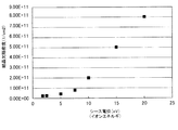
プラズマ処理時の太陽電池基板Wの表面のシース電位(イオンエネルギ)と多結晶シリコン層Snの結晶欠陥の関係を調査したところ、図7に示すようにシース電位が10eV以下の場合に、結晶欠陥の密度が2×10+11(1/cm2)以下で極めて少なくなることが確認された。本実施の形態では、シース電位を10eV以下にして低イオンエネルギでプラズマ処理を行ったので、多結晶シリコン層Snの結晶欠陥を低減し、高い光電変換効率の太陽電池を製造できる。 When the relationship between the sheath potential (ion energy) of the surface of the solar cell substrate W during the plasma treatment and the crystal defects of the polycrystalline silicon layer Sn was investigated, the crystal defects were observed when the sheath potential was 10 eV or less as shown in FIG. It was confirmed that the density was extremely low at 2 × 10 +11 (1 / cm 2 ) or less. In this embodiment, since the sheath potential is set to 10 eV or less and plasma treatment is performed with low ion energy, crystal defects in the polycrystalline silicon layer Sn are reduced, and a solar cell with high photoelectric conversion efficiency can be manufactured.
特に、マイクロ波の供給部にラジアルラインスロットアンテナ42を用いたので、プラズマがマイクロ波透過板41の直下に集中して、太陽電池基板Wの表面のシース電位を安定的に低く維持することができる。
In particular, since the radial
プラズマ処理を200℃未満で行った場合、多結晶シリコン層Snの表面に付着した水分や有機物が膜中に取り込まれることが確認された。また、プラズマ処理を600℃を超えて行った場合、多結晶シリコン層Snの再結晶化が生じてしまう。本実施の形態では、プラズマ処理を200℃〜600℃の温度下で行ったので、不純物の少ない良好な膜質のパッシベーション膜Aを形成できる。 When the plasma treatment was performed at less than 200 ° C., it was confirmed that moisture and organic substances adhering to the surface of the polycrystalline silicon layer Sn were taken into the film. Further, when the plasma treatment is performed at over 600 ° C., the polycrystalline silicon layer Sn is recrystallized. In the present embodiment, since the plasma treatment is performed at a temperature of 200 ° C. to 600 ° C., the passivation film A having a good film quality with few impurities can be formed.
図8に示すようにプラズマ処理時の処理容器30内の圧力を上げることにより、処理時のプラズマのイオンエネルギ(Ee)や電子温度(Te)を小さくできることが確認された。本実施の形態のように、処理時の処理容器30内を50mTorr(6.67Pa)以上にすることにより、低いイオンエネルギで多結晶シリコン層Snを酸化できる。この結果、多結晶シリコン層Snの結晶欠陥を低減でき、高い光電変換効率の太陽電池を製造できる。また、処理時の処理容器30内の圧力を上げすぎると、イオンエネルギが低下し過ぎてプラズマ酸化速度が著しく低下する。本実施の形態では、処理容器30内の圧力を5Torr(6.67×10²Pa)以下に維持したので、プラズマ酸化速度の著しい低下を避けることができる。
As shown in FIG. 8, it was confirmed that the ion energy (Ee) and electron temperature (Te) of plasma during processing can be reduced by increasing the pressure in the
以上の実施の形態では、処理ガスとして酸素ガスとアルゴンガスを供給していたが、処理ガスに窒素を含有させて、多結晶シリコン層Snとパッシベーション膜Aの界面の窒素原子含有率を5atomic%以下に制御してもよい。処理ガスに窒素を含有させる方法としては、処理ガスに窒素(N2)ガスやアンモニア(NH3)ガスを添加したり、処理ガスの酸素ガスの代わりにN2Oガスを用いてもよい。かかる場合、多結晶シリコン層Snの界面に窒素原子が導入されるので、多結晶シリコン層Snと酸化膜であるパッシベーション膜Aとの間の界面にできた結晶欠陥に窒素原子が選択的に反応し、窒素原子が結晶欠陥を修復する。この結果、最終的な結晶欠陥量が減少し、太陽電池の光電交換効率を上げることができる。また、図9に示すように窒素原子含有率が5atomic%を超えると、窒素原子が過剰になり、逆に多結晶シリコン層Snの界面の結晶欠陥が増加することが確認されている。したがって、窒素原子含有率を5atomic%以下にすることによって、窒素原子による結晶欠陥の修復が適正に行われる。 In the above embodiment, oxygen gas and argon gas are supplied as the processing gas. However, nitrogen is contained in the processing gas so that the nitrogen atom content at the interface between the polycrystalline silicon layer Sn and the passivation film A is 5 atomic%. You may control below. As a method for adding nitrogen to the processing gas, nitrogen (N 2 ) gas or ammonia (NH 3 ) gas may be added to the processing gas, or N 2 O gas may be used instead of the oxygen gas of the processing gas. In this case, since nitrogen atoms are introduced into the interface of the polycrystalline silicon layer Sn, the nitrogen atoms selectively react with crystal defects formed at the interface between the polycrystalline silicon layer Sn and the passivation film A that is an oxide film. Nitrogen atoms repair crystal defects. As a result, the final crystal defect amount is reduced, and the photoelectric exchange efficiency of the solar cell can be increased. In addition, as shown in FIG. 9, it has been confirmed that when the nitrogen atom content exceeds 5 atomic%, the nitrogen atoms become excessive, and conversely, crystal defects at the interface of the polycrystalline silicon layer Sn increase. Therefore, by setting the nitrogen atom content to 5 atomic% or less, the crystal defects due to nitrogen atoms are properly repaired.
以上の実施の形態では、多結晶シリコン層Snを酸化処理してパッシベーション膜Aを形成していたが、酸窒化処理してパッシベーション膜を形成してもよい。かかる場合、処理部14において、酸素ガスに代えてN2Oガスを供給してもよい。この場合も、図6に示したように従来のCVD処理の場合に比べて高い光電交換効率の太陽電池を製造できる。なお、同様に酸素ガスに代えて窒素ガスを供給して多結晶シリコン膜Snを窒化処理してパッシベーション膜を形成してもよい。
In the above embodiment, the passivation film A is formed by oxidizing the polycrystalline silicon layer Sn. However, the passivation film may be formed by oxynitriding. In such a case, the
以上の実施の形態では、処理時にプラズマを生成するマイクロ波を連続的に供給していたが、所定周期のパルス状に断続的に供給してもよい。かかる場合、例えばマイクロ波発振制御部47によって、マイクロ波発振装置46から所定周期のパルス状にマイクロ波を発振させ、ラジアルラインスロットアンテナ42から処理容器30内にパルス状のマイクロ波を供給する。例えばパルス周波数が50kHzでDuty比(ON・OFF全体の時間に対するONの時間の比)が50%になるようにマイクロ波を供給する。図10に示すように連続的なマイクロ波(連続波)を供給する場合に比べてパルス状のマイクロ波(パルス波)を供給する場合の方がプラズマのイオンエネルギを小さくできることが確認された。したがって、パルス状のマイクロ波を供給することにより、多結晶シリコン層Snとパッシベーション膜Aとの界面の欠陥を低減し、高い光電変換効率の太陽電池を製造できる。なお、この例において、パルス周波数が50kHzで、Duty比が50%であったが、パルス周波数が10kHz〜1MHzの範囲で、かつDuty比が20%〜80%の範囲であれば、連続波と比べて結晶欠陥の低減効果があることが確認された。
In the above embodiment, microwaves for generating plasma are continuously supplied at the time of processing. However, the microwaves may be intermittently supplied in a predetermined cycle. In such a case, for example, the microwave
以上の実施の形態では、例えばプラズマ酸化処理により多結晶シリコン層Snの表層にパッシベーション膜Aを形成していたが、CVD処理によりパッシベーション膜Aの上面にさらにパッシベーション膜を堆積させてもよい。 In the above embodiment, the passivation film A is formed on the surface layer of the polycrystalline silicon layer Sn by, for example, plasma oxidation processing. However, a passivation film may be further deposited on the upper surface of the passivation film A by CVD processing.
図11は、かかる一例を示すものであり、太陽電池の製造装置1は、CVD処理を行う他の処理部70、71を備えている。他の処理部70、71は、例えば上記実施の形態の処理部16、17に代えて中央搬送部10に接続されている。
FIG. 11 shows such an example, and the solar
例えば他の処理部70は、ラジアルラインスロットアンテナを用いてプラズマを発生させて、太陽電池基板Wに成膜するプラズマCVD装置である。
For example, the
他の処理部70は、例えば載置台にバイアス電力を印加するための高周波電源が接続されていることと処理ガスの種類が異なること以外は上述の処理部14と同様の構成を有している。つまり他の処理部70は、例えば図12に示すように上面が開口した有底円筒状の処理容器80を有し、その処理容器80の底部には、載置台81が設けられている。
The
載置台81には、電極板82が内蔵され、その電極板82には、直流電源83が接続されている。また、載置台81には、例えば太陽電池基板Wにバイアス電力を印加する高周波電源84が接続されている。載置台81には、ヒータ電源85による給電により発熱するヒータ86が内蔵されており、載置台81上の太陽電池基板Wを所定温度に加熱できる。
The mounting table 81 incorporates an
処理容器80の上部開口には、例えばシール材90を介して、マイクロ波透過板91が設けられている。このマイクロ波透過板91によって処理容器80内が気密に閉鎖されている。マイクロ波透過板91の上部には、ラジアルラインスロットアンテナ92が設けられている。
A
ラジアルラインスロットアンテナ92は、下面が開口した略円筒形状のケース92aを有し、その下面には、円盤状のスロット平板93が設けられている。スロット平板93には、スロットとなる多数のマイクロ波放射孔93aが形成されている。マイクロ波放射孔93aは、例えば図3に示すように隣接するもの同士がT字状に形成され、これらのT字状のマイクロ波放射孔93aが同心円状に配置されている。マイクロ波放射孔93aの長さや配列間隔は、マイクロ波の波長λに応じて定められ、例えばマイクロ波放射孔93aの間隔は、1/2λ又はλに設定されている。
The radial
スロット平板93の上部には、図12に示すように低損失誘電体材料により形成された遅相板94が設けられている。
A
ラジアルラインスロットアンテナ92のケース92aの中央部には、開口部が形成され、その開口部に同軸導波管95が接続されている。同軸導波管95は、例えば2.45GHzのマイクロ波を発振するマイクロ波発振装置96に接続されている。マイクロ波発振装置96には、マイクロ波の発振のON・OFFや出力を制御するマイクロ波発振制御部97が設けられている。
An opening is formed at the center of the
例えば処理容器80の側壁面には、処理ガス供給口100が形成されている。処理ガス供給口100には、例えば処理容器80の外部に通じる処理ガス供給管101が接続されている。処理ガス供給管101は、複数、例えば5つに分岐しており、それらの各分岐管101a、101b、101c、101d、101eは、それぞれガス供給源102a、102b、102c、102d、102eに通じている。各分岐管101a〜101eには、バルブ103a、103b、103c、103d、103e、マスフローコントローラ104a、104b、104c、104d、104eがそれぞれ設けられている。かかる構成によって、処理容器30内に所定流量の所定の処理ガスを供給することができる。本実施の形態においては、例えばガス供給源102aに、希ガスである例えばアルゴンガスが封入され、ガス供給源102bに、シラン(SiH4)ガスが封入され、ガス供給源102c、102d、102eには、N2ガス、NH3ガス、H2ガスがそれぞれ封入されている。
For example, a processing
例えば処理容器80の底部の載置台81を挟んだ両側には、排気口110が設けられている。排気口110には、ターボ分子ポンプなどの排気装置111に通じる排気管112が接続されている。この排気口110からの排気により、処理容器80内を所定の圧力に減圧できる。
For example,
次に、この例におけるパッシベーション膜の形成プロセスについて説明する。先ず、図4に示した多結晶シリコン基板Sp上に多結晶シリコン層Snが形成された太陽電池基板Wが、上記実施の形態と同様に基板搬送体8によってカセットCからアライメント部6に搬送される。その後太陽電池基板Wは、基板搬送体8によってロードロック室12に搬送され、その後基板搬送装置11によって中央搬送室10を通って例えば処理部14に搬送される。処理部14に搬送された太陽電池基板Wは、例えば上記実施の形態と同様にプラズマ処理により多結晶シリコン層Snの表層が酸化され、図13に示すように表面に第1のパッシベーション膜A1が形成される。
Next, a passivation film forming process in this example will be described. First, the solar cell substrate W in which the polycrystalline silicon layer Sn is formed on the polycrystalline silicon substrate Sp shown in FIG. 4 is transported from the cassette C to the
その後、太陽電池基板Wは、基板搬送装置11によって処理部14から取り出され、中央搬送室10を通って例えば他の処理部70に搬送される。この間、太陽電池基板Wは、大気に接しないように真空搬送される。
Thereafter, the solar cell substrate W is taken out from the
他の処理部70に搬送された太陽電池基板Wは、先ず図12に示すように載置台81上に吸着保持される。次に太陽電池基板Wは、ヒータ86によって200℃〜600℃の範囲に加熱される。続いて、処理容器80内が例えば5mTorr〜5Torrの範囲の圧力に調整され、ガス供給口100から処理容器80内に、アルゴンガス、シランガス及び窒素ガスの混合ガスが導入される。
The solar cell substrate W transported to the
続いて、ラジアルラインスロットアンテナ92から処理容器80内にマイクロ波が導入される。このマイクロ波の導入によって、処理容器80内のガスが励起して処理容器80内にプラズマが生成される。このとき、マイクロ波はスロット平板93を通過して表面波を形成し、その表面波によって、マイクロ波透過板91の直下に高密度のプラズマが生成される。また、高周波電源84により載置台81上の太陽電池基板Wに20V以上のバイアス電力が印加される。太陽電池基板Wの表面では、プラズマの作用により第1のパッシベーション膜A1の表面にシリコン窒化膜が堆積して、図14に示すように第2のパッシベーション膜A2が形成される。こうして、全体で例えば10nm以上の所定の厚みのパッシベーション膜(A1+A2)が形成される。
Subsequently, microwaves are introduced into the
所定時間のプラズマCVD処理により、所望の厚みのパッシベーション膜が形成されると、マイクロ波の供給やガスの供給が停止され、パッシベーション膜の形成処理が終了する。 When a passivation film having a desired thickness is formed by the plasma CVD process for a predetermined time, the supply of microwaves and the supply of gas are stopped, and the formation process of the passivation film ends.
その後、太陽電池基板Wは、他の処理部70から基板搬送装置11により取り出され、中央搬送室10を通ってロードロック室13に搬送される。その後太陽電池基板Wは、基板搬送体8によりカセットCに戻されて、一連の処理が終了する。
Thereafter, the solar cell substrate W is taken out from the
この例によれば、第1のパッシベーション膜A1上にCVD処理により第2のパッシベーション膜A2を形成したので、例えばプラズマ酸化処理のみではパッシベーション膜に十分な厚みが得られない場合であっても、その後のCVD処理により十分な厚みのパッシベーション膜を形成できる。この結果、パッシベーション膜が例えば反射防止膜としての機能を十分に果たすことができる。またパッシベーション膜の強度を十分に確保できる。さらに、この例では、第1のパッシベーション膜A1であるシリコン酸化膜上により反射率の高いシリコン窒化膜を形成したので、パッシベーション膜の反射防止機能をさらに向上できる。 According to this example, since the second passivation film A2 is formed on the first passivation film A1 by the CVD process, for example, even if only a plasma oxidation process cannot provide a sufficient thickness for the passivation film, A passivation film having a sufficient thickness can be formed by subsequent CVD treatment. As a result, the passivation film can sufficiently function as an antireflection film, for example. Further, the strength of the passivation film can be sufficiently secured. Furthermore, in this example, since the silicon nitride film having a higher reflectance is formed on the silicon oxide film which is the first passivation film A1, the antireflection function of the passivation film can be further improved.
また、この例にように、多結晶シリコン層Snをプラズマ酸化処理し、その上にCVD処理により窒化膜を形成してパッシベーション膜を形成した場合は、図6に示したように従来のCVD処理のみの場合や上述のプラズマ酸化処理、プラズマ窒化処理のみの場合に比べて、高い光電交換効率の太陽電池を製造できる。これは、CVD処理で形成されたシリコン窒化膜は、シリコン酸化膜より高い屈折率を持つため、プラズマ酸化処理とCVD処理を組み合わせることにより、光をパッシベーション膜内に閉じ込めやすくなって、光電変換効率が向上されるためであると考えられる。 Further, as in this example, when the polysilicon layer Sn is subjected to plasma oxidation treatment, and a passivation film is formed thereon by forming a nitride film by CVD treatment, the conventional CVD treatment is performed as shown in FIG. As compared with the case of only the above, or the case of only the above-described plasma oxidation treatment and plasma nitridation treatment, a solar cell with high photoelectric exchange efficiency can be manufactured. This is because the silicon nitride film formed by the CVD process has a higher refractive index than the silicon oxide film, so that combining the plasma oxidation process and the CVD process facilitates confinement of light in the passivation film, resulting in photoelectric conversion efficiency. Is considered to be improved.
処理部14と他の処理部70を中央搬送室10によって接続し、処理部14から他の処理部70への太陽電池基板Wの搬送を真空状態で行ったので、太陽電池基板Wが大気に曝されて例えば水分が付着して膜質が劣化することを防止できる。なお、第1のパッシベーション膜A1と第2のパッシベーション膜A2を形成する処理を同じ処理容器で行ってもよく、例えば他の処理部70の処理容器80内において、上述したプラズマ酸化処理を行って第1のパッシベーション膜A1を形成し、その後プラズマCVD処理を行って第2のパッシベーション膜A2を形成してもよい。
Since the
前記実施の形態のように第1のパッシベーション膜A1が酸化膜の場合、CVD処理時に処理ガスとして窒素ガスに加えて酸素ガスも導入し、その処理ガスの導入時に酸素に対する窒素の比率を次第に増加させて、第2のパッシベーション膜A2の窒素原子含有率を堆積方向に次第に増加させるようにしてもよい。かかる場合、例えばCVD処理時に初め酸素ガスに比べて少量の窒素ガスを導入し、その後酸素ガスの導入量を減らしつつ、窒素ガスの導入量を増加させ、最後には窒素ガスのみを導入する。こうすることにより、第2のパッシベーション膜A2の膜組成がシリコン酸化膜からシリコン窒化膜に次第に変化するので、シリコン酸化膜である第1のパッシベーション膜A1と第2のパッシベーションA2の膜組成が全体を通して連続的になる。これによってパッシベーション膜内の結晶粒界が減少し結晶欠陥を低減できる。なお、この例は、第1のパッシベーション膜A1が酸窒化膜である場合も適用できる。 When the first passivation film A1 is an oxide film as in the above embodiment, oxygen gas is also introduced in addition to nitrogen gas as a processing gas during the CVD process, and the ratio of nitrogen to oxygen is gradually increased when the processing gas is introduced. Thus, the nitrogen atom content of the second passivation film A2 may be gradually increased in the deposition direction. In such a case, for example, a small amount of nitrogen gas is first introduced compared to oxygen gas during the CVD process, and then the amount of introduced nitrogen gas is increased while reducing the amount of introduced oxygen gas, and finally only nitrogen gas is introduced. By so doing, the film composition of the second passivation film A2 gradually changes from the silicon oxide film to the silicon nitride film, so that the film composition of the first passivation film A1 and the second passivation film A2, which are silicon oxide films, is entirely increased. Become continuous through. As a result, crystal grain boundaries in the passivation film are reduced, and crystal defects can be reduced. This example can also be applied to the case where the first passivation film A1 is an oxynitride film.
なお、上記実施の形態において、CVD処理時の処理ガスにSiH4(シラン)ガスを用いていたが、これに代えてSi2H6(ジシラン)ガスなどの他のガスを用いてもよい。また、CVD処理時の処理ガスを代えることにより、第1のパッシベーション膜A1上に窒化膜に代えて酸化膜や酸窒化膜を形成してもよい。 In the above-described embodiment, SiH 4 (silane) gas is used as a processing gas at the time of CVD processing, but other gas such as Si 2 H 6 (disilane) gas may be used instead. Further, an oxide film or an oxynitride film may be formed on the first passivation film A1 instead of the nitride film by changing the processing gas during the CVD process.
以上の実施の形態で記載した、多結晶シリコン層Sn上に第1のパッシベーション膜A1を形成する処理、又は第2のパッシベーション膜A2を形成するCVD処理の少なくともいずれかにおいて、処理ガスに水素ガスを添加してもよい。かかる場合、水素原子が、パッシベーション膜中及びシリコン層とパッシベーション膜の界面中の結晶欠陥に選択的に反応して結晶欠陥を修復することができるので、より高い光電変換効率の太陽電池を製造できる。 In at least one of the process for forming the first passivation film A1 on the polycrystalline silicon layer Sn and the CVD process for forming the second passivation film A2 described in the above embodiment, a hydrogen gas is used as a process gas. May be added. In such a case, since hydrogen atoms can selectively react with crystal defects in the passivation film and at the interface between the silicon layer and the passivation film to repair the crystal defects, a solar cell with higher photoelectric conversion efficiency can be manufactured. .
以上の実施の形態で記載した処理部14〜17、他の処理部70、71は、上述のラジアルラインスロットアンテナを備えていたが、他の構造のスロットアンテナを有するものであってもよい。例えば処理部14は、図15に示すようにマイクロ波透過板41の上部に、平行平板導波路スロットアンテナ(以下、「平行平板アンテナ」とする)130を備えている。
The
平行平板アンテナ130は、平行平板導波路を形成する2枚の平板の一方にスロットが形成されたアンテナである。平行平板アンテナ130は、下側の方形の第1の導波板130aと、上側の方形の第2の導波板130bを上下に平行に対向させて備え、第1の導波板130aと第2の導波板130bの間の隙間に平行平板導波路131を形成している。第1の導波板130aには、スロットとなる多数のマイクロ波放射孔132が形成されている。マイクロ波放射孔132は、例えば図16に示すように隣接するもの同士でT字を形成し、これらのT字状のマイクロ波放射孔132が縦横に並べられて配置されている。マイクロ波放射孔132の長さや配列間隔は、平行平板導波路131内のマイクロ波の波長λに応じて定められ、例えばマイクロ波放射孔132の間隔は、λの自然数倍に設定されている。なお、マイクロ波放射孔132の形状は、T字状に限られず、円形状、円弧状等の他の形状であってもよい。また、マイクロ波放射孔132の配置は、縦横配列に限られず、同心円状、螺旋状、ランダム配置、放射状等であってもよい。
The
図15に示すように平行平板導波路131内には、誘電体からなる遅波材133が設けられている。この遅波材133によって、平行平板導波路131に導入されたマイクロ波の波長を短くしてプラズマの生成状態を調整できる。また、平行平板導波路131内の一端部には、マイクロ波吸収材134が設けられている。
As shown in FIG. 15, a
平行平板導波路131内のマイクロ波吸収材134と反対側の他端部付近には、導入されたマイクロ波を分配するマイクロ波分配部135が形成されている。そのマイクロ波分配部135には、例えば2.45GHzのマイクロ波を発振するマイクロ波発振装置136に通じる導波管137が接続されている。なお、処理部14のその他の部分の構成は、上記実施の形態で記載した処理部14の構成と同様であるので、その他の部分の構成については、上記実施の形態と同じ符号を用いて説明を省略する。
A
この処理部14によれば、マイクロ波発振装置136から発振されたマイクロ波が平行平板アンテナ130の平行平板導波路131に導入され、そのマイクロ波が第1の導波板130aのマイクロ波放射孔132を通過し、マイクロ波透過板41を通って処理容器30内に導入される。これによって、処理容器30内にマイクロ波の表面波が形成され、その表面波によって、マイクロ波透過板41の直下に高密度のプラズマが生成される。
According to the
なお、処理部15、16、17、他の処理部70、71についても、同様に平行平板アンテナ130を備えるものであってもよい。
Note that the
以上、添付図面を参照しながら本発明の好適な実施の形態について説明したが、本発明はかかる例に限定されない。当業者であれば、特許請求の範囲に記載された思想の範疇内において、各種の変更例または修正例に相到し得ることは明らかであり、それらについても当然に本発明の技術的範囲に属するものと了解される。例えば本実施の形態は、多結晶シリコン層にパッシベーション膜を形成する例であったが、単結晶、アモルファス(非晶質)、或いは多結晶とアモルファスの混在系のシリコン層にパッシベーション膜を形成する場合にも本発明は適用できる。 The preferred embodiments of the present invention have been described above with reference to the accompanying drawings, but the present invention is not limited to such examples. It will be apparent to those skilled in the art that various changes or modifications can be made within the scope of the ideas described in the claims, and these are naturally within the technical scope of the present invention. It is understood that it belongs. For example, the present embodiment is an example in which a passivation film is formed on a polycrystalline silicon layer. However, a passivation film is formed on a single crystal, amorphous (amorphous), or a mixture of polycrystalline and amorphous silicon layers. Even in this case, the present invention can be applied.
本発明は、高いエネルギ変換効率の太陽電池を製造する際に有用である。 The present invention is useful when manufacturing a solar cell with high energy conversion efficiency.
1 太陽電池の製造装置
14 処理部
42 ラジアルラインスロットアンテナ
Sp 多結晶シリコン基板
Sn 多結晶シリコン層
A パッシベーション膜
W 太陽電池基板
DESCRIPTION OF
Claims (27)
シリコン層の表層を、10eV以下のシース電位を有するプラズマを用いて酸化、窒化又は酸窒化して、前記シリコン層の表層にパッシベーション膜を形成することを特徴とする、太陽電池の製造方法。 A solar cell manufacturing method comprising:
A method for producing a solar cell, comprising oxidizing, nitriding or oxynitriding a surface layer of a silicon layer using plasma having a sheath potential of 10 eV or less to form a passivation film on the surface layer of the silicon layer.
多結晶のシリコン層とパッシベーション膜との界面における窒素原子含有率が5atomic%以下になるように、処理容器内に窒素を含む処理ガスを導入することを特徴とする、請求項1〜6のいずれかに記載の太陽電池の製造方法。 When oxidizing the surface of the polycrystalline silicon layer,
As the nitrogen atom content at the interface between the silicon layer and the passivation film of polycrystalline is below 5 atomic%, and introducing a process gas containing nitrogen into the processing chamber, any claim 1-6 A method for producing a solar cell according to claim 1.
前記CVD処理時に、処理容器内に酸素と窒素を含有する処理ガスを導入し、その導入する処理ガスの酸素に対する窒素の比率を次第に増加させて、パッシベーション膜中の窒素原子含有率を堆積方向に次第に増加させることを特徴とする、請求項8〜13のいずれかに記載の太陽電池の製造方法。 In the case of forming a passivation film by oxynitriding the surface layer of the silicon layer,
During the CVD process, a process gas containing oxygen and nitrogen is introduced into the process vessel, and the ratio of nitrogen to oxygen in the process gas to be introduced is gradually increased to increase the nitrogen atom content in the passivation film in the deposition direction. It increases gradually, The manufacturing method of the solar cell in any one of Claims 8-13 characterized by the above-mentioned.
シリコン層の表層を、10eV以下のシース電位を有するプラズマを用いて酸化、窒化又は酸窒化して、前記シリコン層の表層にパッシベーション膜を形成する処理部を有することを特徴とする、太陽電池の製造装置。 A solar cell manufacturing apparatus,
A solar cell comprising: a treatment portion that oxidizes, nitrides, or oxynitrides a surface layer of a silicon layer using a plasma having a sheath potential of 10 eV or less to form a passivation film on the surface layer of the silicon layer. Manufacturing equipment.
多結晶のシリコン層とパッシベーション膜との界面における窒素原子含有率が5atomic%以下になるように、処理容器内に窒素を含む処理ガスを導入することを特徴とする、請求項15〜20のいずれかに記載の太陽電池の製造装置。 When oxidizing the surface of the polycrystalline silicon layer,
As the nitrogen atom content at the interface between the silicon layer and the passivation film of polycrystalline is below 5 atomic%, and introducing a process gas containing nitrogen into the processing chamber, any claim 15 to 20 The manufacturing apparatus of the solar cell of crab.
前記他の処理部における前記CVD処理時に、処理容器内に酸素と窒素を含有する処理ガスを導入し、その導入する処理ガスの酸素に対する窒素の比率を次第に増加させて、パッシベーション膜中の窒素原子含有率を堆積方向に次第に増加させることを特徴とする、請求項22〜26のいずれかに記載の太陽電池の製造装置。 When forming a passivation film by oxynitriding the surface layer of the silicon layer in the processing unit,
During the CVD process in the other processing unit, a processing gas containing oxygen and nitrogen is introduced into the processing container, and the ratio of nitrogen to oxygen in the processing gas to be introduced is gradually increased to increase the nitrogen atoms in the passivation film. 27. The solar cell manufacturing apparatus according to claim 22 , wherein the content rate is gradually increased in the deposition direction.
Priority Applications (8)
| Application Number | Priority Date | Filing Date | Title |
|---|---|---|---|
| JP2006315648A JP4864661B2 (en) | 2006-11-22 | 2006-11-22 | Solar cell manufacturing method and solar cell manufacturing apparatus |
| US12/515,978 US20100029038A1 (en) | 2006-11-22 | 2007-11-06 | Manufacturing method of solar cell and manufacturing apparatus of solar cell |
| CN2007800429903A CN101542749B (en) | 2006-11-22 | 2007-11-06 | Method for manufacturing solar cell and apparatus for manufacturing solar cell |
| EP07831279A EP2096679A4 (en) | 2006-11-22 | 2007-11-06 | Method for manufacturing solar cell and apparatus for manufacturing solar cell |
| PCT/JP2007/071547 WO2008062663A1 (en) | 2006-11-22 | 2007-11-06 | Method for manufacturing solar cell and apparatus for manufacturing solar cell |
| CN2012100316452A CN102569524A (en) | 2006-11-22 | 2007-11-06 | Method for manufacturing solar cell and apparatus for manufacturing solar cell |
| KR1020097011882A KR101089130B1 (en) | 2006-11-22 | 2007-11-06 | Manufacturing method of solar cell and manufacturing apparatus of solar cell |
| TW096142731A TW200837968A (en) | 2006-11-22 | 2007-11-12 | Manufacturing method of solar battery, and manufacturing device of solar battery |
Applications Claiming Priority (1)
| Application Number | Priority Date | Filing Date | Title |
|---|---|---|---|
| JP2006315648A JP4864661B2 (en) | 2006-11-22 | 2006-11-22 | Solar cell manufacturing method and solar cell manufacturing apparatus |
Publications (2)
| Publication Number | Publication Date |
|---|---|
| JP2008130904A JP2008130904A (en) | 2008-06-05 |
| JP4864661B2 true JP4864661B2 (en) | 2012-02-01 |
Family
ID=39429601
Family Applications (1)
| Application Number | Title | Priority Date | Filing Date |
|---|---|---|---|
| JP2006315648A Expired - Fee Related JP4864661B2 (en) | 2006-11-22 | 2006-11-22 | Solar cell manufacturing method and solar cell manufacturing apparatus |
Country Status (7)
| Country | Link |
|---|---|
| US (1) | US20100029038A1 (en) |
| EP (1) | EP2096679A4 (en) |
| JP (1) | JP4864661B2 (en) |
| KR (1) | KR101089130B1 (en) |
| CN (2) | CN101542749B (en) |
| TW (1) | TW200837968A (en) |
| WO (1) | WO2008062663A1 (en) |
Families Citing this family (34)
| Publication number | Priority date | Publication date | Assignee | Title |
|---|---|---|---|---|
| UA95619C2 (en) * | 2005-12-07 | 2011-08-25 | Пфайзер Продактс Инк. | Marked bovine viral diarrhea virus vaccines |
| JP5302960B2 (en) * | 2008-06-06 | 2013-10-02 | 株式会社アルバック | Thin film solar cell manufacturing equipment |
| RU2509392C2 (en) * | 2008-08-01 | 2014-03-10 | Тел Солар Аг | Method of making photocell structure |
| EP2381483B1 (en) * | 2008-12-26 | 2014-12-10 | Ulvac, Inc. | Film-forming method |
| US8168462B2 (en) * | 2009-06-05 | 2012-05-01 | Applied Materials, Inc. | Passivation process for solar cell fabrication |
| US9166071B2 (en) * | 2009-10-27 | 2015-10-20 | Silicor Materials Inc. | Polarization resistant solar cell design using an oxygen-rich interface layer |
| CN101964378A (en) * | 2010-04-20 | 2011-02-02 | 常州天合光能有限公司 | Method for realizing graded laminated passivation film on back surface of solar cell |
| JP2012044035A (en) * | 2010-08-20 | 2012-03-01 | Hitachi High-Technologies Corp | Semiconductor manufacturing apparatus |
| CN102903785A (en) * | 2011-07-28 | 2013-01-30 | 中国科学院沈阳科学仪器研制中心有限公司 | Method for improving solar cell sheet conversion efficiency by adopting hydrogenation passivation |
| US9130093B2 (en) * | 2011-08-31 | 2015-09-08 | Alta Devices, Inc. | Method and apparatus for assembling photovoltaic cells |
| DE102011086351A1 (en) * | 2011-11-15 | 2013-05-16 | International Solar Energy Research Center Konstanz E.V. | Process for producing a solar cell with PECVD combination layer and solar cell with PECVD combination layer |
| CN104094418A (en) * | 2012-02-17 | 2014-10-08 | 应用材料公司 | Passivation film stack for silicon-based solar cells |
| DE102012101456A1 (en) | 2012-02-23 | 2013-08-29 | Schott Solar Ag | Process for producing a solar cell |
| WO2014146008A2 (en) | 2013-03-15 | 2014-09-18 | Starfire Industries Llc | Scalable multi-role surface-wave plasma generator |
| CN104064622A (en) * | 2013-03-21 | 2014-09-24 | 晶科能源有限公司 | Solar energy battery resisting potential-induced attenuation and manufacture method thereof |
| US10555412B2 (en) | 2018-05-10 | 2020-02-04 | Applied Materials, Inc. | Method of controlling ion energy distribution using a pulse generator with a current-return output stage |
| JP7043704B2 (en) * | 2018-05-23 | 2022-03-30 | 株式会社エスイー | Plasma irradiation device |
| US11476145B2 (en) | 2018-11-20 | 2022-10-18 | Applied Materials, Inc. | Automatic ESC bias compensation when using pulsed DC bias |
| CN111244223A (en) * | 2018-11-29 | 2020-06-05 | 财团法人金属工业研究发展中心 | Method for forming silicon-based laminated layer and method for manufacturing silicon-based solar cell |
| CN113169026A (en) | 2019-01-22 | 2021-07-23 | 应用材料公司 | Feedback loop for controlling pulsed voltage waveform |
| US11508554B2 (en) | 2019-01-24 | 2022-11-22 | Applied Materials, Inc. | High voltage filter assembly |
| CN110137312A (en) * | 2019-06-13 | 2019-08-16 | 天合光能股份有限公司 | A method of improving silicon nitride passivation performance |
| US11462388B2 (en) | 2020-07-31 | 2022-10-04 | Applied Materials, Inc. | Plasma processing assembly using pulsed-voltage and radio-frequency power |
| US11901157B2 (en) | 2020-11-16 | 2024-02-13 | Applied Materials, Inc. | Apparatus and methods for controlling ion energy distribution |
| US11798790B2 (en) | 2020-11-16 | 2023-10-24 | Applied Materials, Inc. | Apparatus and methods for controlling ion energy distribution |
| US11495470B1 (en) | 2021-04-16 | 2022-11-08 | Applied Materials, Inc. | Method of enhancing etching selectivity using a pulsed plasma |
| US11948780B2 (en) | 2021-05-12 | 2024-04-02 | Applied Materials, Inc. | Automatic electrostatic chuck bias compensation during plasma processing |
| US11791138B2 (en) | 2021-05-12 | 2023-10-17 | Applied Materials, Inc. | Automatic electrostatic chuck bias compensation during plasma processing |
| US11810760B2 (en) | 2021-06-16 | 2023-11-07 | Applied Materials, Inc. | Apparatus and method of ion current compensation |
| US11569066B2 (en) | 2021-06-23 | 2023-01-31 | Applied Materials, Inc. | Pulsed voltage source for plasma processing applications |
| US11776788B2 (en) | 2021-06-28 | 2023-10-03 | Applied Materials, Inc. | Pulsed voltage boost for substrate processing |
| US11476090B1 (en) | 2021-08-24 | 2022-10-18 | Applied Materials, Inc. | Voltage pulse time-domain multiplexing |
| US11694876B2 (en) | 2021-12-08 | 2023-07-04 | Applied Materials, Inc. | Apparatus and method for delivering a plurality of waveform signals during plasma processing |
| CN115404464A (en) * | 2022-09-23 | 2022-11-29 | 江苏微导纳米科技股份有限公司 | Method and apparatus for depositing thin film, and solar cell |
Family Cites Families (23)
| Publication number | Priority date | Publication date | Assignee | Title |
|---|---|---|---|---|
| US4343830A (en) * | 1980-11-13 | 1982-08-10 | Motorola, Inc. | Method for improving the efficiency of solar cells having imperfections |
| JPS58220477A (en) * | 1982-06-16 | 1983-12-22 | Japan Solar Energ Kk | Manufacture of solar battery |
| JPH0635323B2 (en) * | 1982-06-25 | 1994-05-11 | 株式会社日立製作所 | Surface treatment method |
| DE3790981T1 (en) * | 1987-07-07 | 1989-07-06 | Mobil Solar Energy Corp | METHOD FOR PRODUCING SOLAR CELLS WITH AN ANTI-REFLECTION COATING |
| JP2989923B2 (en) * | 1991-03-25 | 1999-12-13 | 京セラ株式会社 | Solar cell element |
| US5418019A (en) * | 1994-05-25 | 1995-05-23 | Georgia Tech Research Corporation | Method for low temperature plasma enhanced chemical vapor deposition (PECVD) of an oxide and nitride antireflection coating on silicon |
| JP3238003B2 (en) * | 1994-05-30 | 2001-12-10 | 京セラ株式会社 | Method of manufacturing solar cell element |
| JP4340348B2 (en) * | 1998-01-22 | 2009-10-07 | 株式会社日立国際電気 | Plasma generator |
| KR100745495B1 (en) * | 1999-03-10 | 2007-08-03 | 동경 엘렉트론 주식회사 | Semiconductor fabrication method and semiconductor fabrication equipment |
| JP4255563B2 (en) * | 1999-04-05 | 2009-04-15 | 東京エレクトロン株式会社 | Semiconductor manufacturing method and semiconductor manufacturing apparatus |
| JP3911971B2 (en) * | 1999-09-08 | 2007-05-09 | 松下電器産業株式会社 | Silicon thin film, thin film transistor, and method for manufacturing silicon thin film |
| US6323141B1 (en) * | 2000-04-03 | 2001-11-27 | Taiwan Semiconductor Manufacturing Company | Method for forming anti-reflective coating layer with enhanced film thickness uniformity |
| KR100994387B1 (en) * | 2001-01-22 | 2010-11-16 | 도쿄엘렉트론가부시키가이샤 | Method for producing material of electronic device and method for plaza processing |
| TWI225668B (en) * | 2002-05-13 | 2004-12-21 | Tokyo Electron Ltd | Substrate processing method |
| JP2004056057A (en) * | 2002-07-24 | 2004-02-19 | Sharp Corp | Manufacturing method for solar cell |
| JP4694108B2 (en) * | 2003-05-23 | 2011-06-08 | 東京エレクトロン株式会社 | Oxide film forming method, oxide film forming apparatus, and electronic device material |
| TW200511430A (en) * | 2003-05-29 | 2005-03-16 | Tokyo Electron Ltd | Plasma processing apparatus and plasma processing method |
| JP2005159171A (en) * | 2003-11-27 | 2005-06-16 | Kyocera Corp | Solar cell element and its manufacturing method |
| JP4543691B2 (en) * | 2004-02-03 | 2010-09-15 | 株式会社島津製作所 | Organic electroluminescence device and method for producing the same |
| JP4657630B2 (en) * | 2004-05-25 | 2011-03-23 | 株式会社島津製作所 | SOLAR CELL, MANUFACTURING METHOD THEREOF, AND ANTI-REFLECTION FILM DEPOSITION DEVICE |
| US7674722B2 (en) * | 2004-10-28 | 2010-03-09 | Tokyo Electron Limited | Method of forming gate insulating film, semiconductor device and computer recording medium |
| JP2006173372A (en) * | 2004-12-16 | 2006-06-29 | Shimadzu Corp | Plasma source, surface wave excitation plasma cvd device equipped therewith and depositing method |
| US20070065593A1 (en) * | 2005-09-21 | 2007-03-22 | Cory Wajda | Multi-source method and system for forming an oxide layer |
-
2006
- 2006-11-22 JP JP2006315648A patent/JP4864661B2/en not_active Expired - Fee Related
-
2007
- 2007-11-06 EP EP07831279A patent/EP2096679A4/en not_active Withdrawn
- 2007-11-06 CN CN2007800429903A patent/CN101542749B/en not_active Expired - Fee Related
- 2007-11-06 KR KR1020097011882A patent/KR101089130B1/en not_active IP Right Cessation
- 2007-11-06 WO PCT/JP2007/071547 patent/WO2008062663A1/en active Application Filing
- 2007-11-06 CN CN2012100316452A patent/CN102569524A/en active Pending
- 2007-11-06 US US12/515,978 patent/US20100029038A1/en not_active Abandoned
- 2007-11-12 TW TW096142731A patent/TW200837968A/en unknown
Also Published As
| Publication number | Publication date |
|---|---|
| KR20090085100A (en) | 2009-08-06 |
| WO2008062663A1 (en) | 2008-05-29 |
| KR101089130B1 (en) | 2011-12-02 |
| CN101542749A (en) | 2009-09-23 |
| TW200837968A (en) | 2008-09-16 |
| CN102569524A (en) | 2012-07-11 |
| EP2096679A1 (en) | 2009-09-02 |
| EP2096679A4 (en) | 2010-08-18 |
| CN101542749B (en) | 2012-04-18 |
| JP2008130904A (en) | 2008-06-05 |
| US20100029038A1 (en) | 2010-02-04 |
Similar Documents
| Publication | Publication Date | Title |
|---|---|---|
| JP4864661B2 (en) | Solar cell manufacturing method and solar cell manufacturing apparatus | |
| US6470824B2 (en) | Semiconductor manufacturing apparatus | |
| TWI450338B (en) | Method for fabricating a gate dielectric of a field effect transistor | |
| KR101760789B1 (en) | Method for depositing multi-layered layers and/or gradient layers | |
| US20130295709A1 (en) | Method for manufacturing photoelectric conversion elements | |
| US20070218687A1 (en) | Process for producing materials for electronic device | |
| EP0224360A2 (en) | Semiconductor device manufacturing method | |
| JP2001284340A (en) | Apparatus and method for manufacturing semiconductor device | |
| CN102150236A (en) | High speed thin film deposition via pre-selected intermediate | |
| JP2005005280A (en) | Method for passivating semiconductor substrate | |
| CN111172518B (en) | Integrated film coating method based on silane | |
| KR101018668B1 (en) | Method for forming silicon nano-crystalline structures terminated with oxygen or nitrogen, and silicon nano-crystalline structures terminated with oxygen or nitrogen formed thereby | |
| JP2004221427A (en) | Methods and apparatuses for manufacturing iron silicide film, photoelectric conversion element and photoelectric conversion device | |
| JP3718297B2 (en) | Thin film manufacturing method and thin film manufacturing apparatus | |
| JP2654433B2 (en) | Silicon semiconductor fabrication method | |
| JPH0766911B2 (en) | Film forming method | |
| JP2564754B2 (en) | Method for manufacturing insulated gate field effect semiconductor device | |
| JP3088703B2 (en) | Method for manufacturing thin film semiconductor device | |
| JP2009164515A (en) | Antireflection film forming method and solar cell | |
| JP2009194018A (en) | Atomic layer growth apparatus and method of growing atomic layer | |
| JP2890029B2 (en) | Film forming apparatus and film forming method | |
| KR20220058634A (en) | film formation method | |
| KR20220153262A (en) | Manufacturing method of cigs light absorption layer for solar cell using chemical vapor deposition method | |
| JPH01730A (en) | Method of forming multilayer thin film | |
| JP2012049472A (en) | Amorphous carbon and method of manufacturing the same |
Legal Events
| Date | Code | Title | Description |
|---|---|---|---|
| A131 | Notification of reasons for refusal |
Free format text: JAPANESE INTERMEDIATE CODE: A131 Effective date: 20110118 |
|
| TRDD | Decision of grant or rejection written | ||
| A01 | Written decision to grant a patent or to grant a registration (utility model) |
Free format text: JAPANESE INTERMEDIATE CODE: A01 Effective date: 20111108 |
|
| A01 | Written decision to grant a patent or to grant a registration (utility model) |
Free format text: JAPANESE INTERMEDIATE CODE: A01 |
|
| A61 | First payment of annual fees (during grant procedure) |
Free format text: JAPANESE INTERMEDIATE CODE: A61 Effective date: 20111109 |
|
| FPAY | Renewal fee payment (event date is renewal date of database) |
Free format text: PAYMENT UNTIL: 20141118 Year of fee payment: 3 |
|
| R150 | Certificate of patent or registration of utility model |
Free format text: JAPANESE INTERMEDIATE CODE: R150 |
|
| LAPS | Cancellation because of no payment of annual fees |