EP2095100B1 - Procédé de fonctionnement d'un capteur à transistor à effet de champ à nanofils - Google Patents
Procédé de fonctionnement d'un capteur à transistor à effet de champ à nanofils Download PDFInfo
- Publication number
- EP2095100B1 EP2095100B1 EP07873479.5A EP07873479A EP2095100B1 EP 2095100 B1 EP2095100 B1 EP 2095100B1 EP 07873479 A EP07873479 A EP 07873479A EP 2095100 B1 EP2095100 B1 EP 2095100B1
- Authority
- EP
- European Patent Office
- Prior art keywords
- nanoscale
- electrically conductive
- elongate structure
- nanoscale wire
- conductive elongate
- Prior art date
- Legal status (The legal status is an assumption and is not a legal conclusion. Google has not performed a legal analysis and makes no representation as to the accuracy of the status listed.)
- Not-in-force
Links
Images


Classifications
-
- G—PHYSICS
- G01—MEASURING; TESTING
- G01N—INVESTIGATING OR ANALYSING MATERIALS BY DETERMINING THEIR CHEMICAL OR PHYSICAL PROPERTIES
- G01N33/00—Investigating or analysing materials by specific methods not covered by groups G01N1/00 - G01N31/00
- G01N33/48—Biological material, e.g. blood, urine; Haemocytometers
- G01N33/50—Chemical analysis of biological material, e.g. blood, urine; Testing involving biospecific ligand binding methods; Immunological testing
- G01N33/53—Immunoassay; Biospecific binding assay; Materials therefor
- G01N33/543—Immunoassay; Biospecific binding assay; Materials therefor with an insoluble carrier for immobilising immunochemicals
- G01N33/551—Immunoassay; Biospecific binding assay; Materials therefor with an insoluble carrier for immobilising immunochemicals the carrier being inorganic
- G01N33/552—Glass or silica
-
- B—PERFORMING OPERATIONS; TRANSPORTING
- B82—NANOTECHNOLOGY
- B82Y—SPECIFIC USES OR APPLICATIONS OF NANOSTRUCTURES; MEASUREMENT OR ANALYSIS OF NANOSTRUCTURES; MANUFACTURE OR TREATMENT OF NANOSTRUCTURES
- B82Y15/00—Nanotechnology for interacting, sensing or actuating, e.g. quantum dots as markers in protein assays or molecular motors
-
- B—PERFORMING OPERATIONS; TRANSPORTING
- B82—NANOTECHNOLOGY
- B82Y—SPECIFIC USES OR APPLICATIONS OF NANOSTRUCTURES; MEASUREMENT OR ANALYSIS OF NANOSTRUCTURES; MANUFACTURE OR TREATMENT OF NANOSTRUCTURES
- B82Y30/00—Nanotechnology for materials or surface science, e.g. nanocomposites
-
- G—PHYSICS
- G01—MEASURING; TESTING
- G01N—INVESTIGATING OR ANALYSING MATERIALS BY DETERMINING THEIR CHEMICAL OR PHYSICAL PROPERTIES
- G01N27/00—Investigating or analysing materials by the use of electric, electrochemical, or magnetic means
- G01N27/26—Investigating or analysing materials by the use of electric, electrochemical, or magnetic means by investigating electrochemical variables; by using electrolysis or electrophoresis
- G01N27/403—Cells and electrode assemblies
- G01N27/414—Ion-sensitive or chemical field-effect transistors, i.e. ISFETS or CHEMFETS
- G01N27/4146—Ion-sensitive or chemical field-effect transistors, i.e. ISFETS or CHEMFETS involving nanosized elements, e.g. nanotubes, nanowires
Definitions
- the present invention generally relates to nanoscale wire methods for use in determining analytes suspected to be present in a sample.
- Nanoscopic articles might be well-suited for transport of charge carriers and excitons (e.g. electrons, electron pairs, etc.) and thus may be useful as building blocks in nanoscale electronics applications.
- Nanowires are well-suited for efficient transport of charge carriers and excitons, and thus are expected to be important building blocks for nanoscale electronics and optoelectronics.
- Nanoscale wires having selectively functionalized surfaces have been described in U.S. Patent Application Publication No. 2002/0117659 , and corresponding International Patent Application Publication WO 02/48701 .
- Nanoscale wire sensors are also described in post-published US2010/0227382 .
- functionalization of the nanoscale wire may permit interaction of the functionalized nanoscale wire with various entities, such as molecular entities, and the interaction induces a change in a property of the functionalized nanowire, which provides a mechanism for a nanoscale sensor device for detecting the presence or absence of an analyte suspected to be present in a sample.
- Various embodiments of the present invention and relevant exemplary disclosure generally relate to methods for determining analytes suspected to be present in a sample.
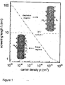
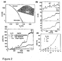
- One embodiment of the invention uses a nanoscale wire that has improved sensitivity as the carrier concentration in the wire is controlled by an external gate voltage, and in some embodiments, the nanoscale wire can be used to determine a change in charge of less than about 10 -17 C.
- the nanoscale wire is part of a field effect transistor (FET).
- the nanoscale wire has a Debye screening length that is greater than the average cross-sectional dimension of the nanoscale wire when the nanoscale wire is exposed to a solution suspected of containing an analyte.
- the Debye screening length associated with the carriers inside nanoscale wire is adjusted by adjusting the gate voltage applied to an FET structure.
- the nanoscale wire can be operated under conditions where the carriers in the nanoscale wire are depleted and the nanoscale wire has a conductance that is not linearly proportional to the voltage applied to the nanoscale wire sensor device via a gate electrode.
- the nanoscale wire may be used to determine an analyte as part of an assay for determining or diagnosing cancer or other medical conditions (e.g., by determining a suitable marker, for example, a hormone, an enzyme, a peptide, a virus, etc., and diagnosing the cancer or other medical condition based on the determination of the marker), for determining drugs (e.g., as part of a drug assay or a drug screen, for instance, to identify a drug able to treat a medical condition such as cancer or aging), for determining toxins or other environmental agents (e.g., by determining binding of the toxin to a receptor), or the like.
- a suitable marker for example, a hormone, an enzyme, a peptide, a virus, etc.
- drugs e.g., as part of a drug assay or a drug screen, for instance, to identify a drug able to treat a medical condition such as cancer or aging
- determining toxins or other environmental agents e.g
- the nanoscale wire may have a reaction entity able to interact with an analyte of interest.
- Nanoscale sensing elements of the invention may be used, for example, to determine pH or metal ions, viruses, proteins or enzymes, nucleic acids (e.g. DNA, RNA, PNA, etc.), drugs, sugars, carbohydrates, a toxin (e.g., a harmful chemical, such as a chemical produced by a living organism that is harmful to other organisms), small molecules (e.g., having molecular weights of less than about 2000 Da, less than about 1500 Da, or less than about 1000 Da), or other analytes of interest, as further described herein.
- the analyte may be charged, or uncharged in some embodiments.
- single entities may be determined, for example, a single virus, a single protein, a single enzyme, a single nucleic acid molecule, a single drug molecule, a single carbohydrate molecule, etc.
- the sensing element includes a detector constructed and arranged to determine a change in a property of the nanoscale wire, for example, a change in light emission, a change in stress or shape, or a change in an electrical property of the nanoscale wire, such as voltage, current, conductivity, resistivity, inductance, impedance, electrical change, an electromagnetic change, etc.
- the nanoscale wire is addressable by a sample (e.g., a gas or liquid sample) containing, or at least suspected of containing, the analyte.
- a sample e.g., a gas or liquid sample
- the term "addressable,” e.g., by a fluid, is defined as the ability of the fluid to be positioned relative to the nanoscale wire so that the analytes suspected of being in the fluid are able to interact with the nanoscale wire.
- the fluid may be proximate to or in contact with the nanoscale wire.
- the fluid may be directed to the nanoscale wire through the use of a microfluidic channel, as further described below.
- reaction entity refers to any entity that can interact with an analyte in such a manner as to cause a detectable change in a property of a nanoscale wire.
- the reaction entity may comprise a binding partner to which the analyte binds.
- the reaction entity when a binding partner, can comprise a specific binding partner of the analyte.
- the reaction entity can form a coating on the nanoscale wire.
- Non-limiting examples of reaction entities include a nucleic acid (e.g., DNA or RNA), an antibody, a sugar or a carbohydrate, a protein or an enzyme, a ganglioside or a surfactant, etc., e.g., as discussed herein.
- a reaction entity associated with the nanoscale wire is able to interact with an analyte.
- the reaction entity as “associated” with or “immobilize” relative to the nanoscale wire, may be positioned in relation to the nanoscale wire (e.g., in close proximity or in contact) such that the analyte can be determined by determining a change in a characteristic or property of the nanoscale wire.
- Interaction of the analyte with the reaction entity may cause a detectable change or modulation in a property of the nanoscale wire, for example, through electrical coupling with the reaction entity.
- electrically coupled when used with reference to a nanoscale wire and an analyte, or other moiety such as a reaction entity, refers to an association between any of the analyte, other moiety, and the nanoscale wire such that electrons can move from one to the other, or in which a change in an electrical characteristic of one can be determined by the other. This can include electron flow between these entities, or a change in a state of charge, oxidation, or the like, that can be determined by the nanoscale wire.
- electrical coupling or immobilization can include direct covalent linkage between the analyte or other moiety and the nanoscale wire, indirect covalent coupling (for instance, via a linker, and/or a plurality of linkers, e.g., serially), direct or indirect ionic bonding between the analyte (or other moiety) and the nanoscale wire, direct or indirect bonding of both the analyte and the nanoscale wire to a particle (i.e., the particle acts as a linker between the analyte and the nanoscale wire), direct or indirect bonding of both the analyte and the nanoscale wire to a common surface (i.e., the surface acts as a linker), or other types of bonding or interactions (e.g.
- the analyte or other moiety may simply be contacted with the nanoscale wire surface.
- the nanoscale wire is sufficiently close to the analyte to permit electron tunneling between the analyte and the nanoscale wire.
- the reaction entity may be positioned relative to the nanoscale wire to cause a detectable change in the nanoscale wire.
- the reaction entity may be positioned within about 100 nm of the nanoscale wire, within about 75 nm of the nanoscale wire, within about 50 nm of the nanoscale wire, within about 20 nm of the nanoscale wire, within about 15 nm of the nanoscale wire, or within about 10 nm of the nanoscale wire.
- the actual proximity can be determined by those of ordinary skill in the art.
- the reaction entity is positioned less than about 5 nm from the nanoscale wire.
- the reaction entity is positioned within about 4 nm, within about 3 nm, within about 2 nm, or within about 1 nm of the nanoscale wire.
- the reaction entity is fastened to or directly bonded (e.g., covalently) to the nanoscale wire, e.g., as further described herein.
- the reaction entity is not directly bonded to the nanoscale wire, but is otherwise immobilized relative to the nanoscale wire, i.e., the reaction entity is indirectly immobilized relative to the nanoscale wire.
- the reaction entity may be attached to the nanoscale wire through a linker, i.e., a species (or plurality of species) to which the reaction entity and the nanoscale wire are each immobilized relative thereto, e.g., covalently or non-covalently bound to.
- a linker may be directly bonded to the nanoscale wire, and the reaction entity may be directly bonded to the linker, or the reaction entity may not be directly bonded to the linker, but immobilized relative to the linker, e.g., through the use of non-covalent bonds such as hydrogen bonding (e.g., as in complementary nucleic acid-nucleic acid interactions), hydrophobic interactions (e.g., between hydrocarbon chains), entropic interactions, or the like.
- the linker may or may not be directly bonded (e.g., covalently) to the nanoscale wire.
- the sensitivity of the reaction entity to the analyte may be enhanced by selecting conditions in which the Debye screening length of the nanoscale wire is controlled such that the Debye screening length is greater than the average cross-sectional dimension of the nanoscale wire when the nanoscale wire is exposed to a solution suspected of containing the analyte.
- the Debye screening length can be measured by those of ordinary skill in the art (see, e.g., the examples), and varies as a function of various properties of both the nanoscale wire (e.g., the doping level and/or the dielectric constant) and the environment in which the nanoscale wire is located (e.g., the temperature of the solution).
- the Debye length of nanoscale wire is adjusted by controlling the voltage of the nanoscale wire in the gate of a FET comprising the Nanoscale wire, which changes the carrier concentration inside wire. In accordance with the invention, the Debye length is controlled to be longer than the cross-sectional dimension of the nanoscale wire.
- the screening length may be greater than the average cross-sectional dimension of the nanoscale wire.
- the ionic strength of a solution may be controlled by controlling the concentration of phosphate and/or other ions (e.g., K + , Cl - , etc.) within the solution.
- the present invention provides that the sensitivity of the reaction entity to the analyte may be enhanced under conditions where nanoscale wire has a conductance that is not linearly proportional to voltage applied to voltage applied to the nanoscale wire, i.e., within the "subthreshold regime.”
- the conductance will depend substantially exponentially on the voltage applied to the nanoscale wire, e.g., the electrolyte gate voltage if the nanoscale wire is part of an FET.
- the nanoscale wire can be used to determine a change in charge of an analyte of less than about 10 -17 C, and in some cases, less than about 5x10 -18 C, less than about 3x 10 -18 C, less than about 10 -18 C, or less than about 5x10 -19 C.
- embodiments of the present invention comprise the attachment of reaction entities, such as biological entities, to the surfaces of nanoscale wires, in some cases by using covalent bonding.
- the entity is thus immobilized with respect to the surface of the nanoscale wire.
- a linker is used to covalently immobilize the entity with respect to the nanoscale wire.
- the entity may be covalently immobilized with respect to the surface of the nanoscale wire at relatively short distances, depending on the size of the linker and/or the precursors thereof.
- the entity may be immobilized at a distance of less than about 20 nm, less than about 15 nm, less than about 10 nm, less than about 9 nm, less than about 8 nm, less than about 7 nm, less than about 6 nm, less than about 5 nm, less than about 4 nm, less than about 3 nm, less than about 2 nm, or less than about 1 nm from the surface of the nanoscale wire.
- the proximity of the entity may control or otherwise affect electronic and/or other properties of the nanoscale wire, for example, the conductivity of the nanoscale wire.
- Non-limiting examples of chemistries suitable for attaching entities to surfaces of nanoscale wires, optionally via one or more linkers include the following.
- the surface of the nanoscale wire may be functionalized, for example, the surface may be functionalized with aldehydes, amines, thiols, or the like, which may form nitrogen-containing or sulfur-containing covalent bonds.
- the reaction entity may be covalently bound to the nanoscale wire through the use of a moiety such as an aldehyde moiety, an amine moiety, and/or a thiol moiety.
- a nanoscale wire may be reacted with an aldehyde, amine, or a thiol in solution to functionalize the nanoscale wire with the appropriate moiety, e.g., such that the surface of the nanoscale wire includes terminal aldehyde, amine, and/or thiol groups. Additional examples are disclosed in US2010/027382 .
- One or more entities e.g., reaction entities such as proteins, enzymes, nucleic acids, antibodies, receptors, ligands, etc.
- reaction entities such as proteins, enzymes, nucleic acids, antibodies, receptors, ligands, etc.
- the surface of the nanoscale wire is then passivated, e.g., blocked with one or more compounds that causes the moieties to become unreactive.
- passivating agents include ethanolamine.
- a solution may be added to the nanowires that includes one or more passivating agents.
- the present invention may use a detector constructed and arranged to determine a property and/or a change in a property of the nanoscale wire.
- alteration of a property of the nanoscale wire may be indicative of an interaction between a reaction entity and an analyte (e.g., association or dissociation of the reaction entity and the analyte).
- analyte e.g., association or dissociation of the reaction entity and the analyte
- the detector will include a power source and a metering device, for example a voltmeter or an ammeter.
- a conductance (or a change in conductance) less than about 1 nS in a nanoscale wire sensor of the invention can be detected.
- a conductance in the range of thousandths of a nS can be detected.
- conductances of less than about 10 microsiemens, less than about 1 microsiemen, less than about 100 nS, or less than about 10 nS can be detected.
- concentration of a species, or analyte may be detected from femtomolar concentrations, to nanomolar, micromolar, millimolar, and to molar concentrations and above.
- a charged analyte may be determined by determining a change in an electrical property of the nanoscale wire, for example, conductivity. Immobilizing a charged analyte relative to the nanoscale wire may cause a change in the conductivity of the nanoscale wire, and in some cases, the distance between the charged analyte and the nanoscale wire may determine the magnitude of the change in conductivity of the nanoscale wire. Uncharged analytes can be similarly determined, for instance, by causing the analyte to become charged, e.g., by altering environmental conditions such as pH (by raising or lowering pH), temperature, reactants, or the like, by reacting the analyte with a charged moiety, or the like.
- sample refers to any cell, lysate, tissue, or fluid from a biological source (a "biological sample"), or any other medium, biological or non-biological, that can be evaluated in accordance with the invention.
- sample may be, for instance, a liquid (e.g., a solution or a suspension) or a gas.
- a sample includes, but is not limited to, a biological sample drawn from an organism (e.g.
- a human a non-human mammal, an invertebrate, a plant, a fungus, an algae, a bacteria, a virus, etc.
- a sample drawn from food designed for human consumption a sample including food designed for animal consumption such as livestock feed, milk, an organ donation sample, a sample of blood destined for a blood supply, a sample from a water supply, a soil sample, or the like.
- the sample is a sample suspected of containing an analyte.
- a “sample suspected of containing” a particular component means a sample with respect to which the content of the component is unknown.
- a fluid sample from a human suspected of having a disease, but not known to have the disease defines a sample suspected of containing the disease.
- Sample in this context includes naturally-occurring samples, such as physiological samples from humans or other animals, samples from food, livestock feed, water, soil, etc. Typical samples include tissue biopsies, cells, cell lysates, whole blood, serum or other blood fractions, urine, ocular fluid, saliva, fluid or other samples from tonsils, lymph nodes, needle biopsies, etc.
- sample sizes for exposure of a sample to a nanoscale sensor of the invention, can be used in various embodiments.
- the sample size used in nanoscale sensors may be less than or equal to about 10 microliters, less than or equal to about 1 microliter, or less than or equal to about 0.1 microliter.
- the sample size may be as small as about 10 nanoliters, 1 nanoliter, or less, in certain instances.
- the nanoscale sensor also allows for unique accessibility to biological species and may be used for in vivo and/or in vitro applications. When used in vivo, in some case, the nanoscale sensor and corresponding method result in a minimally invasive procedure.
- the invention uses a sensing element comprising a sample exposure region and a nanoscale wire able to detect the presence or absence of an analyte, and/or the concentration of the analyte.
- the "sample exposure region” may be any region in close proximity to the nanoscale wire where a sample in the sample exposure region addresses at least a portion of the nanoscale wire. Examples of sample exposure regions include, but are not limited to, a well, a channel, a microfluidic channel, or a gel.
- the sample exposure region is able to hold a sample proximate the nanoscale wire, and/or may direct a sample toward the nanoscale wire for determination of an analyte in the sample.
- the nanoscale wire may be positioned adjacent or within the sample exposure region.
- the nanoscale wire may be a probe that is inserted into a fluid or fluid flow path.
- the nanoscale wire probe may also comprise, in some instances, a microneedle that supports and/or is integral with the nanoscale wire, and the sample exposure region may be addressable by the microneedle.
- a device that is constructed and arranged for insertion of a microneedle probe into a sample can include a region surrounding or otherwise in contact with the microneedle that defines the sample exposure region, and a sample in the sample exposure region is addressable by the nanoscale wire, and vice versa.
- Fluid flow channels can be created at a size and scale advantageous for use in the invention (microchannels) using a variety of techniques such as those described in International Patent Application Publication No. WO 97/33737 .
- a sample such as a fluid suspected of containing an analyte that is to be determined, may be presented to a sample exposure region of a sensing element comprising a nanoscale wire.
- An analyte present in the fluid that is able to bind to the nanoscale wire and/or a reaction entity immobilized relative to the nanoscale wire may cause a change in a property of the nanoscale wire that is determinable upon binding, e.g. using conventional electronics. If the analytes is not present in the fluid, the relevant property of the nanoscale wire will remain unchanged, and the detector will measure no significant change.
- the presence or absence of an analyte can be determined by monitoring changes, or lack thereof, in the property of the nanoscale wire.
- the detector measures a change the magnitude of the change may be a function of the concentration of the analyte, and/or a function of some other relevant property of the analyte (e.g., charge or size, etc.).
- some other relevant property of the analyte e.g., charge or size, etc.
- one or more nanoscale wires may be positioned in a channel or in a microfluidic channel, which may define the sample exposure region in some cases.
- a "channel" is a conduit that is able to transport one or more fluids specifically from one location to another. Materials may flow through the channels, continuously, randomly, intermittently, etc.
- the channel may be a closed channel, or a channel that is open, for example, open to the external environment.
- the channel can include characteristics that facilitate control over fluid transport, e.g., structural characteristics, physical/chemical characteristics (e.g., hydrophobicity vs. hydrophilicity) and/or other characteristics that can exert a force (e.g., a containing force) on a fluid when within the channel.
- the fluid within the channel may partially or completely fill the channel.
- the fluid may be held or confined within the channel or a portion of the channel in some fashion, for example, using surface tension (i.e., such that the fluid is held within the channel within a meniscus, such as a concave or convex meniscus).
- the channel may have any suitable cross-sectional shape that allows for fluid transport, for example, a square channel, a circular channel, a rounded channel, a rectangular channel (e.g., having any aspect ratio), a triangular channel, an irregular channel, etc.
- the channel may be of any size.
- the channel may have a largest dimension perpendicular to a direction of fluid, flow within the channel of less than about 1000 micrometers in some cases (i.e., a inicrofluidic channel), less than about 500 micrometers in other cases, less than about 400 micrometers in other cases, less than about 300 micrometers in other cases, less than about 200 micrometers in still other cases, less than about 100 micrometers in still other cases, or less than about 50 or 25 micrometers in still other cases.
- the dimensions of the channel may be chosen such that fluid is able to freely flow through the channel.
- the dimensions of the channel may also be chosen in certain cases, for example, to allow a certain volumetric or linear flowrate of fluid within the channel.
- the number of channels, the shape or geometry of the channels, and the placement of channels can be determined by those of ordinary skill in the art.
- One or more different nanoscale wires may cross the same microfluidic channel (e.g., at different positions) to detect the same or different analytes, to measure a flowrate of an analyte(s), etc.
- one or more nanoscale wires may be positioned in a microfluidic channel to form one of a plurality of analytic elements, for instance, in a microneedle probe, a dip and read probe, etc.
- the analytic elements probe may be implantable and capable of detecting several analytes simultaneously in real time, according to certain embodiments.
- Nanoscale wires may be positioned in a microfluidic channel to form an analytic element in a microarray for a cassette or a lab-on-a-chip device.
- cassette or lab-on-a-chip devices that are suitable for high-throughout chemical analysis and screening, combinational drug discovery, etc.
- the ability to include multiple nanoscale wires in one nanoscale sensor also allows, in some cases, for the simultaneous detection of different analytes suspected of being present in a single sample, i.e., the nanoscale sensor allows "multiplexed" detection of different analytes.
- a nanoscale sensor may include a plurality of nanoscale wires that each detect different pH levels, proteins, enzymes, toxins, small molecules, and/or nucleic acids, etc.
- the sensing element may comprise a plurality of nanoscale wires able to determine (i.e., detect the presence, absence, and/or amount or concentration) one or more analytes within a sample, for example, from a liquid or solution, blood serum, etc., as previously described.
- Various nanoscale wires within the sensing element may be differentially doped as described herein, and/or contain different reaction entities, and/or the same reaction entities at different concentrations, thereby varying the sensitivity of the nanoscale wires to the analytes, as needed.
- different reaction entities may be "printed" on the nanoscale wires, e.g., using microarray printing techniques or the like, thereby producing an array of nanoscale wires comprising different reaction entities.
- individual nanoscale wires may be selected based on their ability to interact with specific analytes, thereby allowing the detection of a variety of analytes.
- the plurality of nanoscale wires may be randomly oriented or parallel to one another, according to another set of embodiments.
- the plurality of nanoscale wires may also be oriented in an array on a substrate, in specific instances.
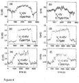
- the sensing element can collect real time data and/or near-real time data, in some embodiments. The data may be used, for example, to monitor the reaction rate of a specific chemical or biological reaction.
- Physiological conditions or drug concentrations present in vivo may also produce a real time (or near-real time) signal that may be used to control a drug delivery system, in another embodiment of the invention.
- electrical determination of one or more properties of the nanoscale wire may allow for the determination of one or more analytes as a function of time.
- the conductance of a nanoscale wire may be determined as a function of time, which may give additional information regarding the analyte.
- the nanoscale wires may be individually addressable, i.e., the status of the nanoscale wire may be determined without determining the status of nearby nanoscale wires.
- a nanoscale wire within a sensing element, or a number of nanoscale wires within the sensing element may be in electrical communication with an electrode that is able to address the nanoscale wire(s), and such a wire may be addressed using the electrode without addressing other nanoscale wires not in electrical communication with the electrode.
- a first reaction entity immobilized relative to a first nanoscale wire may bind an analyte, and such a binding event may be detectable independently of the detection of a binding event involving a second reaction entity immobilized relative to a second nanoscale wire.
- the electrodes may be in electronic communication with one or more electrical contacts.
- the invention uses a microarray including a plurality of sensing regions, at least some of which comprise one or more nanoscale wires.
- the microarray including some or all of the sensing regions, may define a sensing element in a sensor device.
- At least some of the nanoscale wires are able to determine an analyte suspected to be present in a sample that the sensing region of the microarray is exposed to, for example, the nanoscale wire may comprise a reaction entity able to interact with an analyte. If more than one nanoscale wire is present within the sensing region, the nanoscale wires may be able to detect the same analyte and/or different analytes, depending on the application.
- the invention uses a cassette comprising a sensing element having a sample exposure region and a nanoscale wire.
- the detection of an analyte in a sample within the sample exposure region may occur, in some cases, while the cassette is disconnected to a detector apparatus, allowing samples to be gathered at one site, and determined at another.
- the cassette may then be operatively connectable to a detector apparatus able to determine a property associated with the nanoscale wire.
- a device is "operatively connectable" when it has the ability to attach and interact with another apparatus.
- the cassette may be constructed and arranged such that samples may be gathered and determination at one site.
- the present invention uses, in some embodiments, an integrated system comprising a nanoscale wire detector, a reader, and a computer controlled response system.
- the nanoscale wire detects a change in the equilibrium or concentration of an analyte in the sample, feeding a signal to the computer controlled response system, causing it to withhold or release a chemical or drug.
- This is useful as an implantable drug or chemical delivery system because of its small size and low energy requirements.
- any of the techniques described herein may be used in the determination of proteins, enzymes, toxins, viruses, small molecules, or the like, e.g., as in an assay, for example, to detect or diagnose cancer or other medical conditions, toxins or other environmental agents, viruses, or the like.
- a property of an analyte may be determined by allowing the analyte to interact with a nanoscale wire and/or a reaction entity, and the interaction may be analyzed or determined in some fashion, e.g., quantified.
- the degree or amount of interaction may be determined, for example, by measuring a property of the nanoscale wire (e.g., an electronic property, such as the conductance) after exposing the nanoscale wire and/or the reaction entity to the analyte.
- a property of the nanoscale wire e.g., an electronic property, such as the conductance
- a protein, enzyme, or other target molecule may be immobilized relative to a nanoscale wire as a reaction entity, and exposed to one or more drug candidates, for example, serially or simultaneously. Interaction of the drug candidate(s) with the reaction entity may be determined by determining a property of the nanoscale wire, e.g., as previously described.
- a nanoscale wire having an associated reaction entity, may be exposed to one or more species able to interact with the reaction entity, for instance, the nanoscale wire may be exposed to a sample containing a first species able to interact with the reaction entity, where the sample contains or is suspected of containing a second species able to interact with the reaction entity, and optionally other, different species, where one of the species is a drug candidate.
- the sample may contain a substrate and a drug candidate suspected of interacting with the enzyme in a way that inhibits enzyme/substrate interaction; if the reaction entity is a substrate, the sample may contain an enzyme and a drug candidate suspected of interacting with the substrate in an inhibitory manner; if the reaction entity is a nucleic acid, the sample may contain an enzyme able to bind the nucleic acid (e.g., a nucleic acid synthesis enzyme), or a complementary nucleic acid, and a drug candidate suspected of interacting with the nucleic acid reaction entity in an inhibitory manner; if the reaction entity is a receptor, the sample may contain a ligand for the receptor and a drug candidate suspected of interacting with the receptor in an inhibitory manner; etc. In each of these cases, the drug candidate may also act in a way that enhances, rather than inhibits, interaction.
- assays of the invention may be used in high-throughput screening applications, e.g., where at least 100, at least 1,000, at least 10,000, or at least 100,000 or more analytes may be rapidly screened, for example, by exposing one or more analytes to a nanoscale wire (e.g., in solution), and/or exposing a plurality of analytes to a plurality of nanoscale wires and/or reaction entities.
- a nanoscale wire e.g., in solution
- the present invention may use a nanoscopic wire comprising one or more semiconductor and/or metal compounds, for example, for use in any of the above-described embodiments.
- the semiconductors and/or metals may be chemically and/or physically combined, for example, as in a doped nanoscopic wire.
- the nanoscopic wire may be, for example, a nanorod, a nanowire, a nanowhisker, or a nanotube.
- the nanoscopic wire may be used in a device, for example, as a semiconductor component, a pathway, etc.
- nanoscale wires and other conductors or semiconductors for use in the invention are based, in some instances, upon whether the nanoscale wire is able to interact with an analyte, or whether the appropriate reaction entity, e.g. a binding partner, can be easily attached to the surface of the nanoscale wire, or the appropriate reaction entity, e.g. a binding partner, is near the surface of the nanoscale wire.
- suitable conductors or semiconductors, including nanoscale wires will be apparent and readily reproducible by those of ordinary skill in the art with the benefit of the present disclosure.
- nanoscopic wires as used in accordance with the present invention are individual nanoscopic wires.
- "individual nanoscopic wire” means a nanoscopic wire free of contact with another nanoscopic wire (but not excluding contact of a type that may be desired between individual nanoscopic wires, e.g., as in a crossbar array).
- an "individual” or a “free-standing” article may, at some point in its life, not be attached to another article, for example, with another nanoscopic wire, or the free-standing article may be in solution.
- nanotubes produced primarily by laser vaporization techniques that produce materials formed as ropes having diameters of about 2 nm to about 50 nm or more and containing many individual nanotubes.
- conductive portions of articles which differ from surrounding material only by having been altered chemically or physically, in situ, i.e., where a portion of a uniform article is made different from its surroundings by selective doping, etching, etc.
- An "individual” or a “free-standing” article is one that can be (but need not be) removed from the location where it is made, as an individual article, and transported to a different location and combined with different components to make a functional device such as those described herein and those that would be contemplated by those of ordinary skill in the art upon reading this disclosure.
- the nanoscopic wire may include additional materials, such as semiconductor materials, dopants, organic compounds, inorganic compounds, etc.
- additional materials such as semiconductor materials, dopants, organic compounds, inorganic compounds, etc.
- the following are non-limiting examples of materials that may be used as dopants within the nanoscopic wire.
- the dopant may be an elemental semiconductor, for example, silicon, germanium, tin, selenium, tellurium, boron, diamond, or phosphorous.
- the dopant may also be a solid solution of various elemental semiconductors.
- the dopant may include mixtures of Group IV elements, for example, a mixture of silicon and carbon, or a mixture of silicon and germanium.
- the dopant may include mixtures of Group III and Group V elements, for example, BN, BP, BAs, AlN, AlP, AlAs, AlSb, GaN, GaP, GaAs, GaSb, InN, InP, InAs, or InSb.
- the dopants may include mixtures of Group III and Group V elements.
- the mixtures may include AIGaN, GaPAs, InPAs, GaInN, AlGaInN, GaInAsP, or the like.
- the dopants may also include mixtures of Group II and Group VI elements.
- the dopant may include mixtures of ZnO, ZnS, ZnSe, ZnTe, CdS, CdSe, CdTe, HgS, HgSe, HgTe, BeS, BeSe, BeTe, MgS, MgSe, or the like. Alloys or mixtures of these dopants are also be possible, for example, ZnCd Se, or ZnSSe or the like. Additionally, mixtures of different groups of semiconductors may also be possible, for example, combinations of Group II-Group VI and Group Ill-Group V elements, such as (GaAs) x (ZnS) 1-x .
- dopants may include mixtures of Group IV and Group VI elements, for example GeS, GeSe, GeTe, SnS, SnSe, SnTe, PbO, PbS, PbSe, PbTe, etc.
- Other dopant mixtures may include mixtures of Group I elements and Group VII elements, such as CuF, CuCl, CuBr, Cul, AgF, AgCl, AgBr, AgI, or the like.
- dopant mixtures may include different mixtures of these elements, such as BeSiN 2 , CaCN 2 , ZnGeP 2 , CdSnAs 2 , ZnSnSb 2 , CuGeP 3 , CuSi 2 P 3 , Si 3 N 4 , Ge 3 N 4 , Al 2 O 3 , (Al, Ga, In) 2 (S, Se, Te) 3 , Al 2 CO, (Cu, Ag)(Al, Ga, In, Tl, Fe)(S, Se, Te) 2 or the like.
- these elements such as BeSiN 2 , CaCN 2 , ZnGeP 2 , CdSnAs 2 , ZnSnSb 2 , CuGeP 3 , CuSi 2 P 3 , Si 3 N 4 , Ge 3 N 4 , Al 2 O 3 , (Al, Ga, In) 2 (S, Se, Te) 3 , Al 2 CO, (Cu, Ag)(Al, Ga, In, T
- a p-type dopant may be selected from Group III, and an n-type dopant may be selected from Group V.
- a p-type dopant may include at least one of B, Al and In, and an n-type dopant may include at least one of P, As and Sb.
- a p-type dopant may be selected from Group II, including one or more of Mg, Zn, Cd and Hg, or Group IV, including one or more of C and Si.
- An n-type dopant may be selected from at least one of Si, Ge, Sn, S, Se and Te. It will be understood that the invention is not limited to these dopants, but may include other elements, alloys, or mixtures as well.
- the term "Group,” with reference to the Periodic Table, is given its usual definition as understood by one of ordinary skill in the art.
- the Group II elements include Mg and Ca, as well as the Group II transition elements, such as Zn, Cd, and Hg.
- the Group III elements include B, Al, Ga, In and Tl;
- the Group IV elements include C, Si, Ge, Sn, and Pb;
- the Group V elements include N, P, As, Sb and Bi;
- the Group VI elements include O, S, Se, Te and Po. Combinations involving more than one element from each Group are also possible.
- a Group II-VI material may include at least one element from Group II and at least one element from Group VI, e.g., ZnS, ZnSe, ZnSSe, ZnCdS, CdS, or CdSe.
- a Group III-V material may include at least one element from Group III and at least one element from Group V, for example GaAs, GaP, GaAsP, InAs, InP, AlGaAs, or InAsP.
- Other dopants may also be included with these materials and combinations thereof, for example, transition metals such as Fe, Co, Te, Au, and the like.
- the nanoscale wire of the present invention may further include, in some cases, any organic or inorganic molecules. In some cases, the organic or inorganic molecules are polarizable and/or have multiple charge states.
- a nanoscopic wire may be a bulk-doped semiconductor.
- a "bulk-doped" article e. g. an article, or a section or region of an article
- a dopant is incorporated substantially throughout the crystalline lattice of the article, as opposed to an article in which a dopant is only incorporated in particular regions of the crystal lattice at the atomic scale, for example, only on the surface or exterior.
- some articles such as carbon nanotubes are typically doped after the base material is grown, and thus the dopant only extends a finite distance from the surface or exterior into the interior of the crystalline lattice.
- a bulk-doped semiconductor may comprise two or more bulk-doped regions.
- doped refers to bulk-doped nanoscopic wires, and, accordingly, a “doped nanoscopic (or nanoscale) wire” is a bulk-doped nanoscopic wire.
- Heavily doped and “lightly doped” are terms the meanings of which are understood by those of ordinary skill in the art.
- the invention uses a nanoscale wire (or other nanostructured material) that is a single crystal:
- a "single crystal" item e.g., a semiconductor
- Such a single-crystal item may include defects in the crystal, but is to be distinguished from an item that includes one or more crystals, not ionically or covalently bonded, but merely in close proximity to one another.
- the nanoscale wire may comprise two or more regions having different compositions.
- Each region of the nanoscale wire may have any shape or dimension, and these can be the same or different between regions.
- a region may have a smallest dimension of less than 1 micron, less than 100 nm, less than 10 nm, or less than 1 nm.
- one or more regions may be a single monolayer of atoms (i.e., "delta-doping").
- the region may be less than a single monolayer thick (for example, if some of the atoms within the monolayer are absent).
- the two or more regions may be longitudinally arranged relative to each other, and/or radially arranged (e.g., as in a core/shell arrangement) within the Nanoscale wire.
- the nanoscale wire may have multiple regions of semiconductor materials arranged longitudinally.
- a nanoscale wire may have two regions having different compositions arranged longitudinally, surrounded by a third region or several regions, each having a composition different from that of the other regions.
- the regions may be arranged in a layered structures within the nanoscale wire, and one or more of the regions may be delta-doped or at least partially delta-doped.
- the nanoscale wire may have a series of regions positioned both longitudinally and radially relative to each other.
- the arrangement can include a core that differs in composition along its length (changes in composition or concentration longitudinally), while the lateral (radial) dimensions of the core do, or do not, change over the portion of the length differing in composition.
- the shell portions can be adjacent each other (contacting each other, or defining a change in composition or concentration of a unitary shell structure longitudinally), or can be separated from each other by, for example, air, an insulator, a fluid, or an auxiliary, non-nanoscale wire component.
- the shell portions can be positioned directly on the core, or can be separated from the core by one or more intermediate shells portions that can themselves be constant in composition longitudinally, or varying in composition longitudinally, i.e., the invention allows the provision of any combination of a nanowire, core and any number of radially-positioned shells (e.g., concentric shells), where the core and/or any shells can vary in composition and/or concentration longitudinally, any shell sections can be spaced from any other shell sections longitudinally, and different numbers of shells can be provided at different locations longitudinally along the structure.
- a nanoscale wire may be positioned proximate the surface of a substrate, i.e., the nanoscale wire may be positioned within about 50 nm, about 25 nm, about 10 nm, or about 5 nm of the substrate. In some cases, the proximate nanoscale wire may contact at least a portion of the substrate.
- the substrate comprises a semiconductor and/or a metal. Non-limiting examples include Si, Ge, GaAs, etc. Other suitable semiconductors and/or metals are described above with reference to nanoscale wires.
- the substrate may comprise a nonmetal/nonsemiconductor material, for example, a glass, a plastic or a polymer, a gel, a thin film, etc.
- a nonmetal/nonsemiconductor material for example, a glass, a plastic or a polymer, a gel, a thin film, etc.
- suitable polymers include polyethylene, polypropylene, poly(ethylene terephthalate), polydimethylsiloxane, or the like.
- a method of preparing a nanosclale wire may involve allowing a first material to diffuse into at least part of a second material, optionally creating a new compound.
- the first and second materials may each be metals or semiconductors, one material may be a metal and the other material may be a semiconductor, such that a semiconductor may be annealed to a metal.
- a portion of the semiconductor and/or a portion of the metal may be heated such that at least some metal atoms are able to diffuse into the semiconductor, or vice versa.
- a metal electrode e.g., a nickel, gold, copper, silver, chromium electrode, etc.
- a metal electrode may be positioned in physical contact with a semiconductor nanoscopic wire, and then annealed such that at least a portion of the semiconductor diffuses into at least a portion of the metal, optionally forming a metal-semiconductor compound, e.g., as disclosed in International Patent Application Publication WO2005/033831 .
- the semiconductor may be annealed with the metal at a temperature of about 300 °C, about 350 °C, about 400 °C, about 450 °C, about 500 °C, about 550 °C, or about 600 °C for a period of time of at least about 30 minutes, at least about 1 hour, at least about 2 hours, at least about 4 hours, at least about 6 hours etc.
- annealing may allow, for example, lower contact resistances or impedances between the metal and the semiconductor.
- the metal may be passivated, e.g., as described herein.
- the metal, or at least a portion of the metal may be exposed to one or more passivating agents, for example, Si 3 N 4 . Insulation of the metal by the passivating agent may be used to form a layer covering the surface of the metal, for example, to prevent reaction or nonspecific binding between an analyte and the metal.
- a metal electrode may be in electrical communication with a semiconductor comprising one or more immobilized reaction entities, and the metal electrode may be passivated to prevent a reaction or nonspecific binding between the metal and the reaction entity, and/or to reduce or prevent leakage current from the metal.
- the passivation may be conducted at a relatively high temperature, for example, within a plasma CVD chamber.
- the method of preparation may also involve controlling and altering the doping of semiconductors in a nanoscale wire.
- the nanoscale wires (or other nanostructure) may be produced using techniques that allow for direct and controlled growth of the nanoscale wires.
- the nanoscale wire may be doped during growth of the nanoscale wire. Doping the nanoscale wire during growth may result in the property that the doped nanoscale wire is bulk-doped.
- doped nanoscale wires may be controllably doped, such that a concentration of a dopant within the doped nanoscale wire can be controlled and therefore reproduced consistently.
- Nanoscopic wires may also be grown through laser catalytic growth.
- LCG metal-catalyzed CVD techniques
- nanoscale wires with uniform size (diameter) distribution can be produced, where the diameter of the wires is determined by the size of the catalytic clusters.
- Nanoscale Wires may be doped by introducing the doping element into the vapor phase reactant (e.g. diborane and phosphane).
- the doping concentration may be controlled by controlling the relative amount of the doping compound introduced in the composite target.
- the final doping concentration or ratios are not necessarily the same as the vapor-phase concentration or ratios.
- LCG laser catalytic growth
- a desired material e.g. silicon or indium phosphide
- a catalytic material e.g. a nanoparticle catalyst
- the vapor may condense into liquid nanoclusters through collision with a buffer gas. Growth may begin when the liquid nanoclusters become supersaturated with the desired phase and can continue as long as reactant is available. Growth may terminate when the nanoscale wire passes out of the hot reaction zone and/or when the temperature is decreased.
- the nanoscale wire may be further subjected to different semiconductor reagents during growth.
- nanoscale wires of any of a variety of materials may be grown directly from vapor phase through a vapor-solid process.
- nanoscale wires may also be produced by deposition on the edge of surface steps, or other types of patterned surfaces.
- nanoscale wires may be grown by vapor deposition in or on any generally elongated template.
- the porous membrane may be porous silicon, anodic alumina, a diblock copolymer, or any other similar structure.
- the natural fiber may be DNA molecules, protein molecules carbon nanotubes, any other elongated structures.
- the source materials may be a solution or a vapor.
- the template may also include be column micelles formed by surfactant.
- the nanoscale wire may be doped after formation.
- a nanoscale wire having a substantially homogeneous composition is first synthesized, then is doped post-synthetically with various dopants. Such doping may occur throughout the entire nanoscale wire, or in one or more portions of the nanoscale wire, for example, in a wire having multiple regions differing in composition.
- the method of preparing a sensor device may involve the assembly, or controlled placement, of nanoscale wires on a surface.
- Any substrate may be used for nanoscale wire placement, for example, a substrate comprising a semiconductor, a substrate comprising a metal, a substrate comprising a glass, a substrate comprising a polymer, a substrate comprising a gel, a substrate that is a thin film, a substantially transparent substrate, a non-planar substrate, a flexible substrate, a curved substrate, etc.
- assembly can be carried out by aligning nanoscale wires using an electrical field.
- assembly can be performed using an arrangement involving positioning a fluid flow directing apparatus to direct fluid containing suspended nanoscale wires toward and in the direction of alignment with locations at which nanoscale wires are desirably positioned.
- a nanoscale wire is formed on the surface of a substrate, and/or is defined by a feature on a substrate.
- a nanoscale wire is formed as follows.
- a substrate is imprinted using a stamp or other applicator to define a pattern, such as a nanoscale wire or other nanoscale structure.
- the imprintable layer is removed, for example, through etching processes such as reactive ion etching (RIE), or other known techniques.
- RIE reactive ion etching
- enough imprintable material may be removed from the substrate so as to expose portions of the substrate free of the imprintable material.
- a metal or other materials may then be deposited onto at least a portion of the substrate, for example, gold, copper, silver, chromium, etc.
- a "lift-off" step may then be performed, where at least a portion of the imprintable material is removed from the substrate.
- Metal or other material deposited onto the imprintable material may be removed along with the removal of the imprintable material, for example, to form one or more nanoscale wires. Structures deposited on the surface may be connected to one or more electrodes in some cases.
- the substrate may be any suitable substrate that can support an imprintable layer, for example, comprising a semiconductor, a metal, a glass, a polymer, a gel, etc.
- the substrate may be a thin film, substantially transparent, non-planar, flexible, and/or curved, etc.
- an array of nanoscale wires may be produced by providing a surface having a plurality of substantially aligned nanoscale wires, and removing, from the surface, a portion of one or more of the plurality of nanoscale wires. The remaining nanoscale wires on the surface may then be connected to one or more electrodes.
- the nanoscopic wires are arranged such that they are in contact with each other; in other instances, however, the aligned nanoscopic wires may be at a pitch such that they are substantially not in physical contact.
- nanoscale wires are positioned proximate a surface using flow techniques, i.e., techniques where one or more nanoscale wires may be carried by a fluid to a substrate.
- Nanoscale wires (or any other elongated structures) can be aligned by inducing a flow of a nanoscale wire solution on surface, where the flow can include channel flow or flow by any other suitable technique.
- Nanoscale wire arrays with controlled position and periodicity can be produced by patterning a surface of a substrate and/or conditioning the surface of the nanoscale wires with different functionalities, where the position and periodicity control may be achieved by designing specific complementary forces between the patterned surface and the nanoscale wires.
- Nanoscale wires can also be assembled using a Langmuir-Blodgett (LB) trough. Nanoscale wires may first be surface-conditioned and dispersed to the surface of a liquid phase to form a Langmuir-Blodgett film.
- the liquid may include a surfactant, which can, in some cases, reduce aggregation of the nanoscale wires and/or reduce the ability of the nanoscale wires to interact with each other.
- the nanoscale wires can be aligned into different patterns (such as parallel arrays or fibers) by compressing the surface or reducing the surface area of the surface.
- Another arrangement involves forming surfaces on a substrate including regions that selectively attract nanoscale wires surrounded by regions that do not selectively attract them.
- Surfaces can be patterned using known techniques such as electron-beam patterning, "soft-lithography” such as that described in International Patent Application Publication No. WO 96/29629 ; or U.S. Patent No. 5,512,131 , entitled “Formation of Microstamped Patterns on Surfaces and Derivative Articles,” issued April 30,1996. Additional techniques are described in WO 01/03208 .
- Fluid flow channels can be created at a size scale advantageous for placement of nanoscale wires on surfaces using a variety of techniques such as those described in International Patent Application Publication No. WO 97/33737 .
- Other techniques include those described in U.S. Patent No. 6,645,432 , entitled “Microfluidic Systems Including Three-dimensionally Arrayed Channel Networks,” issued November 11, 2003.
- Chemically patterned surfaces other than SAM-derivatized surfaces can be used, and many techniques for chemically patterning surfaces are known.
- Another example of a chemically patterned surface may be a micro-phase separated block copolymer structure. These structures may provide a stack of dense lamellar phases, where a cut through these phases reveals a series of "lanes" wherein each lane represents a single layer.
- the assembly of nanoscale wires onto substrate and electrodes can also be assisted using bimolecular recognition in some cases.
- one biological binding partner may be immobilized onto the nanoscale wire surface and the other one onto a substrate or an electrode using physical adsorption or covalently linking.
- SAMs self-assembled monolayers.
- Any of a variety of substrates and SAM-forming material can be used along with microcontact printing techniques, such as those described in International Patent Application. Publication No. WO 96/29629 .
- the nanoscale wire arrays may also be transferred to another substrate, e.g., by using stamping techniques.
- nanoscale wires may be assembled using complementary interaction, i.e., where one or more complementary chemical, biological, electrostatic, magnetic or optical interactions are used to position one or more nanoscale wires on a substrate.
- physical patterns may be used to position nanoscale wires proximate a surface.
- nanoscale wires may be positioned on a substrate using physical patterns, for instance, aligning the nanoscale wires using comer of the surface steps or along trenches on the substrate.
- the present invention uses at least one of the above-mentioned devices packaged in kits, optionally including instructions for use of the devices.
- instructions can define a component of instructional utility (e.g., directions, guides, warnings, labels, notes, FAQs ("frequently asked questions"), etc., and typically involve written instructions on or associated with packaging of the invention.
- Instructions can also include instructional communications in any form (e.g., oral, electronic, digital, optical, visual, etc.), provided in any manner such that a user will clearly recognize that the instructions are to be associated with the device, e.g., as discussed herein.
- the kit may include other components depending on the specific application, for example, containers, adapters, syringes, needles, replacement parts, etc.
- Certain embodiments of the invention may include wires or other components of scale commensurate with nanometer-scale wires, which includes nanotubes and nanowires. In some embodiments, however, the invention also provides articles that may be greater than nanometer size (e. g., micrometer-sized).
- nanometer size e. g., micrometer-sized.
- “nanoscopic-scale,” “nanoscopic,” “nanometer-scale,” “nanoscale,” the “nano-” prefix (for example, as in “nanostructured”), and the like generally refers to elements or articles having widths or diameters of less than about 1 micron, and less than about 100 nm in some cases.
- specified widths can be a smallest width (i.e. a width as specified where, at that location, the article can have a larger width in a different dimension), or a largest width (i.e. where, at that location, the article has a width that is no wider than as specified, but can have a length that is greater).
- a "wire” generally refers to any material having a conductivity of or of similar magnitude to any semiconductor or any metal, and in some embodiments may be used to connect two electronic components such that they are in electronic communication with each other.
- the terms “electrically conductive” or a “conductor” or an “electrical conductor” when used with reference to a “conducting" wire or a nanoscale wire refers to the ability of that wire to pass charge.
- an electrically conductive nanoscale wire will have a resistivity comparable to that of metal or semiconductor materials, and in some cases, the electrically conductive nanoscale wire may have lower resistivities, for example, resistivities of less than about 100 microOhm cm ( ⁇ cm).
- the electrically conductive nanoscale wire will have a resistivity lower than about 10 -3 ohm meters, lower than about 10 -4 ohm meters, or lower than about 10 -6 ohm meters or 10 -7 ohm meters.
- a "semiconductor,” as used herein, is given its ordinary meaning in the art, i.e., an element having semiconductive or semi-metallic properties (i.e., between metallic and non-metallic properties).
- An example of a semiconductor is silicon.
- Other non-limiting examples include gallium, germanium, diamond (carbon), tin, selenium, tellurium, boron, or phosphorous.
- a “nanoscopic wire” (also known herein as a “nanoscopic-scale wire” or “nanoscale wire”) generally is a wire, that at any point along its length, has at least one cross-sectional dimension and, in some embodiments, two orthogonal cross-sectional dimensions less than 1 micron, less than about 500 nm, less than about 200 nm, less than about 150 nm, less than about 100 nm, less than about 70, less than about 50 nm, less than about 20 nm, less than about 10 nm, or less than about 5 nm. In other embodiments, the cross-sectional dimension can be less than 2 nm or 1 nm.
- the nanoscale wire has at least one cross-sectional dimension ranging from 0.5 nm to 100 nm or 200 nm.
- the nanoscale wire is electrically conductive.
- the cross-section of a nanoscopic wire may be of any arbitrary shape, including, but not limited to, circular, square, rectangular, annular, polygonal, or elliptical, and may be a regular or an irregular shape.
- the nanoscale wire may be solid or hollow. A non-limiting list of examples of materials from which nanoscale wires of the invention can be made appears below.
- any nanoscale wire can be used in any of the embodiments described herein, including carbon nanotubes, molecular wires (i.e., wires formed of a single molecule), nanorods, nanowires, nanowhiskers, organic or inorganic conductive or semiconducting polymers, and the like, unless otherwise specified.
- Other conductive or semiconducting elements that may not be molecular wires, but are of various small nanoscopic-scale dimensions, can also be used in some instances, e.g. inorganic structures such as main group and metal atom-based wire-like silicon, transition metal-containing wires, gallium arsenide, gallium nitride, indium phosphide, germanium, cadmium selenide, etc.
- nanoscale wires can be grown on and/or applied to surfaces in patterns useful for electronic devices in a manner similar to techniques described herein involving the specific nanoscale wires used as examples, without undue experimentation.
- the nanoscale wires may be formed having dimensions of at least about 1 micron, at least about 3 microns, at least about 5 microns, or at least about 10 microns or about 20 microns in length, and can be less than about 100 nm, less than about 80 nm, less than about 60 nm, less than about 40 nm, less than about 20 nm, less than about 10 nm, or less than about 5 nm in thickness (height and width).
- the nanoscale wires may have an aspect ratio (length to thickness) of greater than about 2:1, greater than about 3:1, greater than about 4:1, greater than about 5:1, greater than about 10:1, greater than about 25:1, greater than about 50:1, greater than about 75:1, greater than about 100:1, greater than about 150:1, greater than about 250:1, greater than about 500:1, greater than about 750:1, or greater than about 1000:1 or more in some cases.
- a “nanowire” (e. g. comprising silicon and/or another semiconductor material) is a nanoscopic wire that is typically a solid wire, and may be elongated in some cases.
- a nanowire (which is abbreviated herein as "NW”) is an elongated semiconductor, i.e., a nanoscale semiconductor.
- a “non-nanotube nanowire” is any nanowire that is not a nanotube.
- a non-nanotube nanowire having an unmodified surface (not including an auxiliary reaction entity not inherent in the nanotube in the environment in which it is positioned) is used in any arrangement of the invention described herein in which a nanowire or nanotube can be used.
- a “nanotube” e.g. a carbon nanotube
- NT nanotube
- Nanotubes are used as one example of small wires for use in the invention and, in certain embodiments, devices of the invention include wires of scale commensurate with nanotubes.
- Examples of nanotubes that may be used in the present invention include, but are not limited to, single-walled nanotubes (SWNTs). Structurally, SWNTs are formed of a single graphene sheet rolled into a seamless tube.
- SWNTs single-walled nanotubes
- SWNTs can behave as one-dimensional metals and/or semiconductors.
- SWNTs can behave as one-dimensional metals and/or semiconductors.
- Methods of manufacture of nanotubes, including SWNTs, and characterization are known.
- Methods of selective functionalization on the ends and/or sides of nanotubes also are known, and the present invention makes use of these capabilities for molecular electronics in certain embodiments.
- Multi-walled nanotubes are well known, and can be used as well.
- an "elongated" article e.g. a semiconductor or a section thereof
- an "elongated" article is an article for which, at any point along the longitudinal axis of the article, the ratio of the length of the article to the largest width at that point is greater than 2:1.
- a “width” of an article is the distance of a straight line from a point on a perimeter of the article, through the center of the article, to another point on the perimeter of the article.
- a “width” or a “cross-sectional dimension" at a point along a longitudinal axis of an article is the distance along a straight line that passes through the center of a cross-section of the article at that point and connects two points on the perimeter of the cross-section.
- the "cross-section" at a point along the longitudinal axis of an article is a plane at that point that crosses the article and is orthogonal to the longitudinal axis of the article.
- the "longitudinal axis" of an article is the axis along the largest dimension of the article.
- a “longitudinal section” of an article is a portion of the article along the longitudinal axis of the article that can have any length greater than zero and less than or equal to the length of the article.
- the "length" of an elongated article is a distance along the longitudinal axis from end to end of the article.
- a "cylindrical" article is an article having an exterior shaped like a cylinder, but does not define or reflect any properties regarding the interior of the article.
- a cylindrical article may have a solid interior, may have a hollowed-out interior, etc.
- a cross-section of a cylindrical article appears to be circular or approximately circular, but other cross-sectional shapes are also possible, such as a hexagonal shape.
- the cross-section may have any arbitrary shape, including, but not limited to, square, rectangular, or elliptical. Regular and irregular shapes are also included.
- an "array" of articles comprises a plurality of the articles, for example, a series of aligned nanoscale wires, which may or may not be in contact with each other.
- a "crossed array” or a “crossbar array” is an array where at least one of the articles contacts either another of the articles or a signal node (e.g., an electrode).
- the invention uses a nanoscale wire or wires forming part of a system constructed and arranged to determine an analyte in a sample to which the nanoscale wire(s) is exposed.
- “Determine,” in this context, generally refers to the analysis of a species, for example, quantitatively or qualitatively, and/or the detection of the presence or absence of the species. “Determining” may also refer to the analysis of an interaction between two or more species, for example, quantitatively or qualitatively, and/or by detecting the presence or absence of the interaction, e.g. determination of the binding between two species.
- an analyte may cause a determinable change in an electrical property of a nanoscale wire (e.g., electrical conductivity, resistivity, impedance, etc.), a change in an optical property of the nanoscale wire, etc.
- determination techniques include, but are not limited to, piezoelectric measurement, electrochemical measurement, electromagnetic measurement, photodetection, mechanical measurement, acoustic measurement, gravimetric measurement, and the like. "Determining" also means detecting or quantifying interaction between species.
- a "fluid,” as used herein, generally refers to a substance that tends to flow and to conform to the outline of its container.
- fluids are materials that are unable to withstand a static shear stress. When a shear stress is applied to a fluid, it experiences a continuing and permanent distortion.
- Typical fluids include liquids and gases, but may also include free-flowing solid particles, viscoelastic fluids, and the like.
- a component that is "immobilized relative to" another component either is fastened to the other component or is indirectly fastened to the other component, e.g., by being fastened to a third component to which the other component also is fastened.
- a first entity is immobilized relative to a second entity if a species fastened to the surface of the first entity attaches to an entity, and a species on the surface of the second entity attaches to the same entity, where the entity can be a single entity, a complex entity of multiple species, another particle, etc.
- a component that is immobilized relative to another component is immobilized using bonds that are stable, for example, in solution or suspension.
- non-specific binding of a component to another component, where the components may easily separate due to solvent or thermal effects is not preferred.
- fastened to or adapted to be fastened to means that the species and/or surfaces are chemically or biochemically linked to or adapted to be linked to, respectively, each other via covalent attachment, attachment via specific biological binding (e.g., biotin/streptavidin), coordinative bonding such as chelate/metal binding, or the like.
- specific biological binding e.g., biotin/streptavidin
- coordinative bonding such as chelate/metal binding, or the like.
- fastened in this context includes multiple chemical linkages, multiple chemical/biological linkages, etc., including, but not limited to, a binding species such as a peptide synthesized on a nanoscale wire, a binding species specifically biologically coupled to an antibody which is bound to a protein such as protein A, which is attached to a nanoscale wire, a binding species that forms a part of a molecule, which in turn is specifically biologically bound to a binding partner covalently fastened to a surface of a nanoscale wire, etc.
- a species also is adapted to be fastened to a surface if a surface carries a particular nucleotide sequence, and the species includes a complementary nucleotide sequence.
- Specifically fastened or “adapted to be specifically fastened” means a species is chemically or biochemically linked to or adapted to be linked to, respectively, another specimen or to a surface as described above with respect to the definition of "fastened to or adapted to be fastened,” but excluding essentially all non-specific binding.
- Covalently fastened means fastened via essentially nothing other than one or more covalent bonds.
- binding refers to the interaction between a corresponding pair of molecules or surfaces that exhibit mutual affinity or binding capacity, typically due to specific or non-specific binding or interaction, including, but not limited to, biochemical, physiological, and/or chemical interactions.
- Biological binding defines a type of interaction that occurs between pairs of molecules including proteins, nucleic acids, glycoproteins, carbohydrates, hormones and the like.
- Non-limiting examples include antibody/antigen, antibody/hapten, enzyme/substrate, enzyme/inhibitor, enzyme/cofactor, binding protein/substrate, carrier protein/substrate, lectin/carbohydrate, receptor/hormone, receptor/effector, complementary strands of nucleic acid, protein/nucleic acid repressor/inducer, ligand/cell surface receptor, virus/ligand, virus/cell surface receptor, etc.
- binding partner refers to a molecule that can undergo binding with a particular molecule.
- Biological binding partners are examples.
- Protein A is a binding partner of the biological molecule IgG, and vice versa.
- Other non-limiting examples include nucleic acid-nucleic acid binding, nucleic acid-protein binding, protein-protein binding, enzyme-substrate binding, receptor-ligand binding, receptor-hormone binding, antibody-antigen binding, etc.
- Binding partners include specific, semi-specific, and non-specific binding partners as known to those of ordinary skill in the art.
- Protein A is usually regarded as a "non-specific" or semi-specific binder.
- binding partner e.g., protein, nucleic acid, antibody, etc.
- a binding partner e.g., protein, nucleic acid, antibody, etc.
- a reaction that is determinative of the presence and/or identity of one or other member of the binding pair in a mixture of heterogeneous molecules (e.g., proteins and other biologics).
- heterogeneous molecules e.g., proteins and other biologics.
- An enzyme would specifically bind to its substrate, a nucleic acid would specifically bind to its complement, an antibody would specifically bind to its antigen.
- nucleic acids that specifically bind (hybridize) to their complement include nucleic acids that specifically bind (hybridize) to their complement, antibodies specifically bind to their antigen, binding pairs such as those described above, and the like.
- the binding may be by one or more of a variety of mechanisms including, but not limited to ionic interactions, and/or covalent interactions, and/or hydrophobic interactions, and/or van der Waals interactions, etc.
- polypeptide polypeptide
- peptide protein
- protein protein
- amino acid polymers in which one or more amino acid residue is an artificial chemical analogue of a corresponding naturally occurring amino acid, as well as to naturally occurring amino acid polymers.
- amino acid polymers in which one or more amino acid residue is an artificial chemical analogue of a corresponding naturally occurring amino acid, as well as to naturally occurring amino acid polymers.
- the term also includes variants on the traditional peptide linkage joining the amino acids making up the polypeptide.
- polynucleotide or “oligonucleotide” or grammatical equivalents generally refer to a polymer of at least two nucleotide bases covalently linked together, which may include, for example, but not limited to, natural nucleosides (e.g., adenosine, thymidine, guanosine, cytidine, uridine, deoxyadenosine, deoxythymidine, deoxyguanosine and deoxycytidine), nucleoside analogs (e.g., 2-aminoadenosine, 2-thiothymidine, inosine, pyrrolopyrimidine, 3-methyladenosine, C5-bromouridine, C5-fluorouridine, C5-iodouridine, C5-propynyluridine, C5-propynylcytidine, C5-methylcytidine, 7-deazaaden
- oligonucleotide is a polymer having 20 bases or less
- polynucleotide is a polymer having at least 20 bases.
- nucleic acid is given its ordinary meaning as used in the art. Nucleic acids can be single-stranded or double stranded, and will generally contain phosphodiester bonds, although in some cases, as outlined below, nucleic acid analogs are included that may have alternate backbones, comprising, for example, phosphoramide ( Beaucage et al. (1993) Tetrahedron 49(10):1925 ) and references therein; Letsinger (1970) J. Org. Chem. 35:3800 ; SRocl et al. (1977) Eur. J Biochem. 81: 579 ; Letsinger et al. (1986) Nucl. Acids Res.
- an “antibody” refers to a protein or glycoprotein including one or more polypeptides substantially encoded by immunoglobulin genes or fragments of immunoglobulin genes.
- the recognized immunoglobulin genes include the kappa, lambda, alpha, gamma, delta, epsilon and mu constant region genes, as well as myriad immunoglobulin variable region genes.
- Light chains are classified as either kappa or lambda.
- Heavy chains are classified as gamma, mu, alpha, delta, or epsilon, which in turn define the immunoglobulin classes, IgG, IgM, IgA, IgD and IgE, respectively.
- a typical immunoglobulin (antibody) structural unit is known to comprise a tetramer.
- Each tetramer is composed of two identical pairs of polypeptide chains, each pair having one "light” (about 25 kD) and one "heavy” chain (about 50-70 kD).
- the N-terminus of each chain defines a variable region of about 100 to 110 or more amino acids primarily responsible for antigen recognition.
- the terms variable light chain (VL) and variable heavy chain (VH) refer to these light and heavy chains respectively.
- Antibodies exist as intact immunoglobulins or as a number of well characterized fragments produced by digestion with various peptidases. Thus, for example, pepsin digests an antibody below (i.e.
- the F(ab)'2 may be reduced under mild conditions to break the disulfide linkage in the hinge region thereby converting the (Fab')2 dimer into an Fab' monomer.
- the Fab' monomer is essentially a Fab with part of the hinge region (see, Paul (1993) Fundamental Immunology, Raven Press, N.Y . for a more detailed description of other antibody fragments).
- Preferred antibodies include single chain antibodies, e.g., single chain Fv (scFv) antibodies in which a variable heavy and a variable light chain are joined together (directly or through a peptide linker) to form a continuous polypeptide.
- scFv single chain Fv
- quantum dot is known to those of ordinary skill in the art, and generally refers to semiconductor or metal nanoparticles that absorb light and quickly re-emit light in a different color depending on the size of the dot. For example, a 2 nanometer quantum dot emits green light, while a 5 nanometer quantum dot emits red light. Cadmium selenide quantum dot nanocrystals are available from Quantum Dot Corporation of Hayward, California.
- the sensitivity of a nanowire (NW) field effect transistor (FET) sensor is shown to be enhanced in the low carrier concentration regime where the screening length is longer than the radius of the nanowire, and therefore the molecules bound on surface can gate the whole cross-section of nanowire.
- NW nanowire
- FET field effect transistor
- This example also shows that optimization of a nanowire FET structure and operating conditions can provide a significant enhancement of, as well as a fundamental understanding for, the sensitivity of a NW-FET sensor.
- operating in the subthreshold regime was shown in this example to improve the prostate specific antigen (PSA) detection limit down to ⁇ 1.5 fM for a NW-FET sensor with a -0.75 pM detection limit in the linear regime.
- PSA prostate specific antigen
- the sensing mechanism is the field gating effect of charged molecules on the carrier conduction inside NW. Therefore, the highest sensitivity may be achieved when the whole volume of nanodevice is gated by surface charges. This situation may be realized when the carrier screening length is much larger than the radius of the NW, R.
- Conductance changes of NW FETs can be used to detect pH, proteins, and viruses, for example, as is discussed in US2010/0227382 .
- Si-NWs used for sensor application often have R on the order of 100 nm, or 10 nm in some cases.
- charged molecules bound on the surface gate the NW within a surface layer of thickness ⁇ 1-2 nm.
- p e.g., lower than 10 18 /cm 3
- ⁇ Si >> R and the whole volume of the NW may be gated by molecules at surface.
- FIG. 1 A schematic comparison between these two scenarios is shown in Fig. 1 , together with the screening length in silicon plotted as a function of p .
- This figure shows the screening length effect on the operation and sensitivity of NW FET sensors.
- the working regime and effectiveness of gating effect induced by molecules at the surface of the NW-FET sensors were determined by the relative magnitude between carrier screening length ⁇ Si and nanowire size (radius) R .
- ⁇ Si ⁇ R carrier screening length
- R nanowire size
- the amount of band bending at the NW surface is also denoted as surface potential shift ⁇ Si .
- carriers in the NW may have long screening length ( ⁇ Si >> r ) and the field effect of surface charges can gate the whole NW, fully utilizing the high surface volume ratio of NW.
- the Fermi level E F is shifted by ⁇ Si , relative to the band edges throughout the whole cross-section of NW.
- ⁇ G the conductance change of device
- ⁇ G / G the conductance change of device
- pH sensing experiments were used as a model system to study the sensitivity of NW sensor in the various regimes. Following are nanowire FET fabrication and surface modification for sensing experiments procedures.
- Nanowire FET fabrication and electrolyte gating were performed as follows. Silicon nanowires were synthesized by chemical vapor deposition using 10 nm gold nanoparticles as catalysts, with silane as the reactant. Diborane was used during the growth to provide boron as the p-type dopant with a typical B:Si ratio of 1:8000. The FETs were fabricated by photolithography into a patterned array. Nickel (60 nm thick) metal was used as contacts which were passivated/protected from electrolyte by deposition of ⁇ 50 nm thick Si 3 N 4 after nickel evaporation. The distance between the source-drain electrodes for each FET was 2 ⁇ m.
- pH and PSA samples were delivered to the nanowire devices by a microfluidic channel (with a 500 ⁇ m width by 50 ⁇ m height cross-section) made of flexible PDMS polymer channel sealed to the device chip.
- the samples were delivered through inlet/outlet connections in the PDMS polymer by a syringe pump running at typical speed of 0.3 ml/hr.
- a gold metal pad (without Si 3 N 4 passivation) on the chip was used as a global gate electrode for gating all the devices in electrolyte.
- the FET conductance was measured by a lock-in amplifier at a frequency of 17 Hz an biased voltage of 30 mV.
- Nanowire surface modifications were performed as follows. For pH sensing, the silicon nanowire surface was modified with 3-aminopropyltriethoxysilane (3APTS) to provide amino groups at the nanowire surface. The chip was first reacted with 1% 3APTS in ethanol for ⁇ 30 min. Then the chip was rinsed with ethanol and baked at 110 °C for 5-10 min before conductance measurements. For PSA sensing (see below), a two-step modification process was used to link antibody receptors to nanowire.
- 3APTS 3-aminopropyltriethoxysilane
- the silicon oxide (SiO 2 ) surface of boron doped p-type Si-NW was modified with 3-aminopropyltriethoxysilane.
- the protonation/deprotonation of amino (-NH 2 ) and silanol (Si-OH) groups changes the surface charge and surface potential of the NW when the pH of electrolyte solution was varied.
- a gold pad on the chip was used as a gate electrode to gate the NW-FET devices in the electrolyte (inset, Fig. 2A).
- Fig. 2A shows the conductance G vs. the electrolyte gate voltage V g of a p-type NW FET.
- the inset shows a schematic diagram of electrolyte gating. This device has a transconductance ⁇ 700 nS/V in the linear regime and a subthreshold slope S ⁇ 180 mV/decade in the subthreshold regime, with a threshold voltage V T ⁇ 0 V.
- the parameter characterizing the FET performance in the subthreshold regime was the subthreshold slope S , which equals the change in V g needed to tune the device conductance G by a factor of about ten.
- S the gate coupling efficiency
- ⁇ the gate coupling efficiency
- a transconductance g m d G /d V g ⁇ 700 nS/V was determined at V g less than the threshold voltage V T ( ⁇ 0 V for this device), where G depended on V g linearly (the "linear regime" ofFET).
- the device shows much larger percentage change in conductance as solution pH changes.
- the upper and lower lines in this figure are exponential and linear responses for pH induced surface potential shift of -30 mV/pH. Since in experiments, the potential at the SiO 2 surface was measured instead of the potential at the Si/SiO 2 interface ofNW, the data were analyzed in terms of ⁇ SiO2 , the surface potential at the SiO 2 /electrolyte interface.
- g m 700 nS/V obtained from the G ( V g ) data in electrolyte-gating measurement
- ⁇ SiO2 ⁇ -30 mV/pH was obtained.
- the negative sign comes from the fact that the SiO 2 surface is more negatively charged at higher pH.
- the pH sensing data were analyzed in the subthreshold regime according to the analysis on the NW sensor response in the ⁇ Si >> R regime.
- the pH sensitivity in terms of surface potential of materials had a theoretical limit of 60 mV/pH, which is set by the Nernst equation. Depending on site densities and the dissociation constants of functional groups on the material surface, the measured ⁇ (pH) may be lower than the ideal 60 mV/pH.
- C NW e 2 d p /d E F .
- C ⁇ C ox +C DL C ⁇ C DL .
- Table 1 shows that it is possible to detect charge as little as several e using a NW FET sensor working in the subthreshold regime and low ionic strength electrolyte. Besides demonstrating, in this example, the capability of NW FET devices as sensitive charge sensors, these quantitative determinations also provide a fundamental understandings for charge sensitivity of a nanosensor made from quasi-1D materials.
- NW sensors can also be used in high throughout sensitive detection of complex biomolecules such as proteins.
- This example is a demonstration of biomolecule detection in the subthreshold regime of the NW sensor for a cancer marker protein, prostate specific antigen (PSA).
- PSA detection a p-type Si-NW surface was first modified with aldehyde propyltrimethoxysilane, which provides aldehyde groups at NW surface. The aldehyde terminated NW surface was then covalently linked with PSA antibodies, which act as receptors to detect the PSA molecules in analyte solutions, as shown in Fig. 3A , which is a schematic of the PSA/PSA-Ab binding/unbinding equilibrium system.
- Fig. 3B presents data on detecting 15 pM PSA at different electrolyte gate voltage V g .
- the increased conductance between the arrows was caused by the binding of negatively charged PSA molecules on the p-type NW surface.
- the sensor performance may also be relatively optimized (in terms of the highest ⁇ G/G and signal to noise ratio) in the subthreshold regime, consistent with the above discussion based on the screening length effect on the sensitivity as well as the pH sensing experiments.
- the curves show a minimal PSA detection limit ⁇ 0.75 pM for this device in the linear regime.
- Fig. 5 shows the potential distribution ⁇ ( r ) inside silicon nanowire at different ratios between the nanowire radius R and the carrier screening length ⁇ Si .
- ⁇ ( r ) is normalized by its value at surface.
- R limit is consistent with the well known compressibility of a non-degenerate electron gas, and remains valid for 1D after replacing p ⁇ R 2 with the 1D charge density (which can be shown to be true by calculating the exact density dependence of the chemical potential of 1D Fermions at finite temperatures).
- the screening length of silicon enters C NW in the expression at the ⁇ Si ⁇ R limit accounts for the fact that the chemical potential of carriers in NW only changes inside a layer of thickness ⁇ ⁇ Si nearby its surface.
- a reference to "A and/or B", when used in conjunction with open-ended language such as “comprising” can refer, in one embodiment, to A only (optionally including elements other than B); in another embodiment, to B only (optionally including elements other than A); in yet another embodiment, to both A and B (optionally including other elements); etc.
- the phrase "at least one,” in reference to a list of one or more elements, should be understood to mean at least one element selected from any one or more of the elements in the list of elements, but not necessarily including at least one of each and every element specifically listed within the list of elements and not excluding any combinations of elements in the list of elements.
- This definition also allows that elements may optionally be present other than the elements specifically identified within the list of elements to which the phrase "at least one" refers, whether related or unrelated to those elements specifically identified.
- At least one of A and B can refer, in one embodiment, to at least one, optionally including more than one, A, with no B present (and optionally including elements other than B); in another embodiment, to at least one, optionally including more than one, B, with no A present (and optionally including elements other than A); in yet another embodiment, to at least one, optionally including more than one, A, and at least one, optionally including more than one, B (and optionally including other elements); etc.
Claims (26)
- Procédé permettant de déterminer si un échantillon suspecté de contenir un analyte le contient, comprenant l'étape consistant à :fournir un transistor à effet de champ, le transistor à effet de champ comprenant :une structure allongée électriquement conductrice, ladite structure allongée électriquement conductrice ayant une largeur ou un diamètre inférieur à environ 1 micron, la structure allongée électriquement conductrice ayant une entité de réaction immobilisée relativement à celle-ci capable d'interagir avec l'analyte, au moins une partie de ladite structure allongée électriquement conductrice pouvant être adressée par l'échantillon ; etune électrode de grille pour portillonner la structure allongée électriquement conductrice,caractérisé en ce que le procédé comprend en outre l'étape consistant à ajuster la tension de l'électrode de grille de sorte que ladite structure allongée électriquement conductrice ait une longueur de passage Debye dans l'échantillon qui soit supérieure à la dimension en coupe transversale moyenne de ladite structure allongée électriquement conductrice,la longueur de passage Debye étant définie par

- Procédé selon la revendication 1, dans lequel l'entité de réaction comprend un acide nucléique.
- Procédé selon la revendication 1, dans lequel l'entité de réaction comprend une protéine.
- Procédé selon la revendication 1, dans lequel l'entité de réaction comprend une enzyme.
- Procédé selon la revendication 1, dans lequel l'entité de réaction comprend un anticorps.
- Procédé selon la revendication 1, dans lequel l'entité de réaction est immobilisée de manière covalente relativement à la structure allongée électriquement conductrice.
- Procédé selon la revendication 1, dans lequel l'entité de réaction est immobilisée relativement à la structure allongée électriquement conductrice par le biais d'un lieur.
- Procédé selon la revendication 1, dans lequel l'entité de réaction est positionnée sur 5 nanomètres de la structure allongée électriquement conductrice.
- Procédé selon la revendication 8, dans lequel l'entité de réaction est positionnée sur 3 nanomètres de la structure allongée électriquement conductrice.
- Procédé selon la revendication 9, dans lequel l'entité de réaction est positionnée sur 1 nanomètre de la structure allongée électriquement conductrice.
- Procédé selon la revendication 1, dans lequel la structure allongée électriquement conductrice est un nanofil à semi-conducteur.
- Procédé selon la revendication 11, dans lequel le nanofil à semiconducteur est un nanofil de silicium.
- Procédé selon la revendication 1, dans lequel l'entité de réaction se lie spécifiquement à l'analyte.
- Procédé selon la revendication 1, dans lequel l'entité de réaction se lie de manière non-spécifique à l'analyte.
- Procédé selon la revendication 1, dans lequel la solution échantillon a une force ionique inférieure à environ 10 mM.
- Procédé selon la revendication 15, dans lequel la solution échantillon a une force ionique inférieure à environ 3 mM.
- Procédé selon la revendication 16, dans lequel la solution échantillon a une force ionique inférieure à environ 1 mM.
- Procédé selon la revendication 17, dans lequel la solution échantillon a une force ionique inférieure à environ 300 micromolaires.
- Procédé selon la revendication 18, dans lequel la solution échantillon a une force ionique inférieure à environ 100 micromolaires.
- Procédé selon la revendication 19, dans lequel la solution échantillon a une force ionique inférieure à environ 30 micromolaires.
- Procédé selon la revendication 20, dans lequel la solution échantillon a une force ionique inférieure à environ 10 micromolaires.
- Procédé selon l'une quelconque des revendications précédentes, comprenant en outre les étapes consistant à fournir un détecteur construit et agencé pour déterminer une propriété associée à la structure allongée électriquement conductrice.
- Procédé selon la revendication 22, dans lequel le détecteur est construit et agencé pour déterminer une propriété électrique associée à la structure allongée électriquement conductrice.
- Procédé selon la revendication 22, dans lequel le détecteur est construit et agencé pour déterminer un changement d'une propriété électromagnétique associée à la structure allongée électriquement conductrice.
- Procédé selon l'une quelconque des revendications précédentes, dans lequel le transistor à effet de champ est ménagé dans une zone de détection d'une biopuce.
- Procédé selon l'une quelconque des revendications précédentes, comprenant en outre les étapes consistant à :exposer le transistor à effet de champ à une solution échantillon suspectée de contenir un analyte avec lequel l'entité de réaction peut interagir, etdéterminer un changement d'une propriété de la structure allongée électriquement conductrice au moyen du détecteur.
Applications Claiming Priority (2)
| Application Number | Priority Date | Filing Date | Title |
|---|---|---|---|
| US86058606P | 2006-11-22 | 2006-11-22 | |
| PCT/US2007/024126 WO2008127314A1 (fr) | 2006-11-22 | 2007-11-19 | Capteurs à nanofil à haute sensibilité |
Publications (2)
| Publication Number | Publication Date |
|---|---|
| EP2095100A1 EP2095100A1 (fr) | 2009-09-02 |
| EP2095100B1 true EP2095100B1 (fr) | 2016-09-21 |
Family
ID=39758418
Family Applications (1)
| Application Number | Title | Priority Date | Filing Date |
|---|---|---|---|
| EP07873479.5A Not-in-force EP2095100B1 (fr) | 2006-11-22 | 2007-11-19 | Procédé de fonctionnement d'un capteur à transistor à effet de champ à nanofils |
Country Status (3)
| Country | Link |
|---|---|
| US (2) | US8575663B2 (fr) |
| EP (1) | EP2095100B1 (fr) |
| WO (1) | WO2008127314A1 (fr) |
Families Citing this family (36)
| Publication number | Priority date | Publication date | Assignee | Title |
|---|---|---|---|---|
| EP2360298A3 (fr) | 2000-08-22 | 2011-10-05 | President and Fellows of Harvard College | Proédé pour le dépot d'un nano-fil semiconducteur |
| AU2904602A (en) | 2000-12-11 | 2002-06-24 | Harvard College | Nanosensors |
| US20100227382A1 (en) | 2005-05-25 | 2010-09-09 | President And Fellows Of Harvard College | Nanoscale sensors |
| WO2006132659A2 (fr) | 2005-06-06 | 2006-12-14 | President And Fellows Of Harvard College | Heterostructures nanofils |
| EP2013611A2 (fr) * | 2006-03-15 | 2009-01-14 | The President and Fellows of Harvard College | Nanobioélectronique |
| EP2035584B1 (fr) | 2006-06-12 | 2011-01-26 | President and Fellows of Harvard College | Nano-capteurs et technologies associees |
| US8058640B2 (en) | 2006-09-11 | 2011-11-15 | President And Fellows Of Harvard College | Branched nanoscale wires |
| US8575663B2 (en) | 2006-11-22 | 2013-11-05 | President And Fellows Of Harvard College | High-sensitivity nanoscale wire sensors |
| CA2701380C (fr) * | 2007-10-01 | 2014-03-11 | University Of Southern California | Detection d'adn methyle et de mutations d'adn |
| CN102150037B (zh) * | 2008-07-11 | 2014-06-04 | 康奈尔大学 | 集成电荷传感器的纳米流体通道及基于该纳米流体通道的方法 |
| US20100204062A1 (en) * | 2008-11-07 | 2010-08-12 | University Of Southern California | Calibration methods for multiplexed sensor arrays |
| US8421072B2 (en) * | 2008-11-12 | 2013-04-16 | Alcatel Lucent | Electronic device having thermally managed electron path and method of thermal management of very cold electrons |
| US20100256344A1 (en) * | 2009-04-03 | 2010-10-07 | University Of Southern California | Surface modification of nanosensor platforms to increase sensitivity and reproducibility |
| US9297796B2 (en) | 2009-09-24 | 2016-03-29 | President And Fellows Of Harvard College | Bent nanowires and related probing of species |
| EP2617069B1 (fr) * | 2010-09-14 | 2014-12-03 | Commissariat à l'Énergie Atomique et aux Énergies Alternatives | Dispositif optoélectronique à base de nanofils pour l'émission de lumière |
| US8399262B2 (en) | 2011-03-23 | 2013-03-19 | Darrel A. Mazzari | Biosensor |
| US20120272721A1 (en) * | 2011-04-28 | 2012-11-01 | Stichting Imec Nederland | Device comprising a gas sensor sensitive to the presence of a specific gas, method of manufacturing a gas sensor sensitive to the presence of a specific gas for use in the device and use of the device |
| WO2012170630A2 (fr) * | 2011-06-10 | 2012-12-13 | President And Fellows Of Harvard College | Fils d'échelle nanométrique, dispositifs de transistor à effet de champ à fil d'échelle nanométrique, et dispositifs hybrides nanotube-électronique pour détection et autres applications |
| WO2013166259A1 (fr) | 2012-05-03 | 2013-11-07 | President And Fellows Of Harvard College | Capteurs à l'échelle nanoscopique pour applications intracellulaires et autres |
| US20170054858A1 (en) | 2012-09-12 | 2017-02-23 | Fabricio COELHO | System and method for sharing collaborative digital photo albums |
| EP2909601B1 (fr) | 2012-10-16 | 2019-09-11 | Abbott Laboratories | Procédé et appareil pour agrandir la longueur de debye à une surface d'un capteur dans un échantillon liquide et support de mémoire correspondant lisible par un ordinateur |
| KR101414131B1 (ko) | 2013-01-21 | 2014-07-01 | 한국표준과학연구원 | 전류 소자 및 이를 이용한 전자 펌핑 방법 |
| EP3158330B1 (fr) * | 2014-06-19 | 2019-03-06 | The Board of Trustees of The Leland Stanford Junior University | Appareils et procédés pour la détermination d'une charge d'analyte |
| US10782285B2 (en) | 2014-10-03 | 2020-09-22 | Rite Taste, LLC | Device and method for chemical analysis |
| US9664674B2 (en) | 2014-10-03 | 2017-05-30 | Rite Taste, LLC | Device and method for chemical analysis |
| US10105080B1 (en) | 2014-10-24 | 2018-10-23 | Verily Life Sciences Llc | Interstitial fluid sampling above microneedle array |
| US9666748B2 (en) | 2015-01-14 | 2017-05-30 | International Business Machines Corporation | Integrated on chip detector and zero waveguide module structure for use in DNA sequencing |
| US20190309349A1 (en) * | 2016-05-18 | 2019-10-10 | Integrated Nano-Technologies, Inc. | Method for detection of a pcr product |
| US10444179B2 (en) | 2016-08-10 | 2019-10-15 | Multerra Bio, Inc. | Apparatuses and methods for detecting molecules and binding energy |
| US9816988B1 (en) | 2016-08-10 | 2017-11-14 | Multerra Bio, Inc. | Apparatuses and methods for detecting molecules and binding energy |
| JP2019526332A (ja) * | 2016-08-22 | 2019-09-19 | ラモット・アット・テル・アビブ・ユニバーシテイ・リミテッドRamot At Tel Aviv University Ltd. | 皮下検知のための方法およびシステム |
| KR20190040010A (ko) | 2016-08-22 | 2019-04-16 | 라모트 앳 텔-아비브 유니버시티 리미티드 | 생분석물 검출을 위한 방법 및 시스템 |
| US11715772B1 (en) * | 2016-08-30 | 2023-08-01 | Femtodx, Inc. | Field-controlled sensor architecture and related methods |
| US11209416B2 (en) | 2017-07-28 | 2021-12-28 | Graphene-Dx, Inc. | Device and method for chemical analysis |
| WO2019148167A1 (fr) | 2018-01-29 | 2019-08-01 | Rite Taste, LLC | Procédés et dispositifs pour la détection de pathogènes |
| US11056602B2 (en) | 2019-06-20 | 2021-07-06 | United States Of America As Represented By The Secretary Of The Navy | Device, system, and method for selectively tuning nanoparticles with graphene |
Family Cites Families (249)
| Publication number | Priority date | Publication date | Assignee | Title |
|---|---|---|---|---|
| US905586A (en) | 1908-03-14 | 1908-12-01 | Mcloughlin Brothers | Disk propeller or game apparatus. |
| US3873359A (en) * | 1971-11-26 | 1975-03-25 | Western Electric Co | Method of depositing a metal on a surface of a substrate |
| US3873360A (en) * | 1971-11-26 | 1975-03-25 | Western Electric Co | Method of depositing a metal on a surface of a substrate |
| US3900614A (en) | 1971-11-26 | 1975-08-19 | Western Electric Co | Method of depositing a metal on a surface of a substrate |
| US4341009A (en) | 1980-12-05 | 1982-07-27 | International Business Machines Corporation | Method for making an electrical contact to a silicon substrate through a relatively thin layer of silicon dioxide on the surface of the substrate |
| US6846654B1 (en) | 1983-11-29 | 2005-01-25 | Igen International, Inc. | Catalytic antibodies as chemical sensors |
| JPS6194042A (ja) * | 1984-10-16 | 1986-05-12 | Matsushita Electric Ind Co Ltd | 分子構築体およびその製造方法 |
| US4939556A (en) | 1986-07-10 | 1990-07-03 | Canon Kabushiki Kaisha | Conductor device |
| US5089545A (en) * | 1989-02-12 | 1992-02-18 | Biotech International, Inc. | Switching and memory elements from polyamino acids and the method of their assembly |
| US5023139A (en) * | 1989-04-04 | 1991-06-11 | Research Corporation Technologies, Inc. | Nonlinear optical materials |
| JPH05501928A (ja) | 1989-10-18 | 1993-04-08 | リサーチ コーポレーション テクノロジーズ インコーポレーテッド | 被覆した粒子及び粒子の被覆の方法 |
| US5332910A (en) | 1991-03-22 | 1994-07-26 | Hitachi, Ltd. | Semiconductor optical device with nanowhiskers |
| US5274602A (en) | 1991-10-22 | 1993-12-28 | Florida Atlantic University | Large capacity solid-state memory |
| JP3243303B2 (ja) * | 1991-10-28 | 2002-01-07 | ゼロックス・コーポレーション | 量子閉じ込め半導体発光素子及びその製造方法 |
| US5475341A (en) | 1992-06-01 | 1995-12-12 | Yale University | Sub-nanoscale electronic systems and devices |
| US5252835A (en) | 1992-07-17 | 1993-10-12 | President And Trustees Of Harvard College | Machining oxide thin-films with an atomic force microscope: pattern and object formation on the nanometer scale |
| EP0622439A1 (fr) | 1993-04-20 | 1994-11-02 | Koninklijke Philips Electronics N.V. | Particules semiconductrices dopées par un activateur à l'échelle du quantum |
| US5453970A (en) | 1993-07-13 | 1995-09-26 | Rust; Thomas F. | Molecular memory medium and molecular memory disk drive for storing information using a tunnelling probe |
| AU8070294A (en) | 1993-07-15 | 1995-02-13 | President And Fellows Of Harvard College | Extended nitride material comprising beta -c3n4 |
| US5512131A (en) * | 1993-10-04 | 1996-04-30 | President And Fellows Of Harvard College | Formation of microstamped patterns on surfaces and derivative articles |
| US5900160A (en) * | 1993-10-04 | 1999-05-04 | President And Fellows Of Harvard College | Methods of etching articles via microcontact printing |
| US6180239B1 (en) * | 1993-10-04 | 2001-01-30 | President And Fellows Of Harvard College | Microcontact printing on surfaces and derivative articles |
| US5776748A (en) | 1993-10-04 | 1998-07-07 | President And Fellows Of Harvard College | Method of formation of microstamped patterns on plates for adhesion of cells and other biological materials, devices and uses therefor |
| US5936703A (en) | 1993-10-13 | 1999-08-10 | Nof Corporation | Alkoxysilane compound, surface processing solution and contact lens |
| JP3254865B2 (ja) | 1993-12-17 | 2002-02-12 | ソニー株式会社 | カメラ装置 |
| EP0659911A1 (fr) | 1993-12-23 | 1995-06-28 | International Business Machines Corporation | Procédé pour la formation d'un film polycristallin sur un substrat |
| US5599677A (en) | 1993-12-29 | 1997-02-04 | Abbott Laboratories | Immunoassays for prostate specific antigen |
| JP3460096B2 (ja) | 1994-05-30 | 2003-10-27 | 富士通株式会社 | 半導体装置の製造方法 |
| US5620850A (en) * | 1994-09-26 | 1997-04-15 | President And Fellows Of Harvard College | Molecular recognition at surfaces derivatized with self-assembled monolayers |
| WO1996014206A1 (fr) * | 1994-11-08 | 1996-05-17 | Spectra Science Corporation | Substances d'affichage constituees de nanocristaux semi-conducteurs et dispositif d'affichage faisant appel a ces substances |
| US5581091A (en) | 1994-12-01 | 1996-12-03 | Moskovits; Martin | Nanoelectric devices |
| US5866434A (en) | 1994-12-08 | 1999-02-02 | Meso Scale Technology | Graphitic nanotubes in luminescence assays |
| US5539214A (en) | 1995-02-06 | 1996-07-23 | Regents Of The University Of California | Quantum bridges fabricated by selective etching of superlattice structures |
| US5524092A (en) * | 1995-02-17 | 1996-06-04 | Park; Jea K. | Multilayered ferroelectric-semiconductor memory-device |
| EP0812434B1 (fr) | 1995-03-01 | 2013-09-18 | President and Fellows of Harvard College | Procede d'impression par microcontact sur des surfaces et articles obtenus par ce procede |
| CA2213854C (fr) | 1995-03-10 | 2010-08-10 | Meso Scale Technologies, Llc | Essai par electrochimioluminescence multispecifique et multirangee |
| US5747180A (en) * | 1995-05-19 | 1998-05-05 | University Of Notre Dame Du Lac | Electrochemical synthesis of quasi-periodic quantum dot and nanostructure arrays |
| US5824470A (en) | 1995-05-30 | 1998-10-20 | California Institute Of Technology | Method of preparing probes for sensing and manipulating microscopic environments and structures |
| US5751156A (en) * | 1995-06-07 | 1998-05-12 | Yale University | Mechanically controllable break transducer |
| US6190634B1 (en) * | 1995-06-07 | 2001-02-20 | President And Fellows Of Harvard College | Carbide nanomaterials |
| US5757038A (en) * | 1995-11-06 | 1998-05-26 | International Business Machines Corporation | Self-aligned dual gate MOSFET with an ultranarrow channel |
| WO1997019208A1 (fr) * | 1995-11-22 | 1997-05-29 | Northwestern University | Procede d'encapsulation d'un materiau dans un nanotube en carbone |
| JP2904090B2 (ja) | 1996-01-10 | 1999-06-14 | 日本電気株式会社 | 単一電子素子 |
| US6036774A (en) * | 1996-02-26 | 2000-03-14 | President And Fellows Of Harvard College | Method of producing metal oxide nanorods |
| US5897945A (en) * | 1996-02-26 | 1999-04-27 | President And Fellows Of Harvard College | Metal oxide nanorods |
| AU724277B2 (en) | 1996-03-06 | 2000-09-14 | Hyperion Catalysis International, Inc. | Functionalised nanotubes |
| DE19610115C2 (de) | 1996-03-14 | 2000-11-23 | Fraunhofer Ges Forschung | Detektion von Molekülen und Molekülkomplexen |
| AU723909B2 (en) | 1996-03-15 | 2000-09-07 | President And Fellows Of Harvard College | Method of forming articles and patterning surfaces via capillary micromolding |
| US6355198B1 (en) * | 1996-03-15 | 2002-03-12 | President And Fellows Of Harvard College | Method of forming articles including waveguides via capillary micromolding and microtransfer molding |
| US6060121A (en) * | 1996-03-15 | 2000-05-09 | President And Fellows Of Harvard College | Microcontact printing of catalytic colloids |
| US5640343A (en) * | 1996-03-18 | 1997-06-17 | International Business Machines Corporation | Magnetic memory array using magnetic tunnel junction devices in the memory cells |
| RU2099808C1 (ru) | 1996-04-01 | 1997-12-20 | Евгений Инвиевич Гиваргизов | Способ выращивания ориентированных систем нитевидных кристаллов и устройство для его осуществления (варианты) |
| US5942443A (en) | 1996-06-28 | 1999-08-24 | Caliper Technologies Corporation | High throughput screening assay systems in microscale fluidic devices |
| JPH09298284A (ja) * | 1996-05-09 | 1997-11-18 | Nec Corp | 半導体容量素子の形成方法 |
| US5726524A (en) * | 1996-05-31 | 1998-03-10 | Minnesota Mining And Manufacturing Company | Field emission device having nanostructured emitters |
| JP2000516708A (ja) | 1996-08-08 | 2000-12-12 | ウィリアム・マーシュ・ライス・ユニバーシティ | ナノチューブ組立体から作製された巨視的操作可能なナノ規模の装置 |
| US6118492A (en) * | 1996-08-14 | 2000-09-12 | Starsight Telecast, Inc. | Guide system and method of operation |
| JPH10106960A (ja) | 1996-09-25 | 1998-04-24 | Sony Corp | 量子細線の製造方法 |
| JP3858319B2 (ja) | 1996-12-05 | 2006-12-13 | ソニー株式会社 | 量子細線の製造方法 |
| US6038060A (en) * | 1997-01-16 | 2000-03-14 | Crowley; Robert Joseph | Optical antenna array for harmonic generation, mixing and signal amplification |
| US5908692A (en) * | 1997-01-23 | 1999-06-01 | Wisconsin Alumni Research Foundation | Ordered organic monolayers and methods of preparation thereof |
| DE69830847T2 (de) | 1997-03-07 | 2006-01-12 | William Marsh Rice University, Houston | Kohlenstofffasern ausgehend von einwandigen kohlenstoffnanoröhren |
| US6008777A (en) | 1997-03-07 | 1999-12-28 | Intel Corporation | Wireless connectivity between a personal computer and a television |
| US5997832A (en) | 1997-03-07 | 1999-12-07 | President And Fellows Of Harvard College | Preparation of carbide nanorods |
| JP3183845B2 (ja) | 1997-03-21 | 2001-07-09 | 財団法人ファインセラミックスセンター | カーボンナノチューブ及びカーボンナノチューブ膜の製造方法 |
| US5847565A (en) | 1997-03-31 | 1998-12-08 | Council Of Scientific And Industrial Research | Logic device |
| WO1998048456A1 (fr) | 1997-04-24 | 1998-10-29 | Massachusetts Institute Of Technology | Matrices de nanofils |
| US5864823A (en) * | 1997-06-25 | 1999-01-26 | Virtel Corporation | Integrated virtual telecommunication system for E-commerce |
| US6069380A (en) * | 1997-07-25 | 2000-05-30 | Regents Of The University Of Minnesota | Single-electron floating-gate MOS memory |
| US20050147991A1 (en) | 1997-08-21 | 2005-07-07 | Samuelson Lynne A. | Enzymatic template polymerization |
| US7001996B1 (en) | 1997-08-21 | 2006-02-21 | The United States Of America As Represented By The Secretary Of The Army | Enzymatic template polymerization |
| US6187165B1 (en) * | 1997-10-02 | 2001-02-13 | The John Hopkins University | Arrays of semi-metallic bismuth nanowires and fabrication techniques therefor |
| US5903010A (en) * | 1997-10-29 | 1999-05-11 | Hewlett-Packard Company | Quantum wire switch and switching method |
| JP3740295B2 (ja) | 1997-10-30 | 2006-02-01 | キヤノン株式会社 | カーボンナノチューブデバイス、その製造方法及び電子放出素子 |
| US6004444A (en) | 1997-11-05 | 1999-12-21 | The Trustees Of Princeton University | Biomimetic pathways for assembling inorganic thin films and oriented mesoscopic silicate patterns through guided growth |
| US6123819A (en) | 1997-11-12 | 2000-09-26 | Protiveris, Inc. | Nanoelectrode arrays |
| US6762056B1 (en) | 1997-11-12 | 2004-07-13 | Protiveris, Inc. | Rapid method for determining potential binding sites of a protein |
| US20030135971A1 (en) | 1997-11-12 | 2003-07-24 | Michael Liberman | Bundle draw based processing of nanofibers and method of making |
| US5985173A (en) | 1997-11-18 | 1999-11-16 | Gray; Henry F. | Phosphors having a semiconductor host surrounded by a shell |
| US6207392B1 (en) * | 1997-11-25 | 2001-03-27 | The Regents Of The University Of California | Semiconductor nanocrystal probes for biological applications and process for making and using such probes |
| JP3902883B2 (ja) | 1998-03-27 | 2007-04-11 | キヤノン株式会社 | ナノ構造体及びその製造方法 |
| US6287765B1 (en) | 1998-05-20 | 2001-09-11 | Molecular Machines, Inc. | Methods for detecting and identifying single molecules |
| JP2000041320A (ja) * | 1998-05-20 | 2000-02-08 | Yazaki Corp | グロメット |
| EP0962773A1 (fr) | 1998-06-03 | 1999-12-08 | Mark Howard Jones | Procédés d'essai, dispositif et marqueurs à base d'électrochimie |
| US6159742A (en) | 1998-06-05 | 2000-12-12 | President And Fellows Of Harvard College | Nanometer-scale microscopy probes |
| US6203864B1 (en) * | 1998-06-08 | 2001-03-20 | Nec Corporation | Method of forming a heterojunction of a carbon nanotube and a different material, method of working a filament of a nanotube |
| US7416699B2 (en) | 1998-08-14 | 2008-08-26 | The Board Of Trustees Of The Leland Stanford Junior University | Carbon nanotube devices |
| US6346189B1 (en) * | 1998-08-14 | 2002-02-12 | The Board Of Trustees Of The Leland Stanford Junior University | Carbon nanotube structures made using catalyst islands |
| WO2000017101A1 (fr) | 1998-09-18 | 2000-03-30 | William Marsh Rice University | Derivation chimique de nanotubes de carbone a paroi unique pour faciliter leur solvatation, et utilisation de nanotubes ainsi derives |
| CA2345376C (fr) | 1998-09-24 | 2010-03-16 | Advanced Research And Technology Institute, Inc. | Points quantiques luminescents solubles dans l'eau et bioconjugues obtenus a partir de ceux-ci |
| AU6267299A (en) | 1998-09-28 | 2000-04-17 | Xidex Corporation | Method for manufacturing carbon nanotubes as functional elements of mems devices |
| US6705152B2 (en) | 2000-10-24 | 2004-03-16 | Nanoproducts Corporation | Nanostructured ceramic platform for micromachined devices and device arrays |
| US6468657B1 (en) | 1998-12-04 | 2002-10-22 | The Regents Of The University Of California | Controllable ion-exchange membranes |
| JP3754568B2 (ja) | 1999-01-29 | 2006-03-15 | シャープ株式会社 | 量子細線の製造方法 |
| US20020013031A1 (en) * | 1999-02-09 | 2002-01-31 | Kuen-Jian Chen | Method of improving the reliability of gate oxide layer |
| KR100636951B1 (ko) | 1999-02-22 | 2006-10-19 | 조셉 이. 쥬니어 클로손 | 극미세구조 소자 및 장치 |
| US6143184A (en) | 1999-03-02 | 2000-11-07 | United States Filter Corporation | Air and water purification using continuous breakpoint halogenation |
| US6149819A (en) | 1999-03-02 | 2000-11-21 | United States Filter Corporation | Air and water purification using continuous breakpoint halogenation and peroxygenation |
| US6314019B1 (en) | 1999-03-29 | 2001-11-06 | Hewlett-Packard Company | Molecular-wire crossbar interconnect (MWCI) for signal routing and communications |
| US6256767B1 (en) | 1999-03-29 | 2001-07-03 | Hewlett-Packard Company | Demultiplexer for a molecular wire crossbar network (MWCN DEMUX) |
| US7030408B1 (en) * | 1999-03-29 | 2006-04-18 | Hewlett-Packard Development Company, L.P. | Molecular wire transistor (MWT) |
| US6459095B1 (en) | 1999-03-29 | 2002-10-01 | Hewlett-Packard Company | Chemically synthesized and assembled electronics devices |
| US6128214A (en) | 1999-03-29 | 2000-10-03 | Hewlett-Packard | Molecular wire crossbar memory |
| US6270074B1 (en) | 1999-04-14 | 2001-08-07 | Hewlett-Packard Company | Print media vacuum holddown |
| AUPP976499A0 (en) | 1999-04-16 | 1999-05-06 | Commonwealth Scientific And Industrial Research Organisation | Multilayer carbon nanotube films |
| US20030124509A1 (en) | 1999-06-03 | 2003-07-03 | Kenis Paul J.A. | Laminar flow patterning and articles made thereby |
| AU782000B2 (en) * | 1999-07-02 | 2005-06-23 | President And Fellows Of Harvard College | Nanoscopic wire-based devices, arrays, and methods of their manufacture |
| US6538367B1 (en) * | 1999-07-15 | 2003-03-25 | Agere Systems Inc. | Field emitting device comprising field-concentrating nanoconductor assembly and method for making the same |
| US6322713B1 (en) | 1999-07-15 | 2001-11-27 | Agere Systems Guardian Corp. | Nanoscale conductive connectors and method for making same |
| US6465132B1 (en) | 1999-07-22 | 2002-10-15 | Agere Systems Guardian Corp. | Article comprising small diameter nanowires and method for making the same |
| US6286226B1 (en) | 1999-09-24 | 2001-09-11 | Agere Systems Guardian Corp. | Tactile sensor comprising nanowires and method for making the same |
| US6340822B1 (en) * | 1999-10-05 | 2002-01-22 | Agere Systems Guardian Corp. | Article comprising vertically nano-interconnected circuit devices and method for making the same |
| US6741019B1 (en) * | 1999-10-18 | 2004-05-25 | Agere Systems, Inc. | Article comprising aligned nanowires |
| US6437329B1 (en) | 1999-10-27 | 2002-08-20 | Advanced Micro Devices, Inc. | Use of carbon nanotubes as chemical sensors by incorporation of fluorescent molecules within the tube |
| US6974706B1 (en) | 2003-01-16 | 2005-12-13 | University Of Florida Research Foundation, Inc. | Application of biosensors for diagnosis and treatment of disease |
| US20050037374A1 (en) * | 1999-11-08 | 2005-02-17 | Melker Richard J. | Combined nanotechnology and sensor technologies for simultaneous diagnosis and treatment |
| WO2001044796A1 (fr) | 1999-12-15 | 2001-06-21 | Board Of Trustees Of The Leland Stanford Junior University | Dispositifs de nanotubes de carbone |
| US6248674B1 (en) * | 2000-02-02 | 2001-06-19 | Hewlett-Packard Company | Method of aligning nanowires |
| US7186355B2 (en) * | 2000-02-04 | 2007-03-06 | Massachusetts Institute Of Technology | Insulated nanoscopic pathways, compositions and devices of the same |
| US6503375B1 (en) * | 2000-02-11 | 2003-01-07 | Applied Materials, Inc | Electroplating apparatus using a perforated phosphorus doped consumable anode |
| US6294450B1 (en) | 2000-03-01 | 2001-09-25 | Hewlett-Packard Company | Nanoscale patterning for the formation of extensive wires |
| CA2404296A1 (fr) * | 2000-03-22 | 2001-09-27 | University Of Massachusetts | Matrices de cylindres nanometriques |
| US6720240B2 (en) | 2000-03-29 | 2004-04-13 | Georgia Tech Research Corporation | Silicon based nanospheres and nanowires |
| JP4089122B2 (ja) | 2000-03-31 | 2008-05-28 | 株式会社リコー | 接触型帯電器の製造方法、該方法によって得られる接触型帯電器、帯電方法および画像記録装置 |
| US7323143B2 (en) | 2000-05-25 | 2008-01-29 | President And Fellows Of Harvard College | Microfluidic systems including three-dimensionally arrayed channel networks |
| US6440637B1 (en) | 2000-06-28 | 2002-08-27 | The Aerospace Corporation | Electron beam lithography method forming nanocrystal shadowmasks and nanometer etch masks |
| EP1170799A3 (fr) | 2000-07-04 | 2009-04-01 | Infineon Technologies AG | Dispositif électronique et procédé de fabrication d'un dispositif électronique |
| US20020025510A1 (en) | 2000-07-26 | 2002-02-28 | Strongin Alex Y. | Screening methods based on superactivated alpha V beta 3 integrin |
| US6468677B1 (en) | 2000-08-01 | 2002-10-22 | Premark Rwp Holdings Inc. | Electroluminescent high pressure laminate |
| EP2360298A3 (fr) * | 2000-08-22 | 2011-10-05 | President and Fellows of Harvard College | Proédé pour le dépot d'un nano-fil semiconducteur |
| US7301199B2 (en) | 2000-08-22 | 2007-11-27 | President And Fellows Of Harvard College | Nanoscale wires and related devices |
| WO2003005450A2 (fr) | 2001-05-18 | 2003-01-16 | President And Fellows Of Harvard College | Nanofils et dispositifs associes |
| US20060175601A1 (en) * | 2000-08-22 | 2006-08-10 | President And Fellows Of Harvard College | Nanoscale wires and related devices |
| US6465331B1 (en) | 2000-08-31 | 2002-10-15 | Micron Technology, Inc. | DRAM fabricated on a silicon-on-insulator (SOI) substrate having bi-level digit lines |
| US20040110163A1 (en) | 2000-09-07 | 2004-06-10 | Alexander Kotlyar | Organic nanoeletric conductors |
| AU2002211807A1 (en) | 2000-09-11 | 2002-03-26 | Massachusetts Institute Of Technology | Direct haplotyping using carbon nanotube probes |
| WO2002022499A1 (fr) * | 2000-09-18 | 2002-03-21 | President And Fellows Of Harvard College | Fabrication d'extremites de nanotubes pour microscopie |
| WO2002026624A1 (fr) | 2000-09-29 | 2002-04-04 | President And Fellows Of Harvard College | Nanotubes a croissance directe, et leur utilisation dans des pinces nanometriques |
| JP2004511762A (ja) | 2000-10-10 | 2004-04-15 | バイオフォース ナノサイエンシズ インコーポレイテッド | ナノスケールセンサー |
| US6413802B1 (en) | 2000-10-23 | 2002-07-02 | The Regents Of The University Of California | Finfet transistor structures having a double gate channel extending vertically from a substrate and methods of manufacture |
| JP3811004B2 (ja) * | 2000-11-26 | 2006-08-16 | 喜萬 中山 | 導電性走査型顕微鏡用プローブ |
| AU2904602A (en) * | 2000-12-11 | 2002-06-24 | Harvard College | Nanosensors |
| US20020084502A1 (en) | 2000-12-29 | 2002-07-04 | Jin Jang | Carbon nanotip and fabricating method thereof |
| US6958216B2 (en) | 2001-01-10 | 2005-10-25 | The Trustees Of Boston College | DNA-bridged carbon nanotube arrays |
| US6586095B2 (en) | 2001-01-12 | 2003-07-01 | Georgia Tech Research Corp. | Semiconducting oxide nanostructures |
| US6756795B2 (en) | 2001-01-19 | 2004-06-29 | California Institute Of Technology | Carbon nanobimorph actuator and sensor |
| CA2451882A1 (fr) | 2001-03-14 | 2002-09-19 | University Of Massachusetts | Nanofabrication |
| WO2002095099A1 (fr) * | 2001-03-29 | 2002-11-28 | Stanford University | Fonctionnalisation non covalente de la paroi laterale de nanotubes en carbone |
| CN1306619C (zh) * | 2001-03-30 | 2007-03-21 | 加利福尼亚大学董事会 | 纳米线以及由其制造的器件 |
| WO2002080360A1 (fr) | 2001-03-30 | 2002-10-10 | California Institute Of Technology | Croissance de nanotube de carbone selon des motifs alignes et appareil resonateur accordable |
| WO2002080647A2 (fr) | 2001-04-03 | 2002-10-17 | Surromed, Inc. | Methodes et reactifs de capture multiplxee d'analyte, autoassemblage de reseau de surface, et analyse d'echantillons biologiques complexes |
| US7459312B2 (en) | 2001-04-18 | 2008-12-02 | The Board Of Trustees Of The Leland Stanford Junior University | Photodesorption in carbon nanotubes |
| US7232460B2 (en) * | 2001-04-25 | 2007-06-19 | Xillus, Inc. | Nanodevices, microdevices and sensors on in-vivo structures and method for the same |
| US6902720B2 (en) | 2001-05-10 | 2005-06-07 | Worcester Polytechnic Institute | Cyclic peptide structures for molecular scale electronic and photonic devices |
| US7132275B2 (en) | 2001-05-14 | 2006-11-07 | The John Hopkins University | Multifunctional magnetic nanowires |
| US20030129087A1 (en) | 2001-06-13 | 2003-07-10 | The Regents Of The University Of California | Ordered adsorbed layers of nano particulate materials on structured nano-laminate templates |
| US20030048619A1 (en) * | 2001-06-15 | 2003-03-13 | Kaler Eric W. | Dielectrophoretic assembling of electrically functional microwires |
| US6846565B2 (en) * | 2001-07-02 | 2005-01-25 | Board Of Regents, The University Of Texas System | Light-emitting nanoparticles and method of making same |
| US20050069947A1 (en) * | 2001-07-16 | 2005-03-31 | Erlanger Bernard F. | Antibodies specific for nanotubes and related methods and compositions |
| AU2002364928C1 (en) * | 2001-07-20 | 2008-09-11 | President And Fellows Of Harvard College | Transition metal oxide nanowires, and devices incorporating them |
| KR100455284B1 (ko) | 2001-08-14 | 2004-11-12 | 삼성전자주식회사 | 탄소나노튜브를 이용한 고용량의 바이오분자 검출센서 |
| US7858321B2 (en) * | 2001-09-10 | 2010-12-28 | Meso Scale Technologies, Llc | Methods and apparatus for conducting multiple measurements on a sample |
| US7482168B2 (en) * | 2001-09-15 | 2009-01-27 | The Regents Of The University Of California | Photoluminescent polymetalloles as chemical sensors |
| US20030073071A1 (en) * | 2001-10-12 | 2003-04-17 | Jurgen Fritz | Solid state sensing system and method for measuring the binding or hybridization of biomolecules |
| US20030124717A1 (en) | 2001-11-26 | 2003-07-03 | Yuji Awano | Method of manufacturing carbon cylindrical structures and biopolymer detection device |
| JP4435569B2 (ja) * | 2001-11-26 | 2010-03-17 | ソニー ドイチュラント ゲゼルシャフト ミット ベシュレンクテル ハフツング | 常温に近い温度で製造され及び動作する、化学的検出材料としての半導体材料の用途 |
| US7385262B2 (en) * | 2001-11-27 | 2008-06-10 | The Board Of Trustees Of The Leland Stanford Junior University | Band-structure modulation of nano-structures in an electric field |
| WO2003054931A1 (fr) | 2001-12-12 | 2003-07-03 | Jorma Virtanen | Procede et dispositif de nanodetection |
| US6882767B2 (en) * | 2001-12-27 | 2005-04-19 | The Regents Of The University Of California | Nanowire optoelectric switching device and method |
| US20030134433A1 (en) | 2002-01-16 | 2003-07-17 | Nanomix, Inc. | Electronic sensing of chemical and biological agents using functionalized nanostructures |
| WO2003063208A2 (fr) | 2002-01-18 | 2003-07-31 | California Institute Of Technology | Architecture en reseau pour dispositifs electroniques moleculaires |
| WO2003076332A1 (fr) | 2002-03-08 | 2003-09-18 | Communications Research Laboratory, Independent Administrative Institution | Dispositif et procede pour la realisation d'un nanofil conducteur |
| CN1444259A (zh) | 2002-03-12 | 2003-09-24 | 株式会社东芝 | 半导体器件的制造方法 |
| US6822051B2 (en) | 2002-03-29 | 2004-11-23 | Media Plus, Inc. | High density polyethylene melt blends for improved stress crack resistance in pipe |
| US20040026684A1 (en) * | 2002-04-02 | 2004-02-12 | Nanosys, Inc. | Nanowire heterostructures for encoding information |
| US6872645B2 (en) | 2002-04-02 | 2005-03-29 | Nanosys, Inc. | Methods of positioning and/or orienting nanostructures |
| US20030189202A1 (en) | 2002-04-05 | 2003-10-09 | Jun Li | Nanowire devices and methods of fabrication |
| US20040067530A1 (en) * | 2002-05-08 | 2004-04-08 | The Regents Of The University Of California | Electronic sensing of biomolecular processes |
| WO2004003535A1 (fr) | 2002-06-27 | 2004-01-08 | Nanosys Inc. | Elements detecteurs a base de nanofils planaires |
| US7335908B2 (en) * | 2002-07-08 | 2008-02-26 | Qunano Ab | Nanostructures and methods for manufacturing the same |
| WO2004010552A1 (fr) | 2002-07-19 | 2004-01-29 | President And Fellows Of Harvard College | Composants optiques coherents nanometriques |
| EP1758126A3 (fr) | 2002-07-25 | 2007-03-14 | California Institute Of Technology | Circuit de sélection d'échelle nanométrique |
| EP1534125A4 (fr) | 2002-08-21 | 2009-11-11 | Univ New York | Systemes d'interface cerveau-machine et procedes associes |
| AU2003279708A1 (en) | 2002-09-05 | 2004-03-29 | Nanosys, Inc. | Nanostructure and nanocomposite based compositions and photovoltaic devices |
| US7662313B2 (en) | 2002-09-05 | 2010-02-16 | Nanosys, Inc. | Oriented nanostructures and methods of preparing |
| US7572393B2 (en) * | 2002-09-05 | 2009-08-11 | Nanosys Inc. | Organic species that facilitate charge transfer to or from nanostructures |
| CN100466297C (zh) * | 2002-09-05 | 2009-03-04 | 奈米系统股份有限公司 | 纳米结构、纳米复合物基的组合物及光生伏打装置 |
| EP1556506A1 (fr) | 2002-09-19 | 2005-07-27 | The Chancellor, Masters And Scholars Of The University Of Oxford | Reseaux moleculaires et detection de molecule unique |
| CA2499965C (fr) | 2002-09-30 | 2013-03-19 | Nanosys, Inc. | Substrats macro-electroniques de grande superficie a nano-activation et ses utilisations |
| US7051945B2 (en) | 2002-09-30 | 2006-05-30 | Nanosys, Inc | Applications of nano-enabled large area macroelectronic substrates incorporating nanowires and nanowire composites |
| US7067867B2 (en) * | 2002-09-30 | 2006-06-27 | Nanosys, Inc. | Large-area nonenabled macroelectronic substrates and uses therefor |
| US7135728B2 (en) | 2002-09-30 | 2006-11-14 | Nanosys, Inc. | Large-area nanoenabled macroelectronic substrates and uses therefor |
| WO2004032190A2 (fr) | 2002-09-30 | 2004-04-15 | Nanosys, Inc. | Afficheurs integres utilisant des transistors nanofils |
| WO2004034025A2 (fr) | 2002-10-10 | 2004-04-22 | Nanosys, Inc. | Biocapteurs sur transistors a effet de champ a nanostructure chimique |
| DE10250984A1 (de) | 2002-10-29 | 2004-05-19 | Hahn-Meitner-Institut Berlin Gmbh | Feldeffekttransistor sowie Verfahren zu seiner Herstellung |
| US7163659B2 (en) * | 2002-12-03 | 2007-01-16 | Hewlett-Packard Development Company, L.P. | Free-standing nanowire sensor and method for detecting an analyte in a fluid |
| US7355216B2 (en) | 2002-12-09 | 2008-04-08 | The Regents Of The University Of California | Fluidic nanotubes and devices |
| US6815706B2 (en) | 2002-12-17 | 2004-11-09 | Hewlett-Packard Development Company, L.P. | Nano optical sensors via molecular self-assembly |
| JP2006515231A (ja) | 2003-02-07 | 2006-05-25 | ウイスコンシン アラムニ リサーチ ファンデーション | ナノシリンダー−修飾された表面 |
| US20040191517A1 (en) | 2003-03-26 | 2004-09-30 | Industrial Technology Research Institute | Self-assembling nanowires |
| SE0301236D0 (sv) | 2003-04-28 | 2003-04-28 | Chalmers Technology Licensing | Method of manufacturing a nanoscale conductive device |
| US7741033B2 (en) | 2003-05-13 | 2010-06-22 | Trustees Of Boston College | Electrocatalytic nucleic acid hybridization detection |
| US7274208B2 (en) | 2003-06-02 | 2007-09-25 | California Institute Of Technology | Nanoscale wire-based sublithographic programmable logic arrays |
| JP4728956B2 (ja) | 2003-06-10 | 2011-07-20 | イサム リサーチ デベロップメント カンパニー オブ ザ ヘブルー ユニバーシティ オブ エルサレム | 生体細胞との通信のための電子装置 |
| EP1654529A4 (fr) | 2003-07-08 | 2006-12-20 | Univ Johns Hopkins | Procede et systeme de microreseau magnetique concus pour pieger et manipuler des cellules |
| WO2005017962A2 (fr) * | 2003-08-04 | 2005-02-24 | Nanosys, Inc. | Systeme et procede de production de composites nanocables et substrats electroniques fabriques a partir de ceux-ci |
| JP2007503958A (ja) | 2003-09-03 | 2007-03-01 | ライフパッチ インターナショナル,インコーポレイテッド | 個人診断装置と関連手法 |
| US7067328B2 (en) * | 2003-09-25 | 2006-06-27 | Nanosys, Inc. | Methods, devices and compositions for depositing and orienting nanostructures |
| US20050253137A1 (en) | 2003-11-20 | 2005-11-17 | President And Fellows Of Harvard College | Nanoscale arrays, robust nanostructures, and related devices |
| US7662706B2 (en) * | 2003-11-26 | 2010-02-16 | Qunano Ab | Nanostructures formed of branched nanowhiskers and methods of producing the same |
| US7181836B2 (en) | 2003-12-19 | 2007-02-27 | General Electric Company | Method for making an electrode structure |
| US20090227107A9 (en) * | 2004-02-13 | 2009-09-10 | President And Fellows Of Havard College | Nanostructures Containing Metal Semiconductor Compounds |
| WO2005093831A1 (fr) | 2004-02-13 | 2005-10-06 | President And Fellows Of Harvard College | Nanostructures contenant des composants metal/semi-conducteur |
| US7595528B2 (en) | 2004-03-10 | 2009-09-29 | Nanosys, Inc. | Nano-enabled memory devices and anisotropic charge carrying arrays |
| US20050202615A1 (en) | 2004-03-10 | 2005-09-15 | Nanosys, Inc. | Nano-enabled memory devices and anisotropic charge carrying arrays |
| EP1723676A4 (fr) | 2004-03-10 | 2009-04-15 | Nanosys Inc | Dispositifs memoire a nanocapacites et reseaux a charge anisotropique |
| EP1738378A4 (fr) | 2004-03-18 | 2010-05-05 | Nanosys Inc | Condensateurs a base de surface de nanofibres |
| US7115971B2 (en) | 2004-03-23 | 2006-10-03 | Nanosys, Inc. | Nanowire varactor diode and methods of making same |
| US7312155B2 (en) | 2004-04-07 | 2007-12-25 | Intel Corporation | Forming self-aligned nano-electrodes |
| KR20070011550A (ko) | 2004-04-30 | 2007-01-24 | 나노시스, 인크. | 나노와이어 성장 및 획득 시스템 및 방법 |
| CA2565765A1 (fr) | 2004-05-13 | 2005-12-01 | The Regents Of The University Of California | Nanofils et nanorubans faisant office de guides d'ondes optiques de sous-longueur d'onde et leur utilisation en tant que composants dans des circuits et des dispositifs photoniques |
| US20050257821A1 (en) | 2004-05-19 | 2005-11-24 | Shriram Ramanathan | Thermoelectric nano-wire devices |
| US7129154B2 (en) | 2004-05-28 | 2006-10-31 | Agilent Technologies, Inc | Method of growing semiconductor nanowires with uniform cross-sectional area using chemical vapor deposition |
| CA2567930A1 (fr) | 2004-06-08 | 2005-12-22 | Nanosys, Inc. | Procedes et dispositifs permettant de former des monocouches de nanostructures et dispositifs comprenant de telles monocouches |
| US7452778B2 (en) | 2004-06-10 | 2008-11-18 | Taiwan Semiconductor Manufacturing Company, Ltd. | Semiconductor nano-wire devices and methods of fabrication |
| WO2006107312A1 (fr) | 2004-06-15 | 2006-10-12 | President And Fellows Of Harvard College | Nanocapteurs |
| WO2006016914A2 (fr) * | 2004-07-07 | 2006-02-16 | Nanosys, Inc. | Procedes de croissance de nanofils |
| CN101124638A (zh) | 2004-12-06 | 2008-02-13 | 哈佛大学 | 基于纳米尺度线的数据存储 |
| WO2006084128A2 (fr) | 2005-02-04 | 2006-08-10 | Brown University | Appareil, procede et programme informatique fournissant un adressage radial de nanofils |
| US20060269927A1 (en) | 2005-05-25 | 2006-11-30 | Lieber Charles M | Nanoscale sensors |
| US20100227382A1 (en) | 2005-05-25 | 2010-09-09 | President And Fellows Of Harvard College | Nanoscale sensors |
| WO2006132659A2 (fr) | 2005-06-06 | 2006-12-14 | President And Fellows Of Harvard College | Heterostructures nanofils |
| KR100741243B1 (ko) | 2005-11-07 | 2007-07-19 | 삼성전자주식회사 | 금속 나노닷들을 포함하는 나노 와이어 및 그의 제조방법 |
| EP2013611A2 (fr) | 2006-03-15 | 2009-01-14 | The President and Fellows of Harvard College | Nanobioélectronique |
| WO2007145701A2 (fr) | 2006-04-07 | 2007-12-21 | President And Fellows Of Harvard College | Procédés et dispositifs à fils à l'échelle du nanomètre |
| EP2035584B1 (fr) | 2006-06-12 | 2011-01-26 | President and Fellows of Harvard College | Nano-capteurs et technologies associees |
| US8058640B2 (en) | 2006-09-11 | 2011-11-15 | President And Fellows Of Harvard College | Branched nanoscale wires |
| WO2008123869A2 (fr) | 2006-11-21 | 2008-10-16 | President And Fellows Of Harvard College | Nanofils présentant une longueur de l'ordre du millimètre |
| US8575663B2 (en) | 2006-11-22 | 2013-11-05 | President And Fellows Of Harvard College | High-sensitivity nanoscale wire sensors |
| US7647113B2 (en) | 2006-12-21 | 2010-01-12 | Ams Research Corporation | Electrode implantation in male external urinary sphincter |
| EP2255185A1 (fr) | 2008-02-21 | 2010-12-01 | Inxell Bionics Aps | Biopuce pour mesures électrophysiologiques |
| US9297796B2 (en) | 2009-09-24 | 2016-03-29 | President And Fellows Of Harvard College | Bent nanowires and related probing of species |
| EP2547258B1 (fr) | 2010-03-17 | 2015-08-05 | The Board of Trustees of the University of Illionis | Dispositifs biomédicaux implantables sur substrats biorésorbables |
| US8580099B2 (en) | 2010-09-20 | 2013-11-12 | University Of South Carolina | InN nanowire based multifunctional nanocantilever sensors |
| WO2012170630A2 (fr) | 2011-06-10 | 2012-12-13 | President And Fellows Of Harvard College | Fils d'échelle nanométrique, dispositifs de transistor à effet de champ à fil d'échelle nanométrique, et dispositifs hybrides nanotube-électronique pour détection et autres applications |
| TWI552751B (zh) | 2011-06-20 | 2016-10-11 | H 朗德貝克公司 | 投予4-((1r,3s)-6-氯-3-苯基-二氫茚-1-基)-1,2,2-三甲基-哌及其鹽用於治療精神分裂症的方法 |
| WO2013166259A1 (fr) | 2012-05-03 | 2013-11-07 | President And Fellows Of Harvard College | Capteurs à l'échelle nanoscopique pour applications intracellulaires et autres |
| WO2014031709A1 (fr) | 2012-08-24 | 2014-02-27 | President And Fellows Of Harvard College | Sondes comportant des nanofils |
| US20170054858A1 (en) | 2012-09-12 | 2017-02-23 | Fabricio COELHO | System and method for sharing collaborative digital photo albums |
-
2007
- 2007-11-19 US US12/312,740 patent/US8575663B2/en not_active Expired - Fee Related
- 2007-11-19 WO PCT/US2007/024126 patent/WO2008127314A1/fr active Application Filing
- 2007-11-19 EP EP07873479.5A patent/EP2095100B1/fr not_active Not-in-force
-
2013
- 2013-09-18 US US14/030,170 patent/US9535063B2/en not_active Expired - Fee Related
Also Published As
| Publication number | Publication date |
|---|---|
| US8575663B2 (en) | 2013-11-05 |
| US20100152057A1 (en) | 2010-06-17 |
| WO2008127314A1 (fr) | 2008-10-23 |
| US20140080139A1 (en) | 2014-03-20 |
| US9535063B2 (en) | 2017-01-03 |
| EP2095100A1 (fr) | 2009-09-02 |
Similar Documents
| Publication | Publication Date | Title |
|---|---|---|
| EP2095100B1 (fr) | Procédé de fonctionnement d'un capteur à transistor à effet de champ à nanofils | |
| JP4583710B2 (ja) | ナノセンサ | |
| US20070264623A1 (en) | Nanosensors | |
| EP2035584B1 (fr) | Nano-capteurs et technologies associees | |
| AU2002229046A1 (en) | Nanosensors | |
| US20180088079A1 (en) | Nanoscale wires with external layers for sensors and other applications | |
| EP1736760A2 (fr) | Nanocapteurs |
Legal Events
| Date | Code | Title | Description |
|---|---|---|---|
| PUAI | Public reference made under article 153(3) epc to a published international application that has entered the european phase |
Free format text: ORIGINAL CODE: 0009012 |
|
| 17P | Request for examination filed |
Effective date: 20090617 |
|
| AK | Designated contracting states |
Kind code of ref document: A1 Designated state(s): AT BE BG CH CY CZ DE DK EE ES FI FR GB GR HU IE IS IT LI LT LU LV MC MT NL PL PT RO SE SI SK TR |
|
| 17Q | First examination report despatched |
Effective date: 20090925 |
|
| DAX | Request for extension of the european patent (deleted) | ||
| GRAP | Despatch of communication of intention to grant a patent |
Free format text: ORIGINAL CODE: EPIDOSNIGR1 |
|
| INTG | Intention to grant announced |
Effective date: 20130916 |
|
| RAP1 | Party data changed (applicant data changed or rights of an application transferred) |
Owner name: PRESIDENT AND FELLOWS OF HARVARD COLLEGE |
|
| GRAP | Despatch of communication of intention to grant a patent |
Free format text: ORIGINAL CODE: EPIDOSNIGR1 |
|
| INTG | Intention to grant announced |
Effective date: 20160405 |
|
| GRAS | Grant fee paid |
Free format text: ORIGINAL CODE: EPIDOSNIGR3 |
|
| GRAA | (expected) grant |
Free format text: ORIGINAL CODE: 0009210 |
|
| AK | Designated contracting states |
Kind code of ref document: B1 Designated state(s): AT BE BG CH CY CZ DE DK EE ES FI FR GB GR HU IE IS IT LI LT LU LV MC MT NL PL PT RO SE SI SK TR |
|
| REG | Reference to a national code |
Ref country code: GB Ref legal event code: FG4D |
|
| REG | Reference to a national code |
Ref country code: CH Ref legal event code: EP |
|
| REG | Reference to a national code |
Ref country code: AT Ref legal event code: REF Ref document number: 831451 Country of ref document: AT Kind code of ref document: T Effective date: 20161015 |
|
| REG | Reference to a national code |
Ref country code: IE Ref legal event code: FG4D |
|
| REG | Reference to a national code |
Ref country code: DE Ref legal event code: R096 Ref document number: 602007048041 Country of ref document: DE |
|
| REG | Reference to a national code |
Ref country code: NL Ref legal event code: FP |
|
| REG | Reference to a national code |
Ref country code: LT Ref legal event code: MG4D Ref country code: FR Ref legal event code: PLFP Year of fee payment: 10 |
|
| PG25 | Lapsed in a contracting state [announced via postgrant information from national office to epo] |
Ref country code: LT Free format text: LAPSE BECAUSE OF FAILURE TO SUBMIT A TRANSLATION OF THE DESCRIPTION OR TO PAY THE FEE WITHIN THE PRESCRIBED TIME-LIMIT Effective date: 20160921 Ref country code: FI Free format text: LAPSE BECAUSE OF FAILURE TO SUBMIT A TRANSLATION OF THE DESCRIPTION OR TO PAY THE FEE WITHIN THE PRESCRIBED TIME-LIMIT Effective date: 20160921 |
|
| REG | Reference to a national code |
Ref country code: AT Ref legal event code: MK05 Ref document number: 831451 Country of ref document: AT Kind code of ref document: T Effective date: 20160921 |
|
| PG25 | Lapsed in a contracting state [announced via postgrant information from national office to epo] |
Ref country code: SE Free format text: LAPSE BECAUSE OF FAILURE TO SUBMIT A TRANSLATION OF THE DESCRIPTION OR TO PAY THE FEE WITHIN THE PRESCRIBED TIME-LIMIT Effective date: 20160921 Ref country code: GR Free format text: LAPSE BECAUSE OF FAILURE TO SUBMIT A TRANSLATION OF THE DESCRIPTION OR TO PAY THE FEE WITHIN THE PRESCRIBED TIME-LIMIT Effective date: 20161222 Ref country code: LV Free format text: LAPSE BECAUSE OF FAILURE TO SUBMIT A TRANSLATION OF THE DESCRIPTION OR TO PAY THE FEE WITHIN THE PRESCRIBED TIME-LIMIT Effective date: 20160921 Ref country code: BE Free format text: LAPSE BECAUSE OF NON-PAYMENT OF DUE FEES Effective date: 20161130 |
|
| PG25 | Lapsed in a contracting state [announced via postgrant information from national office to epo] |
Ref country code: RO Free format text: LAPSE BECAUSE OF FAILURE TO SUBMIT A TRANSLATION OF THE DESCRIPTION OR TO PAY THE FEE WITHIN THE PRESCRIBED TIME-LIMIT Effective date: 20160921 Ref country code: EE Free format text: LAPSE BECAUSE OF FAILURE TO SUBMIT A TRANSLATION OF THE DESCRIPTION OR TO PAY THE FEE WITHIN THE PRESCRIBED TIME-LIMIT Effective date: 20160921 |
|
| PG25 | Lapsed in a contracting state [announced via postgrant information from national office to epo] |
Ref country code: IS Free format text: LAPSE BECAUSE OF FAILURE TO SUBMIT A TRANSLATION OF THE DESCRIPTION OR TO PAY THE FEE WITHIN THE PRESCRIBED TIME-LIMIT Effective date: 20170121 Ref country code: BE Free format text: LAPSE BECAUSE OF FAILURE TO SUBMIT A TRANSLATION OF THE DESCRIPTION OR TO PAY THE FEE WITHIN THE PRESCRIBED TIME-LIMIT Effective date: 20160921 Ref country code: ES Free format text: LAPSE BECAUSE OF FAILURE TO SUBMIT A TRANSLATION OF THE DESCRIPTION OR TO PAY THE FEE WITHIN THE PRESCRIBED TIME-LIMIT Effective date: 20160921 Ref country code: SK Free format text: LAPSE BECAUSE OF FAILURE TO SUBMIT A TRANSLATION OF THE DESCRIPTION OR TO PAY THE FEE WITHIN THE PRESCRIBED TIME-LIMIT Effective date: 20160921 Ref country code: CZ Free format text: LAPSE BECAUSE OF FAILURE TO SUBMIT A TRANSLATION OF THE DESCRIPTION OR TO PAY THE FEE WITHIN THE PRESCRIBED TIME-LIMIT Effective date: 20160921 Ref country code: BG Free format text: LAPSE BECAUSE OF FAILURE TO SUBMIT A TRANSLATION OF THE DESCRIPTION OR TO PAY THE FEE WITHIN THE PRESCRIBED TIME-LIMIT Effective date: 20161221 Ref country code: AT Free format text: LAPSE BECAUSE OF FAILURE TO SUBMIT A TRANSLATION OF THE DESCRIPTION OR TO PAY THE FEE WITHIN THE PRESCRIBED TIME-LIMIT Effective date: 20160921 Ref country code: PL Free format text: LAPSE BECAUSE OF FAILURE TO SUBMIT A TRANSLATION OF THE DESCRIPTION OR TO PAY THE FEE WITHIN THE PRESCRIBED TIME-LIMIT Effective date: 20160921 Ref country code: PT Free format text: LAPSE BECAUSE OF FAILURE TO SUBMIT A TRANSLATION OF THE DESCRIPTION OR TO PAY THE FEE WITHIN THE PRESCRIBED TIME-LIMIT Effective date: 20170123 |
|
| REG | Reference to a national code |
Ref country code: DE Ref legal event code: R097 Ref document number: 602007048041 Country of ref document: DE |
|
| PG25 | Lapsed in a contracting state [announced via postgrant information from national office to epo] |
Ref country code: IT Free format text: LAPSE BECAUSE OF FAILURE TO SUBMIT A TRANSLATION OF THE DESCRIPTION OR TO PAY THE FEE WITHIN THE PRESCRIBED TIME-LIMIT Effective date: 20160921 |
|
| PLBE | No opposition filed within time limit |
Free format text: ORIGINAL CODE: 0009261 |
|
| STAA | Information on the status of an ep patent application or granted ep patent |
Free format text: STATUS: NO OPPOSITION FILED WITHIN TIME LIMIT |
|
| PG25 | Lapsed in a contracting state [announced via postgrant information from national office to epo] |
Ref country code: DK Free format text: LAPSE BECAUSE OF FAILURE TO SUBMIT A TRANSLATION OF THE DESCRIPTION OR TO PAY THE FEE WITHIN THE PRESCRIBED TIME-LIMIT Effective date: 20160921 |
|
| 26N | No opposition filed |
Effective date: 20170622 |
|
| PG25 | Lapsed in a contracting state [announced via postgrant information from national office to epo] |
Ref country code: LU Free format text: LAPSE BECAUSE OF NON-PAYMENT OF DUE FEES Effective date: 20161130 |
|
| REG | Reference to a national code |
Ref country code: FR Ref legal event code: PLFP Year of fee payment: 11 |
|
| PG25 | Lapsed in a contracting state [announced via postgrant information from national office to epo] |
Ref country code: SI Free format text: LAPSE BECAUSE OF FAILURE TO SUBMIT A TRANSLATION OF THE DESCRIPTION OR TO PAY THE FEE WITHIN THE PRESCRIBED TIME-LIMIT Effective date: 20160921 |
|
| PG25 | Lapsed in a contracting state [announced via postgrant information from national office to epo] |
Ref country code: HU Free format text: LAPSE BECAUSE OF FAILURE TO SUBMIT A TRANSLATION OF THE DESCRIPTION OR TO PAY THE FEE WITHIN THE PRESCRIBED TIME-LIMIT; INVALID AB INITIO Effective date: 20071119 Ref country code: CY Free format text: LAPSE BECAUSE OF FAILURE TO SUBMIT A TRANSLATION OF THE DESCRIPTION OR TO PAY THE FEE WITHIN THE PRESCRIBED TIME-LIMIT Effective date: 20160921 |
|
| PG25 | Lapsed in a contracting state [announced via postgrant information from national office to epo] |
Ref country code: MC Free format text: LAPSE BECAUSE OF FAILURE TO SUBMIT A TRANSLATION OF THE DESCRIPTION OR TO PAY THE FEE WITHIN THE PRESCRIBED TIME-LIMIT Effective date: 20160921 Ref country code: TR Free format text: LAPSE BECAUSE OF FAILURE TO SUBMIT A TRANSLATION OF THE DESCRIPTION OR TO PAY THE FEE WITHIN THE PRESCRIBED TIME-LIMIT Effective date: 20160921 |
|
| PG25 | Lapsed in a contracting state [announced via postgrant information from national office to epo] |
Ref country code: MT Free format text: LAPSE BECAUSE OF NON-PAYMENT OF DUE FEES Effective date: 20161119 |
|
| PGFP | Annual fee paid to national office [announced via postgrant information from national office to epo] |
Ref country code: NL Payment date: 20181126 Year of fee payment: 12 |
|
| PGFP | Annual fee paid to national office [announced via postgrant information from national office to epo] |
Ref country code: IE Payment date: 20181126 Year of fee payment: 12 |
|
| PGFP | Annual fee paid to national office [announced via postgrant information from national office to epo] |
Ref country code: DE Payment date: 20191127 Year of fee payment: 13 |
|
| PGFP | Annual fee paid to national office [announced via postgrant information from national office to epo] |
Ref country code: FR Payment date: 20191125 Year of fee payment: 13 |
|
| PGFP | Annual fee paid to national office [announced via postgrant information from national office to epo] |
Ref country code: CH Payment date: 20191203 Year of fee payment: 13 |
|
| PGFP | Annual fee paid to national office [announced via postgrant information from national office to epo] |
Ref country code: GB Payment date: 20191127 Year of fee payment: 13 |
|
| REG | Reference to a national code |
Ref country code: NL Ref legal event code: MM Effective date: 20191201 |
|
| PG25 | Lapsed in a contracting state [announced via postgrant information from national office to epo] |
Ref country code: NL Free format text: LAPSE BECAUSE OF NON-PAYMENT OF DUE FEES Effective date: 20191201 |
|
| PG25 | Lapsed in a contracting state [announced via postgrant information from national office to epo] |
Ref country code: IE Free format text: LAPSE BECAUSE OF NON-PAYMENT OF DUE FEES Effective date: 20191119 |
|
| REG | Reference to a national code |
Ref country code: DE Ref legal event code: R119 Ref document number: 602007048041 Country of ref document: DE |
|
| REG | Reference to a national code |
Ref country code: CH Ref legal event code: PL |
|
| GBPC | Gb: european patent ceased through non-payment of renewal fee |
Effective date: 20201119 |
|
| PG25 | Lapsed in a contracting state [announced via postgrant information from national office to epo] |
Ref country code: LI Free format text: LAPSE BECAUSE OF NON-PAYMENT OF DUE FEES Effective date: 20201130 Ref country code: CH Free format text: LAPSE BECAUSE OF NON-PAYMENT OF DUE FEES Effective date: 20201130 |
|
| PG25 | Lapsed in a contracting state [announced via postgrant information from national office to epo] |
Ref country code: FR Free format text: LAPSE BECAUSE OF NON-PAYMENT OF DUE FEES Effective date: 20201130 |
|
| PG25 | Lapsed in a contracting state [announced via postgrant information from national office to epo] |
Ref country code: DE Free format text: LAPSE BECAUSE OF NON-PAYMENT OF DUE FEES Effective date: 20210601 Ref country code: GB Free format text: LAPSE BECAUSE OF NON-PAYMENT OF DUE FEES Effective date: 20201119 |