EP2082630B1 - Schlämmenabgabeeinrichtung - Google Patents
Schlämmenabgabeeinrichtung Download PDFInfo
- Publication number
- EP2082630B1 EP2082630B1 EP07830129A EP07830129A EP2082630B1 EP 2082630 B1 EP2082630 B1 EP 2082630B1 EP 07830129 A EP07830129 A EP 07830129A EP 07830129 A EP07830129 A EP 07830129A EP 2082630 B1 EP2082630 B1 EP 2082630B1
- Authority
- EP
- European Patent Office
- Prior art keywords
- slurry
- tank
- solder powder
- solder
- gas
- Prior art date
- Legal status (The legal status is an assumption and is not a legal conclusion. Google has not performed a legal analysis and makes no representation as to the accuracy of the status listed.)
- Not-in-force
Links
Images

Classifications
-
- B—PERFORMING OPERATIONS; TRANSPORTING
- B23—MACHINE TOOLS; METAL-WORKING NOT OTHERWISE PROVIDED FOR
- B23K—SOLDERING OR UNSOLDERING; WELDING; CLADDING OR PLATING BY SOLDERING OR WELDING; CUTTING BY APPLYING HEAT LOCALLY, e.g. FLAME CUTTING; WORKING BY LASER BEAM
- B23K3/00—Tools, devices, or special appurtenances for soldering, e.g. brazing, or unsoldering, not specially adapted for particular methods
- B23K3/06—Solder feeding devices; Solder melting pans
- B23K3/0607—Solder feeding devices
- B23K3/0638—Solder feeding devices for viscous material feeding, e.g. solder paste feeding
-
- H—ELECTRICITY
- H05—ELECTRIC TECHNIQUES NOT OTHERWISE PROVIDED FOR
- H05K—PRINTED CIRCUITS; CASINGS OR CONSTRUCTIONAL DETAILS OF ELECTRIC APPARATUS; MANUFACTURE OF ASSEMBLAGES OF ELECTRICAL COMPONENTS
- H05K3/00—Apparatus or processes for manufacturing printed circuits
- H05K3/22—Secondary treatment of printed circuits
- H05K3/24—Reinforcing the conductive pattern
-
- H—ELECTRICITY
- H05—ELECTRIC TECHNIQUES NOT OTHERWISE PROVIDED FOR
- H05K—PRINTED CIRCUITS; CASINGS OR CONSTRUCTIONAL DETAILS OF ELECTRIC APPARATUS; MANUFACTURE OF ASSEMBLAGES OF ELECTRICAL COMPONENTS
- H05K3/00—Apparatus or processes for manufacturing printed circuits
- H05K3/30—Assembling printed circuits with electric components, e.g. with resistor
- H05K3/32—Assembling printed circuits with electric components, e.g. with resistor electrically connecting electric components or wires to printed circuits
- H05K3/34—Assembling printed circuits with electric components, e.g. with resistor electrically connecting electric components or wires to printed circuits by soldering
- H05K3/3457—Solder materials or compositions; Methods of application thereof
- H05K3/3485—Applying solder paste, slurry or powder
-
- B—PERFORMING OPERATIONS; TRANSPORTING
- B23—MACHINE TOOLS; METAL-WORKING NOT OTHERWISE PROVIDED FOR
- B23K—SOLDERING OR UNSOLDERING; WELDING; CLADDING OR PLATING BY SOLDERING OR WELDING; CUTTING BY APPLYING HEAT LOCALLY, e.g. FLAME CUTTING; WORKING BY LASER BEAM
- B23K2101/00—Articles made by soldering, welding or cutting
- B23K2101/36—Electric or electronic devices
- B23K2101/42—Printed circuits
-
- H—ELECTRICITY
- H05—ELECTRIC TECHNIQUES NOT OTHERWISE PROVIDED FOR
- H05K—PRINTED CIRCUITS; CASINGS OR CONSTRUCTIONAL DETAILS OF ELECTRIC APPARATUS; MANUFACTURE OF ASSEMBLAGES OF ELECTRICAL COMPONENTS
- H05K2203/00—Indexing scheme relating to apparatus or processes for manufacturing printed circuits covered by H05K3/00
- H05K2203/01—Tools for processing; Objects used during processing
- H05K2203/0104—Tools for processing; Objects used during processing for patterning or coating
- H05K2203/0126—Dispenser, e.g. for solder paste, for supplying conductive paste for screen printing or for filling holes
-
- H—ELECTRICITY
- H05—ELECTRIC TECHNIQUES NOT OTHERWISE PROVIDED FOR
- H05K—PRINTED CIRCUITS; CASINGS OR CONSTRUCTIONAL DETAILS OF ELECTRIC APPARATUS; MANUFACTURE OF ASSEMBLAGES OF ELECTRICAL COMPONENTS
- H05K2203/00—Indexing scheme relating to apparatus or processes for manufacturing printed circuits covered by H05K3/00
- H05K2203/12—Using specific substances
- H05K2203/122—Organic non-polymeric compounds, e.g. oil, wax, thiol
- H05K2203/124—Heterocyclic organic compounds, e.g. azole, furan
Definitions
- This invention relates to a device for discharging solder powder-containing slurry to be used for a method for forming a soldered circuit board.
- the generally adopted practice comprises forming a thin solder layer in advance on the surface of a conductive circuit on the substrate, printing solder paste or flux, positioning and mounting prescribed electronic parts and then soldering them by reflowing the thin solder layer or the thin solder layer and solder paste.
- the soldered circuit boards are required to pursue the trend toward fine pitching and have been copiously mounting thereon 0.3 mm-pitch QFP (quad flat package) type and CSP (chip size package) type LSI packages and 0.15 mm-pitch FCs (flip chips).
- QFP quad flat package
- CSP chip size package
- FCs flip chips
- the plating method For the purpose of forming a soldered circuit via a solder film on a printed-wiring board, the plating method, HAL (hot air leveler) method or method which comprises printing paste of solder powder and reflowing the resultant print, for example, is carried out.
- HAL hot air leveler
- the method for producing the soldered circuit by the plating method incurs difficulty in adding to the thickness of the solder layer and the method resorting to the printing of solder paste incurs difficulty in coping with the fine pitch pattern.
- a method comprises reacting the surface of a conductive circuit on a printed-wiring board with a tackifier compound to impart tackiness to the surface, attaching solder powder to the resultant tacky part and then heating the printed-wiring board to fuse the solder powder, thereby forming a soldered circuit (refer, for example, to JP-A HEI 7-7244 ).
- JP-A HEI 7-7244 renders it possible to form a fine soldered circuit pattern by a simple procedure and consequently provide a circuit board of high reliability. Since this method causes solder powder to adhere by a dry process to the circuit board, it entails such problems as suffering the powder to adhere even to undue parts electrostatically, inducing the power to scatter, impeding miniaturization of the circuit board and disabling efficient use of the solder powder.
- the present inventors have applied for a patent of the invention directed to a method that comprises immersing a printed-wiring board in slurry containing solder powder and causing solder powder to adhere by a wet process to the tacky surface of a conductive circuit (refer, for example, to JP-A 2006-278650 ).
- WO 86/00842A1 discloses an apparatus for dispensing of solder paste for surface mounting of chip carriers on circuit boards.
- the apparatus comprises a tank for storing solder paste, a nozzle as a discharge pipe for the solder paste and a delivery pipe for fluid.
- This invention is aimed at solving the problems mentioned above and providing a method for forming a solder layer of a soldered circuit board that avoids crushing the shape of solder powder, enables the solder powder to adhere homogenously to the circuit board and consequently realizes a fine circuit pattern and providing a device for discharge of the slurry containing the solder powder.
- the present invention provides as the first aspect a device for discharging a slurry containing solder powder, which is used for a method for forming a soldered circuit on a surface of a conductive circuit on a printed-wiring board comprising imparting tackiness to the surface, discharging the slurry containing solder powder to a resultant tacky part, thereby allowing adhesion of the solder powder thereto, and then heating the printed-wiring board, thereby fusing the solder, and which comprises a tank for storing the slurry, a slurry discharge and suction pipe disposed in the tank, and a delivery pipe and associated first pump for gas or solvent to be used for releasing the slurry stored in the tank via the slurry discharge and suction pipe, characterized in that the device also comprises a suction pipe and associated second pump for gas or solvent used for storing the slurry in the tank via the slurry discharge and suction pipe.
- the suction pipe and the delivery pipe for gas or solvent are provided with at least one of a pump and a switch valve.
- the present invention further provides as the third aspect thereof a device for discharging slurry containing solder powder according to the first or second aspect, wherein the suction pipe and the delivery pipe are provided as a switching delivery pipe and associated reversible pump for gas or solvent to be used for suction of the slurry for storing the slurry in the tank via the slurry discharge and suction pipe and release of the slurry stored in the tank via the slurry discharge and suction pipe, the switching delivery pipe for gas or solvent being provided with a filter for allowing no passage of the solder powder, the filter being disposed in the lower part of the position at which the switching delivery pipe for gas or solvent is attached to the tank.
- the suction pipe and the delivery pipe are provided as a switching delivery pipe and associated reversible pump for gas or solvent to be used for suction of the slurry for storing the slurry in the tank via the slurry discharge and suction pipe and release of the slurry stored in the tank via the slurry discharge and suction pipe
- the switching delivery pipe for gas or solvent is provided with at least one of a pump capable of sucking and feeding gas or solvent and a switch valve.
- soldered circuit board When a soldered circuit board is configured by the use of the device of this invention for discharging slurry containing solder powder, since the solder particles supplied from the discharge device are homogenous in form, it becomes possible to form a fine soldered circuit pattern. Particularly, the use of this device is effective in homogenizing the thickness of a solder layer even in a fine circuit pattern, decreasing a short circuit with the solder metal between the adjacent circuit patterns and remarkably enhancing the reliability of a soldered circuit board.
- the method of this invention for forming a solder layer on a soldered circuit board renders it possible to realize the miniaturization of a circuit board having mounted electronic parts thereon and the impartation of high reliability thereto and consequently to provide an electronic machine excelling in special property.
- the printed-wiring boards coated with the device of this invention include plastic substrates, plastic film substrates, glass fabric substrates, paper-based epoxy resin substrates, substrates having a metal sheet stacked on a ceramic substrate, single-sided printed wiring boards and double-sided printed wiring boards having formed a circuit pattern by using a conductive substance, such as metal, on an insulating substrate resulting from coating a metal base with plastic or ceramic, and multiplayer printed wiring boards and flexible printed wiring boards, for example.
- This invention can also be applied to IC substrates, capacitors, resistors, coils, barristers, bare chips and wafers.
- the device of this invention can be used for a method for forming a solder layer on a circuit board comprising causing the surface of a conductive circuit on the printed-wiring board to react with a tackifier compound to impart tackiness to the surface, applying solder powder to the resultant tacky part, and then heating the printed-wiring board, thereby fusing the solder powder.
- the substance for forming a circuit copper is used in most cases. This invention does not need to limit this substance to copper and allows use of a conductive substance capable of enabling the surface to derive tackiness from the tackifier substances to be described herein below.
- substances containing Ni, Sn, Ni-Au and solder alloy may be cited.
- tackifier compounds used preferably, naphthotriazole-based derivatives, benzotriazole-based derivatives, imidazole-based derivatives, benzoimidazole-based derivatives, mercaptobenzothiazole-based derivatives and benzothiazolthio fatty acids may be cited. These tackifier compounds exhibit a strong effect particularly to copper and are capable of imparting tackiness to other conductive substances.
- the benzotriazole-based derivatives are represented by general formula (1): (wherein R1 to R4 independently denote a hydrogen atom, an alkyl group of 1 to 16, preferably 5 to 16 carbon atoms, an alkoxy group, F, Br, Cl, I, a cyano group, an amino group or an OH group).
- the naphthotriaxole-based derivatives are represented by general formula (2): (wherein R5 to R10 independently denote a hydrogen atom, an alkyl group of 1 to 16, preferably 5 to 16 carbon atoms, an alkoxy group, F, Br, Cl, I, a cyano group, an amino group or an OH group).
- the imidazole-based derivatives are represented by general formula (3): (wherein R11 and R12 independently denote a hydrogen atom, an alkyl group of 1 to 16, preferably 5 to 16 carbon atoms, an alkoxy group, F, Br, Cl, I, a cyano group, an amino group or an OH group).
- the benzoimidazole-based derivatives are represented by formula (4): (wherein R13 to R17 independently denote a hydrogen atom, an alkyl group of 1 to 16, preferably 5 to 16 carbon atoms, an alkoxy group, F, Br, Cl, I, a cyano group, an amino group or an OH group).
- the mercaptobenzothiazole-based derivatives are represented by general formula (5): (wherein R18 to R21 independently denote a hydrogen atom, an alkyl group of 1 to 16, preferably 5 to 16 carbon atoms, an alkoxy group, F, Br, Cl, I, a cyano group, an amino group or an OH group).
- the benzothiazolethio fatty acid-based derivatives are represented by general formula (6): (wherein R22 to R26 independently denote a hydrogen atom, an alkyl group of 1 to 16, preferably 1 or 2 carbon atoms, an alkoxy group, F, Br, Cl, I, a cyano group, an amino group or an OH group).
- benzotriazole-based derivatives represented by general formula (1) generally manifest strong tackiness in proportion as the carbon numbers of R1 to R4 increase.
- the imidazole-based derivatives and the benzoimidazole-based derivatives represented by general formulae (3) and (4) generally manifest strong tackiness in proportion as the carbon numbers of R11 to R17 increase.
- the benzothiazolthio fatty acid-based derivatives represented by general formula (6) prefer R22 to R26 to have 1 or 2 carbon atoms, respectively.
- At least one of the tackifier compounds is dissolved in water or acid water and preferably adjusted to weak acidity of about pH 3 to pH 4 prior to use.
- inorganic acids including hydrochloric acid, sulfuric acid, nitric acid and phosphoric acid may be cited.
- the organic acids usable for this purpose include formic acid, acetic acid, propionic acid, malic acid, oxalic acid, malonic acid, succinic acid and tartaric acid.
- concentration of the tackifier compound is not rigidly limited, but is properly adjusted, depending on the solubility and the condition of use, it is preferably in the range of 0.05 mass % to 20 mass % as a whole. If the concentration is lower than this range, the tacky film will not be formed sufficiently and will prove unsatisfactory in performance.
- the temperature of the treatment prefers to be slightly elevated from room temperature for the sake of the speed and the amount of the formation of the tacky film. While it is not limited because it is variable with the concentration of the tackifier compound and the kind of the metal, it is generally proper in the range of 30°C to 60°C. While the duration of the immersion is not limited, it is preferable from the viewpoint of the efficiency of operation to adjust other conditions so that the duration may fall in the approximate range of 5 seconds to 30 minutes.
- the presence of copper in a concentration of 30 to 1000 ppm as ions in the solution is advantageous in enhancing the efficiency of formation, such as the speed and the amount of the formation of the tacky film.
- the printed-wiring board to be processed is preferably prepared in such a state that the solder-free conductive circuit part may be covered with resist, for example, and the circuit pattern will be alone left exposed and then subjected to a treatment with the solution of a tackifier compound.
- the surface of the conductive circuit exhibits tackiness when the printed-wiring board is immersed in a solution of the tackifier compound used herein or the solution is applied to the surface.
- the device of the present invention can be used for a method for discharging the slurry containing solder powder to the tacky part of the conductive circuit surface.
- a method that comprises immersing the printed-wiring board in the slurry, thereby causing the adhesion of the solder powder may be conceived. Since the solder powder is susceptible to buoyancy in the slurry as described previously, the adhesive force thereof may be low as compared with the dry process. When the discharge pipe is provided with a pump and a valve, these components will be at a disadvantage in crushing the solder particles.
- This invention is directed, on the occasion of causing the adhesion of the solder powder, to providing a device used in a method for discharging the slurry by dint of the pressure generated in the tank without requiring the discharge pipe to be provided with a pump or a valve.
- the slurry is pressed and the solder powder is caused to adhere fast to the circuit part to which tackiness has been imparted.
- the adjustment of the pressure in this case is accomplished by feeding gas such as air, or water such as a solvent having the slurry dispersed therein, to the tank or releasing it from the tank.
- gas such as air, or water such as a solvent having the slurry dispersed therein
- the pressure is to be heightened, it suffices to feed gas into the tank.
- the pressure is to be lowered, it suffices to discharge the gas from the tank. This pressure enables the speed of the discharge of the slurry to be controlled.
- solder powder When causing the adhesion of solder powder to a circuit portion, there may be adopted a method of discharging slurry onto the circuit portion in a state in which a printed-wiring board has been immersed in water. When this method has been adopted, part of the solder powder in the discharged slurry, having not adhered to the circuit portion, can effectively be recovered without being solidified.
- a device used for discharging the slurry containing solder powder is provided with a tank I for storing slurry 3 (in FIG. 1 , the slurry is separated into a solder powder part and a solvent part in the tank), a slurry discharge pipe 2 disposed in the tank, a discharge port 2', a delivery pipe 7 connected to the tank and adapted to handle gas such as air or a solvent, and a pump 4 or switch valve 5 disposed in the delivery pipe and adapted to release the slurry stored in the tank via the discharge port.
- Reference numeral 6 denotes a supply port for supplying the slurry containing solder power to the tank 1.
- Such a device and Fig. 1 do not form part of the present invention, but are included here for the understanding of the invention.
- the slurry introduced into the tank 1 via the supply port 6 is released via the slurry discharge pipe 2 by pressing the tank 1 with the compressed air supplied by the pump 4 and the switch valve 5 or the solvent constituting the slurry.
- the slurry discharge device of this configuration it is made possible to supply the solder powder stable in shape because the solder powder contained in the slurry does not pass the pump and the switch valve and has no possibility of being crushed by the machine parts, such as the pump and the switch valve.
- a device for discharging a slurry containing solder powder according to this invention is provided with a tank 21 for storing the slurry, a slurry discharge and suction pipe 22 disposed in the tank and used for discharge of the slurry and suction of the slurry in common, a suction pipe 27 for the air to be used for sucking the slurry via the discharge and suction pipe 22 and storing it in the tank 21, a first pump 23 and a switch valve 24 disposed in the suction pipe 27, a delivery pipe 28 for the air to be used for releasing the slurry stored in the tank via the discharge port, and a second pump 25 and a switch valve 26 disposed in the delivery pipe 28.
- the slurry introduced into the tank 21 via the discharge and suction pipe 22 can be released via a port 22' of the discharge and suction pipe 22 by pressing the tank with the compressed air supplied by the second pump 25 and the second switch valve 26 or the solvent constituting the slurry.
- the slurry discharge device of the configuration described above it is made possible to supply the solder powder stable in shape because the solder powder contained in the slurry stored in the tank does not pass the pump and the switch valve and has no possibility of being crushed by the machine parts, such as the pump and the switch valve.
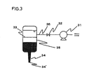
- the discharge device used for the slurry containing solder powder and configured as illustrated in FIG. 2 may be modified to a configuration which, as shown in FIG. 3 , has the suction pipe as for air, the delivery pipe, the first pump and the first switch valve and the second pump and the second switch valve disposed therein consolidated into an assembly consisting of a switching delivery pipe 36 as for air, a pump 31 and a valve 32 plus a filter 33 allowing no passage of the solder powder in the tank.
- the filter is disposed in the lower part of the position at which a switching delivery pipe 36 is attached to the tank.
- the solder powder has no possibility of passing the pump 31 and the valve 32.
- the operation of sucking and discharging the slurry via a discharge and suction port 34' of a discharge and suction pipe 34 is carried out by reversing the motion of the pump 31 and the possibility that the solder powder stored in a tank 35 will flow into the pump 31 and the switch valve 32 and consequently the solder powder will be crushed by the machine parts, such as the pump and the switch valve, is nil.
- the device of this configuration it is made possible to supply the solder powder stable in shape.
- the use of the discharge device described above can materialize a method for forming a solder circuit that does not pass the solder powder through the pump or the switch valve in the discharging device.
- the concentration of the solder powder in the slurry is set preferably in the range of 0.5 volume % to 10 volume % and more preferably in the range of 3 volume % to 8 volume %.
- the slurry containing the solder powder that is used in this invention prefers to use water as its solvent.
- water For the purpose of preventing the solder powder from being oxidized with water, it is favorable to use deoxidized water or add corrosion inhibitor to the water.
- the method of the treatment contemplated by this invention can be effectively used not only for the aforementioned solder precoat circuit board but also for the formation of bumps aimed at joining a BGA (ball grid array) or a CSP (chip size package). These are naturally embraced in the solder circuit board contemplated by this invention.
- the metallic compositions for the solder powder to be used in the method for producing the solder circuit board include Sn-Pb-based, Sn-Pb-Ag-based, Sn-Pb-Bi-based, Sn-Pb-Bi-Ag-based and Sn-Pb-Cd-based compositions, for example.
- the eutectic solder consisting of 63 mass % of Sn and 37 mass % of Pb (hereinafter expressed as 63Sn-37Pb) and playing a central role, 62Sn-36Pb-2Ag, 62.6Sn-37Pb-0.4Ag, 60Sn-40Pb, 50Sn-50Pb, 30Sn-70Pb, 25Sn-75Pb, 10Sn-88Pb-2Ag, 46Sn-8Bi-46Pb, 57Sn-3Bi-40Pb, 42Sn-42Pb-14Bi-2Ag, 45Sn-40Pb-15Bi, 50Sn-32Pb-18Cd, 48Sn-52In, 43Sn-57Bi, 97In-3Ag, 58Sn-42In, 95In-5Bi, 60Sn-40Bi, 91Sn-9Zn, 96.5Sn-3.5Ag, 99.3Sn-0.7Cu, 95Sn-52In, 43Sn-57B
- the particle diameter of the solder powder is selected based on the thickness of the solder coat.
- JIS Japanese Industrial Standards
- the method that uses a standard sieve and a simple balance as specified by JIS can be adopted. The determination may be otherwise accomplished by the image analysis with a microscope or a Coulter counter based on the electrozone method.
- the principle thereof is entered in " Powder Technology Handbook" (compiled by the Society of Powder Technology, Japan, 2nd edition, pp 19-20 ).
- This counter determines the particle diameter distribution of powder by causing a solution having the powder dispersed therein to pass through a fine hole opened in a diaphragm and measuring the change in electric resistance on both sides of the fine hole. It can determine the ratio of pieces of particle diameter with high repeatability.
- the average particle diameter of the solder powder of this invention can be determined by using the method described above.
- the solder circuit board fabricated using the device of this invention can be advantageously used for the method of mounting electronic parts that comprises the steps of mounting electronic parts and joining the electronic parts by reflowing solder.
- the electronic parts can be joined to the parts of the solder circuit board fabricated by the device of this invention that require their adhesion by applying solder paste to the parts as by the printing method, mounting the electronic parts in position, then heating them, thereby fusing the solder powder in the solder paste, and hardening the fused solder powder, for example.
- the surface-mount technology As a means for joining the electronic parts to the solder circuit board, the surface-mount technology (SMT) may be used.
- This mounting method starts from preparing a solder circuit board by this invention or by the method for printing the solder paste.
- the solder paste is applied to the portions of the circuit pattern that require adhesion of electronic parts.
- the electronic parts, such as chip parts and QFP, to which solder has been attached or reflowed by the method of this invention are mounted on the solder paste of the circuit pattern and are collectively soldered thereto by the heat source of reflow.
- the heat sources of reflow an air-heating furnace, an infrared furnace, condensation soldering equipment and light beam soldering equipment may be used.
- the preheating temperature is 130 to 180°C, preferably 130 to 150°C, and the preheating time is 60 to 120 seconds, preferably 60 to 90 seconds.
- the reflow temperature is +20 to +50°C based on the melting point of the alloy to be used, preferably +20 to +30°C based on the melting point of the alloy, and the reflow time is 30 to 60 seconds, preferably 30 to 40 seconds.
- the reflow process can be carried out in nitrogen or in the air.
- nitrogen reflow by keeping the oxygen concentration of 5 volume % or less, preferably 0.5 volume % or less, it is made possible to enhance the wettability of the solder circuit with the solder and reduce the occurrence of solder balls as compared with the air reflow and ensue stable treatment.
- solder circuit board is cooled to complete the surface mounting.
- the method for the production of electronic part joints according to this method of mounting may be carried out on both sides of a printed-wiring board.
- LSI high-density integrated circuits
- resistors capacitors
- transformers inductances
- filters oscillators and transducers
- a printed-wiring board having the minimum electrode interval of 50 ⁇ m and an electrode diameter of 80 ⁇ m was fabricated. Copper was used for a conductive circuit.
- tackifier compound solution As the tackifier compound solution, a 2 mass % aqueous solution of an imidazole-based compound having C 11 H 23 as the alkyl group of R12 and a hydrogen atom as R1 1 in general formula (3) was adjusted to a pH of about 4 with acetic acid prior to use. This aqueous solution was heated to 40°C. In the heated aqueous solution, the printed-wiring board pretreated with an aqueous hydrochloric acid solution was immersed for three minutes to form a tacky substance on the surface of the copper circuit.
- the slurry containing solder powder was produced by mixing about 20 g of solder powder of 96.5Sn-3.5Ag having an average particle diameter of 70 ⁇ m (the average particle diameter of the solder powder determined by the use of a Microtrac®) with about 100 g of deoxidized pure water.
- the device used for discharging the slurry containing the solder powder was configured as illustrated in FIG. 2 .
- the slurry containing the solder powder produced as described above was sucked via the slurry discharge and suction pipe 22 in FIG. 2 into the tank 21 by opening the switch valve 24. Then, the discharge port 22' was set on the substrate to which tackiness had been imparted. This time, the switch valve 26 was opened to discharge the slurry containing the solder powder so as to cover the substrate.
- the powder so rinsed was recovered and used again for the attachment of solder powder.
- the printed-wiring board was placed in an oven at 240°C to fuse the solder powder and form solder bumps of 96.5Sn-3.5Ag in a thickness of about 50 ⁇ m on the copper circuit part. In the soldered circuit, bridges and the like were not formed at all.
- a method for producing an electronic circuit board by imparting tackiness to a metal exposed part on a substrate, thereby inducing adhesion of solder powder to the taky part, and then heating the printed-wiring board, thereby fusing the solder and forming a soldered circuit using a device of this invention a method that enables production of an electronic circuit board of markedly enhanced reliability while effectively reducing the short circuit with the solder metal between the adjacent circuit patterns even in a fine circuit pattern has been perfected.
- a circuit board possessing a fine circuit pattern, manifesting high reliability and having mounted circuit parts allows miniaturization and impartation of high reliability.
Claims (4)
- Vorrichtung zum Abgeben einer Lötpulver enthaltenden Aufschlämmung, die für ein Verfahren zum Bilden einer gelöteten Schaltung auf einer Oberfläche eines Schaltkreises auf einer Leiterplatte eingesetzt wird, welches das Übertragen von Klebrigkeit auf die Oberfläche, das Abgeben der das Lötpulver enthaltenden Aufschlämmung in den erhaltenen klebrigen Bereich, wodurch die Anhaftung des Lötpulvers an diesen zugelassen wird, und dann das Erwärmen der Leiterplatte umfasst, wodurch das Lot verschmolzen wird, und welche einen Behälter (21) zum Lagern der Aufschlämmung, eine in dem Behälter (21) angebrachte Leitung (22) zum Abgeben und Saugen der Aufschlämmung und eine Zuführleitung (28) und eine verbundene erste Pumpe (25) für Gas oder Lösungsmittel umfaßt, das für die Freisetzung der in dem Behälter (21) gelagerten Aufschlämmung über die Leitung (22) zum Abgeben und Saugen der Aufschlämmung eingesetzt werden soll, dadurch gekennzeichnet, dass die Vorrichtung auch eine Saugleitung (27) und eine verbundene zweite Pumpe (23) für Gas oder Lösungsmittel umfaßt, das für das Lagern der Aufschlämmung in dem Behälter (21) über die Leitung (22) zum Abgeben und Saugen der Aufschlämmung eingesetzt wird.
- Vorrichtung zum Abgeben einer Aufschlämmung nach Anspruch 1, wobei die Saugleitung (27) und die Zuführleitung (28) für Gas oder Lösungsmittel mit mindestens einer Pumpe (23, 25) und einem Schaltventil (24, 26) ausgestattet sind.
- Vorrichtung zum Abgeben einer Lötpulver enthaltenden Aufschlämmung, die für ein Verfahren zum Bilden einer gelöteten Schaltung auf einer Oberfläche eines Schaltkreises auf einer Leiterplatte eingesetzt wird, welches das Übertragen von Klebrigkeit auf die Oberfläche, das Abgeben der Lötpulver enthaltenden Aufschlämmung in den erhaltenen klebrigen Bereich, wodurch die Anhaftung des Lötpulvers daran zugelassen wird, und dann das Erwärmen der Leiterplatte umfasst, wodurch das Lot verschmolzen wird, und welche einen Behälter (35) zum Lagern der Aufschlämmung und eine Leitung (34) zum Abgeben und Saugen der Aufschlämmung umfasst, dadurch gekennzeichnet, dass die Vorrichtung ebenfalls eine umschaltbare Zuführleitung (36) und eine verbundene reversible Pumpe (31) für Gas oder Lösungsmittel umfaßt, das für das Saugen der Aufschlämmung über die Leitung (34) zum Abgeben und Saugen der Aufschlämmung zum Lagern der Aufschlämmung in dem Behälter (35) und für die Freisetzung der in dem Behälter (35) gelagerten Aufschlämmung über die Leitung (34) zum Abgeben und Saugen der Aufschlämmung eingesetzt werden soll, wobei die umschaltbare Zuführleitung (36) für Gas oder Lösungsmittel mit einem Filter (33) versehen ist, der keinen Durchgang des Lötpulvers erlaubt, wobei der Filter an dem unteren Teil der Position, an der die umschaltbare Zuführleitung (36) für Gas oder Lösungsmittel mit dem Behälter (35) verbunden ist, angebracht ist.
- Vorrichtung zum Abgeben einer Lötpulver enthaltenden Aufschlämmung nach Anspruch 3, wobei die um schaltbare Zuführleitung (36) für Gas oder Lösungsmittel mit mindestens einer Pumpe (31), die Gas oder Lösungsmittel saugen oder zuführen kann, und einem Schaltventil (32) versehen ist.
Priority Applications (1)
| Application Number | Priority Date | Filing Date | Title |
|---|---|---|---|
| EP10006438A EP2237651B1 (de) | 2006-10-17 | 2007-10-12 | Verfahren zur Bildung einer Lotschicht auf einer Leiterplatte und Schlammentladungsvorrichtung |
Applications Claiming Priority (2)
| Application Number | Priority Date | Filing Date | Title |
|---|---|---|---|
| JP2006282328 | 2006-10-17 | ||
| PCT/JP2007/070395 WO2008047888A1 (en) | 2006-10-17 | 2007-10-12 | Method for forming solder layer on printed-wiring board and slurry discharge device |
Related Child Applications (1)
| Application Number | Title | Priority Date | Filing Date |
|---|---|---|---|
| EP10006438.5 Division-Into | 2010-06-21 |
Publications (3)
| Publication Number | Publication Date |
|---|---|
| EP2082630A1 EP2082630A1 (de) | 2009-07-29 |
| EP2082630A4 EP2082630A4 (de) | 2009-12-30 |
| EP2082630B1 true EP2082630B1 (de) | 2012-01-25 |
Family
ID=39314101
Family Applications (2)
| Application Number | Title | Priority Date | Filing Date |
|---|---|---|---|
| EP10006438A Not-in-force EP2237651B1 (de) | 2006-10-17 | 2007-10-12 | Verfahren zur Bildung einer Lotschicht auf einer Leiterplatte und Schlammentladungsvorrichtung |
| EP07830129A Not-in-force EP2082630B1 (de) | 2006-10-17 | 2007-10-12 | Schlämmenabgabeeinrichtung |
Family Applications Before (1)
| Application Number | Title | Priority Date | Filing Date |
|---|---|---|---|
| EP10006438A Not-in-force EP2237651B1 (de) | 2006-10-17 | 2007-10-12 | Verfahren zur Bildung einer Lotschicht auf einer Leiterplatte und Schlammentladungsvorrichtung |
Country Status (8)
| Country | Link |
|---|---|
| US (1) | US20100009070A1 (de) |
| EP (2) | EP2237651B1 (de) |
| JP (1) | JP5001113B2 (de) |
| KR (1) | KR101108960B1 (de) |
| CN (1) | CN101536620B (de) |
| AT (2) | ATE543374T1 (de) |
| TW (1) | TWI411363B (de) |
| WO (1) | WO2008047888A1 (de) |
Families Citing this family (8)
| Publication number | Priority date | Publication date | Assignee | Title |
|---|---|---|---|---|
| JP4576270B2 (ja) * | 2005-03-29 | 2010-11-04 | 昭和電工株式会社 | ハンダ回路基板の製造方法 |
| WO2007029866A1 (en) * | 2005-09-09 | 2007-03-15 | Showa Denko K.K. | Method for attachment of solder powder to electronic circuit board and soldered electronic circuit board |
| JP4920401B2 (ja) * | 2006-12-27 | 2012-04-18 | 昭和電工株式会社 | 導電性回路基板の製造方法 |
| KR102223165B1 (ko) * | 2013-03-14 | 2021-03-03 | 무사시 엔지니어링 가부시키가이샤 | 액체 재료 토출 장치, 그 도포 장치 및 도포 방법 |
| CN106425004A (zh) * | 2016-10-18 | 2017-02-22 | 成都言行果科技有限公司 | 电子设备熔接装置的多点位焊料送料装置 |
| CN106363267A (zh) * | 2016-10-18 | 2017-02-01 | 成都言行果科技有限公司 | 电子设备熔接装置的过滤型焊料送料装置 |
| US11766729B2 (en) * | 2017-09-28 | 2023-09-26 | International Business Machines Corporation | Molten solder injection head with vacuum filter and differential gauge system |
| CN110557897A (zh) * | 2019-10-09 | 2019-12-10 | 新野县立新电子有限公司 | 一种环保印刷线路板生产工艺 |
Family Cites Families (25)
| Publication number | Priority date | Publication date | Assignee | Title |
|---|---|---|---|---|
| EP0187746A1 (de) * | 1984-07-18 | 1986-07-23 | AT&T Corp. | Verfahren und apparat zum vielpunktverteilen von zähflüssigem material |
| US4572103A (en) * | 1984-12-20 | 1986-02-25 | Engel Harold J | Solder paste dispenser for SMD circuit boards |
| JPS61155075U (de) * | 1985-03-12 | 1986-09-26 | ||
| JPH03152A (ja) * | 1989-05-24 | 1991-01-07 | Sanyo Electric Co Ltd | 塗布装置 |
| KR940009257B1 (ko) * | 1990-07-10 | 1994-10-06 | 무사시엔지니어링 가부시기가이샤 | 액체 정량 토출장치 |
| JP3000152B2 (ja) * | 1990-08-31 | 2000-01-17 | 名古屋工業大学長 | 高圧ガス噴射装置 |
| JP2592757B2 (ja) | 1992-10-30 | 1997-03-19 | 昭和電工株式会社 | はんだ回路基板及びその形成方法 |
| US6476487B2 (en) * | 1992-10-30 | 2002-11-05 | Showa Denko K.K. | Solder circuit |
| US5346118A (en) * | 1993-09-28 | 1994-09-13 | At&T Bell Laboratories | Surface mount solder assembly of leadless integrated circuit packages to substrates |
| JPH11163501A (ja) * | 1997-12-02 | 1999-06-18 | Rohm Co Ltd | 電子部品の実装方法、およびその方法によって製造された電子回路装置 |
| JP2000062138A (ja) | 1998-08-19 | 2000-02-29 | Matsushita Electric Ind Co Ltd | 印刷装置 |
| US6386433B1 (en) * | 1999-08-24 | 2002-05-14 | Kulicke & Soffa Investments, Inc. | Solder ball delivery and reflow apparatus and method |
| US6564105B2 (en) * | 2000-01-21 | 2003-05-13 | Medtronic Minimed, Inc. | Method and apparatus for communicating between an ambulatory medical device and a control device via telemetry using randomized data |
| SE518642C2 (sv) * | 2000-07-11 | 2002-11-05 | Mydata Automation Ab | Förfarande, anordning för att förse ett substrat med visköst medium, anordning för korrigering av applikationsfel samt användningen av utskjutnings- organ för korrigering av appliceringsfel |
| JP2003000152A (ja) * | 2001-06-25 | 2003-01-07 | Mitsubishi Heavy Ind Ltd | ソフトクリームフリーザ |
| JP2004221378A (ja) * | 2003-01-16 | 2004-08-05 | Matsushita Electric Ind Co Ltd | 電子部品の実装方法 |
| EP1624521B1 (de) * | 2003-03-31 | 2013-04-24 | Tokyo Gas Company Limited | Verfahren zur herstellung eines festoxid-brennstoffzellenmoduls |
| TWI259626B (en) * | 2004-06-11 | 2006-08-01 | Hon Hai Prec Ind Co Ltd | Electrical card connector |
| US7381371B2 (en) * | 2004-01-16 | 2008-06-03 | Heathrow Scientific Llc | Pipette device with pivotable nozzle assembly |
| JP2006064545A (ja) * | 2004-08-27 | 2006-03-09 | Mitsubishi Chemicals Corp | 流体吐出機構及び流体吐出方法並びに流体分注装置 |
| JP4688475B2 (ja) * | 2004-11-15 | 2011-05-25 | 株式会社タムラ製作所 | はんだ材料供給装置及びこれを用いたはんだ材料供給方法 |
| JP4576270B2 (ja) * | 2005-03-29 | 2010-11-04 | 昭和電工株式会社 | ハンダ回路基板の製造方法 |
| JP4670436B2 (ja) | 2005-03-31 | 2011-04-13 | 株式会社豊田自動織機 | 産業車両のヘッドガード |
| TWM275090U (en) * | 2005-04-22 | 2005-09-11 | Neng-Kuei Ye | Low speed material supply device for mixing materials |
| WO2007029866A1 (en) * | 2005-09-09 | 2007-03-15 | Showa Denko K.K. | Method for attachment of solder powder to electronic circuit board and soldered electronic circuit board |
-
2007
- 2007-10-12 EP EP10006438A patent/EP2237651B1/de not_active Not-in-force
- 2007-10-12 CN CN2007800426322A patent/CN101536620B/zh not_active Expired - Fee Related
- 2007-10-12 AT AT07830129T patent/ATE543374T1/de active
- 2007-10-12 US US12/445,379 patent/US20100009070A1/en not_active Abandoned
- 2007-10-12 AT AT10006438T patent/ATE536735T1/de active
- 2007-10-12 KR KR1020097008376A patent/KR101108960B1/ko not_active IP Right Cessation
- 2007-10-12 WO PCT/JP2007/070395 patent/WO2008047888A1/en active Application Filing
- 2007-10-12 EP EP07830129A patent/EP2082630B1/de not_active Not-in-force
- 2007-10-16 JP JP2007268752A patent/JP5001113B2/ja not_active Expired - Fee Related
- 2007-10-17 TW TW096138910A patent/TWI411363B/zh not_active IP Right Cessation
Also Published As
| Publication number | Publication date |
|---|---|
| US20100009070A1 (en) | 2010-01-14 |
| EP2237651B1 (de) | 2011-12-07 |
| TW200838374A (en) | 2008-09-16 |
| CN101536620B (zh) | 2011-04-06 |
| TWI411363B (zh) | 2013-10-01 |
| JP2008124447A (ja) | 2008-05-29 |
| EP2082630A1 (de) | 2009-07-29 |
| JP5001113B2 (ja) | 2012-08-15 |
| WO2008047888A1 (en) | 2008-04-24 |
| EP2237651A1 (de) | 2010-10-06 |
| ATE536735T1 (de) | 2011-12-15 |
| CN101536620A (zh) | 2009-09-16 |
| KR101108960B1 (ko) | 2012-01-31 |
| KR20090079902A (ko) | 2009-07-22 |
| ATE543374T1 (de) | 2012-02-15 |
| EP2082630A4 (de) | 2009-12-30 |
Similar Documents
| Publication | Publication Date | Title |
|---|---|---|
| EP2082630B1 (de) | Schlämmenabgabeeinrichtung | |
| EP1864559B1 (de) | Herstellungsverfahren für eine lot-leiterplatte | |
| EP1745684B1 (de) | Verfahren zur herstellung einer elektronischen leiterplatte | |
| US20100038411A1 (en) | Method of producing conductive circuit board | |
| WO2008016128A1 (en) | Production method of soldier circuit board | |
| KR101047869B1 (ko) | 도전성 회로 기판의 제조 방법 | |
| WO2007029866A1 (en) | Method for attachment of solder powder to electronic circuit board and soldered electronic circuit board | |
| WO2007007865A1 (en) | Method for attachment of solder powder to electronic circuit board and solder-attached electronic circuit board | |
| JP4819611B2 (ja) | ハンダ回路基板の製造方法 | |
| JP2008041867A (ja) | ハンダ回路基板の製造方法 |
Legal Events
| Date | Code | Title | Description |
|---|---|---|---|
| PUAI | Public reference made under article 153(3) epc to a published international application that has entered the european phase |
Free format text: ORIGINAL CODE: 0009012 |
|
| 17P | Request for examination filed |
Effective date: 20090513 |
|
| AK | Designated contracting states |
Kind code of ref document: A1 Designated state(s): AT BE BG CH CY CZ DE DK EE ES FI FR GB GR HU IE IS IT LI LT LU LV MC MT NL PL PT RO SE SI SK TR |
|
| A4 | Supplementary search report drawn up and despatched |
Effective date: 20091130 |
|
| DAX | Request for extension of the european patent (deleted) | ||
| 17Q | First examination report despatched |
Effective date: 20100218 |
|
| GRAP | Despatch of communication of intention to grant a patent |
Free format text: ORIGINAL CODE: EPIDOSNIGR1 |
|
| RIC1 | Information provided on ipc code assigned before grant |
Ipc: H05K 3/24 20060101ALI20110114BHEP Ipc: H05K 3/34 20060101AFI20110114BHEP |
|
| RTI1 | Title (correction) |
Free format text: SLURRY DISCHARGE DEVICE |
|
| RIC1 | Information provided on ipc code assigned before grant |
Ipc: B23K 3/06 20060101ALI20110121BHEP Ipc: H05K 3/34 20060101AFI20110121BHEP |
|
| GRAS | Grant fee paid |
Free format text: ORIGINAL CODE: EPIDOSNIGR3 |
|
| GRAA | (expected) grant |
Free format text: ORIGINAL CODE: 0009210 |
|
| AK | Designated contracting states |
Kind code of ref document: B1 Designated state(s): AT BE BG CH CY CZ DE DK EE ES FI FR GB GR HU IE IS IT LI LT LU LV MC MT NL PL PT RO SE SI SK TR |
|
| REG | Reference to a national code |
Ref country code: GB Ref legal event code: FG4D |
|
| REG | Reference to a national code |
Ref country code: CH Ref legal event code: EP |
|
| REG | Reference to a national code |
Ref country code: AT Ref legal event code: REF Ref document number: 543374 Country of ref document: AT Kind code of ref document: T Effective date: 20120215 |
|
| REG | Reference to a national code |
Ref country code: IE Ref legal event code: FG4D |
|
| REG | Reference to a national code |
Ref country code: DE Ref legal event code: R096 Ref document number: 602007020329 Country of ref document: DE Effective date: 20120322 |
|
| REG | Reference to a national code |
Ref country code: NL Ref legal event code: VDEP Effective date: 20120125 |
|
| LTIE | Lt: invalidation of european patent or patent extension |
Effective date: 20120125 |
|
| PG25 | Lapsed in a contracting state [announced via postgrant information from national office to epo] |
Ref country code: LT Free format text: LAPSE BECAUSE OF FAILURE TO SUBMIT A TRANSLATION OF THE DESCRIPTION OR TO PAY THE FEE WITHIN THE PRESCRIBED TIME-LIMIT Effective date: 20120125 Ref country code: NL Free format text: LAPSE BECAUSE OF FAILURE TO SUBMIT A TRANSLATION OF THE DESCRIPTION OR TO PAY THE FEE WITHIN THE PRESCRIBED TIME-LIMIT Effective date: 20120125 Ref country code: BE Free format text: LAPSE BECAUSE OF FAILURE TO SUBMIT A TRANSLATION OF THE DESCRIPTION OR TO PAY THE FEE WITHIN THE PRESCRIBED TIME-LIMIT Effective date: 20120125 Ref country code: BG Free format text: LAPSE BECAUSE OF FAILURE TO SUBMIT A TRANSLATION OF THE DESCRIPTION OR TO PAY THE FEE WITHIN THE PRESCRIBED TIME-LIMIT Effective date: 20120425 Ref country code: IS Free format text: LAPSE BECAUSE OF FAILURE TO SUBMIT A TRANSLATION OF THE DESCRIPTION OR TO PAY THE FEE WITHIN THE PRESCRIBED TIME-LIMIT Effective date: 20120525 |
|
| PG25 | Lapsed in a contracting state [announced via postgrant information from national office to epo] |
Ref country code: PT Free format text: LAPSE BECAUSE OF FAILURE TO SUBMIT A TRANSLATION OF THE DESCRIPTION OR TO PAY THE FEE WITHIN THE PRESCRIBED TIME-LIMIT Effective date: 20120525 Ref country code: LV Free format text: LAPSE BECAUSE OF FAILURE TO SUBMIT A TRANSLATION OF THE DESCRIPTION OR TO PAY THE FEE WITHIN THE PRESCRIBED TIME-LIMIT Effective date: 20120125 Ref country code: GR Free format text: LAPSE BECAUSE OF FAILURE TO SUBMIT A TRANSLATION OF THE DESCRIPTION OR TO PAY THE FEE WITHIN THE PRESCRIBED TIME-LIMIT Effective date: 20120426 Ref country code: PL Free format text: LAPSE BECAUSE OF FAILURE TO SUBMIT A TRANSLATION OF THE DESCRIPTION OR TO PAY THE FEE WITHIN THE PRESCRIBED TIME-LIMIT Effective date: 20120125 Ref country code: FI Free format text: LAPSE BECAUSE OF FAILURE TO SUBMIT A TRANSLATION OF THE DESCRIPTION OR TO PAY THE FEE WITHIN THE PRESCRIBED TIME-LIMIT Effective date: 20120125 |
|
| REG | Reference to a national code |
Ref country code: AT Ref legal event code: MK05 Ref document number: 543374 Country of ref document: AT Kind code of ref document: T Effective date: 20120125 |
|
| PG25 | Lapsed in a contracting state [announced via postgrant information from national office to epo] |
Ref country code: CY Free format text: LAPSE BECAUSE OF FAILURE TO SUBMIT A TRANSLATION OF THE DESCRIPTION OR TO PAY THE FEE WITHIN THE PRESCRIBED TIME-LIMIT Effective date: 20120125 |
|
| PG25 | Lapsed in a contracting state [announced via postgrant information from national office to epo] |
Ref country code: EE Free format text: LAPSE BECAUSE OF FAILURE TO SUBMIT A TRANSLATION OF THE DESCRIPTION OR TO PAY THE FEE WITHIN THE PRESCRIBED TIME-LIMIT Effective date: 20120125 Ref country code: SE Free format text: LAPSE BECAUSE OF FAILURE TO SUBMIT A TRANSLATION OF THE DESCRIPTION OR TO PAY THE FEE WITHIN THE PRESCRIBED TIME-LIMIT Effective date: 20120125 Ref country code: SI Free format text: LAPSE BECAUSE OF FAILURE TO SUBMIT A TRANSLATION OF THE DESCRIPTION OR TO PAY THE FEE WITHIN THE PRESCRIBED TIME-LIMIT Effective date: 20120125 Ref country code: DK Free format text: LAPSE BECAUSE OF FAILURE TO SUBMIT A TRANSLATION OF THE DESCRIPTION OR TO PAY THE FEE WITHIN THE PRESCRIBED TIME-LIMIT Effective date: 20120125 Ref country code: CZ Free format text: LAPSE BECAUSE OF FAILURE TO SUBMIT A TRANSLATION OF THE DESCRIPTION OR TO PAY THE FEE WITHIN THE PRESCRIBED TIME-LIMIT Effective date: 20120125 Ref country code: RO Free format text: LAPSE BECAUSE OF FAILURE TO SUBMIT A TRANSLATION OF THE DESCRIPTION OR TO PAY THE FEE WITHIN THE PRESCRIBED TIME-LIMIT Effective date: 20120125 |
|
| PG25 | Lapsed in a contracting state [announced via postgrant information from national office to epo] |
Ref country code: SK Free format text: LAPSE BECAUSE OF FAILURE TO SUBMIT A TRANSLATION OF THE DESCRIPTION OR TO PAY THE FEE WITHIN THE PRESCRIBED TIME-LIMIT Effective date: 20120125 Ref country code: IT Free format text: LAPSE BECAUSE OF FAILURE TO SUBMIT A TRANSLATION OF THE DESCRIPTION OR TO PAY THE FEE WITHIN THE PRESCRIBED TIME-LIMIT Effective date: 20120125 |
|
| PLBE | No opposition filed within time limit |
Free format text: ORIGINAL CODE: 0009261 |
|
| STAA | Information on the status of an ep patent application or granted ep patent |
Free format text: STATUS: NO OPPOSITION FILED WITHIN TIME LIMIT |
|
| 26N | No opposition filed |
Effective date: 20121026 |
|
| PG25 | Lapsed in a contracting state [announced via postgrant information from national office to epo] |
Ref country code: AT Free format text: LAPSE BECAUSE OF FAILURE TO SUBMIT A TRANSLATION OF THE DESCRIPTION OR TO PAY THE FEE WITHIN THE PRESCRIBED TIME-LIMIT Effective date: 20120125 |
|
| REG | Reference to a national code |
Ref country code: DE Ref legal event code: R097 Ref document number: 602007020329 Country of ref document: DE Effective date: 20121026 |
|
| PG25 | Lapsed in a contracting state [announced via postgrant information from national office to epo] |
Ref country code: ES Free format text: LAPSE BECAUSE OF FAILURE TO SUBMIT A TRANSLATION OF THE DESCRIPTION OR TO PAY THE FEE WITHIN THE PRESCRIBED TIME-LIMIT Effective date: 20120506 |
|
| PG25 | Lapsed in a contracting state [announced via postgrant information from national office to epo] |
Ref country code: MC Free format text: LAPSE BECAUSE OF NON-PAYMENT OF DUE FEES Effective date: 20121031 |
|
| REG | Reference to a national code |
Ref country code: CH Ref legal event code: PL |
|
| GBPC | Gb: european patent ceased through non-payment of renewal fee |
Effective date: 20121012 |
|
| REG | Reference to a national code |
Ref country code: IE Ref legal event code: MM4A |
|
| REG | Reference to a national code |
Ref country code: FR Ref legal event code: ST Effective date: 20130628 |
|
| PG25 | Lapsed in a contracting state [announced via postgrant information from national office to epo] |
Ref country code: IE Free format text: LAPSE BECAUSE OF NON-PAYMENT OF DUE FEES Effective date: 20121012 Ref country code: LI Free format text: LAPSE BECAUSE OF NON-PAYMENT OF DUE FEES Effective date: 20121031 Ref country code: CH Free format text: LAPSE BECAUSE OF NON-PAYMENT OF DUE FEES Effective date: 20121031 Ref country code: GB Free format text: LAPSE BECAUSE OF NON-PAYMENT OF DUE FEES Effective date: 20121012 |
|
| PG25 | Lapsed in a contracting state [announced via postgrant information from national office to epo] |
Ref country code: FR Free format text: LAPSE BECAUSE OF NON-PAYMENT OF DUE FEES Effective date: 20121031 |
|
| PG25 | Lapsed in a contracting state [announced via postgrant information from national office to epo] |
Ref country code: MT Free format text: LAPSE BECAUSE OF FAILURE TO SUBMIT A TRANSLATION OF THE DESCRIPTION OR TO PAY THE FEE WITHIN THE PRESCRIBED TIME-LIMIT Effective date: 20120125 |
|
| PG25 | Lapsed in a contracting state [announced via postgrant information from national office to epo] |
Ref country code: TR Free format text: LAPSE BECAUSE OF FAILURE TO SUBMIT A TRANSLATION OF THE DESCRIPTION OR TO PAY THE FEE WITHIN THE PRESCRIBED TIME-LIMIT Effective date: 20120125 |
|
| PG25 | Lapsed in a contracting state [announced via postgrant information from national office to epo] |
Ref country code: LU Free format text: LAPSE BECAUSE OF NON-PAYMENT OF DUE FEES Effective date: 20121012 |
|
| PG25 | Lapsed in a contracting state [announced via postgrant information from national office to epo] |
Ref country code: HU Free format text: LAPSE BECAUSE OF FAILURE TO SUBMIT A TRANSLATION OF THE DESCRIPTION OR TO PAY THE FEE WITHIN THE PRESCRIBED TIME-LIMIT Effective date: 20071012 |
|
| PGFP | Annual fee paid to national office [announced via postgrant information from national office to epo] |
Ref country code: DE Payment date: 20171004 Year of fee payment: 11 |
|
| REG | Reference to a national code |
Ref country code: DE Ref legal event code: R119 Ref document number: 602007020329 Country of ref document: DE |
|
| PG25 | Lapsed in a contracting state [announced via postgrant information from national office to epo] |
Ref country code: DE Free format text: LAPSE BECAUSE OF NON-PAYMENT OF DUE FEES Effective date: 20190501 |