EP2073262B1 - Composant semi-conducteur - Google Patents
Composant semi-conducteur Download PDFInfo
- Publication number
- EP2073262B1 EP2073262B1 EP07024487.6A EP07024487A EP2073262B1 EP 2073262 B1 EP2073262 B1 EP 2073262B1 EP 07024487 A EP07024487 A EP 07024487A EP 2073262 B1 EP2073262 B1 EP 2073262B1
- Authority
- EP
- European Patent Office
- Prior art keywords
- semiconductor chip
- contact
- analysis
- semiconductor
- encapsulating material
- Prior art date
- Legal status (The legal status is an assumption and is not a legal conclusion. Google has not performed a legal analysis and makes no representation as to the accuracy of the status listed.)
- Ceased
Links
- 239000004065 semiconductor Substances 0.000 title claims description 112
- 238000012360 testing method Methods 0.000 claims description 18
- 239000000463 material Substances 0.000 claims description 12
- 238000005538 encapsulation Methods 0.000 description 32
- 239000008393 encapsulating agent Substances 0.000 description 25
- 150000001875 compounds Chemical class 0.000 description 18
- 229940126214 compound 3 Drugs 0.000 description 15
- 230000007547 defect Effects 0.000 description 6
- 239000010410 layer Substances 0.000 description 5
- 230000007613 environmental effect Effects 0.000 description 3
- 238000004519 manufacturing process Methods 0.000 description 3
- 238000004382 potting Methods 0.000 description 3
- 239000002344 surface layer Substances 0.000 description 2
- 239000012790 adhesive layer Substances 0.000 description 1
- 239000004020 conductor Substances 0.000 description 1
- 230000002950 deficient Effects 0.000 description 1
- 239000003822 epoxy resin Substances 0.000 description 1
- 238000010304 firing Methods 0.000 description 1
- 238000000227 grinding Methods 0.000 description 1
- 238000005259 measurement Methods 0.000 description 1
- 238000003801 milling Methods 0.000 description 1
- 239000004033 plastic Substances 0.000 description 1
- 229920000647 polyepoxide Polymers 0.000 description 1
- 238000000275 quality assurance Methods 0.000 description 1
- 230000000717 retained effect Effects 0.000 description 1
- 238000010079 rubber tapping Methods 0.000 description 1
- 239000000126 substance Substances 0.000 description 1
- 239000006228 supernatant Substances 0.000 description 1
- 238000003631 wet chemical etching Methods 0.000 description 1
Images


Classifications
-
- H—ELECTRICITY
- H01—ELECTRIC ELEMENTS
- H01L—SEMICONDUCTOR DEVICES NOT COVERED BY CLASS H10
- H01L23/00—Details of semiconductor or other solid state devices
- H01L23/28—Encapsulations, e.g. encapsulating layers, coatings, e.g. for protection
- H01L23/31—Encapsulations, e.g. encapsulating layers, coatings, e.g. for protection characterised by the arrangement or shape
- H01L23/3107—Encapsulations, e.g. encapsulating layers, coatings, e.g. for protection characterised by the arrangement or shape the device being completely enclosed
-
- H—ELECTRICITY
- H01—ELECTRIC ELEMENTS
- H01L—SEMICONDUCTOR DEVICES NOT COVERED BY CLASS H10
- H01L22/00—Testing or measuring during manufacture or treatment; Reliability measurements, i.e. testing of parts without further processing to modify the parts as such; Structural arrangements therefor
- H01L22/30—Structural arrangements specially adapted for testing or measuring during manufacture or treatment, or specially adapted for reliability measurements
- H01L22/34—Circuits for electrically characterising or monitoring manufacturing processes, e. g. whole test die, wafers filled with test structures, on-board-devices incorporated on each die, process control monitors or pad structures thereof, devices in scribe line
-
- H—ELECTRICITY
- H01—ELECTRIC ELEMENTS
- H01L—SEMICONDUCTOR DEVICES NOT COVERED BY CLASS H10
- H01L24/00—Arrangements for connecting or disconnecting semiconductor or solid-state bodies; Methods or apparatus related thereto
- H01L24/01—Means for bonding being attached to, or being formed on, the surface to be connected, e.g. chip-to-package, die-attach, "first-level" interconnects; Manufacturing methods related thereto
- H01L24/02—Bonding areas ; Manufacturing methods related thereto
- H01L24/04—Structure, shape, material or disposition of the bonding areas prior to the connecting process
- H01L24/05—Structure, shape, material or disposition of the bonding areas prior to the connecting process of an individual bonding area
-
- H—ELECTRICITY
- H01—ELECTRIC ELEMENTS
- H01L—SEMICONDUCTOR DEVICES NOT COVERED BY CLASS H10
- H01L24/00—Arrangements for connecting or disconnecting semiconductor or solid-state bodies; Methods or apparatus related thereto
- H01L24/01—Means for bonding being attached to, or being formed on, the surface to be connected, e.g. chip-to-package, die-attach, "first-level" interconnects; Manufacturing methods related thereto
- H01L24/02—Bonding areas ; Manufacturing methods related thereto
- H01L24/04—Structure, shape, material or disposition of the bonding areas prior to the connecting process
- H01L24/06—Structure, shape, material or disposition of the bonding areas prior to the connecting process of a plurality of bonding areas
-
- H—ELECTRICITY
- H01—ELECTRIC ELEMENTS
- H01L—SEMICONDUCTOR DEVICES NOT COVERED BY CLASS H10
- H01L24/00—Arrangements for connecting or disconnecting semiconductor or solid-state bodies; Methods or apparatus related thereto
- H01L24/01—Means for bonding being attached to, or being formed on, the surface to be connected, e.g. chip-to-package, die-attach, "first-level" interconnects; Manufacturing methods related thereto
- H01L24/42—Wire connectors; Manufacturing methods related thereto
- H01L24/47—Structure, shape, material or disposition of the wire connectors after the connecting process
- H01L24/48—Structure, shape, material or disposition of the wire connectors after the connecting process of an individual wire connector
-
- H—ELECTRICITY
- H01—ELECTRIC ELEMENTS
- H01L—SEMICONDUCTOR DEVICES NOT COVERED BY CLASS H10
- H01L24/00—Arrangements for connecting or disconnecting semiconductor or solid-state bodies; Methods or apparatus related thereto
- H01L24/01—Means for bonding being attached to, or being formed on, the surface to be connected, e.g. chip-to-package, die-attach, "first-level" interconnects; Manufacturing methods related thereto
- H01L24/42—Wire connectors; Manufacturing methods related thereto
- H01L24/47—Structure, shape, material or disposition of the wire connectors after the connecting process
- H01L24/49—Structure, shape, material or disposition of the wire connectors after the connecting process of a plurality of wire connectors
-
- H—ELECTRICITY
- H01—ELECTRIC ELEMENTS
- H01L—SEMICONDUCTOR DEVICES NOT COVERED BY CLASS H10
- H01L24/00—Arrangements for connecting or disconnecting semiconductor or solid-state bodies; Methods or apparatus related thereto
- H01L24/73—Means for bonding being of different types provided for in two or more of groups H01L24/10, H01L24/18, H01L24/26, H01L24/34, H01L24/42, H01L24/50, H01L24/63, H01L24/71
-
- H—ELECTRICITY
- H01—ELECTRIC ELEMENTS
- H01L—SEMICONDUCTOR DEVICES NOT COVERED BY CLASS H10
- H01L24/00—Arrangements for connecting or disconnecting semiconductor or solid-state bodies; Methods or apparatus related thereto
- H01L24/91—Methods for connecting semiconductor or solid state bodies including different methods provided for in two or more of groups H01L24/80 - H01L24/90
-
- H—ELECTRICITY
- H01—ELECTRIC ELEMENTS
- H01L—SEMICONDUCTOR DEVICES NOT COVERED BY CLASS H10
- H01L2224/00—Indexing scheme for arrangements for connecting or disconnecting semiconductor or solid-state bodies and methods related thereto as covered by H01L24/00
- H01L2224/01—Means for bonding being attached to, or being formed on, the surface to be connected, e.g. chip-to-package, die-attach, "first-level" interconnects; Manufacturing methods related thereto
- H01L2224/02—Bonding areas; Manufacturing methods related thereto
- H01L2224/04—Structure, shape, material or disposition of the bonding areas prior to the connecting process
- H01L2224/0401—Bonding areas specifically adapted for bump connectors, e.g. under bump metallisation [UBM]
-
- H—ELECTRICITY
- H01—ELECTRIC ELEMENTS
- H01L—SEMICONDUCTOR DEVICES NOT COVERED BY CLASS H10
- H01L2224/00—Indexing scheme for arrangements for connecting or disconnecting semiconductor or solid-state bodies and methods related thereto as covered by H01L24/00
- H01L2224/01—Means for bonding being attached to, or being formed on, the surface to be connected, e.g. chip-to-package, die-attach, "first-level" interconnects; Manufacturing methods related thereto
- H01L2224/02—Bonding areas; Manufacturing methods related thereto
- H01L2224/04—Structure, shape, material or disposition of the bonding areas prior to the connecting process
- H01L2224/04042—Bonding areas specifically adapted for wire connectors, e.g. wirebond pads
-
- H—ELECTRICITY
- H01—ELECTRIC ELEMENTS
- H01L—SEMICONDUCTOR DEVICES NOT COVERED BY CLASS H10
- H01L2224/00—Indexing scheme for arrangements for connecting or disconnecting semiconductor or solid-state bodies and methods related thereto as covered by H01L24/00
- H01L2224/01—Means for bonding being attached to, or being formed on, the surface to be connected, e.g. chip-to-package, die-attach, "first-level" interconnects; Manufacturing methods related thereto
- H01L2224/02—Bonding areas; Manufacturing methods related thereto
- H01L2224/04—Structure, shape, material or disposition of the bonding areas prior to the connecting process
- H01L2224/05—Structure, shape, material or disposition of the bonding areas prior to the connecting process of an individual bonding area
- H01L2224/0554—External layer
- H01L2224/0555—Shape
- H01L2224/05552—Shape in top view
- H01L2224/05553—Shape in top view being rectangular
-
- H—ELECTRICITY
- H01—ELECTRIC ELEMENTS
- H01L—SEMICONDUCTOR DEVICES NOT COVERED BY CLASS H10
- H01L2224/00—Indexing scheme for arrangements for connecting or disconnecting semiconductor or solid-state bodies and methods related thereto as covered by H01L24/00
- H01L2224/01—Means for bonding being attached to, or being formed on, the surface to be connected, e.g. chip-to-package, die-attach, "first-level" interconnects; Manufacturing methods related thereto
- H01L2224/02—Bonding areas; Manufacturing methods related thereto
- H01L2224/04—Structure, shape, material or disposition of the bonding areas prior to the connecting process
- H01L2224/05—Structure, shape, material or disposition of the bonding areas prior to the connecting process of an individual bonding area
- H01L2224/0554—External layer
- H01L2224/0555—Shape
- H01L2224/05552—Shape in top view
- H01L2224/05554—Shape in top view being square
-
- H—ELECTRICITY
- H01—ELECTRIC ELEMENTS
- H01L—SEMICONDUCTOR DEVICES NOT COVERED BY CLASS H10
- H01L2224/00—Indexing scheme for arrangements for connecting or disconnecting semiconductor or solid-state bodies and methods related thereto as covered by H01L24/00
- H01L2224/01—Means for bonding being attached to, or being formed on, the surface to be connected, e.g. chip-to-package, die-attach, "first-level" interconnects; Manufacturing methods related thereto
- H01L2224/02—Bonding areas; Manufacturing methods related thereto
- H01L2224/04—Structure, shape, material or disposition of the bonding areas prior to the connecting process
- H01L2224/05—Structure, shape, material or disposition of the bonding areas prior to the connecting process of an individual bonding area
- H01L2224/0554—External layer
- H01L2224/0555—Shape
- H01L2224/05556—Shape in side view
-
- H—ELECTRICITY
- H01—ELECTRIC ELEMENTS
- H01L—SEMICONDUCTOR DEVICES NOT COVERED BY CLASS H10
- H01L2224/00—Indexing scheme for arrangements for connecting or disconnecting semiconductor or solid-state bodies and methods related thereto as covered by H01L24/00
- H01L2224/01—Means for bonding being attached to, or being formed on, the surface to be connected, e.g. chip-to-package, die-attach, "first-level" interconnects; Manufacturing methods related thereto
- H01L2224/02—Bonding areas; Manufacturing methods related thereto
- H01L2224/04—Structure, shape, material or disposition of the bonding areas prior to the connecting process
- H01L2224/05—Structure, shape, material or disposition of the bonding areas prior to the connecting process of an individual bonding area
- H01L2224/0554—External layer
- H01L2224/05599—Material
-
- H—ELECTRICITY
- H01—ELECTRIC ELEMENTS
- H01L—SEMICONDUCTOR DEVICES NOT COVERED BY CLASS H10
- H01L2224/00—Indexing scheme for arrangements for connecting or disconnecting semiconductor or solid-state bodies and methods related thereto as covered by H01L24/00
- H01L2224/01—Means for bonding being attached to, or being formed on, the surface to be connected, e.g. chip-to-package, die-attach, "first-level" interconnects; Manufacturing methods related thereto
- H01L2224/10—Bump connectors; Manufacturing methods related thereto
- H01L2224/15—Structure, shape, material or disposition of the bump connectors after the connecting process
- H01L2224/16—Structure, shape, material or disposition of the bump connectors after the connecting process of an individual bump connector
- H01L2224/161—Disposition
- H01L2224/16135—Disposition the bump connector connecting between different semiconductor or solid-state bodies, i.e. chip-to-chip
- H01L2224/16145—Disposition the bump connector connecting between different semiconductor or solid-state bodies, i.e. chip-to-chip the bodies being stacked
-
- H—ELECTRICITY
- H01—ELECTRIC ELEMENTS
- H01L—SEMICONDUCTOR DEVICES NOT COVERED BY CLASS H10
- H01L2224/00—Indexing scheme for arrangements for connecting or disconnecting semiconductor or solid-state bodies and methods related thereto as covered by H01L24/00
- H01L2224/01—Means for bonding being attached to, or being formed on, the surface to be connected, e.g. chip-to-package, die-attach, "first-level" interconnects; Manufacturing methods related thereto
- H01L2224/26—Layer connectors, e.g. plate connectors, solder or adhesive layers; Manufacturing methods related thereto
- H01L2224/31—Structure, shape, material or disposition of the layer connectors after the connecting process
- H01L2224/32—Structure, shape, material or disposition of the layer connectors after the connecting process of an individual layer connector
- H01L2224/321—Disposition
- H01L2224/32151—Disposition the layer connector connecting between a semiconductor or solid-state body and an item not being a semiconductor or solid-state body, e.g. chip-to-substrate, chip-to-passive
- H01L2224/32221—Disposition the layer connector connecting between a semiconductor or solid-state body and an item not being a semiconductor or solid-state body, e.g. chip-to-substrate, chip-to-passive the body and the item being stacked
- H01L2224/32245—Disposition the layer connector connecting between a semiconductor or solid-state body and an item not being a semiconductor or solid-state body, e.g. chip-to-substrate, chip-to-passive the body and the item being stacked the item being metallic
-
- H—ELECTRICITY
- H01—ELECTRIC ELEMENTS
- H01L—SEMICONDUCTOR DEVICES NOT COVERED BY CLASS H10
- H01L2224/00—Indexing scheme for arrangements for connecting or disconnecting semiconductor or solid-state bodies and methods related thereto as covered by H01L24/00
- H01L2224/01—Means for bonding being attached to, or being formed on, the surface to be connected, e.g. chip-to-package, die-attach, "first-level" interconnects; Manufacturing methods related thereto
- H01L2224/42—Wire connectors; Manufacturing methods related thereto
- H01L2224/47—Structure, shape, material or disposition of the wire connectors after the connecting process
- H01L2224/48—Structure, shape, material or disposition of the wire connectors after the connecting process of an individual wire connector
- H01L2224/4805—Shape
- H01L2224/4809—Loop shape
- H01L2224/48091—Arched
-
- H—ELECTRICITY
- H01—ELECTRIC ELEMENTS
- H01L—SEMICONDUCTOR DEVICES NOT COVERED BY CLASS H10
- H01L2224/00—Indexing scheme for arrangements for connecting or disconnecting semiconductor or solid-state bodies and methods related thereto as covered by H01L24/00
- H01L2224/01—Means for bonding being attached to, or being formed on, the surface to be connected, e.g. chip-to-package, die-attach, "first-level" interconnects; Manufacturing methods related thereto
- H01L2224/42—Wire connectors; Manufacturing methods related thereto
- H01L2224/47—Structure, shape, material or disposition of the wire connectors after the connecting process
- H01L2224/48—Structure, shape, material or disposition of the wire connectors after the connecting process of an individual wire connector
- H01L2224/481—Disposition
- H01L2224/48151—Connecting between a semiconductor or solid-state body and an item not being a semiconductor or solid-state body, e.g. chip-to-substrate, chip-to-passive
- H01L2224/48221—Connecting between a semiconductor or solid-state body and an item not being a semiconductor or solid-state body, e.g. chip-to-substrate, chip-to-passive the body and the item being stacked
- H01L2224/48245—Connecting between a semiconductor or solid-state body and an item not being a semiconductor or solid-state body, e.g. chip-to-substrate, chip-to-passive the body and the item being stacked the item being metallic
- H01L2224/48247—Connecting between a semiconductor or solid-state body and an item not being a semiconductor or solid-state body, e.g. chip-to-substrate, chip-to-passive the body and the item being stacked the item being metallic connecting the wire to a bond pad of the item
-
- H—ELECTRICITY
- H01—ELECTRIC ELEMENTS
- H01L—SEMICONDUCTOR DEVICES NOT COVERED BY CLASS H10
- H01L2224/00—Indexing scheme for arrangements for connecting or disconnecting semiconductor or solid-state bodies and methods related thereto as covered by H01L24/00
- H01L2224/01—Means for bonding being attached to, or being formed on, the surface to be connected, e.g. chip-to-package, die-attach, "first-level" interconnects; Manufacturing methods related thereto
- H01L2224/42—Wire connectors; Manufacturing methods related thereto
- H01L2224/47—Structure, shape, material or disposition of the wire connectors after the connecting process
- H01L2224/48—Structure, shape, material or disposition of the wire connectors after the connecting process of an individual wire connector
- H01L2224/481—Disposition
- H01L2224/48151—Connecting between a semiconductor or solid-state body and an item not being a semiconductor or solid-state body, e.g. chip-to-substrate, chip-to-passive
- H01L2224/48221—Connecting between a semiconductor or solid-state body and an item not being a semiconductor or solid-state body, e.g. chip-to-substrate, chip-to-passive the body and the item being stacked
- H01L2224/48245—Connecting between a semiconductor or solid-state body and an item not being a semiconductor or solid-state body, e.g. chip-to-substrate, chip-to-passive the body and the item being stacked the item being metallic
- H01L2224/48257—Connecting between a semiconductor or solid-state body and an item not being a semiconductor or solid-state body, e.g. chip-to-substrate, chip-to-passive the body and the item being stacked the item being metallic connecting the wire to a die pad of the item
-
- H—ELECTRICITY
- H01—ELECTRIC ELEMENTS
- H01L—SEMICONDUCTOR DEVICES NOT COVERED BY CLASS H10
- H01L2224/00—Indexing scheme for arrangements for connecting or disconnecting semiconductor or solid-state bodies and methods related thereto as covered by H01L24/00
- H01L2224/01—Means for bonding being attached to, or being formed on, the surface to be connected, e.g. chip-to-package, die-attach, "first-level" interconnects; Manufacturing methods related thereto
- H01L2224/42—Wire connectors; Manufacturing methods related thereto
- H01L2224/47—Structure, shape, material or disposition of the wire connectors after the connecting process
- H01L2224/48—Structure, shape, material or disposition of the wire connectors after the connecting process of an individual wire connector
- H01L2224/484—Connecting portions
- H01L2224/48463—Connecting portions the connecting portion on the bonding area of the semiconductor or solid-state body being a ball bond
- H01L2224/48465—Connecting portions the connecting portion on the bonding area of the semiconductor or solid-state body being a ball bond the other connecting portion not on the bonding area being a wedge bond, i.e. ball-to-wedge, regular stitch
-
- H—ELECTRICITY
- H01—ELECTRIC ELEMENTS
- H01L—SEMICONDUCTOR DEVICES NOT COVERED BY CLASS H10
- H01L2224/00—Indexing scheme for arrangements for connecting or disconnecting semiconductor or solid-state bodies and methods related thereto as covered by H01L24/00
- H01L2224/01—Means for bonding being attached to, or being formed on, the surface to be connected, e.g. chip-to-package, die-attach, "first-level" interconnects; Manufacturing methods related thereto
- H01L2224/42—Wire connectors; Manufacturing methods related thereto
- H01L2224/47—Structure, shape, material or disposition of the wire connectors after the connecting process
- H01L2224/49—Structure, shape, material or disposition of the wire connectors after the connecting process of a plurality of wire connectors
- H01L2224/491—Disposition
- H01L2224/4912—Layout
- H01L2224/49171—Fan-out arrangements
-
- H—ELECTRICITY
- H01—ELECTRIC ELEMENTS
- H01L—SEMICONDUCTOR DEVICES NOT COVERED BY CLASS H10
- H01L2224/00—Indexing scheme for arrangements for connecting or disconnecting semiconductor or solid-state bodies and methods related thereto as covered by H01L24/00
- H01L2224/01—Means for bonding being attached to, or being formed on, the surface to be connected, e.g. chip-to-package, die-attach, "first-level" interconnects; Manufacturing methods related thereto
- H01L2224/42—Wire connectors; Manufacturing methods related thereto
- H01L2224/47—Structure, shape, material or disposition of the wire connectors after the connecting process
- H01L2224/49—Structure, shape, material or disposition of the wire connectors after the connecting process of a plurality of wire connectors
- H01L2224/494—Connecting portions
- H01L2224/4943—Connecting portions the connecting portions being staggered
- H01L2224/49431—Connecting portions the connecting portions being staggered on the semiconductor or solid-state body
-
- H—ELECTRICITY
- H01—ELECTRIC ELEMENTS
- H01L—SEMICONDUCTOR DEVICES NOT COVERED BY CLASS H10
- H01L2224/00—Indexing scheme for arrangements for connecting or disconnecting semiconductor or solid-state bodies and methods related thereto as covered by H01L24/00
- H01L2224/73—Means for bonding being of different types provided for in two or more of groups H01L2224/10, H01L2224/18, H01L2224/26, H01L2224/34, H01L2224/42, H01L2224/50, H01L2224/63, H01L2224/71
- H01L2224/732—Location after the connecting process
- H01L2224/73201—Location after the connecting process on the same surface
- H01L2224/73207—Bump and wire connectors
-
- H—ELECTRICITY
- H01—ELECTRIC ELEMENTS
- H01L—SEMICONDUCTOR DEVICES NOT COVERED BY CLASS H10
- H01L2224/00—Indexing scheme for arrangements for connecting or disconnecting semiconductor or solid-state bodies and methods related thereto as covered by H01L24/00
- H01L2224/73—Means for bonding being of different types provided for in two or more of groups H01L2224/10, H01L2224/18, H01L2224/26, H01L2224/34, H01L2224/42, H01L2224/50, H01L2224/63, H01L2224/71
- H01L2224/732—Location after the connecting process
- H01L2224/73251—Location after the connecting process on different surfaces
- H01L2224/73265—Layer and wire connectors
-
- H—ELECTRICITY
- H01—ELECTRIC ELEMENTS
- H01L—SEMICONDUCTOR DEVICES NOT COVERED BY CLASS H10
- H01L2224/00—Indexing scheme for arrangements for connecting or disconnecting semiconductor or solid-state bodies and methods related thereto as covered by H01L24/00
- H01L2224/80—Methods for connecting semiconductor or other solid state bodies using means for bonding being attached to, or being formed on, the surface to be connected
- H01L2224/85—Methods for connecting semiconductor or other solid state bodies using means for bonding being attached to, or being formed on, the surface to be connected using a wire connector
- H01L2224/8538—Bonding interfaces outside the semiconductor or solid-state body
- H01L2224/85399—Material
-
- H—ELECTRICITY
- H01—ELECTRIC ELEMENTS
- H01L—SEMICONDUCTOR DEVICES NOT COVERED BY CLASS H10
- H01L2924/00—Indexing scheme for arrangements or methods for connecting or disconnecting semiconductor or solid-state bodies as covered by H01L24/00
- H01L2924/0001—Technical content checked by a classifier
- H01L2924/00014—Technical content checked by a classifier the subject-matter covered by the group, the symbol of which is combined with the symbol of this group, being disclosed without further technical details
-
- H—ELECTRICITY
- H01—ELECTRIC ELEMENTS
- H01L—SEMICONDUCTOR DEVICES NOT COVERED BY CLASS H10
- H01L2924/00—Indexing scheme for arrangements or methods for connecting or disconnecting semiconductor or solid-state bodies as covered by H01L24/00
- H01L2924/01—Chemical elements
- H01L2924/01004—Beryllium [Be]
-
- H—ELECTRICITY
- H01—ELECTRIC ELEMENTS
- H01L—SEMICONDUCTOR DEVICES NOT COVERED BY CLASS H10
- H01L2924/00—Indexing scheme for arrangements or methods for connecting or disconnecting semiconductor or solid-state bodies as covered by H01L24/00
- H01L2924/01—Chemical elements
- H01L2924/01005—Boron [B]
-
- H—ELECTRICITY
- H01—ELECTRIC ELEMENTS
- H01L—SEMICONDUCTOR DEVICES NOT COVERED BY CLASS H10
- H01L2924/00—Indexing scheme for arrangements or methods for connecting or disconnecting semiconductor or solid-state bodies as covered by H01L24/00
- H01L2924/01—Chemical elements
- H01L2924/01006—Carbon [C]
-
- H—ELECTRICITY
- H01—ELECTRIC ELEMENTS
- H01L—SEMICONDUCTOR DEVICES NOT COVERED BY CLASS H10
- H01L2924/00—Indexing scheme for arrangements or methods for connecting or disconnecting semiconductor or solid-state bodies as covered by H01L24/00
- H01L2924/01—Chemical elements
- H01L2924/01068—Erbium [Er]
-
- H—ELECTRICITY
- H01—ELECTRIC ELEMENTS
- H01L—SEMICONDUCTOR DEVICES NOT COVERED BY CLASS H10
- H01L2924/00—Indexing scheme for arrangements or methods for connecting or disconnecting semiconductor or solid-state bodies as covered by H01L24/00
- H01L2924/01—Chemical elements
- H01L2924/01082—Lead [Pb]
-
- H—ELECTRICITY
- H01—ELECTRIC ELEMENTS
- H01L—SEMICONDUCTOR DEVICES NOT COVERED BY CLASS H10
- H01L2924/00—Indexing scheme for arrangements or methods for connecting or disconnecting semiconductor or solid-state bodies as covered by H01L24/00
- H01L2924/15—Details of package parts other than the semiconductor or other solid state devices to be connected
- H01L2924/181—Encapsulation
- H01L2924/1815—Shape
- H01L2924/1816—Exposing the passive side of the semiconductor or solid-state body
- H01L2924/18161—Exposing the passive side of the semiconductor or solid-state body of a flip chip
Definitions
- the invention relates to a semiconductor component according to the preamble of claim 1.
- Such a semiconductor device is made US 2007/0152215 A1 known. It has a semiconductor chip, in which an electrical circuit is integrated and has the pads for test signals. The semiconductor chip is delimited by an electrically insulating encapsulation compound that partially covers the connection areas. Each pad is electrically connected to an over the surface of the semiconductor chip projecting, arranged in the interior of the encapsulant analysis contact having on the underside of the semiconductor device each have an exposed region to which the analysis contact of an external test device can be electrically connected. The exposed portions of the analysis contacts are sealed after testing the semiconductor device with epoxy resin. However, this requires an additional manufacturing step.
- JP 2003 347482 A a semiconductor device according to the preamble of claim 1 is known.
- the exposed portions of the analysis contacts are not covered.
- a semiconductor component which has a semiconductor chip which is delimited by an electrically insulating encapsulant.
- the semiconductor device has a plurality of connection contacts embedded in the encapsulation compound and connected to electrical connection points of the semiconductor chip. A connection point for a test signal is not present in this semiconductor chip.
- a non-generic semiconductor chip which has a constant voltage generator and an associated integrated Circuit has to receive an externally applied supply voltage, so that a set DC voltage is generated, the potential level is lower than that of the external power supply.
- a mode driver is in parallel with the voltage generator to apply the DC output voltage of the voltage generator to the integrated circuit in a first mode.
- the semiconductor chip is subjected to an accelerated test by means of an increased supply voltage, in a second mode of operation the external supply voltage is applied directly to the integrated circuit via a switching transistor.
- the operating mode changeover requires a certain amount of circuitry overhead.
- connection contacts are embedded in an encapsulation compound surrounding the respective semiconductor chip in such a way that they project beyond the outer surface of the encapsulation compound or protrude from it.
- a connection point for a test signal is not provided in this chip arrangement.
- a semiconductor device which has a plurality of encapsulated by the encapsulant, externally accessible connection contacts, which are connected via embedded in the encapsulant bonding wires with electrical connection points of the semiconductor chip.
- the bonding wires are each connected at one end via a first bonding connection with the semiconductor chip and at its other end via a second bonding connection with the relevant connection contact.
- the semiconductor chip has on its surface connecting surfaces, which are covered by the encapsulant and can be exposed by removing the encapsulant. With the help of measuring needles, internal electrical signals of an electrical circuit integrated in the semiconductor chip can be tapped at the exposed connection surfaces.
- the semiconductor device has the disadvantage that the semiconductor chip and / or the bonding wires, which connect the connection points of the semiconductor chip with the connection contacts accessible from the outside, can be easily damaged during removal of the encapsulation compound and / or in case of an awkward positioning of the measurement needles, so that the Cause of the electrical defect then only with a correspondingly great effort or even no longer be determined.
- Another disadvantage is that when removing the encapsulant, the surface of the semiconductor chip can be exposed, so that the opened semiconductor device is then only poorly manageable and / or is no longer protected against environmental influences. Also, the NadelMIDisme the pads is difficult to control, which is why it can easily lead to mechanical damage to the chip surface, for example, when slipping the measuring needles.
- disturbances e.g. Artifacts occur in the taped to the pad test signals that can not be distinguished from a signal caused by the electrical defect signal.
- connection surface for the test signal can be contacted in a simple manner from the outside in case of failure.
- the raised analysis contact allows electrical contacting of the pad for the test signal by ablating a near-surface outer layer of the encapsulant while maintaining an inner layer of the encapsulant adjacent to the semiconductor chip.
- the semiconductor chip is further protected by the inner layer against environmental influences and mechanical damage. Since the potting compound in the interior, adjacent to the semiconductor chip region is largely retained by the removal the potting compound hardly caused artifacts or the like disturbances in the test signal.
- the analysis contact can be exposed without wet-chemical etching of the encapsulation compound, for example by mechanical material removal (eg by grinding and / or milling) and / or by removal of the encapsulation compound with the aid of an energy beam, in particular a laser beam.
- the encapsulant only over part of the surface the semiconductor chip can be removed, wherein this surface portion may be spaced from the edges of the semiconductor chip, so that the analysis contact can be exposed even in a semiconductor device having on all four sides externally accessible electrical connection contacts.
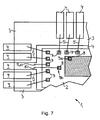
- the analysis contact is connected via a first connecting line with an encapsulant adjacent to the encapsulation, externally accessible terminal contact and this terminal contact via a second connecting line with a spaced from the terminal surface electrical connection point of the semiconductor chip, wherein the connecting lines so inside the Encapsulation mass are arranged so that the analysis contact can be separated during or after the removal of the encapsulant by area of the first connection line, without interrupting the second connection line.
- a predetermined electrical voltage may be applied to the externally accessible terminal contact and thus also to the analysis contact, for example the operating voltage or ground potential, such that the terminal area for the test signal is then at a defined potential. This allows a trouble-free operation of the semiconductor device.
- the electrical connection between the analysis contact and the connection contact is interrupted, so that then the actual test signal can be tapped on the analysis contact and / or fed into it.
- the connecting lines are preferably designed as bonding wires.
- the analysis contact projects transversely to the main extension plane of the semiconductor chip via a surface region of the semiconductor chip which adjoins the connection surface.
- the encapsulation compound can then be removed in regions to expose the analysis contact at the top of the semiconductor device.
- the analysis contact has at least two bonding sites stacked one above the other, perpendicular to the main extension plane of the semiconductor chip, and if at least one electrical connection point provided on the surface of the semiconductor chip is connected via a simple bonding site and / or a number stacked bonds, which is less than the number of stacked bonds of the analysis contact, is connected to a bonding wire.
- the analysis contact can then be applied to the semiconductor chip in a simple manner during the production of the semiconductor component in such a way that it projects beyond the bonding point arranged at the at least one connection point.
- the stacked bonding site is preferably designed as a so-called stacked ball bond.
- the analysis contact is further in contact with the surface of the semiconductor chip adjoining the connection surface than any other electrically conductive parts arranged in the interior of the encapsulation compound, which are electrically conductively connected to the semiconductor chip.
- the at least one analysis contact can then be made accessible in a simple manner by ablating a near-surface layer of the encapsulation compound over the whole surface for tapping and / or applying the test signal.
- the semiconductor chip has at least one first edge region and a second edge region extending transversely and / or parallel thereto, if the semiconductor chip has at least one connection point in the first edge region, which connects via a bonding wire embedded in the encapsulation compound to an externally accessible firing contact is, and in the second edge region no connection point is connected via a bonding wire with a.
- the at least one analysis contact can then be arranged in the second edge region or adjacent thereto.
- the analysis contact can be easily exposed by area-wise removal of encapsulant on the side of the semiconductor device, on which no bonding wires are provided.
- the semiconductor chip can be switched between an operating state and a test state as a function of an electrical voltage applied to the connection surface. It is even possible that in the test state analysis data and / or analysis signals from the semiconductor chip can be read via the externally accessible terminal contacts, which are locked in the operating state against reading. Thus, the semiconductor device can be further examined for possible errors.
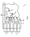
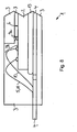
- An in Fig. 1 and 2 as a whole denoted by 1 semiconductor component has a semiconductor chip 2, in which an electrical circuit not shown in detail in the drawing is integrated.
- the semiconductor chip 2 is embedded in an electrically insulating encapsulation compound 3, which serves as a housing for the semiconductor chip 2.
- the encapsulation compound 3 is preferably made of plastic, with which the semiconductor chip 2 is encapsulated.
- connection contacts 4 which are connected via bonding wires 5 with connection points 7 arranged on the surface 6 of the semiconductor chip 2.
- the connection contacts 4 each have a molded with the encapsulant 3 first portion and a second portion which is exposed and accessible from the outside.
- the bonding wires 5 are connected in each case with their one end via a first bonding point with their associated connection point 7 of the semiconductor chip 2 and a second bonding point with its associated terminal 4 electrically conductive.
- the bonding wires 5 are completely in the interior of the potting compound at a distance from the outer surface.
- the semiconductor chip 2 also has on its surface 6 a plurality of pads 8 for test signals. On each pad 8, an analysis contact 9a, 9b is arranged, which projects beyond the surface 6 of the semiconductor chip 2.
- the supernatant can amount to at least 5%, in particular at least 10% and preferably at least 25%, of the wall thickness which the region of the encapsulation compound 3 adjoining the analysis contact 9a, 9b amounts to.
- the analysis contact 9a, 9b each consists of an electrically conductive material and is electrically connected to its associated pad 8.
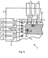
- Fig. 1 It can be seen that the analysis contacts 9a, 9b are arranged completely inside the encapsulation compound 3 at a distance from its outer surface. By ablating a near-surface layer of the encapsulation compound 3, the analysis contact 9a, 9b can be exposed.
- the removal of the encapsulation compound 3 can be effected by means of a mechanical tool, by the action of a chemical and / or by means of an energy beam.
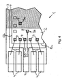
- Fig. 3 can be seen that the material removal is stopped as soon as a sufficiently large portion of the analysis contact 9a, 9b is exposed, which is adapted to be electrically contacted with a not shown in the drawing contact needle of an analyzer. Via the contact needle and the analysis contact 9a, 9b, the test signal at the connection surface 8 can then be tapped and / or fed into it in order to examine the electrical circuit, for example, after the occurrence of a defect on the semiconductor component 1. Below the region in which the encapsulation compound 3 has been removed, a sufficiently thick layer of the encapsulation compound 3 remains, via which the semiconductor chip 2 is furthermore electrically insulated and protected against mechanical damage and / or environmental influences.
- Fig. 3 can be seen that the encapsulant 3 is removed only over a portion of the surface 6 of the semiconductor chip 2. In a neighboring subarea surface 6, over which the bonding wires 5 are arranged, no material removal takes place. This avoids that the bonding wires are damaged when opening the semiconductor device 1.
- the analysis contact 9a is thus configured as a so-called stacked ball bond, ie it has two bonding sites stacked one above the other and perpendicular to the main extension plane of the semiconductor chip 2.
- the bonding wires 5 are connected to the connection points 7 only via simple bonding sites.
- the semiconductor chip 2 has edge regions 12a, 12b extending transversely to one another.
- first edge region 12a the connecting points 7 connected to the bonding wires 5 are arranged, and in a second edge region 12b no bonding wires 5 are provided.
- the region in which the encapsulation compound 3 is partially removed is located outside the first edge region 12.
- the region in which the encapsulation compound 3 is removed extends without interruption from an outer edge of the encapsulation compound 3 facing the second edge region 12b to a further one spaced therefrom Outer edge of the encapsulant 3.
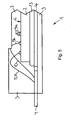
- connection contacts 4 which are connected via bonding wires 5 to connection points 7 of the semiconductor chip 2, at a plurality of edge regions extending transversely to each other. In this embodiment, the removal of material takes place at a distance from the outer edges of the encapsulation compound 3. It should also be mentioned that a connection contact 4 is connected via an adhesive layer 13 to the rear side of the semiconductor chip 2 facing away from the analysis contacts 9a, 9b.
Landscapes
- Engineering & Computer Science (AREA)
- Computer Hardware Design (AREA)
- Microelectronics & Electronic Packaging (AREA)
- Power Engineering (AREA)
- Manufacturing & Machinery (AREA)
- Physics & Mathematics (AREA)
- Condensed Matter Physics & Semiconductors (AREA)
- General Physics & Mathematics (AREA)
- Automation & Control Theory (AREA)
- Structures Or Materials For Encapsulating Or Coating Semiconductor Devices Or Solid State Devices (AREA)
- Testing Or Measuring Of Semiconductors Or The Like (AREA)
- Wire Bonding (AREA)
Claims (5)
- Composant semi-conducteur (1), avec au moins une puce semi-conductrice (2), dans laquelle un circuit électrique est intégré, dans lequel la puce semi-conductrice (2) présente au moins une face de raccordement (8) pour un signal de test, et dans lequel la puce semi-conductrice (2) est enveloppée par une masse d'enrobage (3) électriquement isolante recouvrant la face de raccordement (8) et présentant une surface extérieure, dans lequel la face de raccordement (8) est reliée de façon électriquement conductrice à un contact d'analyse (9a, 9b) disposé à l'intérieur de la masse d'enrobage (3) et saillant au-dessus de la surface (6) de la puce semi-conductrice (2), et le contact d'analyse (9a, 9b) est disposé à distance de la surface extérieure de la masse d'enrobage (3), caractérisé en ce qu'une partie du contact d'analyse (9a, 9b) est dénudée, dans lequel une couche suffisamment épaisse de la masse d'enrobage (3) est formée dans la région d'érosion sur la surface (b) de la puce semi-conductrice (2), et le contact d'analyse (9a, 9b) est relié par une première ligne de liaison (10) à un contact de raccordement (4) accessible de l'extérieur et adjacent à la masse d'enrobage (3) et ce contact de raccordement (4) est relié par une deuxième ligne de liaison (11) à un point de raccordement électrique (7) de la puce semi-conductrice (2) espacé de la face de raccordement (8), et en ce que les lignes de liaison (10, 11) sont disposées à l'intérieur de la masse d'enrobage (3) de telle manière que le contact d'analyse (9a, 9b) soit dénudé et qu'il soit séparé de la première ligne de liaison (10), sans interrompre la deuxième ligne de liaison (11).
- Composant semi-conducteur (1) selon la revendication 1, caractérisé en ce que le contact d'analyse (9a, 9b) est saillant au-dessus d'une région de la surface de la puce semi-conductrice (2) adjacente à la face de raccordement (8), transversalement au plan d'extension principal de la puce semi-conductrice (2).
- Composant semi-conducteur (1) selon la revendication 1 ou 2, caractérisé en ce que le contact d'analyse (9a, 9b) présente au moins deux points de jonction empilés l'un sur l'autre transversalement au plan d'extension principal de la puce semi-conductrice (2) et en ce qu'au moins un point de raccordement électrique (7) prévu sur la surface (6) de la puce semi-conductrice (2) est relié à un fil de jonction (5) par un simple point de jonction et/ou un nombre de points de jonction empilés l'un sur l'autre, qui est plus petit que le nombre des points de jonction du contact d'analyse (9a, 9b) empilés l'un sur l'autre.
- Composant semi-conducteur (1) selon l'une quelconque des revendications 1 à 3, caractérisé en ce que le contact d'analyse (9a, 9b) est davantage saillant au-dessus de la surface (6) de la puce semi-conductrice (2) adjacente à la face de contact (8) que toutes les autres parties électriquement conductrices disposées à l'intérieur de la masse d'enrobage (3), qui sont reliées de façon électriquement conductrice à la puce semi-conductrice (2).
- Composant semi-conducteur (1) selon l'une quelconque des revendications 1 à 4, caractérisé en ce que la puce semi-conductrice (2) présente au moins une première région de bord (12a) et une deuxième région de bord (12b) s'étendant transversalement et/ou parallèlement à celle-ci, en ce que la puce semi-conductrice (2) présente dans la première région de bord (12a) au moins un point de raccordement (7), qui est relié à au moins un contact de raccordement (4) accessible de l'extérieur par un fil de liaison (5) noyé dans la masse d'enrobage (3), et en ce qu'aucun point de raccordement dans la région de bord (12b) n'est relié à un contact de raccordement par un fil de liaison.
Priority Applications (3)
| Application Number | Priority Date | Filing Date | Title |
|---|---|---|---|
| EP07024487.6A EP2073262B1 (fr) | 2007-12-18 | 2007-12-18 | Composant semi-conducteur |
| JP2008316355A JP2009152592A (ja) | 2007-12-18 | 2008-12-12 | 半導体コンポーネント |
| US12/336,862 US8125070B2 (en) | 2007-12-18 | 2008-12-17 | Semiconductor component |
Applications Claiming Priority (1)
| Application Number | Priority Date | Filing Date | Title |
|---|---|---|---|
| EP07024487.6A EP2073262B1 (fr) | 2007-12-18 | 2007-12-18 | Composant semi-conducteur |
Publications (2)
| Publication Number | Publication Date |
|---|---|
| EP2073262A1 EP2073262A1 (fr) | 2009-06-24 |
| EP2073262B1 true EP2073262B1 (fr) | 2015-09-30 |
Family
ID=39310983
Family Applications (1)
| Application Number | Title | Priority Date | Filing Date |
|---|---|---|---|
| EP07024487.6A Ceased EP2073262B1 (fr) | 2007-12-18 | 2007-12-18 | Composant semi-conducteur |
Country Status (3)
| Country | Link |
|---|---|
| US (1) | US8125070B2 (fr) |
| EP (1) | EP2073262B1 (fr) |
| JP (1) | JP2009152592A (fr) |
Families Citing this family (3)
| Publication number | Priority date | Publication date | Assignee | Title |
|---|---|---|---|---|
| DE102011003870A1 (de) * | 2011-02-09 | 2012-08-09 | Robert Bosch Gmbh | Schaltungsmodul für ein Fahrzeug |
| DE102014215332A1 (de) * | 2014-08-04 | 2016-02-04 | Zf Friedrichshafen Ag | Verfahren zur Vorbereitung einer Leiterplatte für eine Funktionsprüfung |
| US10103072B2 (en) * | 2016-08-18 | 2018-10-16 | Semiconductor Components Industries, Llc | Damaging components with defective electrical couplings |
Citations (1)
| Publication number | Priority date | Publication date | Assignee | Title |
|---|---|---|---|---|
| JP2002305265A (ja) * | 2001-04-05 | 2002-10-18 | Mitsubishi Electric Corp | 試験用端子内蔵半導体装置およびその試験方法 |
Family Cites Families (11)
| Publication number | Priority date | Publication date | Assignee | Title |
|---|---|---|---|---|
| JP2721151B2 (ja) | 1986-04-01 | 1998-03-04 | 株式会社東芝 | 半導体集積回路装置 |
| JP2738568B2 (ja) | 1989-09-06 | 1998-04-08 | 新光電気工業株式会社 | 半導体チップモジュール |
| SG111023A1 (en) | 2001-07-11 | 2005-05-30 | Inst Data Storage | Method and apparatus for decapping integrated circuit packages |
| EP1440608B1 (fr) | 2001-11-02 | 2006-02-15 | ATMEL Germany GmbH | Procede pour ouvrir le boitier en plastique d'un module electronique |
| JP2003347482A (ja) | 2002-05-28 | 2003-12-05 | Konica Minolta Holdings Inc | 半導体パッケージ、半導体パッケージの製造方法及び半導体パッケージの検査方法 |
| US6815254B2 (en) * | 2003-03-10 | 2004-11-09 | Freescale Semiconductor, Inc. | Semiconductor package with multiple sides having package contacts |
| KR100574947B1 (ko) * | 2003-08-20 | 2006-05-02 | 삼성전자주식회사 | Bga 패키지, 그 제조방법 및 bga 패키지 적층 구조 |
| US7259028B2 (en) | 2005-12-29 | 2007-08-21 | Sandisk Corporation | Test pads on flash memory cards |
| US7385299B2 (en) | 2006-02-25 | 2008-06-10 | Stats Chippac Ltd. | Stackable integrated circuit package system with multiple interconnect interface |
| TWI327769B (en) * | 2006-12-29 | 2010-07-21 | Ind Tech Res Inst | A packaging structure of pressure sensor and a method therefor |
| US20080315436A1 (en) * | 2007-06-20 | 2008-12-25 | Broadcom Corporation | Semiconductor wafer that supports multiple packaging techniques |
-
2007
- 2007-12-18 EP EP07024487.6A patent/EP2073262B1/fr not_active Ceased
-
2008
- 2008-12-12 JP JP2008316355A patent/JP2009152592A/ja active Pending
- 2008-12-17 US US12/336,862 patent/US8125070B2/en not_active Expired - Fee Related
Patent Citations (1)
| Publication number | Priority date | Publication date | Assignee | Title |
|---|---|---|---|---|
| JP2002305265A (ja) * | 2001-04-05 | 2002-10-18 | Mitsubishi Electric Corp | 試験用端子内蔵半導体装置およびその試験方法 |
Also Published As
| Publication number | Publication date |
|---|---|
| JP2009152592A (ja) | 2009-07-09 |
| US20090152548A1 (en) | 2009-06-18 |
| EP2073262A1 (fr) | 2009-06-24 |
| US8125070B2 (en) | 2012-02-28 |
Similar Documents
| Publication | Publication Date | Title |
|---|---|---|
| DE2554965C2 (fr) | ||
| DE102014100512B4 (de) | Chip-gehäuse mit anschlusspads mit unterschiedlichen formfaktoren | |
| DE102013113186B4 (de) | Halbleiterpackage und Verfahren für dessen Ausbildung | |
| DE3814469C2 (fr) | ||
| DE102014100509B4 (de) | Verfahren zur herstellung und testung eines chipgehäuses | |
| DE102009055882A1 (de) | Leistungshalbleitervorrichtung | |
| DE102005047414A1 (de) | Magnetoresistives Sensormodul und Verfahren zum Herstellen desselben | |
| DE69737320T2 (de) | Halbleitervorrichtung | |
| DE112014003204B4 (de) | Leistungsmodul | |
| DE102007041785A1 (de) | Halbleitervorrichtung und deren Herstellungsverfahren | |
| EP2073262B1 (fr) | Composant semi-conducteur | |
| DE19526511A1 (de) | Halbleitervorrichtung und Verfahren zu deren Herstellung und Montage | |
| DE102004027960B4 (de) | Elektrische Leistungs-Halbleitervorrichtung | |
| DE19962702A1 (de) | Prüfsockel einer BGA-Vorrichtung | |
| DE69609921T2 (de) | Herstellungsverfahren einer halbleiteranordnung geeignet zur oberflächenmontage | |
| DE10060585A1 (de) | Vorrichtung und Verfahren zur Untersuchung einer integrierten Halbleiterschaltung | |
| DE10213609B4 (de) | Elektrisches Bauelement mit einer Kontaktierungsfläche und Verfahren zum Ausbilden einer Kontaktierungsfläche auf einem Halbleitermaterial | |
| DE102006045415A1 (de) | Bauelementanordnung mit einem Träger | |
| DE102007036566A1 (de) | Federkontaktierung von elektrischen Kontaktflächen eines elektronischen Bauteils | |
| DE10028145A1 (de) | Integrierte Schaltungsanordnung zum Testen von Transistoren | |
| DE102010008618A1 (de) | Halbleitervorrichtung | |
| DE102004010299B4 (de) | Infrarot-Empfänger-Chip | |
| DE10339022A1 (de) | Halbleitervorrichtung | |
| DE10223722A1 (de) | Halbleitervorrichtung | |
| DE19861009B4 (de) | Halbleitereinrichtung |
Legal Events
| Date | Code | Title | Description |
|---|---|---|---|
| PUAI | Public reference made under article 153(3) epc to a published international application that has entered the european phase |
Free format text: ORIGINAL CODE: 0009012 |
|
| AK | Designated contracting states |
Kind code of ref document: A1 Designated state(s): AT BE BG CH CY CZ DE DK EE ES FI FR GB GR HU IE IS IT LI LT LU LV MC MT NL PL PT RO SE SI SK TR |
|
| AX | Request for extension of the european patent |
Extension state: AL BA HR MK RS |
|
| 17P | Request for examination filed |
Effective date: 20090626 |
|
| AKX | Designation fees paid |
Designated state(s): DE FR GB |
|
| 17Q | First examination report despatched |
Effective date: 20110316 |
|
| GRAP | Despatch of communication of intention to grant a patent |
Free format text: ORIGINAL CODE: EPIDOSNIGR1 |
|
| INTG | Intention to grant announced |
Effective date: 20150423 |
|
| RIN1 | Information on inventor provided before grant (corrected) |
Inventor name: HEBERLE, KLAUS Inventor name: BIDENBACH, REINER Inventor name: SCHUBERT, JENS Inventor name: KREDLER, STEFAN |
|
| GRAS | Grant fee paid |
Free format text: ORIGINAL CODE: EPIDOSNIGR3 |
|
| GRAA | (expected) grant |
Free format text: ORIGINAL CODE: 0009210 |
|
| AK | Designated contracting states |
Kind code of ref document: B1 Designated state(s): DE FR GB |
|
| REG | Reference to a national code |
Ref country code: GB Ref legal event code: FG4D Free format text: NOT ENGLISH |
|
| REG | Reference to a national code |
Ref country code: DE Ref legal event code: R096 Ref document number: 502007014261 Country of ref document: DE |
|
| REG | Reference to a national code |
Ref country code: FR Ref legal event code: PLFP Year of fee payment: 9 |
|
| REG | Reference to a national code |
Ref country code: DE Ref legal event code: R097 Ref document number: 502007014261 Country of ref document: DE |
|
| PLBE | No opposition filed within time limit |
Free format text: ORIGINAL CODE: 0009261 |
|
| STAA | Information on the status of an ep patent application or granted ep patent |
Free format text: STATUS: NO OPPOSITION FILED WITHIN TIME LIMIT |
|
| 26N | No opposition filed |
Effective date: 20160701 |
|
| REG | Reference to a national code |
Ref country code: FR Ref legal event code: PLFP Year of fee payment: 10 |
|
| REG | Reference to a national code |
Ref country code: DE Ref legal event code: R082 Ref document number: 502007014261 Country of ref document: DE Representative=s name: KOCH-MUELLER PATENTANWALTSGESELLSCHAFT MBH, DE Ref country code: DE Ref legal event code: R081 Ref document number: 502007014261 Country of ref document: DE Owner name: TDK-MICRONAS GMBH, DE Free format text: FORMER OWNER: MICRONAS GMBH, 79108 FREIBURG, DE |
|
| REG | Reference to a national code |
Ref country code: FR Ref legal event code: PLFP Year of fee payment: 11 |
|
| REG | Reference to a national code |
Ref country code: FR Ref legal event code: CD Owner name: TDK-MICRONAS GMBH, DE Effective date: 20180717 |
|
| PGFP | Annual fee paid to national office [announced via postgrant information from national office to epo] |
Ref country code: FR Payment date: 20181220 Year of fee payment: 12 Ref country code: GB Payment date: 20181218 Year of fee payment: 12 |
|
| GBPC | Gb: european patent ceased through non-payment of renewal fee |
Effective date: 20191218 |
|
| PG25 | Lapsed in a contracting state [announced via postgrant information from national office to epo] |
Ref country code: FR Free format text: LAPSE BECAUSE OF NON-PAYMENT OF DUE FEES Effective date: 20191231 Ref country code: GB Free format text: LAPSE BECAUSE OF NON-PAYMENT OF DUE FEES Effective date: 20191218 |
|
| PGFP | Annual fee paid to national office [announced via postgrant information from national office to epo] |
Ref country code: DE Payment date: 20211210 Year of fee payment: 15 |
|
| REG | Reference to a national code |
Ref country code: DE Ref legal event code: R119 Ref document number: 502007014261 Country of ref document: DE |
|
| PG25 | Lapsed in a contracting state [announced via postgrant information from national office to epo] |
Ref country code: DE Free format text: LAPSE BECAUSE OF NON-PAYMENT OF DUE FEES Effective date: 20230701 |