EP2071394A1 - Active matrix substrate and liquid crystal display device provided with same - Google Patents
Active matrix substrate and liquid crystal display device provided with same Download PDFInfo
- Publication number
- EP2071394A1 EP2071394A1 EP07742948A EP07742948A EP2071394A1 EP 2071394 A1 EP2071394 A1 EP 2071394A1 EP 07742948 A EP07742948 A EP 07742948A EP 07742948 A EP07742948 A EP 07742948A EP 2071394 A1 EP2071394 A1 EP 2071394A1
- Authority
- EP
- European Patent Office
- Prior art keywords
- electrodes
- common electrode
- wires
- active matrix
- matrix substrate
- Prior art date
- Legal status (The legal status is an assumption and is not a legal conclusion. Google has not performed a legal analysis and makes no representation as to the accuracy of the status listed.)
- Granted
Links
Images






Classifications
-
- G—PHYSICS
- G02—OPTICS
- G02F—OPTICAL DEVICES OR ARRANGEMENTS FOR THE CONTROL OF LIGHT BY MODIFICATION OF THE OPTICAL PROPERTIES OF THE MEDIA OF THE ELEMENTS INVOLVED THEREIN; NON-LINEAR OPTICS; FREQUENCY-CHANGING OF LIGHT; OPTICAL LOGIC ELEMENTS; OPTICAL ANALOGUE/DIGITAL CONVERTERS
- G02F1/00—Devices or arrangements for the control of the intensity, colour, phase, polarisation or direction of light arriving from an independent light source, e.g. switching, gating or modulating; Non-linear optics
- G02F1/01—Devices or arrangements for the control of the intensity, colour, phase, polarisation or direction of light arriving from an independent light source, e.g. switching, gating or modulating; Non-linear optics for the control of the intensity, phase, polarisation or colour
- G02F1/13—Devices or arrangements for the control of the intensity, colour, phase, polarisation or direction of light arriving from an independent light source, e.g. switching, gating or modulating; Non-linear optics for the control of the intensity, phase, polarisation or colour based on liquid crystals, e.g. single liquid crystal display cells
- G02F1/133—Constructional arrangements; Operation of liquid crystal cells; Circuit arrangements
- G02F1/1333—Constructional arrangements; Manufacturing methods
- G02F1/1343—Electrodes
- G02F1/134309—Electrodes characterised by their geometrical arrangement
- G02F1/134363—Electrodes characterised by their geometrical arrangement for applying an electric field parallel to the substrate, i.e. in-plane switching [IPS]
-
- G—PHYSICS
- G02—OPTICS
- G02F—OPTICAL DEVICES OR ARRANGEMENTS FOR THE CONTROL OF LIGHT BY MODIFICATION OF THE OPTICAL PROPERTIES OF THE MEDIA OF THE ELEMENTS INVOLVED THEREIN; NON-LINEAR OPTICS; FREQUENCY-CHANGING OF LIGHT; OPTICAL LOGIC ELEMENTS; OPTICAL ANALOGUE/DIGITAL CONVERTERS
- G02F1/00—Devices or arrangements for the control of the intensity, colour, phase, polarisation or direction of light arriving from an independent light source, e.g. switching, gating or modulating; Non-linear optics
- G02F1/01—Devices or arrangements for the control of the intensity, colour, phase, polarisation or direction of light arriving from an independent light source, e.g. switching, gating or modulating; Non-linear optics for the control of the intensity, phase, polarisation or colour
- G02F1/13—Devices or arrangements for the control of the intensity, colour, phase, polarisation or direction of light arriving from an independent light source, e.g. switching, gating or modulating; Non-linear optics for the control of the intensity, phase, polarisation or colour based on liquid crystals, e.g. single liquid crystal display cells
- G02F1/133—Constructional arrangements; Operation of liquid crystal cells; Circuit arrangements
- G02F1/136—Liquid crystal cells structurally associated with a semi-conducting layer or substrate, e.g. cells forming part of an integrated circuit
- G02F1/13606—Liquid crystal cells structurally associated with a semi-conducting layer or substrate, e.g. cells forming part of an integrated circuit having means for reducing parasitic capacitance
-
- G—PHYSICS
- G02—OPTICS
- G02F—OPTICAL DEVICES OR ARRANGEMENTS FOR THE CONTROL OF LIGHT BY MODIFICATION OF THE OPTICAL PROPERTIES OF THE MEDIA OF THE ELEMENTS INVOLVED THEREIN; NON-LINEAR OPTICS; FREQUENCY-CHANGING OF LIGHT; OPTICAL LOGIC ELEMENTS; OPTICAL ANALOGUE/DIGITAL CONVERTERS
- G02F1/00—Devices or arrangements for the control of the intensity, colour, phase, polarisation or direction of light arriving from an independent light source, e.g. switching, gating or modulating; Non-linear optics
- G02F1/01—Devices or arrangements for the control of the intensity, colour, phase, polarisation or direction of light arriving from an independent light source, e.g. switching, gating or modulating; Non-linear optics for the control of the intensity, phase, polarisation or colour
- G02F1/13—Devices or arrangements for the control of the intensity, colour, phase, polarisation or direction of light arriving from an independent light source, e.g. switching, gating or modulating; Non-linear optics for the control of the intensity, phase, polarisation or colour based on liquid crystals, e.g. single liquid crystal display cells
- G02F1/133—Constructional arrangements; Operation of liquid crystal cells; Circuit arrangements
- G02F1/136—Liquid crystal cells structurally associated with a semi-conducting layer or substrate, e.g. cells forming part of an integrated circuit
- G02F1/1362—Active matrix addressed cells
- G02F1/136227—Through-hole connection of the pixel electrode to the active element through an insulation layer
-
- G—PHYSICS
- G02—OPTICS
- G02F—OPTICAL DEVICES OR ARRANGEMENTS FOR THE CONTROL OF LIGHT BY MODIFICATION OF THE OPTICAL PROPERTIES OF THE MEDIA OF THE ELEMENTS INVOLVED THEREIN; NON-LINEAR OPTICS; FREQUENCY-CHANGING OF LIGHT; OPTICAL LOGIC ELEMENTS; OPTICAL ANALOGUE/DIGITAL CONVERTERS
- G02F1/00—Devices or arrangements for the control of the intensity, colour, phase, polarisation or direction of light arriving from an independent light source, e.g. switching, gating or modulating; Non-linear optics
- G02F1/01—Devices or arrangements for the control of the intensity, colour, phase, polarisation or direction of light arriving from an independent light source, e.g. switching, gating or modulating; Non-linear optics for the control of the intensity, phase, polarisation or colour
- G02F1/13—Devices or arrangements for the control of the intensity, colour, phase, polarisation or direction of light arriving from an independent light source, e.g. switching, gating or modulating; Non-linear optics for the control of the intensity, phase, polarisation or colour based on liquid crystals, e.g. single liquid crystal display cells
- G02F1/133—Constructional arrangements; Operation of liquid crystal cells; Circuit arrangements
- G02F1/136—Liquid crystal cells structurally associated with a semi-conducting layer or substrate, e.g. cells forming part of an integrated circuit
- G02F1/1362—Active matrix addressed cells
- G02F1/136259—Repairing; Defects
- G02F1/136263—Line defects
-
- G—PHYSICS
- G02—OPTICS
- G02F—OPTICAL DEVICES OR ARRANGEMENTS FOR THE CONTROL OF LIGHT BY MODIFICATION OF THE OPTICAL PROPERTIES OF THE MEDIA OF THE ELEMENTS INVOLVED THEREIN; NON-LINEAR OPTICS; FREQUENCY-CHANGING OF LIGHT; OPTICAL LOGIC ELEMENTS; OPTICAL ANALOGUE/DIGITAL CONVERTERS
- G02F1/00—Devices or arrangements for the control of the intensity, colour, phase, polarisation or direction of light arriving from an independent light source, e.g. switching, gating or modulating; Non-linear optics
- G02F1/01—Devices or arrangements for the control of the intensity, colour, phase, polarisation or direction of light arriving from an independent light source, e.g. switching, gating or modulating; Non-linear optics for the control of the intensity, phase, polarisation or colour
- G02F1/13—Devices or arrangements for the control of the intensity, colour, phase, polarisation or direction of light arriving from an independent light source, e.g. switching, gating or modulating; Non-linear optics for the control of the intensity, phase, polarisation or colour based on liquid crystals, e.g. single liquid crystal display cells
- G02F1/133—Constructional arrangements; Operation of liquid crystal cells; Circuit arrangements
- G02F1/136—Liquid crystal cells structurally associated with a semi-conducting layer or substrate, e.g. cells forming part of an integrated circuit
- G02F1/1362—Active matrix addressed cells
- G02F1/136286—Wiring, e.g. gate line, drain line
- G02F1/13629—Multilayer wirings
-
- G—PHYSICS
- G02—OPTICS
- G02F—OPTICAL DEVICES OR ARRANGEMENTS FOR THE CONTROL OF LIGHT BY MODIFICATION OF THE OPTICAL PROPERTIES OF THE MEDIA OF THE ELEMENTS INVOLVED THEREIN; NON-LINEAR OPTICS; FREQUENCY-CHANGING OF LIGHT; OPTICAL LOGIC ELEMENTS; OPTICAL ANALOGUE/DIGITAL CONVERTERS
- G02F1/00—Devices or arrangements for the control of the intensity, colour, phase, polarisation or direction of light arriving from an independent light source, e.g. switching, gating or modulating; Non-linear optics
- G02F1/01—Devices or arrangements for the control of the intensity, colour, phase, polarisation or direction of light arriving from an independent light source, e.g. switching, gating or modulating; Non-linear optics for the control of the intensity, phase, polarisation or colour
- G02F1/13—Devices or arrangements for the control of the intensity, colour, phase, polarisation or direction of light arriving from an independent light source, e.g. switching, gating or modulating; Non-linear optics for the control of the intensity, phase, polarisation or colour based on liquid crystals, e.g. single liquid crystal display cells
- G02F1/133—Constructional arrangements; Operation of liquid crystal cells; Circuit arrangements
- G02F1/136—Liquid crystal cells structurally associated with a semi-conducting layer or substrate, e.g. cells forming part of an integrated circuit
- G02F1/1362—Active matrix addressed cells
- G02F1/1368—Active matrix addressed cells in which the switching element is a three-electrode device
-
- H—ELECTRICITY
- H10—SEMICONDUCTOR DEVICES; ELECTRIC SOLID-STATE DEVICES NOT OTHERWISE PROVIDED FOR
- H10D—INORGANIC ELECTRIC SEMICONDUCTOR DEVICES
- H10D86/00—Integrated devices formed in or on insulating or conducting substrates, e.g. formed in silicon-on-insulator [SOI] substrates or on stainless steel or glass substrates
- H10D86/40—Integrated devices formed in or on insulating or conducting substrates, e.g. formed in silicon-on-insulator [SOI] substrates or on stainless steel or glass substrates characterised by multiple TFTs
-
- H—ELECTRICITY
- H10—SEMICONDUCTOR DEVICES; ELECTRIC SOLID-STATE DEVICES NOT OTHERWISE PROVIDED FOR
- H10D—INORGANIC ELECTRIC SEMICONDUCTOR DEVICES
- H10D86/00—Integrated devices formed in or on insulating or conducting substrates, e.g. formed in silicon-on-insulator [SOI] substrates or on stainless steel or glass substrates
- H10D86/40—Integrated devices formed in or on insulating or conducting substrates, e.g. formed in silicon-on-insulator [SOI] substrates or on stainless steel or glass substrates characterised by multiple TFTs
- H10D86/441—Interconnections, e.g. scanning lines
-
- G—PHYSICS
- G02—OPTICS
- G02F—OPTICAL DEVICES OR ARRANGEMENTS FOR THE CONTROL OF LIGHT BY MODIFICATION OF THE OPTICAL PROPERTIES OF THE MEDIA OF THE ELEMENTS INVOLVED THEREIN; NON-LINEAR OPTICS; FREQUENCY-CHANGING OF LIGHT; OPTICAL LOGIC ELEMENTS; OPTICAL ANALOGUE/DIGITAL CONVERTERS
- G02F2201/00—Constructional arrangements not provided for in groups G02F1/00 - G02F7/00
- G02F2201/12—Constructional arrangements not provided for in groups G02F1/00 - G02F7/00 electrode
- G02F2201/121—Constructional arrangements not provided for in groups G02F1/00 - G02F7/00 electrode common or background
-
- H—ELECTRICITY
- H10—SEMICONDUCTOR DEVICES; ELECTRIC SOLID-STATE DEVICES NOT OTHERWISE PROVIDED FOR
- H10D—INORGANIC ELECTRIC SEMICONDUCTOR DEVICES
- H10D86/00—Integrated devices formed in or on insulating or conducting substrates, e.g. formed in silicon-on-insulator [SOI] substrates or on stainless steel or glass substrates
- H10D86/40—Integrated devices formed in or on insulating or conducting substrates, e.g. formed in silicon-on-insulator [SOI] substrates or on stainless steel or glass substrates characterised by multiple TFTs
- H10D86/451—Integrated devices formed in or on insulating or conducting substrates, e.g. formed in silicon-on-insulator [SOI] substrates or on stainless steel or glass substrates characterised by multiple TFTs characterised by the compositions or shapes of the interlayer dielectrics
-
- H—ELECTRICITY
- H10—SEMICONDUCTOR DEVICES; ELECTRIC SOLID-STATE DEVICES NOT OTHERWISE PROVIDED FOR
- H10D—INORGANIC ELECTRIC SEMICONDUCTOR DEVICES
- H10D86/00—Integrated devices formed in or on insulating or conducting substrates, e.g. formed in silicon-on-insulator [SOI] substrates or on stainless steel or glass substrates
- H10D86/40—Integrated devices formed in or on insulating or conducting substrates, e.g. formed in silicon-on-insulator [SOI] substrates or on stainless steel or glass substrates characterised by multiple TFTs
- H10D86/60—Integrated devices formed in or on insulating or conducting substrates, e.g. formed in silicon-on-insulator [SOI] substrates or on stainless steel or glass substrates characterised by multiple TFTs wherein the TFTs are in active matrices
Definitions
- the present invention relates to an active matrix substrate which incorporates a TFT, and a liquid crystal display device including the active matrix substrate.
- a liquid crystal display device of the FFS mode is arranged such that a counter electrode and a pixel electrode (i) are formed by transparent material such as ITO, (ii) have a narrower space between the counter electrode and the pixel electrode than a space between the upper and lower substrates, and further (iii) have a width between the counter electrode and the pixel electrode in a degree in which all of liquid molecules aligned on an upper part of an electrode are drivable.
- a counter electrode and a pixel electrode are formed by transparent material such as ITO, (ii) have a narrower space between the counter electrode and the pixel electrode than a space between the upper and lower substrates, and further (iii) have a width between the counter electrode and the pixel electrode in a degree in which all of liquid molecules aligned on an upper part of an electrode are drivable.
- the liquid crystal display device of the FFS mode can attain a higher aperture ratio than that of a liquid crystal display device of an IPS (In-Place-Switching) mode, since the electrodes and the like are formed by the transparent material. That is to say, a higher aperture ratio than that of the IPS mode is attainable by causing light transmission to occur at an electrode section.
- IPS In-Place-Switching
- FIG. 21 (a) is a plane view of an active matrix substrate to be used in a liquid crystal display device of the FFS mode, as described in Patent Document 1, and (b) is a cross sectional view taken on line A-A' indicated in (a) of Fig. 21 .
- the active matrix substrate mainly includes: a plurality of gate bus lines 101 and a plurality of source bus lines 107 which orthogonally intersect with each other; a plurality of pixel electrodes 109 provided comblike and parallel to the source bus lines 107 in pixel areas surrounded by the gate and source bus lines, respectively; TFTs 103 provided on sections in which the gate bus lines 101 diverge to the pixel area side; and common electrode wires (CS wires) 110 provided parallel to the gate bus lines 101.
- CS wires common electrode wires
- the active matrix substrate has common electrodes (gate bus line lower layer) 106 which consist of a transparent conductive film on an insulating substrate. Further, on the common electrodes 106 are provided a gate bus line upper layer 101 and CS wires 110. Moreover, a semiconductor layer 103, a contact layer 104, and a source/drain electrode upper layer 107 are stacked on the gate bus line upper layer 101 sandwiching a gate insulating film 102 between the semiconductor layer 103 and the gate bus line upper layer 101, so as to form a TFT. On an uppermost layer of the active matrix substrate is provided pixel electrodes 109 via an interlayer insulating film (passivation film) 108.
- the active matrix substrate described in Patent Document 1 has the following two problems, caused by the common electrodes which form the CS wires 110 being provided on the gate bus line lower layer 106.
- roughening of the common electrodes and the gate bus line upper layer causes the semiconductor layer 103, the contact layer 104, and the source/drain electrode upper layer 107 that are provided on the gate insulating film 102 to also roughen.
- the semiconductor layer 103, the contact layer 104, and the source/drain electrode upper layer 107 form a channel section 111 of the TFT.
- the flatness becomes low. This causes the roughness of the channel section 111 of the TFT to increase. As a result, a problem of a decrease in mobility occurs.
- the transparent electrodes have an extremely low transition temperature of crystallization, that is, the transparent electrodes polysiliconize (crystallize) from an amorphous state at around a temperature in a range of 150 ° to 200 °.
- the transparent electrodes are compared between a crystallized state and the amorphous state, a large difference is recognized in an etching rate. Therefore, polysiliconization of the transparent electrodes causes a need to etch for a remarkably long period of time. Namely, as illustrated in Fig. 23 , over-etching is required.
- the gate bus lines 101 become back tapered (peaked), and the gate insulating film 102 cannot cover the gate bus lines 101. This causes a problem that an efficiency percentage decreases, such as occurrence of leaking from the metal thin film formed on the upper layer.
- An active matrix substrate described in Patent Document 2 provides common electrodes on a gate insulating film.
- the common electrodes are provided on a layer upper than the gate bus lines. Therefore, the two aforementioned problems are solved.
- Patent Documents 1 and 2 both form the common electrodes parallel to the gate bus lines by use of a metal layer of the gate bus lines arranged horizontally to the liquid crystal display section. That is to say, the CS wires 123 are horizontally provided, as illustrated in Fig. 24 .
- the gate bus lines are longer as compared to the source bus lines. Consequently, the common electrodes formed at the CS wires 123 have a high resistance, which causes a problem of signal delay.
- a width of the CS wires 123 is thickened so as to aim for low resistance, another problem occurs that an aperture ratio decreases.
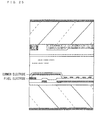
- Patent Document 3 provides the common electrodes (transparent electrode material, for example ITO) on a further upper position than the pixel electrodes, as illustrated in Fig. 25 .
- the transparent electrode material is left remaining on all of an area except for a slit section of the common electrodes, so as to form the common electrodes.
- the transparent electrode material (CS wires) is provided on substantially the entire source bus lines and gate bus lines. As such, the problem of signal delay is solved by providing the CS wires parallel to the source bus lines.
- the CS wires are formed so as to cover the entire source bus lines and gate bus lines illustrated in Fig. 26 . Therefore, defects such as a shortage and the like may possibly occur, and a parasitic capacitance between the gate and source bus lines and the CS wires increases.
- the present invention is attained in view of the problems, and its purpose is to provide an active matrix substrate and a liquid crystal display device including the same that has small signal delay caused by resistance and small signal delay caused by parasitic capacitance.
- an active matrix substrate of the present invention includes an insulating substrate; video signal lines and scanning signal lines provided orthogonally intersecting with each other on the insulating substrate; and thin film transistors provided at intersections of the video signal lines and the scanning signal lines, the thin film transistors including gate electrodes, source electrodes, and drain electrodes, respectively, a transparent electrode layer, formed to be used as a lower layer of the source electrodes and the drain electrodes, being used as (i) common electrodes provided in pixel areas surrounded by adjacent video signal lines and adjacent scanning signal lines, respectively and (ii) common electrode wires for connecting adjacent ones of the common electrodes parallel to the video signal lines.
- a transparent electrode layer that is formed to be used as a lower layer of source electrodes and drain electrodes is used as (i) common electrodes provided in pixel areas surrounded by adjacent video signal lines and adjacent scanning signal lines, respectively and (ii) common electrode wires for connecting adjacent ones of the common electrodes parallel to the video signal lines.
- the common electrodes and the common electrode wires are formed by use of the transparent electrode layer that is to be used as a lower layer of the source electrodes and the drain electrodes. This allows the common electrodes to be connected and extended in a parallel direction to the video signal lines that are connected to the source electrodes.
- video signal lines are shorter than the scanning signal lines. Therefore, it is possible to reduce resistance as compared to the common electrodes being extended parallel to the scanning signal lines.
- the common electrode wires do not have any part overlapping with the video signal lines, and are formed so as to overlap at a part where the common electrode wires orthogonally intersect with the scanning signal lines.
- the present invention reduces the resistance of the common electrodes and the common electrode wires, as well as reducing the parasitic capacitance between the common electrode wires and the signal lines. Therefore, it is possible to reduce the signal delay of the common electrode wires.
- a transparent electrode layer transparent conductive material such as ITO
- ITO transparent conductive material
- the active matrix substrate of the present invention is preferably arranged such that a metal film formed so as to create the gate electrodes is used as auxiliary common electrode wires that are provided parallel to the scanning signal lines, and the auxiliary common electrode wires and the common electrodes are electrically connected to each other via contact holes, respectively.
- auxiliary common electrode wires are provided parallel to the scanning signal lines, and the auxiliary common electrode wires and the common electrodes are electrically connected to each other via contact holes, respectively, provided on the gate insulating film. That is to say, a reticulate structure is formed by use of the common electrodes, common electrode wires and the auxiliary common electrode wires. Therefore, it is possible to have the structure close to one which a resistance is determined just by a relation of an aspect ratio (concept of sheet resistance), regardless of its size and material. Therefore, it is possible to reduce the resistance between two arbitrary points.
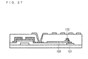
- the common electrodes 120 and the common electrode wires 121 are connected to each other via source metals (metal layer of source bus lines) as illustrated in Fig. 27 .
- source metals metal layer of source bus lines
- the reticulate structure enables the common electrodes to have four-directional redundancy. Therefore, even if a pixel that cannot make the ohmic contact, or, further even if one of the common electrodes and/or the auxiliary common electrodes have a breakage, the pixel defect and line defect is prevented to the utmost.
- each of the common electrodes has an opening section whose first and second end sections are located outside and inside, respectively, of an outer edge of a respective one of the contact holes; and contact electrode pads connected to (i) the auxiliary common electrode wires on the first end sections side of the common electrodes, and (ii) the common electrodes on the second end sections side of the common electrodes, respectively.
- each of the common electrodes has an opening whose first and second end sections are located outside and inside, respectively, of an outer edge of a respective one of the contact holes, and contact electrode pads are connected to (i) the auxiliary common electrode wires on the first end sections side of the common electrodes, and (ii) the common electrodes on the second end sections side of the common electrodes, respectively.
- This allows electrical connection between the common electrodes and the auxiliary common electrode wires by use of the contact electrode pads.
- this allows elimination of a contact hole forming step for connecting the common electrodes and the auxiliary common electrode wires, which forming step is to be carried out before formation of the source wires/electrodes and the drain electrodes.
- the active matrix substrate of the present invention is preferably arranged such that the pixel areas include pixel electrodes, and the contact electrode pads are formed to be made of a same material and in a same manufacturing step as the pixel electrodes.
- pixel electrodes and contact pads are formed by a same material and in a same manufacturing step. This allows simplification of a manufacturing method.
- the active matrix substrate of the present invention is preferably arranged such that the auxiliary common electrode wires are provided substantially mid between adjacent ones of the scanning signal lines, respectively.
- the auxiliary common electrode wires are provided substantially mid between adjacent ones of the scanning signal lines.
- the auxiliary common electrode wires are provided parallel to the scanning signal lines. Therefore, by providing the auxiliary common electrode wires substantially mid between the adjacent ones of the scanning signal lines, a distance between the auxiliary common electrode wires and the scanning signal lines is maximized. A longer distance from the auxiliary common electrode wires to the scanning signal line reduces a possibility of a shortage in the auxiliary common electrode wires and the scanning signal lines due to poor patterns and adherence of dust.
- the active matrix substrate of the present invention is preferably arranged such that the auxiliary common electrode wires are provided in a vicinity of one of adjacent ones of the scanning signal lines.
- the auxiliary common electrode wires are provided in a vicinity of one of the adjacent ones of the scanning signal lines.
- the vicinity of the scanning signal lines is an area that does not contribute to an aperture. Therefore, it is possible to realize a high aperture ratio since parts of the auxiliary common electrode wires are provided on the area which does not contribute to the aperture.
- the active matrix substrate of the present invention is preferably arranged such that the auxiliary common electrode wires extend to outer peripheral sections of the common electrodes, and extend in the outer peripheral sections so as to be parallel to the video signal lines, respectively.
- the outer peripheral section of the common electrode has a so-called disabled area (an area in which liquid crystal does not move, and a liquid crystal domain occurrence area).
- the auxiliary common electrode wires extend to the outer peripheral section of the common electrodes and extend in the outer peripheral sections so as to be parallel to the video signal lines, respectively. Therefore, light shielding of the disabled area is carried out by the auxiliary common electrode wires, therefore allows attainment of a high display quality.
- the active matrix substrate of the present invention is preferably arranged such that the auxiliary common electrode wires also extend to the outer peripheral sections of the common electrodes, and extend in the outer peripheral sections so as to be parallel to the scanning signal lines, respectively.
- the active matrix substrate of the present invention is preferably arranged such that a metal layer is provided so as to surround outer peripheries of the common electrodes, the metal layer being stacked to be used as an upper layer of the source electrodes and the drain electrodes.
- a metal layer stacked to be used as an upper layer of the source electrodes and the drain electrodes is provided so as to surround outer peripheries of the common electrodes. This allows the outer peripheries of the common electrodes to have a light shielding function, and the resistance between the common electrodes and the auxiliary common electrode wires is reduced.
- the active matrix substrate of the present invention is preferably arranged such that the metal layer is formed on parts on which the common electrode wires are provided.
- the active matrix substrate of the present invention is preferably arranged such that a metal layer is provided on intersections of the common electrode wires and the scanning signal lines.
- a metal layer is provided on intersections of the common electrode wires and the scanning signal lines. Therefore, it is possible to reduce the resistance of the common electrode wires. Further, the common electrode wires are of a stacked structure having the transparent electrode layer and the metal layer. This enables reduction of malfunction in the intersecting section with the scanning signal line such as breakage.
- the active matrix substrate of the present invention further preferably includes an interlayer insulating film including at least two layers, the two layers being a layer composed of an inorganic film and a layer composed of a low dielectric constant organic material.
- low dielectric constant organic material denotes for example material having a dielectric constant of not more than 5.
- an interlayer insulating film includes at least two layers, a layer composed of inorganic film and a layer composed of low dielectric constant organic material. Providing the low dielectric constant organic material allows decreasing of the parasitic capacitance. Further, by arranging the interlayer insulating film as having at least two layers, defects such as leakage is reduced. As a result, high reliability is realized.
- a liquid crystal display device of the present invention preferably includes any one of the foregoing active matrix substrates.
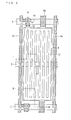
- Fig. 2 is a plane view illustrating one pixel area of an active matrix substrate of the present embodiment.
- An active matrix substrate of the present embodiment includes: a plurality of source wires 8a and a plurality of gate wires (scanning signal lines) 2, a plurality of rectangular-shaped (straight comblike) pixel electrodes 13, common electrodes 9, common electrode wires 8b, auxiliary electrode wires 3, and TFTs (Thin Film Transistor) 18, as illustrated in Fig. 2 .
- the plurality of source wires 8a and the plurality of gate wires 2 orthogonally intersect with each other.
- Each of the plurality of rectangular-shaped pixel electrodes 13 is provided parallel to the source wires (video signal lines) 8a in areas (pixel areas; later described) surrounded by the source wires 8a and the gate wires 2.
- Each of the common electrodes 9 is provided under the pixel electrodes 13.
- the common electrode wires 8b extend in a parallel direction to the source wires 8a from the common electrodes 9.
- Each of the auxiliary common electrode wires 3 are provided parallel to the gate wires 2 between adjacent gate wires 2.
- each of the common electrode wires 3 are provided between respective two adjacent gate wires 2, as illustrated in Fig. 2 .
- sources (source electrode) which form the TFTs 18 and gates (gate electrode) which also form the TFTs 18 are given identical reference numerals as the source wires and the gate wires, respectively.
- the common electrodes 9 are provided in the pixel areas, and the common electrode wires 8b are provided parallel to the source wires 8a so as to connect adjacent ones of the common electrodes 9. Further, the auxiliary common electrode wires 3 that are connected to the common electrodes 9 via contact holes are provided parallel to the gate wires 2.
- the common electrodes 9 and the auxiliary common electrode wires 3 intersect in the pixel areas, and on the common electrodes 9 at these intersections, contact holes 5 are provided (see (a) of Fig. 1 ).
- contact holes 12 are provided on the pixel electrodes 13 so as to connect the pixel electrodes 13 to respective TFTs 18 (see (a) of Fig. 1 ).
- the contact holes 5 are not necessarily provided in all of the pixel areas, and may be provided in pixel areas alternately skipped by one or two pixel areas.
- This method for manufacturing the active matrix substrate uses six masks.
- the auxiliary common electrode wires 3 are not essential in the arrangement. Therefore, in a case where the auxiliary common electrode wires 3 are not provided, a step for forming the contact hole 5 is unnecessary. As a result, the active matrix substrate can be manufactured by use of five masks.
- a film is formed on the insulating substrate 1 by sputtering Ti/Al/Ti or the like in a thickness of approximately 250 nm. Thereafter, by a photolithography method, the gate 2 and the auxiliary common electrode wires 3 are formed spaced apart from each other. In this step 1, a first mask is to be used.
- the gate insulating film (silicon nitride; SiNx) 4, the a-Si layer 6, and the n+-Si layer 7 are formed consecutively in this order having a thickness of approximately 300 nm, 150 nm, and 50 nm, respectively.
- positions corresponding to the gate 2 and the auxiliary common electrode wires 3 are patterned as an island-shape by the photolithography method, as illustrated in (b) of Fig. 3 . Note that a channel section of the TFT 18 is still not formed at this point.
- a second mask is to be used.
- the gate insulating film 4 provided on the auxiliary common electrode wires 3 is etched in a predetermined pattern by the photolithography method as illustrated in (c) of Fig. 3 , so as to form the contact hole 5 and a wires lead-out terminal pad section (not illustrated) of the gate wires 2 and the source wires 8b.
- a third mask is to be used.
- a transparent conductive layer made of ITO is formed as a lower layer having a thickness of approximately 100 nm, and a metal layer made of Mo/Al/MoN or the like is formed as an upper layer having a thickness of approximately 150 nm, consecutively, by sputtering.
- a photoresist 14 is formed as illustrated in (d) of Fig. 3 .
- the photoresist 14 causes, by a halftone exposure method, a remaining amount of photoresist on the film in (i) an area in which the transparent conductive film and the metal layer are both to be removed, (ii) a first area (an area forming the source 8a or the drain 10) in which the transparent conductive film and the metal layer are both to remain, and (ii) a second area (an area forming the common electrode 9) in which the transparent conductive film and the metal layer are both to remain, to be approximately 0 nm, 3000 nm, and 1000 nm, respectively.
- the photoresist 14 that causes a film to remain by an amount of approximately 3000 nm is also formed on an area on which the common electrode wires 8b are to be formed. In this step, a fourth mask is to be used.
- the metal film is etched by a wet etching method by use of a wet etching liquid containing a phosphoric acid - hydrochloric acid - nitric acid type etching liquid. Further, the transparent conductive film is etched by a wet etching method by use of a ferric chloride etchant. This forms the source 8a and the drain 10, as illustrated in (e) of Fig. 3 .
- the source 8a and the drain 10 are formable as a double-layered structure by carrying out this step, having the transparent conductive film (ITO) 19 as a lower layer and the metal layer 21 as an upper layer. Further, the common electrode 9 is simultaneously formed.
- ITO transparent conductive film
- a bottommost layer of the source 8a and the drain 10 is the transparent conductive film (ITO) 19, and that this bottommost layer being the transparent conductive film (ITO) 19 also serves as the common electrode 9.
- the photoresist 14 provided on the area on which the common electrode 9 is formed is removed by a dry etching method utilizing a gas containing O 2 , as illustrated in (f) of Fig. 3 .
- the metal film on the area on which the common electrode 9 is formed is removed by the wet etching method utilizing the phosphoric acid - hydrochloric acid - nitric acid type etching liquid. Thereafter, a channel section including the a-Si layer 6 and the n + -Si layer 7 is formed by the dry etching method utilizing a gas containing SF 6 . This forms, for each pixel, a TFT 18 which serves as a switching element.
- the photoresist on the area on which the source 8a, the common electrode wires 8b, and the drain 10 are formed is removed by the dry etching method utilizing the gas containing O 2 , as illustrated in (h) of Fig. 2 .
- a silicon nitride film is formed in a thickness in a range of approximately 250 nm to 500 nm so as to serve as the interlayer insulating film 11, by the plasma CVD method.
- This interlayer insulating film 11 is then etched in a predetermined pattern by the photolithography method so as to form the contact hole 12 and the wires lead-out terminal pad section (not illustrated) of the gate wires 2 and source wires 8a.
- the transparent conductive film made of ITO is formed by sputtering in a thickness of approximately 100 nm on the interlayer insulating film 11.
- the pixel electrodes 13 are etched in a predetermined pattern (by use of a sixth mask). This concludes the formation of the active matrix substrate illustrated in (a) of Fig. 1 .
- the active matrix substrate of the present embodiment has a wiring structure in which the source/drain electrodes have transparent electrodes as the bottommost layer, and further has the transparent electrodes that are the bottommost layer to serve as a common electrode, as illustrated in (a) of Fig. 1 .
- the common electrodes are provided on the bottommost layer of the source electrodes/wires and the drain electrodes/wires, and not the ITO (common electrode) serving as a bottommost layer of the gate electrodes/wires.
- the ITO is provided parallel to the gate electrode/wires.
- the present embodiment forms the source electrodes/wires 8a and the drain electrodes/wires 10 by use of a transparent conductive film (ITO) 19 and an opaque metal layer 21 provided on the ITO 19 as an upper layer of the ITO 19. This allows leading out of the common electrode wires 8b formed by the ITO 19 parallel to the source wires.
- ITO transparent conductive film
- the ITO is provided on the bottommost layer of the gate electrodes/wires as with a conventional active matrix substrate, a problem occurs that the gate electrodes/wires roughens since an amorphous silicon on a gate insulating film is positioned on an upper side of the ITO. If the gate electrodes/wires roughens, the flatness decreases and the roughness of the TFT channel section increases. This causes a decrease in mobility. In comparison, the present embodiment does not provide the ITO on the bottommost layer of the gate electrodes/wires. Thus, it is possible to avoid the problem of the amorphous silicon to roughen.
- the ITO has an extremely low transition temperature of crystallization in a case where the ITO is provided on the bottommost layer of the gate electrodes/wires as with the conventional active matrix substrate. That is to say, the ITO polysiliconizes from an amorphous state at around a temperature in a range of 150 ° to 200 °.
- the transparent electrodes are compared between a crystallized state and the amorphous state, a large difference is recognized in an etching rate. Therefore, polysiliconization of the transparent electrodes cause a need to etch for a remarkably long period of time. In other words, over-etching is necessarily carried out.
- the gate wires become back tapered (peaked), which causes a problem that the gate insulting film cannot be covered.
- the ITO is not provided on the bottommost layer of the gate electrodes/wires. As a result, it is possible to avoid such problem.
- the ITO is provided as the bottommost layer of the source electrodes/wires and the drain electrodes/wires. Further, it is arranged such that the common electrode wires formed by the ITO be lead out parallel to the source wires.
- the source wires are shorter than the gate wires.
- a number of wires is 768 ⁇ 1024 (D ⁇ W). Therefore, an aspect ratio of the display section is 3 : 4.
- the number of wires is 1080 ⁇ 1920 (D ⁇ W), and the aspect ratio of the display screen is 9 : 16.
- the present embodiment has the auxiliary common electrode wires 3 provided parallel to the gate electrode/wires 2 between adjacent gate electrode/wires 2, in addition to the common electrode wires 8b provided parallel to the source wires/electrode 8a. That is to say, common electrode wires are reticulately provided, by connection of the wires. This thus allows having an arrangement in which resistance is determined just by relation of the aspect ratio, regardless of a size of a display section. As a result, the resistance between two arbitrary points is reduced. In addition, reticulately providing the common electrode wires allows having redundancy in four directions.
- the metal layer 22 is provided as an upper layer of the common electrode 8b in an area corresponding to the intersecting section of the gate electrodes/wires 2 and the common electrode wires 8b.
- the intersecting section has narrow common electrode wires 8b. Therefore, breaking of the wires may readily occur, and a loss due to resistance is great.
- the common electrode wires 8b having the metal layer 22 as the upper layer of the common electrode wires 8b secures connection at the metal layer even if breaking of the wires occur under the metal layer.
- the loss due to the resistance is suppressed by having a low resistant metal layer 22 stacked on the common electrode wires 8b.
- a semiconductor layer including the a-Si layer 6 and the n + -Si layer 7 is provided in the area corresponding to the intersecting section of the gate electrodes/wires 2 and the common electrode wires 8b. Therefore, it is possible to (i) have a reasonable distance between the gate electrodes/wires 2 and the common electrode wires 8b and (ii) reduce a capacitance between the gate electrodes/wires 2 and the common electrode wires 8b, as compared to an arrangement that does not provide the semiconductor layer.
- the common electrode wires 3 are provided mid between two respective adjacent gate electrodes/wires 2, as illustrated in Fig. 2 . This allows providing a reasonable distance between the common electrode wires 3 and the gate electrodes/wires 2. Consequently, it is possible to reduce the possibility of shortage between the common electrode wires 3 and the gate electrodes/wires 2 caused by poor patterning and adhering of dust.
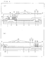
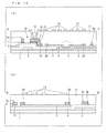
- Fig. 4 illustrates First Modification, wherein (a) is a cross sectional view taken on a line A-A' corresponding to (a) of Fig. 1 , and (b) is a cross sectional view taken on a line B-B' corresponding to (b) of Fig. 1 .
- a plane view of the First Modification is identical to Fig 2 . Therefore, the plane view of the First Modification is omitted here.
- the representative example has a single-layered interlayer insulating film 11 as illustrated in (a) and (b) of Fig. 1 .
- the First Modification has a double-layered interlayer insulating film 11, as illustrated in (a) and (b) of Fig. 4 .
- the interlayer insulating film 11 is so arranged as a double-layered structure including an inorganic film 23 made of SiNx, SiO 2 or the like, and a film 24 made of low-dielectric constant organic material.
- a pinhole or a defect in the single-layered insulting film causes a leakage in the upper and the lower metal layers.
- an echant etching liquid
- the lower metal layer is etched in a case where the single-layered insulating film has the pinhole or defect. This causes breaking of wires and the like.
- the insulating film has some pinhole or defect.
- the First Modification is manufactured by forming, in Step 9, as the interlayer insulating film, an inorganic film made of SiNx, SiO 2 or the like in a thickness in a range of 150 nm to 350 nm, and then forming a film made of low dielectric constant organic material in a thickness in a range of 2000 nm to 4000 nm on the inorganic film.
- the explanation of the First Modification describes an interlayer insulating film of a double-layered structure, however the structure of the interlayer insulating film is not limited to two layers, and may have three or more layers, by arbitrarily stacking the inorganic film 23 made of the SiNx, SiO 2 or the like and the film 24 made of low dielectric constant organic material.
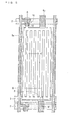
- Fig. 5 illustrates Second Modification, and is a plane view corresponding to Fig. 2 .
- (a) of Fig. 6 is a cross sectional view taken on a line A-A' as indicated in Fig. 5
- (b) of Fig. 6 is a cross sectional view taken on a line B-B' as indicated in Fig. 5 .
- the auxiliary common electrode wires 3 are arranged substantially mid between adjacent gate wires 2, respectively.
- the Second Modification arranges the auxiliary common electrode wires 3 in a vicinity of one of the respective adjacent gate wires 2. More specifically, the auxiliary common electrode wires 3 has a section that does not overlap with the pixel electrodes 13 in an extending direction of the source wires 8a. That is to say, the auxiliary common electrode wires 3 juts out from the pixel electrodes 13 in the extending direction of the source wires 8a.
- the Second Embodiment has a contact hole 5' at least on a part of the common electrode wires 8b.
- the arrangement illustrated in the cross section taken on the line A-A' as indicated in (a) of Fig. 6 that is, the cross section including an area in which the TFT 18 is provided to around a center of the pixel area, does not include the auxiliary common electrode wires 3, as different to Fig. 2(a) .
- the arrangement illustrated in the cross section taken on the line B-B' as indicated in (b) of Fig. 6 that is, the cross section including the area corresponding to the gate wires 2 to the area corresponding to the intersecting section of the gate wires 2 and the common electrode wires 8b via the pixel area includes the auxiliary common electrode wires 3 provided in the pixel area, as different to Fig. 2(b) .
- the auxiliary common electrode wires 3 and the common electrodes 9 are connected via the contact hole 5' formed on a position in which a part overlaps with the area of the common electrode wires 8b.
- the disabled area denotes areas of the following (A) through (D):
- the disabled area is (A) + (B) + (C) + (D).
- the disabled area is the area excluding the overlapping portions of the disabled areas (B) and (C) with area (A).
- the disabled area is reduced in the Second Modification as compared to the representative example. This allows realization of the high aperture ratio.
- the Second Modification is manufactured by changing, in Step 1, a provided position of the auxiliary common electrode wires 3 to a position closer to the gates 2.
- auxiliary common electrode wires 3 in the representative example is simply one example, and may be in any position as long as the auxiliary common electrode wires 3 are positioned between two adjacent gate wires 2.
- Fig. 7 illustrates Third Modification, and is a plane view corresponding to Fig. 2 .
- (a) of Fig. 8 is a cross sectional view taken on a line A-A' as indicated in Fig. 7
- (b) of Fig. 8 is a cross sectional view taken on a line B-B' as indicated in Fig. 7 .
- the Third Modification in addition to the arrangement of the representative example, has the auxiliary common electrode wires 3 extend to an outer peripheral section (disabled area) of the pixel area, and extend in the outer peripheral section so as to be parallel to the source wires 8a, as illustrated in Fig. 7 .
- the auxiliary common electrode wires 3 are extended to a surrounding section (outer peripheral section) of the common electrodes 9, and extended in the surrounding section so as to be parallel to the source wires 8a.
- a shape of the auxiliary common electrode wires 3 from a plane view is in an H-shape.
- the cross section of (a) of Fig. 8 taken on the line A-A' does not pass through characteristic parts of the Third Modification, therefore is identical to (a) of Fig. 2 .
- the auxiliary common electrode wires 3 is provided on the insulating substrate 1 in the disabled area (area in which liquid crystal does not move, and liquid crystal domain occurrence area) on the source wires 8a side of the pixel areas. Therefore, light shielding of the disabled area is possible without the need to add any processes to the representative example. This allows attainment of a high display quality.
- the Third Modification is manufactured by forming, in Step 1, the auxiliary common electrode wires 3 parallel to the source wires 8a in the disabled area on the source wires 8a side of the pixel areas.
- auxiliary common electrode wires 3 may be provided so as to extend to the outer peripheral section of the pixel area, and extend in the outer peripheral section so as to be parallel to the source wires 8a, and also extend in the outer peripheral section so as to be parallel to the gate wires 2, so as to surround the entire outer peripheral section of the pixel areas. That is to say, the common electrode wires 3 may be provided in a ring shape.
- Fig. 9 illustrates Fourth Modification, and is a plane view corresponding to Fig. 2 .
- (a) of Fig. 10 is a cross sectional view taken on a line A-A' as indicated in Fig. 9
- (b) of Fig. 10 is a cross sectional view taken on a line B-B' as indicated in Fig. 9 .
- a same metal layer as the metal layer 21 which is provided as the upper layer of the source 8a and the drain 10 is provided as a light shielding film (metal layer provided so as to surround outer peripheries of the common electrodes) 25 so as to shield a liquid crystal domain, at a surrounding section (outer peripheral section) of the common electrodes 9, as illustrated in Fig. 9 , and (a) and (b) of Fig. 10 .
- the light shielding film 25 may be provided so as to cover the entire common electrode wires 8b, as illustrated in Fig 9 .
- the metal layer used for the light shielding film 25 is not limited to ones that have a function of a light shielding film. Namely, the light shielding function is simply one example.
- the light shielding film 25 is formed by not removing all of a metal film corresponding to a position on which the common electrodes 9 are to be formed but have the metal film remain on the surrounding section of the common electrodes 9, when removing the metal film in Step 7.
- the arrangement allows surroundings of the common electrodes 9 to have a light shielding function, and allows reduction of a resistance of the common electrodes 9 and the auxiliary common electrode wires 3, by providing the light shielding film 25 that is made of a low resistance metal layer.
- Fig. 11 illustrates Fifth Modification, and is a plane view corresponding to Fig. 2 .
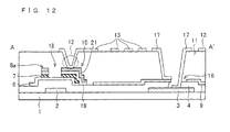
- Fig. 12 is a cross sectional view taken on a line A-A' as indicated in Fig. 11 .
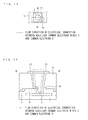
- Fig. 13 is an enlarged view of section C illustrated in Fig. 11 , that is, an intersecting section of the common electrode 9 and the common electrode wires 3.
- Fig. 14 is a cross sectional view taken on a line B-B' as indicated in Fig. 13 .
- the pixel electrodes 13 illustrated in the Fifth Modification are cut off at a part in which the common electrodes 9 and the auxiliary common electrode wires 3 intersect with each other.
- contact electrode pads 17 are provided separated from the pixel electrodes 13. The contact electrode pads 17 electrically connect the common electrodes 9 and the auxiliary common electrode wires 3.
- Reference numeral 16 in Fig. 13 illustrates an opening of the common electrodes 9. That is to say, in the Fifth Modification, an opening is provided at the intersecting section of the common electrodes 9 and the auxiliary common electrode wires 3, as illustrated in Figs. 12 and 14 . Further, as obvious from Figs. 12 and 14 , the interlayer insulating film 11 and the gate insulating film 4 are hollowed out at a position in which the contact electrode pad 17 is provided.
- the common electrodes 9 and the auxiliary electrode wires 3 are electrically connected to each other via the contact holes 5 provided on the gate insulating film 4.
- the Fifth Modification provides the contact electrode pads 17 that are connected to both the common electrodes 9 and the auxiliary common electrode wires 3, as illustrated in Figs. 12 and 14 .
- the common electrodes 9 and the auxiliary common electrode wires 3 are connected to each other via the contact electrode pads 17.
- the contact electrode pads 17 are formed along the interlayer insulating film 11, and one end is connected to the common electrodes 9, and the other end is connected to the auxiliary common electrode wires 3. This allows electrical connection between the auxiliary common electrode wires 3 and the common electrodes 9 as indicated by the broken arrow in Fig. 14 .
- the contact electrode pad 17 can be simultaneously formed with the formation of the pixel electrodes 13. Note that, although the contact electrode pads 17 connect the common electrodes 9 and the auxiliary common electrode wires 3 in the extending direction of the source wires 8a, this is simply one example, and the common electrodes 9 and the auxiliary common electrode wires 3 may be connected in an extending direction of the gate wires 2, for example.
- the Fifth Modification can manufacture the active matrix substrate in a five-mask process.
- a reason of this is because the contact holes 5 can be formed simultaneously with a photopatterning of the interlayer insulating film 11. This enables elimination of a photo step for forming the contact holes 5.
- a film is formed on the insulating substrate 1 by sputtering Ti/Al/Ti or the like in a thickness of approximately 250 nm. Thereafter, by a photolithography method, the gates 2 and the auxiliary common electrode wires 3 are formed spaced apart from each other. In this step 1, a first mask is to be used.
- the gate insulating film (silicon nitride; SiNx) 4, the a-Si layer 6, and the n+-Si layer 7 are formed consecutively in this order having a thickness of approximately 300 nm, 150 nm, and 50 nm, respectively.
- positions corresponding to the gates 2 and the auxiliary common electrode wires 3 are patterned as an island-shape by the photolithography method, as illustrated in (b) of Fig. 15 . Note that a channel section of the TFTs 18 is still not formed at this point.
- a second mask is to be used.
- a transparent conductive layer made of ITO is formed as a lower layer having a thickness of approximately 100 nm, and a metal layer made of Mo/Al/MoN or the like is formed as an upper layer having a thickness of approximately 150 nm, consecutively, by sputtering.
- a photoresist 14 is formed as illustrated in (c) of Fig. 15 .
- the photoresist 14 causes, by a halftone exposure method, a remaining amount of photoresist on the film in (i) an area in which the transparent conductive film and the metal layer are both to be removed, (ii) a first area (an area forming the sources 8a or the drains 10) in which the transparent conductive film and the metal layer are both to remain, and (ii) a second area (an area forming the common electrodes 9) in which the transparent conductive film and the metal layer are both to remain, to be approximately 0 nm, 3000 nm, and 1000 nm, respectively.
- the photoresist 14 that causes a film to remain by an amount of approximately 3000 nm is also formed on an area on which the common electrode wires 8b are to be formed.
- a third mask is to be used.
- the metal film is etched by a wet etching method by use of a wet etching liquid containing a phosphoric acid - hydrochloric acid - nitric acid type etching liquid. Further, the transparent conductive film is etched by a wet etching method by use of a ferric chloride etchant. This forms the sources 8a and the drains 10, as illustrated in (d) of Fig. 15 .
- the sources 8a and the drains 10 are formable as a double-layered structure by carrying out this step, having the transparent conductive film (ITO) 19 as a lower layer and the metal layer 21 as an upper layer. Further, the common electrodes 9 are simultaneously formed.
- ITO transparent conductive film
- the photoresist 14 provided on the area on which the common electrodes 9 are formed is removed by a dry etching method utilizing a gas containing O 2 , as illustrated in (e) of Fig. 15 .
- the metal film on the area on which the common electrodes 9 are formed is removed by the wet etching method utilizing the phosphoric acid - hydrochloric acid - nitric acid type etching liquid. Thereafter, channel sections including the a-Si layer 6 and the n + -Si layer 7 are formed by the dry etching method utilizing a gas containing SF 6 . This forms, for each pixel, TFTs 18 which serve as a switching element.
- the photoresist on the area on which the sources 8a, the common electrode wires 8b, and the drains 10 are formed is removed by the dry etching method utilizing the gas containing O 2 , as illustrated in (g) of Fig. 15 . Note that, although not illustrated in the drawing, the photoresist on the area on which the common electrode wires 8b are formed is simultaneously removed.
- a silicon nitride film is formed in a thickness in a range of approximately 150 nm to 650 nm so as to serve as the interlayer insulating film 11, by the plasma CVD method, as illustrated in (h) of Fig. 15 .
- This interlayer insulating film 11 is then etched in a predetermined pattern by the photolithography method so as to form the contact holes 5 and 12, and the wires lead-out terminal pad section (not illustrated) of the gate wires 2 and source wires 8a.
- dry etching of the gate insulating film 4 is carried out by use of the interlayer insulating film 11 as a mask, so that the contact holes 5 are hollowed to reach the auxiliary common electrode wires 3.
- the transparent conductive film made of ITO is formed by sputtering in a thickness of approximately 100 nm on the interlayer insulating film 11, as illustrated in (i) of Fig. 15 . Thereafter, the pixel electrodes 13, and the contact electrode pads 17 that electrically connect the common electrodes 9 and the auxiliary common electrode wires 3, are etched in a predetermined pattern by the photolithography method. This concludes the formation of the active matrix substrate as illustrated in Fig. 12 . In this step, a fifth mask is to be used.
- the Fifth Modification can manufacture the active matrix substrate by use of five masks.
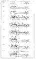
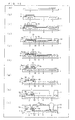
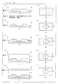
- FIG. 16 (a) through (e) are cross sectional views illustrating a manufacturing process of the contact hole 5 part of the active matrix substrate in a case where six masks are used, and (f) through (j) are schematic views illustrating plane views of Figs. (a) through (e), respectively.
- a first mask is used so as to form the auxiliary common electrode wires 3, as illustrated in (a) of Fig. 16 .
- a second mask is used in a photolithography method of a semiconductor layer (not illustrated).
- a third mask is used so as to form the contact holes 5, as illustrated in (b) of Fig. 16 .
- a fourth mask is used so as to form the common electrodes 9, as illustrated in (c) of Fig. 16 .
- a fifth mask is used so as to pattern the interlayer insulating film 11, as illustrated in (d) of Fig. 16 .
- a sixth mask is used so as to form the pixel electrodes 13, as illustrated in (e) of Fig. 16 .
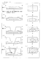
- FIG. 17 are cross sectional views illustrating a manufacturing process of the contact hole 5 part of the active matrix substrate in a case where five masks are used, and (f) through (j) are schematic views illustrating plane views of (a) through (e), respectively.
- a first mask is used so as to form the auxiliary common electrode wires 3 as illustrated in (a) of Fig. 17 .
- a second mask is used in a photolithography method of a semiconductor layer (not illustrated).
- a third mask is used so as to form openings 16 of the common electrodes 9, as illustrated in (b) of Fig. 17 .
- a fourth mask is used so as to form the interlayer insulating film 11 as illustrated in (c) of Fig. 17 .
- Formation of the contact holes 5 that extend to the auxiliary common electrode wires 3 are carried out by dry etching the gate insulating film 2 by use of the interlayer insulating film 11 as a mask. Therefore, a new mask is not necessary in (d) of Fig. 17 .
- a fifth mask is used so as to form (i) the pixel electrodes 13 and (ii) the contact electrode pads 17 that electrically connect the common electrodes with the auxiliary common electrode wires 3, as illustrated in (e) of Fig. 17 .
- the arrow illustrated in broken lines in (d) of Fig. 17 indicates a flowing direction of an electrical connection between the auxiliary common electrode wires 3 and the common electrodes 9.
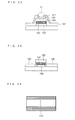
- FIG. 18 A comparative example is illustrated in (a) and (b) of Fig. 18 , whose openings 16 of common electrodes 9 are larger than openings of contact holes 5.
- (a) of Fig. 18 is a plane view
- (b) of Fig. 18 is a cross sectional view taken on a line B-B' as indicated in (a) of Fig. 18 .
- the contact electrode pads 17 are electrically connected to the auxiliary common electrode wires 3, however cannot be electrically connected to the common electrodes 9. The reason of this is obvious; therefore it is omitted here.
- FIG. 19 Another comparative example is illustrated in (a) and (b) of Fig. 19 , whose openings 16 of common electrodes 9 are smaller that of openings of contact holes.
- (a) of Fig. 19 is a plane view
- (b) of Fig. 19 is a cross sectional view taken on a line B-B' as indicated in (a) of Fig. 19 .
- the contact electrode pads 17 are electrically connected to the common electrodes 9, however cannot be electrically connected to the auxiliary common electrode wires 3.
- the common electrodes 9 are made of material such as ITO, the common electrodes 9 cannot be dry etched when the contact holes 5 are hollowed to the auxiliary common electrode wires 3 by dry etching the gate insulating film 4 by use of the interlayer insulating film 11 as a mask.
- the gate insulating film 4 becomes back tapered, in other words, peaked, which causes the contact electrode pads 17 to be disconnected.
- the active matrix substrate in the Fifth Modification of the present embodiment is so arranged that the contact electrode pads 17 are electrically connectable to both the common electrodes 9 and the auxiliary common electrode wires 3. That is to say, the Fifth Modification is so arranged that both arrangements of the two comparative examples are taken into account. Furthermore, in other words, the contact electrode pads 17 are connected to (i) the auxiliary common electrode wires 3 on a first end sections side of the common electrodes 9 located outside of an outer edge of the respective one of the contact holes 5, and (ii) the common electrodes on a second end sections side of the common electrodes 9 located inside of the outer edge of the respective one of the contact holes 5.
- the regular six mask process requires, before the formation of the sources and the drains, adding of a photo step so as to form the contact holes 5 that electrically connect the common electrodes 9 with the auxiliary common electrode wires 3.
- the photo step for forming the contact holes 5 is not carried out before the formation of the sources and the drains. Instead, openings are provided on parts of the common electrodes 9 (so as to allow hollowing out of the contact holes 5 to the bottommost layer of the auxiliary common electrode wires 3 later on). This allows the formation of the contact holes 5 simultaneously with the photopatterning of the interlayer insulating film 11.
- the contact electrode pads 17 that electrically connect the common electrodes 9 with the auxiliary common electrode wires 3 are formed at the time when the pixel electrodes 13 are formed.
- This enables the manufacture of the active matrix substrate by use of the five masks.
- the arrangement described in claim 1 does not require the foregoing processes, and is of a five-mask process. This is because the photopatterning step of the contact holes 5 carried out before the formation of the sources and the drains is originally not included.
- the pixel electrodes are of a straight comblike shape.
- Sixth Modification adds a change in a shape of the pixel electrodes 13.
- the pixel electrodes 13 may be of a V-shape whose center is positioned mid between two adjacent ones of the source wires 8a in the pixel areas, as illustrated in (a) of Fig. 20 .
- the pixel electrode 13 may be of a V-shape whose center is positioned mid between two adjacent ones of the gate wires 2 in the pixel areas.
- the present modification has the metal layer 21 which is the upper layer of the sources 8a remaining on the common electrodes 9 in areas in which a liquid crystal domain may occur. That is to say, as illustrated in (a) and (b) of Fig. 20 , the metal layer 21 is provided on parts of the common electrodes 9 (broken line section in (a) and (b) of Fig. 20 ).
- Having the pixel electrodes 13 in such a shape allows realization of a multi-domain broad angle of view.
- an active matrix substrate includes an insulating substrate; video signal lines and scanning signal lines provided orthogonally intersecting with each other on the insulating substrate; and thin film transistors provided at intersections of the video signal lines and the scanning signal lines, the thin film transistors including gate electrodes, source electrodes, and drain electrodes, respectively, a transparent electrode layer, formed to be used as a lower layer of the source electrodes and the drain electrodes, being used as (i) common electrodes provided in pixel areas surrounded by adjacent video signal lines and adjacent scanning signal lines, respectively and (ii) common electrode wires for connecting adjacent ones of the common electrodes parallel to the video signal lines.
- the invention is applicable to a liquid crystal display device, and is particularly suitable for use in large-screen televisions and the like.
Landscapes
- Physics & Mathematics (AREA)
- Nonlinear Science (AREA)
- Mathematical Physics (AREA)
- Chemical & Material Sciences (AREA)
- Crystallography & Structural Chemistry (AREA)
- General Physics & Mathematics (AREA)
- Optics & Photonics (AREA)
- Engineering & Computer Science (AREA)
- Microelectronics & Electronic Packaging (AREA)
- Geometry (AREA)
- Liquid Crystal (AREA)
- Thin Film Transistor (AREA)
Abstract
Description
- The present invention relates to an active matrix substrate which incorporates a TFT, and a liquid crystal display device including the active matrix substrate.
- There has been known of liquid crystal display devices of an FFS (Fringe Field Switching) mode. A liquid crystal display device of the FFS mode is arranged such that a counter electrode and a pixel electrode (i) are formed by transparent material such as ITO, (ii) have a narrower space between the counter electrode and the pixel electrode than a space between the upper and lower substrates, and further (iii) have a width between the counter electrode and the pixel electrode in a degree in which all of liquid molecules aligned on an upper part of an electrode are drivable.
- The liquid crystal display device of the FFS mode can attain a higher aperture ratio than that of a liquid crystal display device of an IPS (In-Place-Switching) mode, since the electrodes and the like are formed by the transparent material. That is to say, a higher aperture ratio than that of the IPS mode is attainable by causing light transmission to occur at an electrode section.
- In
Fig. 21 , (a) is a plane view of an active matrix substrate to be used in a liquid crystal display device of the FFS mode, as described inPatent Document 1, and (b) is a cross sectional view taken on line A-A' indicated in (a) ofFig. 21 . - As illustrated in (a) of
Fig. 21 , the active matrix substrate mainly includes: a plurality ofgate bus lines 101 and a plurality ofsource bus lines 107 which orthogonally intersect with each other; a plurality ofpixel electrodes 109 provided comblike and parallel to thesource bus lines 107 in pixel areas surrounded by the gate and source bus lines, respectively;TFTs 103 provided on sections in which thegate bus lines 101 diverge to the pixel area side; and common electrode wires (CS wires) 110 provided parallel to thegate bus lines 101. - Further, as illustrated in (b) of
Fig. 21 , the active matrix substrate has common electrodes (gate bus line lower layer) 106 which consist of a transparent conductive film on an insulating substrate. Further, on thecommon electrodes 106 are provided a gate bus lineupper layer 101 andCS wires 110. Moreover, asemiconductor layer 103, acontact layer 104, and a source/drain electrodeupper layer 107 are stacked on the gate bus lineupper layer 101 sandwiching agate insulating film 102 between thesemiconductor layer 103 and the gate bus lineupper layer 101, so as to form a TFT. On an uppermost layer of the active matrix substrate is providedpixel electrodes 109 via an interlayer insulating film (passivation film) 108. - The active matrix substrate described in
Patent Document 1 has the following two problems, caused by the common electrodes which form theCS wires 110 being provided on the gate bus linelower layer 106. - Namely, as illustrated in
Fig. 22 , roughening of the common electrodes and the gate bus line upper layer causes thesemiconductor layer 103, thecontact layer 104, and the source/drain electrodeupper layer 107 that are provided on thegate insulating film 102 to also roughen. Note that thesemiconductor layer 103, thecontact layer 104, and the source/drain electrodeupper layer 107 form achannel section 111 of the TFT. Particularly, in a case where a common transparent metal film is used as transparent electrodes, the flatness becomes low. This causes the roughness of thechannel section 111 of the TFT to increase. As a result, a problem of a decrease in mobility occurs. - Moreover, the transparent electrodes have an extremely low transition temperature of crystallization, that is, the transparent electrodes polysiliconize (crystallize) from an amorphous state at around a temperature in a range of 150 ° to 200 °. When the transparent electrodes are compared between a crystallized state and the amorphous state, a large difference is recognized in an etching rate. Therefore, polysiliconization of the transparent electrodes causes a need to etch for a remarkably long period of time. Namely, as illustrated in
Fig. 23 , over-etching is required. As a result, thegate bus lines 101 become back tapered (peaked), and thegate insulating film 102 cannot cover thegate bus lines 101. This causes a problem that an efficiency percentage decreases, such as occurrence of leaking from the metal thin film formed on the upper layer. - An active matrix substrate described in
Patent Document 2 provides common electrodes on a gate insulating film. In other words, the common electrodes are provided on a layer upper than the gate bus lines. Therefore, the two aforementioned problems are solved. - However,
Patent Documents CS wires 123 are horizontally provided, as illustrated inFig. 24 . Generally, in liquid crystal display devices, many liquid crystal display sections are wide-shaped. Therefore, the gate bus lines are longer as compared to the source bus lines. Consequently, the common electrodes formed at theCS wires 123 have a high resistance, which causes a problem of signal delay. However in order to solve this problem, if a width of theCS wires 123 is thickened so as to aim for low resistance, another problem occurs that an aperture ratio decreases. - In response to this,
Patent Document 3 provides the common electrodes (transparent electrode material, for example ITO) on a further upper position than the pixel electrodes, as illustrated inFig. 25 . The transparent electrode material is left remaining on all of an area except for a slit section of the common electrodes, so as to form the common electrodes. Further, as illustrated inFig. 26 , the transparent electrode material (CS wires) is provided on substantially the entire source bus lines and gate bus lines. As such, the problem of signal delay is solved by providing the CS wires parallel to the source bus lines. - [Patent Document 1]
Japanese Unexamined Patent Publication No.235763/2001 2001-235763; published on August 31, 2001 - [Patent Document 2]
Japanese Unexamined Patent Publication No.90781/2002 2002-90781; published on March 27, 2002 - [Patent Document 3]
International Patent Publication No.WO 01/18597 (published on March 15, 2001 - [Patent Document 4]
Japanese Unexamined Patent Publication No.221992/2001 2001-221992; published on August 17, 2001 - [Patent Document 5]
Japanese Unexamined Patent Publication No.230380/1997 9-230380; published on September 5, 1997 - However, in the technique disclosed in
Patent Document 3, the CS wires are formed so as to cover the entire source bus lines and gate bus lines illustrated inFig. 26 . Therefore, defects such as a shortage and the like may possibly occur, and a parasitic capacitance between the gate and source bus lines and the CS wires increases. - The present invention is attained in view of the problems, and its purpose is to provide an active matrix substrate and a liquid crystal display device including the same that has small signal delay caused by resistance and small signal delay caused by parasitic capacitance.
- In order to attain the above object, an active matrix substrate of the present invention includes an insulating substrate; video signal lines and scanning signal lines provided orthogonally intersecting with each other on the insulating substrate; and thin film transistors provided at intersections of the video signal lines and the scanning signal lines, the thin film transistors including gate electrodes, source electrodes, and drain electrodes, respectively, a transparent electrode layer, formed to be used as a lower layer of the source electrodes and the drain electrodes, being used as (i) common electrodes provided in pixel areas surrounded by adjacent video signal lines and adjacent scanning signal lines, respectively and (ii) common electrode wires for connecting adjacent ones of the common electrodes parallel to the video signal lines.
- According to the arrangement, a transparent electrode layer that is formed to be used as a lower layer of source electrodes and drain electrodes is used as (i) common electrodes provided in pixel areas surrounded by adjacent video signal lines and adjacent scanning signal lines, respectively and (ii) common electrode wires for connecting adjacent ones of the common electrodes parallel to the video signal lines. In other words, the common electrodes and the common electrode wires are formed by use of the transparent electrode layer that is to be used as a lower layer of the source electrodes and the drain electrodes. This allows the common electrodes to be connected and extended in a parallel direction to the video signal lines that are connected to the source electrodes. Generally, video signal lines are shorter than the scanning signal lines. Therefore, it is possible to reduce resistance as compared to the common electrodes being extended parallel to the scanning signal lines.
- Furthermore, according to the arrangement, the common electrode wires do not have any part overlapping with the video signal lines, and are formed so as to overlap at a part where the common electrode wires orthogonally intersect with the scanning signal lines. When focused on one common electrode that is formed between adjacent video signal lines, generally a number of video signal lines is more than that of the scanning signal lines (video signal lines : scanning signal lines = 3(RGB) :
- 1). Therefore, a number of overlapping parts of the common electrodes and each signal lines (video signal lines, scanning signal lines) is reduced as compared to a conventional arrangement in which the common electrodes overlap at the parts orthogonally intersecting with the video signal lines. As a result, the parasitic capacitance of the common electrode wires is reduced.
- As described above, the present invention reduces the resistance of the common electrodes and the common electrode wires, as well as reducing the parasitic capacitance between the common electrode wires and the signal lines. Therefore, it is possible to reduce the signal delay of the common electrode wires.
- Further, according to the arrangement, a transparent electrode layer (transparent conductive material such as ITO) is formed as a lower layer of the source electrodes and the drain electrodes. This allows formation of the common electrodes in a same photolithography step as the formation of the source electrodes and the drain electrodes by use of a photolithography step that utilizes so-called halftone exposure. As a result, simplification of a manufacturing method is possible. In addition, since the common electrodes are formable in the same photolithography step, a decrease in yield rate caused by the photo alignment disposition and decrease in aperture ratio are prevented as compared to formation of the source and drain electrodes in a different photo step to the common electrodes, as in
Patent Document 2 described above. - The active matrix substrate of the present invention is preferably arranged such that a metal film formed so as to create the gate electrodes is used as auxiliary common electrode wires that are provided parallel to the scanning signal lines, and the auxiliary common electrode wires and the common electrodes are electrically connected to each other via contact holes, respectively.
- According to the arrangement, auxiliary common electrode wires are provided parallel to the scanning signal lines, and the auxiliary common electrode wires and the common electrodes are electrically connected to each other via contact holes, respectively, provided on the gate insulating film. That is to say, a reticulate structure is formed by use of the common electrodes, common electrode wires and the auxiliary common electrode wires. Therefore, it is possible to have the structure close to one which a resistance is determined just by a relation of an aspect ratio (concept of sheet resistance), regardless of its size and material. Therefore, it is possible to reduce the resistance between two arbitrary points. Further, in the technique described in
Patent Document 2, thecommon electrodes 120 and thecommon electrode wires 121 are connected to each other via source metals (metal layer of source bus lines) as illustrated inFig. 27 . This causes a problem of pixel defect in a case where ohmic contact cannot be made. However, the reticulate structure enables the common electrodes to have four-directional redundancy. Therefore, even if a pixel that cannot make the ohmic contact, or, further even if one of the common electrodes and/or the auxiliary common electrodes have a breakage, the pixel defect and line defect is prevented to the utmost. - The active matrix substrate of the present invention is preferably arranged such that each of the common electrodes has an opening section whose first and second end sections are located outside and inside, respectively, of an outer edge of a respective one of the contact holes; and contact electrode pads connected to (i) the auxiliary common electrode wires on the first end sections side of the common electrodes, and (ii) the common electrodes on the second end sections side of the common electrodes, respectively.
- According to the arrangement, each of the common electrodes has an opening whose first and second end sections are located outside and inside, respectively, of an outer edge of a respective one of the contact holes, and contact electrode pads are connected to (i) the auxiliary common electrode wires on the first end sections side of the common electrodes, and (ii) the common electrodes on the second end sections side of the common electrodes, respectively. This allows electrical connection between the common electrodes and the auxiliary common electrode wires by use of the contact electrode pads. Moreover, this allows elimination of a contact hole forming step for connecting the common electrodes and the auxiliary common electrode wires, which forming step is to be carried out before formation of the source wires/electrodes and the drain electrodes.
- The active matrix substrate of the present invention is preferably arranged such that the pixel areas include pixel electrodes, and the contact electrode pads are formed to be made of a same material and in a same manufacturing step as the pixel electrodes.
- According to the arrangement, pixel electrodes and contact pads are formed by a same material and in a same manufacturing step. This allows simplification of a manufacturing method.
- The active matrix substrate of the present invention is preferably arranged such that the auxiliary common electrode wires are provided substantially mid between adjacent ones of the scanning signal lines, respectively.
- According to the arrangement, the auxiliary common electrode wires are provided substantially mid between adjacent ones of the scanning signal lines. The auxiliary common electrode wires are provided parallel to the scanning signal lines. Therefore, by providing the auxiliary common electrode wires substantially mid between the adjacent ones of the scanning signal lines, a distance between the auxiliary common electrode wires and the scanning signal lines is maximized. A longer distance from the auxiliary common electrode wires to the scanning signal line reduces a possibility of a shortage in the auxiliary common electrode wires and the scanning signal lines due to poor patterns and adherence of dust.
- The active matrix substrate of the present invention is preferably arranged such that the auxiliary common electrode wires are provided in a vicinity of one of adjacent ones of the scanning signal lines.
- According to the arrangement, the auxiliary common electrode wires are provided in a vicinity of one of the adjacent ones of the scanning signal lines. In the vicinity of the scanning signal lines is an area that does not contribute to an aperture. Therefore, it is possible to realize a high aperture ratio since parts of the auxiliary common electrode wires are provided on the area which does not contribute to the aperture.
- The active matrix substrate of the present invention is preferably arranged such that the auxiliary common electrode wires extend to outer peripheral sections of the common electrodes, and extend in the outer peripheral sections so as to be parallel to the video signal lines, respectively.
- The outer peripheral section of the common electrode has a so-called disabled area (an area in which liquid crystal does not move, and a liquid crystal domain occurrence area). According to the present invention, the auxiliary common electrode wires extend to the outer peripheral section of the common electrodes and extend in the outer peripheral sections so as to be parallel to the video signal lines, respectively. Therefore, light shielding of the disabled area is carried out by the auxiliary common electrode wires, therefore allows attainment of a high display quality.
- The active matrix substrate of the present invention is preferably arranged such that the auxiliary common electrode wires also extend to the outer peripheral sections of the common electrodes, and extend in the outer peripheral sections so as to be parallel to the scanning signal lines, respectively.
- According to the arrangement, it is possible to reduce resistance of the auxiliary common electrode wires and shield light from the disabled area of the scanning signal lines.
- The active matrix substrate of the present invention is preferably arranged such that a metal layer is provided so as to surround outer peripheries of the common electrodes, the metal layer being stacked to be used as an upper layer of the source electrodes and the drain electrodes.
- According to the arrangement, a metal layer stacked to be used as an upper layer of the source electrodes and the drain electrodes is provided so as to surround outer peripheries of the common electrodes. This allows the outer peripheries of the common electrodes to have a light shielding function, and the resistance between the common electrodes and the auxiliary common electrode wires is reduced.
- The active matrix substrate of the present invention is preferably arranged such that the metal layer is formed on parts on which the common electrode wires are provided.
- In addition, the active matrix substrate of the present invention is preferably arranged such that a metal layer is provided on intersections of the common electrode wires and the scanning signal lines.
- According to the arrangement, a metal layer is provided on intersections of the common electrode wires and the scanning signal lines. Therefore, it is possible to reduce the resistance of the common electrode wires. Further, the common electrode wires are of a stacked structure having the transparent electrode layer and the metal layer. This enables reduction of malfunction in the intersecting section with the scanning signal line such as breakage.
- The active matrix substrate of the present invention further preferably includes an interlayer insulating film including at least two layers, the two layers being a layer composed of an inorganic film and a layer composed of a low dielectric constant organic material.
- Here, low dielectric constant organic material denotes for example material having a dielectric constant of not more than 5. According to the arrangement, an interlayer insulating film includes at least two layers, a layer composed of inorganic film and a layer composed of low dielectric constant organic material. Providing the low dielectric constant organic material allows decreasing of the parasitic capacitance. Further, by arranging the interlayer insulating film as having at least two layers, defects such as leakage is reduced. As a result, high reliability is realized.
- A liquid crystal display device of the present invention preferably includes any one of the foregoing active matrix substrates.
- For a fuller understanding of the nature and advantages of the invention, reference should be made to the ensuing detailed description taken in conjunction with the accompanying drawings.
-
-
Fig. 1 is a cross sectional view illustrating one pixel area of an active matrix substrate of an embodiment in the present invention, wherein (a) is a cross sectional view taken on a line A-A' as indicated inFig. 2 , and (b) is a cross sectional view taken on a line B-B' as indicated inFig. 2 . -
Fig. 2 is a plane view illustrating one pixel area in an active matrix substrate of the present embodiment. -
Fig. 3 is a cross sectional view illustrating a manufacturing process of the active matrix substrate of an embodiment in the present invention, wherein (a) through (i) are cross sectional views illustrating a manufacturing process of the active matrix substrate illustrated in (a) ofFig. 1 . -
Fig. 4 is a cross sectional view illustrating a first modification of the embodiment, wherein (a) is a cross sectional view corresponding to the line A-A' in (a) ofFig. 1 , and (b) is a cross sectional view corresponding to the line B-B' in (b) ofFig. 1 . -
Fig. 5 illustrates an embodiment of the present invention, and is a plane view of a second modification, corresponding toFig. 2 . -
Fig. 6 is a cross sectional view illustrating the second modification of the embodiment in the present invention, wherein (a) is a cross sectional view taken on a line A-A' as indicated inFig. 5 , and (b) is a cross sectional view taken on a line B-B' as indicated inFig. 5 . -
Fig. 7 illustrates an embodiment of the present invention, and illustrates a plane view of a third modification, corresponding toFig. 2 . -
Fig. 8 is a cross sectional view illustrating a third modification of the embodiment in the present invention, wherein (a) is a cross sectional view taken on a line A-A' as indicated inFig. 7 , and (b) is a cross sectional view taken on a line B-B' as indicated inFig. 7 . -
Fig. 9 illustrates an embodiment of the present invention, and is a plane view of a fourth modification, corresponding toFig. 2 . -
Fig. 10 is a cross sectional view illustrating the fourth modification of the embodiment in the present invention, wherein (a) is a cross sectional view taken on a line A-A' as indicated inFig. 9 , and (b) is a cross sectional view taken on a line B-B' as indicated inFig. 9 . -
Fig. 11 illustrates an embodiment of the present invention, and is a plane view of a fifth modification, corresponding toFig. 2 . -
Fig. 12 illustrates an embodiment of the present invention, and is a cross sectional view taken on a line A-A' as indicated inFig. 11 . -
Fig. 13 illustrates an embodiment of the present invention, and is an enlarged view of a section C illustrated inFig. 3 , that is, an intersecting section of a common electrode and auxiliary common electrode wires. -
Fig. 14 illustrates an embodiment of the present invention, and is a cross sectional view taken on a line B-B' as indicated inFig. 13 . -
Fig. 15 is a cross sectional view illustrating a manufacturing process of an active matrix substrate of an embodiment in the present invention, wherein (a) through (i) illustrates cross sectional views of a manufacturing process of the active matrix substrate illustrated inFig. 12 . -
Fig. 16 illustrates an embodiment of the present invention, and is a cross sectional view and a plane view illustrating a formation method of a contact section in a six-mask process, wherein (a) through (e) are cross sectional views, and (f) through (j) are plane views. -
Fig. 17 illustrates an embodiment of the present invention, and is a cross sectional view and a plane view illustrating a formation method of a contact section in a five-mask process, wherein (a) through (e) are cross sectional views, and (f) through (j) are plane views. -
Fig. 18 is a plane view and a cross sectional view of a comparative example ofFigs. 13 and 14 that illustrate an embodiment of the present invention, wherein (a) is a plane view, and (b) is a cross sectional view. -
Fig. 19 is a plane view and a cross sectional view of a comparative example ofFigs. 13 and 14 that illustrate an embodiment of the present invention, wherein (a) is a plane view, and (b) is a cross sectional view. -
Fig. 20 is a plane view of a sixth modification of the embodiment in the present invention, wherein (a) and (b) are plane views illustrating the sixth modification, corresponding toFig. 2 . -
Fig. 21 is a plane view and a cross sectional view of an active matrix substrate used in a conventional liquid crystal display device of an FFS mode, wherein (a) is a plane view of the active matrix substrate used in the conventional liquid crystal display device of the FFS mode, and (b) is a cross sectional view taken on a line A-A' as indicated in (a). -
Fig. 22 is a cross sectional view of an active matrix substrate illustrating a conventional state in which a common electrode and a gate bus line upper layer is roughened. -
Fig. 23 is a cross sectional view illustrating a conventional state in which a gate insulating film is not capable of covering gate bus lines, caused by the gate bus lines being back tapered (peaked). -
Fig. 24 is a plane view of an LCD panel illustrating a conventional position of common electrode wires. -
Fig. 25 is a cross sectional view illustrating a conventional active matrix substrate. -
Fig. 26 is a cross sectional view illustrating a conventional active matrix substrate. -
Fig. 27 is a cross sectional view illustrating a conventional active matrix substrate. -
- 1
- insulating substrate
- 2
- gate wires, gate (scanning signal lines; gate electrode, metal film formed so as to form the gate electrodes)
- 3
- auxiliary common electrode wires
- 4
- gate insulating film
- 5
- contact hole (formed so as to connect the common electrode to the auxiliary common electrode wires)
- 5'
- contact hole (formed so as to connect the common electrode to the auxiliary common electrode wires)
- 8a
- source wires, source (video signal lines; source electrode)
- 8b
- common electrode wires
- 9
- common electrode
- 10
- drain (drain electrode)
- 12
- contact hole (formed so as to connect a drain electrode and a pixel electrode)
- 17
- contact electrode pad
- 18
- TFT (thin film transistor)
- 19
- transparent conductive film (transparent electrode layer)
- 21
- metal layer (metal layer that is stacked so as to be used as an upper layer of the source electrode and drain electrode)
- 22
- metal layer
- 23
- inorganic film
- 24
- film made of low dielectric constant organic material (layer composed of low dielectric constant organic material)
- 25
- light shielding film (metal layer provided so as to surround outer peripheries of the common electrodes)
- One embodiment of the present invention is described below with reference to the attached drawings.
-
Fig. 2 is a plane view illustrating one pixel area of an active matrix substrate of the present embodiment. - An active matrix substrate of the present embodiment includes: a plurality of
source wires 8a and a plurality of gate wires (scanning signal lines) 2, a plurality of rectangular-shaped (straight comblike)pixel electrodes 13,common electrodes 9,common electrode wires 8b,auxiliary electrode wires 3, and TFTs (Thin Film Transistor) 18, as illustrated inFig. 2 . The plurality ofsource wires 8a and the plurality ofgate wires 2 orthogonally intersect with each other. Each of the plurality of rectangular-shapedpixel electrodes 13 is provided parallel to the source wires (video signal lines) 8a in areas (pixel areas; later described) surrounded by thesource wires 8a and thegate wires 2. Each of thecommon electrodes 9 is provided under thepixel electrodes 13. Thecommon electrode wires 8b extend in a parallel direction to thesource wires 8a from thecommon electrodes 9. Each of the auxiliarycommon electrode wires 3 are provided parallel to thegate wires 2 betweenadjacent gate wires 2. TheTFTs 18 serves as a switching element. - In the present specification, an area surrounded by two
adjacent source wires 8a and twoadjacent gate wires 2 is called a pixel area. Moreover, each of thecommon electrode wires 3 are provided between respective twoadjacent gate wires 2, as illustrated inFig. 2 . - For convenience, in the following description, sources (source electrode) which form the
TFTs 18 and gates (gate electrode) which also form theTFTs 18 are given identical reference numerals as the source wires and the gate wires, respectively. - In the present embodiment, the
common electrodes 9 are provided in the pixel areas, and thecommon electrode wires 8b are provided parallel to thesource wires 8a so as to connect adjacent ones of thecommon electrodes 9. Further, the auxiliarycommon electrode wires 3 that are connected to thecommon electrodes 9 via contact holes are provided parallel to thegate wires 2. - The
common electrodes 9 and the auxiliarycommon electrode wires 3 intersect in the pixel areas, and on thecommon electrodes 9 at these intersections, contact holes 5 are provided (see (a) ofFig. 1 ). On the other hand, contact holes 12 are provided on thepixel electrodes 13 so as to connect thepixel electrodes 13 to respective TFTs 18 (see (a) ofFig. 1 ). Note that the contact holes 5 are not necessarily provided in all of the pixel areas, and may be provided in pixel areas alternately skipped by one or two pixel areas. - (a) of
Fig. 1 is a cross sectional view taken on a line A-A' as indicated inFig. 2 . This cross section taken on the line A-A' illustrates a cross section from theTFT 18 to the intersecting section of thecommon electrode 9 and the auxiliarycommon electrode wires 3.
As illustrated in (a) ofFig. 1 , an insulatingsubstrate 1 is provided as the bottommost layer of the active matrix substrate, and on the insulatingsubstrate 1, thegate 2 and the auxiliarycommon electrode wires 3 are provided spaced apart from each other. Ana-Si layer 6 and an n+-Si layer 7 are formed on thegate 2 in this order, having agate insulating film 4 sandwiched between thegate 2 and thea-Si layer 6. Thea-Si layer 6 and the n+-Si layer 7 construct a channel section. Further, asource 8a and a drain (drain electrode) 10, each of which construct theTFT 18, are formed on the channel section. In the present embodiment, thesource 8a and thedrain 10 include a transparent conductive film (ITO) 19 and ametal layer 2 so as to be of a double-layered structure as illustrated in (a) ofFig. 1 , which transparent conductive film (ITO) 19 serves as a lower layer andmetal layer 21 serves as an upper layer. Further, themetal layer 21 as the upper layer of thedrain 10 is connected to thepixel electrodes 13 via thecontact hole 12. In addition, aninterlayer insulating film 11 is provided on an upper surface of themetal layer 21 on a position other than thecontact hole 12.
On the other hand, thegate insulating film 4 and thecommon electrode 9 are provided on the auxiliarycommon electrode wires 3 in this order. The auxiliarycommon electrode wires 3 and thecommon electrode 9 are connected to each other via thecontact hole 5. Particularly, as obvious from (a) ofFig. 1 , a layer arranged on a same layer as the transparent conductive film (ITO; transparent electrode layer) which is the lower layer of thesource 8a and thedrain 10 serves as thecommon electrode 9. Thepixel electrodes 13 are provided on thecommon electrode 9 via theinterlayer insulating film 11. Theinterlayer insulating film 11 is composed of an inorganic film made of such as SiNx, SiO2 and the like. - (b) of
Fig. 1 is a cross sectional view taken on a line B-B' as indicated inFig. 2 . The cross section taken on the line B-B' illustrates a cross section from thesource wires 8a to the intersecting section of thegate wires 2 and thecommon electrode wires 8b, passing through the pixel area.
As illustrated in (b) ofFig. 1 , the insulatingsubstrate 1, thegate insulating film 4, thesource wires 8a, and theinterlayer insulating film 11 are provided in an area corresponding to thesource wires 8a in this order. Thesource wires 8a are of a double-layered structure having the transparent conductive film (ITO) 19 as the lower layer and themetal layer 21 as the upper layer. In the pixel area, the insulatingsubstrate 1, thegate insulating film 4, thecommon electrode 9, theinterlayer insulating film 11, and thepixel electrodes 13 are provided in this order. Further, in an area corresponding to the intersecting section of thegate wires 2 and thecommon electrode wires 8b, the insulatingsubstrate 1, thegate wires 2, thegate insulating film 4, thea-Si layer 6, the n+-Si layer 7, thecommon electrode wires 8b, themetal layer 22, and theinterlayer insulating film 11 are provided in this order.
Note that, as obvious fromFig. 2 and (b) ofFig. 1 , themetal layer 22 is provided on the intersecting section of thecommon electrode wires 8b and thegate wires 2. - The following description explains a method for manufacturing the active matrix substrate. This method for manufacturing the active matrix substrate uses six masks. However, the auxiliary
common electrode wires 3 are not essential in the arrangement. Therefore, in a case where the auxiliarycommon electrode wires 3 are not provided, a step for forming thecontact hole 5 is unnecessary. As a result, the active matrix substrate can be manufactured by use of five masks. - As illustrated in (a) of
Fig. 3 , a film is formed on the insulatingsubstrate 1 by sputtering Ti/Al/Ti or the like in a thickness of approximately 250 nm. Thereafter, by a photolithography method, thegate 2 and the auxiliarycommon electrode wires 3 are formed spaced apart from each other. In thisstep 1, a first mask is to be used. - By a plasma CVD (chemical vapor deposition) method, the gate insulating film (silicon nitride; SiNx) 4, the
a-Si layer 6, and the n+-Si layer 7 are formed consecutively in this order having a thickness of approximately 300 nm, 150 nm, and 50 nm, respectively. After formation of the films, positions corresponding to thegate 2 and the auxiliarycommon electrode wires 3 are patterned as an island-shape by the photolithography method, as illustrated in (b) ofFig. 3 . Note that a channel section of theTFT 18 is still not formed at this point. In thestep 2, a second mask is to be used. - The
gate insulating film 4 provided on the auxiliarycommon electrode wires 3 is etched in a predetermined pattern by the photolithography method as illustrated in (c) ofFig. 3 , so as to form thecontact hole 5 and a wires lead-out terminal pad section (not illustrated) of thegate wires 2 and thesource wires 8b. In thestep 3, a third mask is to be used. - A transparent conductive layer made of ITO is formed as a lower layer having a thickness of approximately 100 nm, and a metal layer made of Mo/Al/MoN or the like is formed as an upper layer having a thickness of approximately 150 nm, consecutively, by sputtering. Following formation of the film, a
photoresist 14 is formed as illustrated in (d) ofFig. 3 . Thephotoresist 14 causes, by a halftone exposure method, a remaining amount of photoresist on the film in (i) an area in which the transparent conductive film and the metal layer are both to be removed, (ii) a first area (an area forming thesource 8a or the drain 10) in which the transparent conductive film and the metal layer are both to remain, and (ii) a second area (an area forming the common electrode 9) in which the transparent conductive film and the metal layer are both to remain, to be approximately 0 nm, 3000 nm, and 1000 nm, respectively. Although not illustrated in the drawings, thephotoresist 14 that causes a film to remain by an amount of approximately 3000 nm is also formed on an area on which thecommon electrode wires 8b are to be formed. In this step, a fourth mask is to be used. - The metal film is etched by a wet etching method by use of a wet etching liquid containing a phosphoric acid - hydrochloric acid - nitric acid type etching liquid. Further, the transparent conductive film is etched by a wet etching method by use of a ferric chloride etchant. This forms the
source 8a and thedrain 10, as illustrated in (e) ofFig. 3 . - The
source 8a and thedrain 10 are formable as a double-layered structure by carrying out this step, having the transparent conductive film (ITO) 19 as a lower layer and themetal layer 21 as an upper layer. Further, thecommon electrode 9 is simultaneously formed. - Furthermore, a point that is to be particularly noted in this step and in
Step 4 is that, a bottommost layer of thesource 8a and thedrain 10 is the transparent conductive film (ITO) 19, and that this bottommost layer being the transparent conductive film (ITO) 19 also serves as thecommon electrode 9. - Note that although not illustrated in the drawings, the
common electrode wires 8b is also formed in this step. - The
photoresist 14 provided on the area on which thecommon electrode 9 is formed is removed by a dry etching method utilizing a gas containing O2, as illustrated in (f) ofFig. 3 . - As illustrated in (g) of
Fig. 3 , the metal film on the area on which thecommon electrode 9 is formed is removed by the wet etching method utilizing the phosphoric acid - hydrochloric acid - nitric acid type etching liquid. Thereafter, a channel section including thea-Si layer 6 and the n+-Si layer 7 is formed by the dry etching method utilizing a gas containing SF6. This forms, for each pixel, aTFT 18 which serves as a switching element. - The photoresist on the area on which the
source 8a, thecommon electrode wires 8b, and thedrain 10 are formed is removed by the dry etching method utilizing the gas containing O2, as illustrated in (h) ofFig. 2 . - Note that, although not illustrated in the drawing, the photoresist on the area on which the
common electrode wires 8b is formed is simultaneously removed. - A silicon nitride film is formed in a thickness in a range of approximately 250 nm to 500 nm so as to serve as the
interlayer insulating film 11, by the plasma CVD method. Thisinterlayer insulating film 11 is then etched in a predetermined pattern by the photolithography method so as to form thecontact hole 12 and the wires lead-out terminal pad section (not illustrated) of thegate wires 2 andsource wires 8a. Following this, the transparent conductive film made of ITO is formed by sputtering in a thickness of approximately 100 nm on theinterlayer insulating film 11. Thereafter, thepixel electrodes 13 are etched in a predetermined pattern (by use of a sixth mask). This concludes the formation of the active matrix substrate illustrated in (a) ofFig. 1 . - As described above, the active matrix substrate of the present embodiment has a wiring structure in which the source/drain electrodes have transparent electrodes as the bottommost layer, and further has the transparent electrodes that are the bottommost layer to serve as a common electrode, as illustrated in (a) of
Fig. 1 . In the present embodiment, the common electrodes are provided on the bottommost layer of the source electrodes/wires and the drain electrodes/wires, and not the ITO (common electrode) serving as a bottommost layer of the gate electrodes/wires. Conventionally, the ITO is provided parallel to the gate electrode/wires. - In comparison, the present embodiment forms the source electrodes/
wires 8a and the drain electrodes/wires 10 by use of a transparent conductive film (ITO) 19 and anopaque metal layer 21 provided on theITO 19 as an upper layer of theITO 19. This allows leading out of thecommon electrode wires 8b formed by theITO 19 parallel to the source wires. - If the ITO is provided on the bottommost layer of the gate electrodes/wires as with a conventional active matrix substrate, a problem occurs that the gate electrodes/wires roughens since an amorphous silicon on a gate insulating film is positioned on an upper side of the ITO. If the gate electrodes/wires roughens, the flatness decreases and the roughness of the TFT channel section increases. This causes a decrease in mobility. In comparison, the present embodiment does not provide the ITO on the bottommost layer of the gate electrodes/wires. Thus, it is possible to avoid the problem of the amorphous silicon to roughen.
- Further, the ITO has an extremely low transition temperature of crystallization in a case where the ITO is provided on the bottommost layer of the gate electrodes/wires as with the conventional active matrix substrate. That is to say, the ITO polysiliconizes from an amorphous state at around a temperature in a range of 150 ° to 200 °. When the transparent electrodes are compared between a crystallized state and the amorphous state, a large difference is recognized in an etching rate. Therefore, polysiliconization of the transparent electrodes cause a need to etch for a remarkably long period of time. In other words, over-etching is necessarily carried out. As a result, the gate wires become back tapered (peaked), which causes a problem that the gate insulting film cannot be covered. On the other hand, with the present embodiment, the ITO is not provided on the bottommost layer of the gate electrodes/wires. As a result, it is possible to avoid such problem.
- As described above, the ITO is provided as the bottommost layer of the source electrodes/wires and the drain electrodes/wires. Further, it is arranged such that the common electrode wires formed by the ITO be lead out parallel to the source wires. Generally, the source wires are shorter than the gate wires. For example, in a case of an XGA standard, a number of wires is 768 × 1024 (D × W). Therefore, an aspect ratio of the display section is 3 : 4. Further, in a case of a full HD standard that is adopted in large-screen televisions, the number of wires is 1080 × 1920 (D × W), and the aspect ratio of the display screen is 9 : 16.
- As a result, signal delay caused by resistance is reduced in wires that are parallel to the source wires, as compared to wires that are parallel to the gate wires.
- Further, the present embodiment has the auxiliary
common electrode wires 3 provided parallel to the gate electrode/wires 2 between adjacent gate electrode/wires 2, in addition to thecommon electrode wires 8b provided parallel to the source wires/electrode 8a. That is to say, common electrode wires are reticulately provided, by connection of the wires. This thus allows having an arrangement in which resistance is determined just by relation of the aspect ratio, regardless of a size of a display section. As a result, the resistance between two arbitrary points is reduced. In addition, reticulately providing the common electrode wires allows having redundancy in four directions. - As illustrated in (b) of
Fig. 1 , themetal layer 22 is provided as an upper layer of thecommon electrode 8b in an area corresponding to the intersecting section of the gate electrodes/wires 2 and thecommon electrode wires 8b. The intersecting section has narrowcommon electrode wires 8b. Therefore, breaking of the wires may readily occur, and a loss due to resistance is great. In comparison, as described above, thecommon electrode wires 8b having themetal layer 22 as the upper layer of thecommon electrode wires 8b secures connection at the metal layer even if breaking of the wires occur under the metal layer. In addition, the loss due to the resistance is suppressed by having a lowresistant metal layer 22 stacked on thecommon electrode wires 8b. - Further, as illustrated in (b) of
Fig. 1 , in the area corresponding to the intersecting section of the gate electrodes/wires 2 and thecommon electrode wires 8b, a semiconductor layer including thea-Si layer 6 and the n+-Si layer 7 is provided. Therefore, it is possible to (i) have a reasonable distance between the gate electrodes/wires 2 and thecommon electrode wires 8b and (ii) reduce a capacitance between the gate electrodes/wires 2 and thecommon electrode wires 8b, as compared to an arrangement that does not provide the semiconductor layer. - The
common electrode wires 3 are provided mid between two respective adjacent gate electrodes/wires 2, as illustrated inFig. 2 . This allows providing a reasonable distance between thecommon electrode wires 3 and the gate electrodes/wires 2. Consequently, it is possible to reduce the possibility of shortage between thecommon electrode wires 3 and the gate electrodes/wires 2 caused by poor patterning and adhering of dust. - The following description explains modifications of the embodiment. In the modifications explained below, explanations of common points with the foregoing embodiment are omitted, and identical reference numerals are used. For convenience, the foregoing embodiment is denoted as representative example.
-
Fig. 4 illustrates First Modification, wherein (a) is a cross sectional view taken on a line A-A' corresponding to (a) ofFig. 1 , and (b) is a cross sectional view taken on a line B-B' corresponding to (b) ofFig. 1 . A plane view of the First Modification is identical toFig 2 . Therefore, the plane view of the First Modification is omitted here. - The representative example has a single-layered
interlayer insulating film 11 as illustrated in (a) and (b) ofFig. 1 . In comparison, the First Modification has a double-layeredinterlayer insulating film 11, as illustrated in (a) and (b) ofFig. 4 . More specifically, in the First Modification, theinterlayer insulating film 11 is so arranged as a double-layered structure including aninorganic film 23 made of SiNx, SiO2 or the like, and afilm 24 made of low-dielectric constant organic material. - This allows reduction of parasitic capacitance as compared to the representative example. Further, defect such as leakage is reduced as compared to the representative example. Therefore, a high reliability is realizable.
- The following is an explanation of a reason why the defect such as the leakage is reduced in the First Modification. In an arrangement in which two layers of metal layers sandwich a single-layered insulating film, a pinhole or a defect in the single-layered insulting film causes a leakage in the upper and the lower metal layers. Further, with this arrangement, if an echant (etching liquid) that is used for wet etching the upper metal layer can also etch the lower metal layer, the lower metal layer is etched in a case where the single-layered insulating film has the pinhole or defect. This causes breaking of wires and the like. Usually, no matter how a dust management is carried out, the insulating film has some pinhole or defect.
- In response to this, a possibility of the pinhole or defect occurring at a same position in the two layers of insulating films is dramatically low as compared to a possibility of the pinhole or defect occurring to the single-layered insulating film. Therefore, it is possible to dramatically reduce the possibility of an occurrence of leakage in the upper and lower metal layers and the possibility of breakage in the lower metal layer, by having the insulating film that is sandwiched between the two metal layers be the double-layered structure, as in the arrangement of the First Modification.
- Note that the First Modification is manufactured by forming, in
Step 9, as the interlayer insulating film, an inorganic film made of SiNx, SiO2 or the like in a thickness in a range of 150 nm to 350 nm, and then forming a film made of low dielectric constant organic material in a thickness in a range of 2000 nm to 4000 nm on the inorganic film. - The explanation of the First Modification describes an interlayer insulating film of a double-layered structure, however the structure of the interlayer insulating film is not limited to two layers, and may have three or more layers, by arbitrarily stacking the
inorganic film 23 made of the SiNx, SiO2 or the like and thefilm 24 made of low dielectric constant organic material. -
Fig. 5 illustrates Second Modification, and is a plane view corresponding toFig. 2 . In addition, (a) ofFig. 6 is a cross sectional view taken on a line A-A' as indicated inFig. 5 , and (b) ofFig. 6 is a cross sectional view taken on a line B-B' as indicated inFig. 5 . - In the representative example, the auxiliary
common electrode wires 3 are arranged substantially mid betweenadjacent gate wires 2, respectively. In comparison, the Second Modification arranges the auxiliarycommon electrode wires 3 in a vicinity of one of the respectiveadjacent gate wires 2. More specifically, the auxiliarycommon electrode wires 3 has a section that does not overlap with thepixel electrodes 13 in an extending direction of thesource wires 8a. That is to say, the auxiliarycommon electrode wires 3 juts out from thepixel electrodes 13 in the extending direction of thesource wires 8a. Moreover, the Second Embodiment has a contact hole 5' at least on a part of thecommon electrode wires 8b. - The arrangement illustrated in the cross section taken on the line A-A' as indicated in (a) of
Fig. 6 , that is, the cross section including an area in which theTFT 18 is provided to around a center of the pixel area, does not include the auxiliarycommon electrode wires 3, as different toFig. 2(a) . On the other hand, the arrangement illustrated in the cross section taken on the line B-B' as indicated in (b) ofFig. 6 , that is, the cross section including the area corresponding to thegate wires 2 to the area corresponding to the intersecting section of thegate wires 2 and thecommon electrode wires 8b via the pixel area includes the auxiliarycommon electrode wires 3 provided in the pixel area, as different toFig. 2(b) . The auxiliarycommon electrode wires 3 and the common electrodes 9 (including parts of thecommon electrode wires 8b) are connected via the contact hole 5' formed on a position in which a part overlaps with the area of thecommon electrode wires 8b. - This allows partial arrangement of the
auxiliary electrode wires 3 on a section which does not contribute to an aperture. That is, it is possible to reduce a disabled area (area in which liquid crystal does not move, and a liquid crystal domain area). Therefore, a high aperture ratio is realized. - The following description specifically explains a reason why this high aperture ratio is realized. First, the disabled area is defined. The disabled area denotes areas of the following (A) through (D):
- (A) A part in which the auxiliary
common electrode wires 3 are provided; - (B) At least both edges (parts of which the comblike teeth of the pixel electrodes are bundled and connected) of the
pixel electrodes 13 that are parallel to thesource wires 8a, among parts of thecommon electrodes 9 and thepixel electrodes 13 which overlap with each other; - (C) Other gaps between the gate electrodes/
wires 2 and the auxiliarycommon electrode wires 3, and gaps between thesource wires 8a and the common electrode 9 (although dependent on a design rule); and - (D) A disabled area generated due to an oriented state of the liquid crystal.
- In the representative example, the disabled area is (A) + (B) + (C) + (D). On the other hand, in the Second Modification, a portion of the areas (B) and (C) overlap with the area (A), therefore the disabled area is the area excluding the overlapping portions of the disabled areas (B) and (C) with area (A). As a result, the disabled area is reduced in the Second Modification as compared to the representative example. This allows realization of the high aperture ratio.
- The Second Modification is manufactured by changing, in
Step 1, a provided position of the auxiliarycommon electrode wires 3 to a position closer to thegates 2. - Note that the positioning of the auxiliary
common electrode wires 3 in the representative example is simply one example, and may be in any position as long as the auxiliarycommon electrode wires 3 are positioned between twoadjacent gate wires 2. -
Fig. 7 illustrates Third Modification, and is a plane view corresponding toFig. 2 . In addition, (a) ofFig. 8 is a cross sectional view taken on a line A-A' as indicated inFig. 7 , and (b) ofFig. 8 is a cross sectional view taken on a line B-B' as indicated inFig. 7 . - The Third Modification, in addition to the arrangement of the representative example, has the auxiliary
common electrode wires 3 extend to an outer peripheral section (disabled area) of the pixel area, and extend in the outer peripheral section so as to be parallel to thesource wires 8a, as illustrated inFig. 7 . In other words, the auxiliarycommon electrode wires 3 are extended to a surrounding section (outer peripheral section) of thecommon electrodes 9, and extended in the surrounding section so as to be parallel to thesource wires 8a. Namely, as illustrated inFig. 7 , a shape of the auxiliarycommon electrode wires 3 from a plane view is in an H-shape. - The cross section of (a) of
Fig. 8 taken on the line A-A' does not pass through characteristic parts of the Third Modification, therefore is identical to (a) ofFig. 2 . As illustrated in (b) ofFig. 8 of the cross section taken on the line B-B', the auxiliarycommon electrode wires 3 is provided on the insulatingsubstrate 1 in the disabled area (area in which liquid crystal does not move, and liquid crystal domain occurrence area) on thesource wires 8a side of the pixel areas. Therefore, light shielding of the disabled area is possible without the need to add any processes to the representative example. This allows attainment of a high display quality. The Third Modification is manufactured by forming, inStep 1, the auxiliarycommon electrode wires 3 parallel to thesource wires 8a in the disabled area on thesource wires 8a side of the pixel areas. - Further, the auxiliary
common electrode wires 3 may be provided so as to extend to the outer peripheral section of the pixel area, and extend in the outer peripheral section so as to be parallel to thesource wires 8a, and also extend in the outer peripheral section so as to be parallel to thegate wires 2, so as to surround the entire outer peripheral section of the pixel areas. That is to say, thecommon electrode wires 3 may be provided in a ring shape. -
Fig. 9 illustrates Fourth Modification, and is a plane view corresponding toFig. 2 . In addition, (a) ofFig. 10 is a cross sectional view taken on a line A-A' as indicated inFig. 9 , and (b) ofFig. 10 is a cross sectional view taken on a line B-B' as indicated inFig. 9 . - In the Fourth Modification, a same metal layer as the
metal layer 21 which is provided as the upper layer of thesource 8a and thedrain 10 is provided as a light shielding film (metal layer provided so as to surround outer peripheries of the common electrodes) 25 so as to shield a liquid crystal domain, at a surrounding section (outer peripheral section) of thecommon electrodes 9, as illustrated inFig. 9 , and (a) and (b) ofFig. 10 . Thelight shielding film 25 may be provided so as to cover the entirecommon electrode wires 8b, as illustrated inFig 9 . The metal layer used for thelight shielding film 25 is not limited to ones that have a function of a light shielding film. Namely, the light shielding function is simply one example. - The
light shielding film 25 is formed by not removing all of a metal film corresponding to a position on which thecommon electrodes 9 are to be formed but have the metal film remain on the surrounding section of thecommon electrodes 9, when removing the metal film inStep 7. - The arrangement allows surroundings of the
common electrodes 9 to have a light shielding function, and allows reduction of a resistance of thecommon electrodes 9 and the auxiliarycommon electrode wires 3, by providing thelight shielding film 25 that is made of a low resistance metal layer. -
Fig. 11 illustrates Fifth Modification, and is a plane view corresponding toFig. 2 .Fig. 12 is a cross sectional view taken on a line A-A' as indicated inFig. 11 .Fig. 13 is an enlarged view of section C illustrated inFig. 11 , that is, an intersecting section of thecommon electrode 9 and thecommon electrode wires 3.Fig. 14 is a cross sectional view taken on a line B-B' as indicated inFig. 13 . As illustrated inFig. 11 , thepixel electrodes 13 illustrated in the Fifth Modification are cut off at a part in which thecommon electrodes 9 and the auxiliarycommon electrode wires 3 intersect with each other. At this intersecting section,contact electrode pads 17 are provided separated from thepixel electrodes 13. Thecontact electrode pads 17 electrically connect thecommon electrodes 9 and the auxiliarycommon electrode wires 3. -
Reference numeral 16 inFig. 13 illustrates an opening of thecommon electrodes 9. That is to say, in the Fifth Modification, an opening is provided at the intersecting section of thecommon electrodes 9 and the auxiliarycommon electrode wires 3, as illustrated inFigs. 12 and14 . Further, as obvious fromFigs. 12 and14 , theinterlayer insulating film 11 and thegate insulating film 4 are hollowed out at a position in which thecontact electrode pad 17 is provided. - In the representative example, the
common electrodes 9 and theauxiliary electrode wires 3 are electrically connected to each other via the contact holes 5 provided on thegate insulating film 4. In comparison, the Fifth Modification provides thecontact electrode pads 17 that are connected to both thecommon electrodes 9 and the auxiliarycommon electrode wires 3, as illustrated inFigs. 12 and14 . Namely, thecommon electrodes 9 and the auxiliarycommon electrode wires 3 are connected to each other via thecontact electrode pads 17. - The
contact electrode pads 17 are formed along theinterlayer insulating film 11, and one end is connected to thecommon electrodes 9, and the other end is connected to the auxiliarycommon electrode wires 3. This allows electrical connection between the auxiliarycommon electrode wires 3 and thecommon electrodes 9 as indicated by the broken arrow inFig. 14 . Thecontact electrode pad 17 can be simultaneously formed with the formation of thepixel electrodes 13. Note that, although thecontact electrode pads 17 connect thecommon electrodes 9 and the auxiliarycommon electrode wires 3 in the extending direction of thesource wires 8a, this is simply one example, and thecommon electrodes 9 and the auxiliarycommon electrode wires 3 may be connected in an extending direction of thegate wires 2, for example. - A reason why the
opening 16 of thecommon electrodes 9 and thecontact electrode pads 17 are arranged as illustrated inFigs. 12 and14 are later described with reference to drawings. - In the representative example, six mask processes are required for manufacturing the active matrix substrate. In comparison, the Fifth Modification can manufacture the active matrix substrate in a five-mask process. A reason of this is because the contact holes 5 can be formed simultaneously with a photopatterning of the
interlayer insulating film 11. This enables elimination of a photo step for forming the contact holes 5. - The following description explains a method for manufacturing the active matrix substrate illustrated in
Fig. 12 . - As illustrated in (a) of
Fig. 15 , a film is formed on the insulatingsubstrate 1 by sputtering Ti/Al/Ti or the like in a thickness of approximately 250 nm. Thereafter, by a photolithography method, thegates 2 and the auxiliarycommon electrode wires 3 are formed spaced apart from each other. In thisstep 1, a first mask is to be used. - By a plasma CVD (chemical vapor deposition) method, the gate insulating film (silicon nitride; SiNx) 4, the
a-Si layer 6, and the n+-Si layer 7 are formed consecutively in this order having a thickness of approximately 300 nm, 150 nm, and 50 nm, respectively. After formation of the films, positions corresponding to thegates 2 and the auxiliarycommon electrode wires 3 are patterned as an island-shape by the photolithography method, as illustrated in (b) ofFig. 15 . Note that a channel section of theTFTs 18 is still not formed at this point. In thestep 2, a second mask is to be used. - A transparent conductive layer made of ITO is formed as a lower layer having a thickness of approximately 100 nm, and a metal layer made of Mo/Al/MoN or the like is formed as an upper layer having a thickness of approximately 150 nm, consecutively, by sputtering. Following formation of the film, a
photoresist 14 is formed as illustrated in (c) ofFig. 15 . Thephotoresist 14 causes, by a halftone exposure method, a remaining amount of photoresist on the film in (i) an area in which the transparent conductive film and the metal layer are both to be removed, (ii) a first area (an area forming thesources 8a or the drains 10) in which the transparent conductive film and the metal layer are both to remain, and (ii) a second area (an area forming the common electrodes 9) in which the transparent conductive film and the metal layer are both to remain, to be approximately 0 nm, 3000 nm, and 1000 nm, respectively. Although not illustrated in the drawings, thephotoresist 14 that causes a film to remain by an amount of approximately 3000 nm is also formed on an area on which thecommon electrode wires 8b are to be formed. In this step, a third mask is to be used. - The metal film is etched by a wet etching method by use of a wet etching liquid containing a phosphoric acid - hydrochloric acid - nitric acid type etching liquid. Further, the transparent conductive film is etched by a wet etching method by use of a ferric chloride etchant. This forms the
sources 8a and thedrains 10, as illustrated in (d) ofFig. 15 . - The
sources 8a and thedrains 10 are formable as a double-layered structure by carrying out this step, having the transparent conductive film (ITO) 19 as a lower layer and themetal layer 21 as an upper layer. Further, thecommon electrodes 9 are simultaneously formed. - Note that although not illustrated in the drawings, the
common electrode wires 8b are also formed in this step. - The
photoresist 14 provided on the area on which thecommon electrodes 9 are formed is removed by a dry etching method utilizing a gas containing O2, as illustrated in (e) ofFig. 15 . - As illustrated in (f) of
Fig. 15 , the metal film on the area on which thecommon electrodes 9 are formed is removed by the wet etching method utilizing the phosphoric acid - hydrochloric acid - nitric acid type etching liquid. Thereafter, channel sections including thea-Si layer 6 and the n+-Si layer 7 are formed by the dry etching method utilizing a gas containing SF6. This forms, for each pixel,TFTs 18 which serve as a switching element. - The photoresist on the area on which the
sources 8a, thecommon electrode wires 8b, and thedrains 10 are formed is removed by the dry etching method utilizing the gas containing O2, as illustrated in (g) ofFig. 15 . Note that, although not illustrated in the drawing, the photoresist on the area on which thecommon electrode wires 8b are formed is simultaneously removed. - A silicon nitride film is formed in a thickness in a range of approximately 150 nm to 650 nm so as to serve as the
interlayer insulating film 11, by the plasma CVD method, as illustrated in (h) ofFig. 15 . Thisinterlayer insulating film 11 is then etched in a predetermined pattern by the photolithography method so as to form the contact holes 5 and 12, and the wires lead-out terminal pad section (not illustrated) of thegate wires 2 andsource wires 8a. Simultaneously, dry etching of thegate insulating film 4 is carried out by use of theinterlayer insulating film 11 as a mask, so that the contact holes 5 are hollowed to reach the auxiliarycommon electrode wires 3. - Note that a fourth mask is to be used in this step.
- The transparent conductive film made of ITO is formed by sputtering in a thickness of approximately 100 nm on the
interlayer insulating film 11, as illustrated in (i) ofFig. 15 . Thereafter, thepixel electrodes 13, and thecontact electrode pads 17 that electrically connect thecommon electrodes 9 and the auxiliarycommon electrode wires 3, are etched in a predetermined pattern by the photolithography method. This concludes the formation of the active matrix substrate as illustrated inFig. 12 . In this step, a fifth mask is to be used. - As described above, the Fifth Modification can manufacture the active matrix substrate by use of five masks.
- Next is an explanation of each of the cases of using five masks and six masks, with reference to drawings.
- In
Fig. 16 , (a) through (e) are cross sectional views illustrating a manufacturing process of thecontact hole 5 part of the active matrix substrate in a case where six masks are used, and (f) through (j) are schematic views illustrating plane views of Figs. (a) through (e), respectively. - A first mask is used so as to form the auxiliary
common electrode wires 3, as illustrated in (a) ofFig. 16 . A second mask is used in a photolithography method of a semiconductor layer (not illustrated). A third mask is used so as to form the contact holes 5, as illustrated in (b) ofFig. 16 . A fourth mask is used so as to form thecommon electrodes 9, as illustrated in (c) ofFig. 16 . A fifth mask is used so as to pattern theinterlayer insulating film 11, as illustrated in (d) ofFig. 16 . A sixth mask is used so as to form thepixel electrodes 13, as illustrated in (e) ofFig. 16 . - On the other hand, in
Fig. 17 , (a) through (e) are cross sectional views illustrating a manufacturing process of thecontact hole 5 part of the active matrix substrate in a case where five masks are used, and (f) through (j) are schematic views illustrating plane views of (a) through (e), respectively. - A first mask is used so as to form the auxiliary
common electrode wires 3 as illustrated in (a) ofFig. 17 . A second mask is used in a photolithography method of a semiconductor layer (not illustrated). A third mask is used so as to formopenings 16 of thecommon electrodes 9, as illustrated in (b) ofFig. 17 . A fourth mask is used so as to form theinterlayer insulating film 11 as illustrated in (c) ofFig. 17 . Formation of the contact holes 5 that extend to the auxiliarycommon electrode wires 3 are carried out by dry etching thegate insulating film 2 by use of theinterlayer insulating film 11 as a mask. Therefore, a new mask is not necessary in (d) ofFig. 17 . A fifth mask is used so as to form (i) thepixel electrodes 13 and (ii) thecontact electrode pads 17 that electrically connect the common electrodes with the auxiliarycommon electrode wires 3, as illustrated in (e) ofFig. 17 . The arrow illustrated in broken lines in (d) ofFig. 17 indicates a flowing direction of an electrical connection between the auxiliarycommon electrode wires 3 and thecommon electrodes 9. - The following description explains a reason why
irregular contact holes 5 are provided in the Fifth Modification, as illustrated inFig. 12 . Two comparative examples of the Fifth Modification of the present embodiment are explained each with reference to drawings, in order to explain this reason. - A comparative example is illustrated in (a) and (b) of
Fig. 18 , whoseopenings 16 ofcommon electrodes 9 are larger than openings of contact holes 5. (a) ofFig. 18 is a plane view, and (b) ofFig. 18 is a cross sectional view taken on a line B-B' as indicated in (a) ofFig. 18 . - In the case of the comparative example, the
contact electrode pads 17 are electrically connected to the auxiliarycommon electrode wires 3, however cannot be electrically connected to thecommon electrodes 9. The reason of this is obvious; therefore it is omitted here. - Similarly, another comparative example is illustrated in (a) and (b) of
Fig. 19 , whoseopenings 16 ofcommon electrodes 9 are smaller that of openings of contact holes. (a) ofFig. 19 is a plane view, and (b) ofFig. 19 is a cross sectional view taken on a line B-B' as indicated in (a) ofFig. 19 . - In this comparative example, the
contact electrode pads 17 are electrically connected to thecommon electrodes 9, however cannot be electrically connected to the auxiliarycommon electrode wires 3. The reason of this is because, since thecommon electrodes 9 are made of material such as ITO, thecommon electrodes 9 cannot be dry etched when the contact holes 5 are hollowed to the auxiliarycommon electrode wires 3 by dry etching thegate insulating film 4 by use of theinterlayer insulating film 11 as a mask. As a result, thegate insulating film 4 becomes back tapered, in other words, peaked, which causes thecontact electrode pads 17 to be disconnected. - In view of these comparative examples, the active matrix substrate in the Fifth Modification of the present embodiment is so arranged that the
contact electrode pads 17 are electrically connectable to both thecommon electrodes 9 and the auxiliarycommon electrode wires 3. That is to say, the Fifth Modification is so arranged that both arrangements of the two comparative examples are taken into account. Furthermore, in other words, thecontact electrode pads 17 are connected to (i) the auxiliarycommon electrode wires 3 on a first end sections side of thecommon electrodes 9 located outside of an outer edge of the respective one of the contact holes 5, and (ii) the common electrodes on a second end sections side of thecommon electrodes 9 located inside of the outer edge of the respective one of the contact holes 5. - The regular six mask process requires, before the formation of the sources and the drains, adding of a photo step so as to form the contact holes 5 that electrically connect the
common electrodes 9 with the auxiliarycommon electrode wires 3. In a five mask process, the photo step for forming the contact holes 5 is not carried out before the formation of the sources and the drains. Instead, openings are provided on parts of the common electrodes 9 (so as to allow hollowing out of the contact holes 5 to the bottommost layer of the auxiliarycommon electrode wires 3 later on). This allows the formation of the contact holes 5 simultaneously with the photopatterning of theinterlayer insulating film 11. Thereafter, thecontact electrode pads 17 that electrically connect thecommon electrodes 9 with the auxiliarycommon electrode wires 3 are formed at the time when thepixel electrodes 13 are formed. This enables the manufacture of the active matrix substrate by use of the five masks. Moreover, the arrangement described in claim 1 (having no auxiliary common electrode wires) does not require the foregoing processes, and is of a five-mask process. This is because the photopatterning step of the contact holes 5 carried out before the formation of the sources and the drains is originally not included. - In the representative example, the pixel electrodes are of a straight comblike shape. In comparison, Sixth Modification adds a change in a shape of the
pixel electrodes 13. - For example, the
pixel electrodes 13 may be of a V-shape whose center is positioned mid between two adjacent ones of thesource wires 8a in the pixel areas, as illustrated in (a) ofFig. 20 . Thepixel electrode 13 may be of a V-shape whose center is positioned mid between two adjacent ones of thegate wires 2 in the pixel areas. Note that the present modification has themetal layer 21 which is the upper layer of thesources 8a remaining on thecommon electrodes 9 in areas in which a liquid crystal domain may occur. That is to say, as illustrated in (a) and (b) ofFig. 20 , themetal layer 21 is provided on parts of the common electrodes 9 (broken line section in (a) and (b) ofFig. 20 ). - Having the
pixel electrodes 13 in such a shape allows realization of a multi-domain broad angle of view. - As described above, an active matrix substrate according to the present invention includes an insulating substrate; video signal lines and scanning signal lines provided orthogonally intersecting with each other on the insulating substrate; and thin film transistors provided at intersections of the video signal lines and the scanning signal lines, the thin film transistors including gate electrodes, source electrodes, and drain electrodes, respectively, a transparent electrode layer, formed to be used as a lower layer of the source electrodes and the drain electrodes, being used as (i) common electrodes provided in pixel areas surrounded by adjacent video signal lines and adjacent scanning signal lines, respectively and (ii) common electrode wires for connecting adjacent ones of the common electrodes parallel to the video signal lines.
- Therefore, it is possible to provide an active matrix substrate which is reduced in signal delay caused by resistance and signal delay caused by parasitic capacitance.
- The invention being thus described, it will be obvious that the same way may be varied in many ways. Such variations are not to be regarded as a departure from the spirit and scope of the invention, and all such modifications as would be obvious to one skilled in the art are intended to be included within the scope of the following claims.
- The invention is applicable to a liquid crystal display device, and is particularly suitable for use in large-screen televisions and the like.
Claims (13)
- An active matrix substrate comprising:an insulating substrate;video signal lines and scanning signal lines provided orthogonally intersecting with each other on the insulating substrate; andthin film transistors provided at intersections of the video signal lines and the scanning signal lines, the thin film transistors including gate electrodes, source electrodes, and drain electrodes, respectively,a transparent electrode layer, formed to be used as a lower layer of the source electrodes and the drain electrodes, being used as (i) common electrodes provided in pixel areas surrounded by adjacent video signal lines and adjacent scanning signal lines, respectively and (ii) common electrode wires for connecting adjacent ones of the common electrodes parallel to the video signal lines.
- The active matrix substrate as set forth in claim 1, wherein:a metal film formed so as to create the gate electrodes is used as auxiliary common electrode wires that are provided parallel to the scanning signal lines, andthe auxiliary common electrode wires and the common electrodes are electrically connected to each other via contact holes, respectively.
- The active matrix substrate as set forth in claim 2, wherein:each of the common electrodes has an opening section whose first and second end sections are located outside and inside, respectively, of an outer edge of a respective one of the contact holes; andcontact electrode pads connected to (i) the auxiliary common electrode wires on the first end sections side of the common electrodes, and (ii) the common electrodes on the second end sections side of the common electrodes, respectively.
- The active matrix substrate as set forth in claim 3, wherein:the pixel areas include pixel electrodes, andthe contact electrode pads are formed to be made of a same material and in a same manufacturing step as the pixel electrodes.
- The active matrix substrate as set forth in any one of claims 2 through 4, wherein the auxiliary common electrode wires are provided substantially mid between adjacent ones of the scanning signal lines, respectively.
- The active matrix substrate as set forth in any one of claims 2 through 4, wherein the auxiliary common electrode wires are provided in a vicinity of one of adjacent ones of the scanning signal lines.
- The active matrix substrate as set forth in any one of claims 2 through 4, wherein the auxiliary common electrode wires extend to outer peripheral sections of the common electrodes, and extend in the outer peripheral sections so as to be parallel to the video signal lines, respectively.
- The active matrix substrate as set forth in claim 7, wherein the auxiliary common electrode wires also extend to the outer peripheral sections of the common electrodes, and extend in the outer peripheral sections so as to be parallel to the scanning signal lines, respectively.
- The active matrix substrate as set forth in any one of claims 1 through 4, wherein a metal layer is provided so as to surround outer peripheries of the common electrodes, the metal layer being stacked to be used as an upper layer of the source electrodes and the drain electrodes.
- The active matrix substrate as set forth in claim 9, wherein the metal layer is formed on parts on which the common electrode wires are provided.
- The active matrix substrate as set forth in any one of claims 1 through 4, wherein a metal layer is provided on intersections of the common electrode wires and the scanning signal lines.
- The active matrix substrate as set forth in any one of claims 1 through 4, further comprising an interlayer insulating film including at least two layers, the two layers being a layer composed of an inorganic film and a layer composed of a low dielectric constant organic material.
- A liquid crystal display device comprising an active matrix substrate as set forth in any one of claims 1 through 4.
Applications Claiming Priority (2)
| Application Number | Priority Date | Filing Date | Title |
|---|---|---|---|
| JP2006263506 | 2006-09-27 | ||
| PCT/JP2007/059513 WO2008038432A1 (en) | 2006-09-27 | 2007-05-08 | Active matrix substrate and liquid crystal display device provided with same |
Publications (3)
| Publication Number | Publication Date |
|---|---|
| EP2071394A1 true EP2071394A1 (en) | 2009-06-17 |
| EP2071394A4 EP2071394A4 (en) | 2010-07-21 |
| EP2071394B1 EP2071394B1 (en) | 2011-10-26 |
Family
ID=39229875
Family Applications (1)
| Application Number | Title | Priority Date | Filing Date |
|---|---|---|---|
| EP07742948A Not-in-force EP2071394B1 (en) | 2006-09-27 | 2007-05-08 | Active matrix substrate and liquid crystal display device provided with same |
Country Status (7)
| Country | Link |
|---|---|
| US (1) | US20090201455A1 (en) |
| EP (1) | EP2071394B1 (en) |
| JP (1) | JP4885968B2 (en) |
| KR (1) | KR101055011B1 (en) |
| CN (2) | CN102096251B (en) |
| AT (1) | ATE530945T1 (en) |
| WO (1) | WO2008038432A1 (en) |
Cited By (4)
| Publication number | Priority date | Publication date | Assignee | Title |
|---|---|---|---|---|
| US8492765B2 (en) | 2011-01-20 | 2013-07-23 | Samsung Display Co., Ltd. | Display device and method of fabricating the same |
| US10134912B2 (en) | 2009-09-04 | 2018-11-20 | Semiconductor Energy Laboratory Co., Ltd. | Display device and electronic device |
| US10317736B2 (en) | 2012-08-28 | 2019-06-11 | Semiconductor Energy Laboratory Co., Ltd. | Display device and electronic device |
| US11175542B2 (en) | 2008-12-03 | 2021-11-16 | Semiconductor Energy Laboratory Co., Ltd. | Liquid crystal display device |
Families Citing this family (40)
| Publication number | Priority date | Publication date | Assignee | Title |
|---|---|---|---|---|
| JP5216204B2 (en) | 2006-10-31 | 2013-06-19 | 株式会社半導体エネルギー研究所 | Liquid crystal display device and manufacturing method thereof |
| KR101329284B1 (en) * | 2007-02-08 | 2013-11-14 | 삼성디스플레이 주식회사 | Display substrate and method for manufacturing the same |
| JP5247507B2 (en) * | 2008-08-22 | 2013-07-24 | 株式会社ジャパンディスプレイウェスト | Liquid crystal display |
| JP2010060967A (en) * | 2008-09-05 | 2010-03-18 | Epson Imaging Devices Corp | Liquid crystal display device and electronic apparatus |
| JP5054656B2 (en) * | 2008-10-28 | 2012-10-24 | カシオ計算機株式会社 | Liquid crystal display element |
| JP2010145870A (en) * | 2008-12-19 | 2010-07-01 | Sony Corp | Liquid crystal panel and electronic device |
| JP4911167B2 (en) | 2008-12-19 | 2012-04-04 | ソニー株式会社 | Liquid crystal panel and electronic equipment |
| KR101545642B1 (en) * | 2009-02-09 | 2015-08-20 | 삼성디스플레이 주식회사 | Display device and manufacturing method thereof |
| US8804081B2 (en) | 2009-12-18 | 2014-08-12 | Samsung Display Co., Ltd. | Liquid crystal display device with electrode having opening over thin film transistor |
| KR101035349B1 (en) * | 2009-12-31 | 2011-05-20 | 하이디스 테크놀로지 주식회사 | Digital X-Ray Detector and Manufacturing Method Thereof |
| JP2011158690A (en) * | 2010-02-01 | 2011-08-18 | Sony Corp | Liquid crystal display panel and electronic apparatus |
| JP2012018970A (en) * | 2010-07-06 | 2012-01-26 | Mitsubishi Electric Corp | Thin film transistor array substrate, manufacturing method of the same and liquid crystal display device |
| BR112013022675A2 (en) * | 2011-03-25 | 2016-12-06 | Sharp Kk | display device |
| KR101841770B1 (en) * | 2011-09-02 | 2018-03-26 | 엘지디스플레이 주식회사 | Oxide Thin Film Transistor Flat Display Device and Method for fabricating thereof |
| CN102645803B (en) * | 2011-10-17 | 2014-06-18 | 京东方科技集团股份有限公司 | Pixel unit, array substrate, liquid crystal panel, display device and manufacturing methods thereof |
| KR101973584B1 (en) | 2012-02-10 | 2019-04-30 | 삼성디스플레이 주식회사 | Thin film transistor display panel and liquid crystal display device comprising thereof |
| US9368523B2 (en) * | 2012-03-27 | 2016-06-14 | Sharp Kabushiki Kaisha | Semiconductor device, method for manufacturing semiconductor device, and display device |
| US8927985B2 (en) * | 2012-09-20 | 2015-01-06 | Semiconductor Energy Laboratory Co., Ltd. | Semiconductor device |
| JP2014228565A (en) | 2013-05-17 | 2014-12-08 | パナソニック液晶ディスプレイ株式会社 | Liquid crystal display device and manufacturing method of liquid crystal display device |
| KR102643577B1 (en) * | 2013-09-13 | 2024-03-04 | 가부시키가이샤 한도오따이 에네루기 켄큐쇼 | Display device |
| KR102098304B1 (en) * | 2013-12-10 | 2020-05-27 | 삼성디스플레이 주식회사 | Liquid crystal display and manufacturing method thereor |
| JP2015118193A (en) | 2013-12-18 | 2015-06-25 | 株式会社ジャパンディスプレイ | Liquid crystal display device |
| US9530801B2 (en) * | 2014-01-13 | 2016-12-27 | Apple Inc. | Display circuitry with improved transmittance and reduced coupling capacitance |
| KR101877660B1 (en) * | 2014-02-28 | 2018-07-12 | 도판 인사츠 가부시키가이샤 | Lcd device |
| CN104218041B (en) | 2014-08-15 | 2017-12-08 | 京东方科技集团股份有限公司 | Array base palte and preparation method and display device |
| CN104460140B (en) * | 2015-01-06 | 2017-09-29 | 京东方科技集团股份有限公司 | Array base palte and display device |
| US11710748B2 (en) | 2015-01-27 | 2023-07-25 | Beijing Boe Optoelectronics Technology Co., Ltd. | Array substrate and touch panel and manufacturing method of array substrate |
| CN104536636B (en) * | 2015-01-27 | 2017-12-08 | 京东方科技集团股份有限公司 | A kind of preparation method of array base palte, contact panel and array base palte |
| CN104966719A (en) * | 2015-06-29 | 2015-10-07 | 武汉华星光电技术有限公司 | Display panel, film transistor array substrate and manufacture method for the same |
| CN104932127B (en) * | 2015-07-09 | 2018-07-06 | 京东方科技集团股份有限公司 | A kind of array substrate and preparation method thereof, display device |
| CN105336684A (en) * | 2015-10-22 | 2016-02-17 | 京东方科技集团股份有限公司 | Polysilicon array substrate manufacturing method, polysilicon array and display panel |
| JP6117316B2 (en) * | 2015-11-05 | 2017-04-19 | 株式会社ジャパンディスプレイ | Liquid crystal display |
| CN105655349B (en) * | 2016-01-05 | 2019-08-20 | 京东方科技集团股份有限公司 | Array substrate and preparation method thereof, display panel, display device |
| CN105720012A (en) * | 2016-02-18 | 2016-06-29 | 深圳市华星光电技术有限公司 | Double-gate TFT array substrate and manufacturing method |
| KR102510444B1 (en) * | 2016-04-28 | 2023-03-15 | 삼성디스플레이 주식회사 | Display device and mask for manufacturing display device |
| CN106206617A (en) * | 2016-08-29 | 2016-12-07 | 武汉华星光电技术有限公司 | Array base palte based on low temperature polycrystalline silicon and preparation method thereof |
| CN106935598B (en) * | 2017-04-05 | 2019-08-27 | 上海中航光电子有限公司 | Array substrate and manufacturing method thereof, touch panel and touch device |
| CN109786391B (en) * | 2017-11-10 | 2021-08-03 | 京东方科技集团股份有限公司 | Array substrate, manufacturing method thereof, and display device |
| JP2019090939A (en) * | 2017-11-15 | 2019-06-13 | シャープ株式会社 | Active matrix substrate, display device, and control method therefor |
| CN114019709B (en) * | 2021-11-18 | 2022-10-04 | Tcl华星光电技术有限公司 | Array substrate and liquid crystal display panel |
Family Cites Families (16)
| Publication number | Priority date | Publication date | Assignee | Title |
|---|---|---|---|---|
| US5852485A (en) * | 1996-02-27 | 1998-12-22 | Sharp Kabushiki Kaisha | Liquid crystal display device and method for producing the same |
| JP3170446B2 (en) | 1996-02-27 | 2001-05-28 | シャープ株式会社 | Active matrix substrate and liquid crystal display |
| KR100507271B1 (en) * | 1999-06-30 | 2005-08-10 | 비오이 하이디스 테크놀로지 주식회사 | LCD having high aperture ratio and high transmittance and method for manufacturing the same |
| KR100613766B1 (en) * | 1999-07-30 | 2006-08-18 | 비오이 하이디스 테크놀로지 주식회사 | High Opening and High Transmittance Liquid Crystal Display |
| JP4724339B2 (en) * | 1999-09-07 | 2011-07-13 | 株式会社日立製作所 | Liquid crystal display |
| KR100322968B1 (en) * | 1999-12-22 | 2002-02-02 | 주식회사 현대 디스플레이 테크놀로지 | Method for manufacturing fringe field switching mode lcd |
| KR100325079B1 (en) * | 1999-12-22 | 2002-03-02 | 주식회사 현대 디스플레이 테크놀로지 | Method of manufacturing lcd having high aperture ratio and high transmittance |
| TW498178B (en) * | 2000-05-02 | 2002-08-11 | Hannstar Display Corp | Manufacturing method and structure for in-plane switching mode liquid crystal display unit |
| KR20020002052A (en) | 2000-06-29 | 2002-01-09 | 주식회사 현대 디스플레이 테크놀로지 | Method for manufacturing fringe field switching mode lcd |
| JP3881248B2 (en) * | 2002-01-17 | 2007-02-14 | 株式会社日立製作所 | Liquid crystal display device and image display device |
| JP4085170B2 (en) * | 2002-06-06 | 2008-05-14 | 株式会社 日立ディスプレイズ | Liquid crystal display |
| JP2004165286A (en) * | 2002-11-11 | 2004-06-10 | Toshiba Corp | Method for manufacturing thin film transistor |
| KR100975734B1 (en) * | 2003-09-08 | 2010-08-12 | 엘지디스플레이 주식회사 | Array board for transverse electric field type liquid crystal display device and manufacturing method thereof |
| JP4326307B2 (en) * | 2003-11-19 | 2009-09-02 | 株式会社 日立ディスプレイズ | Liquid crystal display |
| KR101007206B1 (en) * | 2003-12-11 | 2011-01-12 | 엘지디스플레이 주식회사 | Fringe field switching mode liquid crystal display device and manufacturing method thereof |
| JP4217170B2 (en) * | 2004-01-28 | 2009-01-28 | 株式会社 日立ディスプレイズ | Liquid crystal display device and driving method thereof |
-
2007
- 2007-05-08 KR KR1020087029724A patent/KR101055011B1/en not_active Expired - Fee Related
- 2007-05-08 EP EP07742948A patent/EP2071394B1/en not_active Not-in-force
- 2007-05-08 CN CN2010105361968A patent/CN102096251B/en not_active Expired - Fee Related
- 2007-05-08 WO PCT/JP2007/059513 patent/WO2008038432A1/en not_active Ceased
- 2007-05-08 CN CN2007800239330A patent/CN101479657B/en not_active Expired - Fee Related
- 2007-05-08 JP JP2008536287A patent/JP4885968B2/en not_active Expired - Fee Related
- 2007-05-08 AT AT07742948T patent/ATE530945T1/en not_active IP Right Cessation
- 2007-05-08 US US12/301,651 patent/US20090201455A1/en not_active Abandoned
Cited By (10)
| Publication number | Priority date | Publication date | Assignee | Title |
|---|---|---|---|---|
| US11175542B2 (en) | 2008-12-03 | 2021-11-16 | Semiconductor Energy Laboratory Co., Ltd. | Liquid crystal display device |
| US10134912B2 (en) | 2009-09-04 | 2018-11-20 | Semiconductor Energy Laboratory Co., Ltd. | Display device and electronic device |
| US10700215B2 (en) | 2009-09-04 | 2020-06-30 | Semiconductor Energy Laboratory Co., Ltd. | Display device and electronic device |
| US11069817B2 (en) | 2009-09-04 | 2021-07-20 | Semiconductor Energy Laboratory Co., Ltd. | Display device and electronic device |
| US11430899B2 (en) | 2009-09-04 | 2022-08-30 | Semiconductor Energy Laboratory Co., Ltd. | Display device and electronic device |
| US11652174B2 (en) | 2009-09-04 | 2023-05-16 | Semiconductor Energy Laboratory Co., Ltd. | Display device and electronic device |
| US12206025B2 (en) | 2009-09-04 | 2025-01-21 | Semiconductor Energy Laboratory Co., Ltd. | Display device and electronic device |
| US12557344B2 (en) | 2009-09-04 | 2026-02-17 | Semiconductor Energy Laboratory Co., Ltd. | Display device and electronic device |
| US8492765B2 (en) | 2011-01-20 | 2013-07-23 | Samsung Display Co., Ltd. | Display device and method of fabricating the same |
| US10317736B2 (en) | 2012-08-28 | 2019-06-11 | Semiconductor Energy Laboratory Co., Ltd. | Display device and electronic device |
Also Published As
| Publication number | Publication date |
|---|---|
| KR101055011B1 (en) | 2011-08-05 |
| KR20090015951A (en) | 2009-02-12 |
| CN101479657A (en) | 2009-07-08 |
| US20090201455A1 (en) | 2009-08-13 |
| JP4885968B2 (en) | 2012-02-29 |
| ATE530945T1 (en) | 2011-11-15 |
| HK1130908A1 (en) | 2010-01-08 |
| EP2071394A4 (en) | 2010-07-21 |
| CN101479657B (en) | 2010-12-08 |
| EP2071394B1 (en) | 2011-10-26 |
| CN102096251A (en) | 2011-06-15 |
| HK1129148A1 (en) | 2009-11-20 |
| JPWO2008038432A1 (en) | 2010-01-28 |
| CN102096251B (en) | 2013-07-03 |
| WO2008038432A1 (en) | 2008-04-03 |
Similar Documents
| Publication | Publication Date | Title |
|---|---|---|
| EP2071394B1 (en) | Active matrix substrate and liquid crystal display device provided with same | |
| KR101492106B1 (en) | Liquid crystal display device and manufacturing method thereof | |
| EP2565917B1 (en) | Manufacturing method for array substrate with fringe field switching type thin film transistor liquid crystal display | |
| KR100250853B1 (en) | Array substrate for display device and manufacturing method thereof | |
| US8031285B2 (en) | Thin film transistor substrate, method of manufacturing the same, and liquid crystal display panel having the same | |
| US20100225860A1 (en) | Tft-lcd array substrate and manufacturing method thereof | |
| US8703510B2 (en) | Array substrate and a manufacturing method thereof | |
| KR20110037307A (en) | Fringe-field Switched Mode Liquid Crystal Display Array Substrate and Manufacturing Method Thereof | |
| KR100660531B1 (en) | Reflective Composite Thin Film Transistor Liquid Crystal Display | |
| US20080116459A1 (en) | Thin film transistor array substrate and method for fabricating same | |
| US7901951B2 (en) | Thin film transistor array substrate and method for fabricating same | |
| US20230135065A1 (en) | Active matrix substrate | |
| KR100436801B1 (en) | Liquid crystal display panel | |
| HK1129148B (en) | Active matrix substrate and liquid crystal display device provided with same | |
| KR100603927B1 (en) | Thin Film Transistor Liquid Crystal Display | |
| KR20080048721A (en) | Array board for transverse electric field type liquid crystal display | |
| JP3265862B2 (en) | Liquid crystal display device and manufacturing method thereof | |
| KR20070106260A (en) | Array substrate for liquid crystal display device and manufacturing method thereof | |
| KR101982727B1 (en) | Array substrate | |
| JP2007193326A (en) | Thin film transistor manufacturing method | |
| KR20090053401A (en) | Array substrate for liquid crystal display device and manufacturing method thereof | |
| KR20070115235A (en) | Display device with improved aperture ratio and manufacturing method thereof | |
| JP2002091340A (en) | Matrix array substrate | |
| KR100920357B1 (en) | Thin film transistor array panel and manufacturing method thereof | |
| US8633491B2 (en) | Display device and manufacturing method thereof |
Legal Events
| Date | Code | Title | Description |
|---|---|---|---|
| PUAI | Public reference made under article 153(3) epc to a published international application that has entered the european phase |
Free format text: ORIGINAL CODE: 0009012 |
|
| 17P | Request for examination filed |
Effective date: 20081112 |
|
| AK | Designated contracting states |
Kind code of ref document: A1 Designated state(s): AT BE BG CH CY CZ DE DK EE ES FI FR GB GR HU IE IS IT LI LT LU LV MC MT NL PL PT RO SE SI SK TR |
|
| AX | Request for extension of the european patent |
Extension state: AL BA HR MK RS |
|
| REG | Reference to a national code |
Ref country code: HK Ref legal event code: DE Ref document number: 1129148 Country of ref document: HK |
|
| A4 | Supplementary search report drawn up and despatched |
Effective date: 20100618 |
|
| RIC1 | Information provided on ipc code assigned before grant |
Ipc: G02F 1/1368 20060101AFI20110214BHEP Ipc: H01L 29/786 20060101ALI20110214BHEP |
|
| GRAP | Despatch of communication of intention to grant a patent |
Free format text: ORIGINAL CODE: EPIDOSNIGR1 |
|
| GRAS | Grant fee paid |
Free format text: ORIGINAL CODE: EPIDOSNIGR3 |
|
| GRAA | (expected) grant |
Free format text: ORIGINAL CODE: 0009210 |
|
| DAX | Request for extension of the european patent (deleted) | ||
| AK | Designated contracting states |
Kind code of ref document: B1 Designated state(s): AT BE BG CH CY CZ DE DK EE ES FI FR GB GR HU IE IS IT LI LT LU LV MC MT NL PL PT RO SE SI SK TR |
|
| REG | Reference to a national code |
Ref country code: GB Ref legal event code: FG4D |
|
| REG | Reference to a national code |
Ref country code: CH Ref legal event code: EP |
|
| REG | Reference to a national code |
Ref country code: NL Ref legal event code: T3 |
|
| REG | Reference to a national code |
Ref country code: IE Ref legal event code: FG4D |
|
| REG | Reference to a national code |
Ref country code: DE Ref legal event code: R096 Ref document number: 602007018237 Country of ref document: DE Effective date: 20111222 |
|
| REG | Reference to a national code |
Ref country code: HK Ref legal event code: GR Ref document number: 1129148 Country of ref document: HK |
|
| LTIE | Lt: invalidation of european patent or patent extension |
Effective date: 20111026 |
|
| REG | Reference to a national code |
Ref country code: AT Ref legal event code: MK05 Ref document number: 530945 Country of ref document: AT Kind code of ref document: T Effective date: 20111026 |
|
| PG25 | Lapsed in a contracting state [announced via postgrant information from national office to epo] |
Ref country code: IS Free format text: LAPSE BECAUSE OF FAILURE TO SUBMIT A TRANSLATION OF THE DESCRIPTION OR TO PAY THE FEE WITHIN THE PRESCRIBED TIME-LIMIT Effective date: 20120226 Ref country code: BE Free format text: LAPSE BECAUSE OF FAILURE TO SUBMIT A TRANSLATION OF THE DESCRIPTION OR TO PAY THE FEE WITHIN THE PRESCRIBED TIME-LIMIT Effective date: 20111026 Ref country code: LT Free format text: LAPSE BECAUSE OF FAILURE TO SUBMIT A TRANSLATION OF THE DESCRIPTION OR TO PAY THE FEE WITHIN THE PRESCRIBED TIME-LIMIT Effective date: 20111026 |
|
| PG25 | Lapsed in a contracting state [announced via postgrant information from national office to epo] |
Ref country code: LV Free format text: LAPSE BECAUSE OF FAILURE TO SUBMIT A TRANSLATION OF THE DESCRIPTION OR TO PAY THE FEE WITHIN THE PRESCRIBED TIME-LIMIT Effective date: 20111026 Ref country code: SI Free format text: LAPSE BECAUSE OF FAILURE TO SUBMIT A TRANSLATION OF THE DESCRIPTION OR TO PAY THE FEE WITHIN THE PRESCRIBED TIME-LIMIT Effective date: 20111026 Ref country code: PL Free format text: LAPSE BECAUSE OF FAILURE TO SUBMIT A TRANSLATION OF THE DESCRIPTION OR TO PAY THE FEE WITHIN THE PRESCRIBED TIME-LIMIT Effective date: 20111026 Ref country code: SE Free format text: LAPSE BECAUSE OF FAILURE TO SUBMIT A TRANSLATION OF THE DESCRIPTION OR TO PAY THE FEE WITHIN THE PRESCRIBED TIME-LIMIT Effective date: 20111026 Ref country code: GR Free format text: LAPSE BECAUSE OF FAILURE TO SUBMIT A TRANSLATION OF THE DESCRIPTION OR TO PAY THE FEE WITHIN THE PRESCRIBED TIME-LIMIT Effective date: 20120127 Ref country code: PT Free format text: LAPSE BECAUSE OF FAILURE TO SUBMIT A TRANSLATION OF THE DESCRIPTION OR TO PAY THE FEE WITHIN THE PRESCRIBED TIME-LIMIT Effective date: 20120227 |
|
| PG25 | Lapsed in a contracting state [announced via postgrant information from national office to epo] |
Ref country code: CY Free format text: LAPSE BECAUSE OF FAILURE TO SUBMIT A TRANSLATION OF THE DESCRIPTION OR TO PAY THE FEE WITHIN THE PRESCRIBED TIME-LIMIT Effective date: 20111026 |
|
| PG25 | Lapsed in a contracting state [announced via postgrant information from national office to epo] |
Ref country code: SK Free format text: LAPSE BECAUSE OF FAILURE TO SUBMIT A TRANSLATION OF THE DESCRIPTION OR TO PAY THE FEE WITHIN THE PRESCRIBED TIME-LIMIT Effective date: 20111026 Ref country code: BG Free format text: LAPSE BECAUSE OF FAILURE TO SUBMIT A TRANSLATION OF THE DESCRIPTION OR TO PAY THE FEE WITHIN THE PRESCRIBED TIME-LIMIT Effective date: 20120126 Ref country code: EE Free format text: LAPSE BECAUSE OF FAILURE TO SUBMIT A TRANSLATION OF THE DESCRIPTION OR TO PAY THE FEE WITHIN THE PRESCRIBED TIME-LIMIT Effective date: 20111026 Ref country code: CZ Free format text: LAPSE BECAUSE OF FAILURE TO SUBMIT A TRANSLATION OF THE DESCRIPTION OR TO PAY THE FEE WITHIN THE PRESCRIBED TIME-LIMIT Effective date: 20111026 Ref country code: DK Free format text: LAPSE BECAUSE OF FAILURE TO SUBMIT A TRANSLATION OF THE DESCRIPTION OR TO PAY THE FEE WITHIN THE PRESCRIBED TIME-LIMIT Effective date: 20111026 |
|
| PG25 | Lapsed in a contracting state [announced via postgrant information from national office to epo] |
Ref country code: RO Free format text: LAPSE BECAUSE OF FAILURE TO SUBMIT A TRANSLATION OF THE DESCRIPTION OR TO PAY THE FEE WITHIN THE PRESCRIBED TIME-LIMIT Effective date: 20111026 Ref country code: IT Free format text: LAPSE BECAUSE OF FAILURE TO SUBMIT A TRANSLATION OF THE DESCRIPTION OR TO PAY THE FEE WITHIN THE PRESCRIBED TIME-LIMIT Effective date: 20111026 |
|
| PLBE | No opposition filed within time limit |
Free format text: ORIGINAL CODE: 0009261 |
|
| STAA | Information on the status of an ep patent application or granted ep patent |
Free format text: STATUS: NO OPPOSITION FILED WITHIN TIME LIMIT |
|
| 26N | No opposition filed |
Effective date: 20120727 |
|
| REG | Reference to a national code |
Ref country code: DE Ref legal event code: R097 Ref document number: 602007018237 Country of ref document: DE Effective date: 20120727 |
|
| PG25 | Lapsed in a contracting state [announced via postgrant information from national office to epo] |
Ref country code: MC Free format text: LAPSE BECAUSE OF NON-PAYMENT OF DUE FEES Effective date: 20120531 |
|
| REG | Reference to a national code |
Ref country code: CH Ref legal event code: PL |
|
| PG25 | Lapsed in a contracting state [announced via postgrant information from national office to epo] |
Ref country code: AT Free format text: LAPSE BECAUSE OF FAILURE TO SUBMIT A TRANSLATION OF THE DESCRIPTION OR TO PAY THE FEE WITHIN THE PRESCRIBED TIME-LIMIT Effective date: 20111026 Ref country code: CH Free format text: LAPSE BECAUSE OF NON-PAYMENT OF DUE FEES Effective date: 20120531 Ref country code: LI Free format text: LAPSE BECAUSE OF NON-PAYMENT OF DUE FEES Effective date: 20120531 |
|
| REG | Reference to a national code |
Ref country code: IE Ref legal event code: MM4A |
|
| REG | Reference to a national code |
Ref country code: FR Ref legal event code: ST Effective date: 20130131 |
|
| PG25 | Lapsed in a contracting state [announced via postgrant information from national office to epo] |
Ref country code: IE Free format text: LAPSE BECAUSE OF NON-PAYMENT OF DUE FEES Effective date: 20120508 Ref country code: FR Free format text: LAPSE BECAUSE OF NON-PAYMENT OF DUE FEES Effective date: 20120531 Ref country code: ES Free format text: LAPSE BECAUSE OF FAILURE TO SUBMIT A TRANSLATION OF THE DESCRIPTION OR TO PAY THE FEE WITHIN THE PRESCRIBED TIME-LIMIT Effective date: 20120206 |
|
| PG25 | Lapsed in a contracting state [announced via postgrant information from national office to epo] |
Ref country code: FI Free format text: LAPSE BECAUSE OF FAILURE TO SUBMIT A TRANSLATION OF THE DESCRIPTION OR TO PAY THE FEE WITHIN THE PRESCRIBED TIME-LIMIT Effective date: 20111026 |
|
| PG25 | Lapsed in a contracting state [announced via postgrant information from national office to epo] |
Ref country code: MT Free format text: LAPSE BECAUSE OF FAILURE TO SUBMIT A TRANSLATION OF THE DESCRIPTION OR TO PAY THE FEE WITHIN THE PRESCRIBED TIME-LIMIT Effective date: 20111026 |
|
| PG25 | Lapsed in a contracting state [announced via postgrant information from national office to epo] |
Ref country code: TR Free format text: LAPSE BECAUSE OF FAILURE TO SUBMIT A TRANSLATION OF THE DESCRIPTION OR TO PAY THE FEE WITHIN THE PRESCRIBED TIME-LIMIT Effective date: 20111026 |
|
| PG25 | Lapsed in a contracting state [announced via postgrant information from national office to epo] |
Ref country code: LU Free format text: LAPSE BECAUSE OF NON-PAYMENT OF DUE FEES Effective date: 20120508 |
|
| PG25 | Lapsed in a contracting state [announced via postgrant information from national office to epo] |
Ref country code: HU Free format text: LAPSE BECAUSE OF FAILURE TO SUBMIT A TRANSLATION OF THE DESCRIPTION OR TO PAY THE FEE WITHIN THE PRESCRIBED TIME-LIMIT Effective date: 20070508 |
|
| PGFP | Annual fee paid to national office [announced via postgrant information from national office to epo] |
Ref country code: NL Payment date: 20180518 Year of fee payment: 12 |
|
| PGFP | Annual fee paid to national office [announced via postgrant information from national office to epo] |
Ref country code: GB Payment date: 20180518 Year of fee payment: 12 |
|
| REG | Reference to a national code |
Ref country code: NL Ref legal event code: MM Effective date: 20190601 |
|
| GBPC | Gb: european patent ceased through non-payment of renewal fee |
Effective date: 20190508 |
|
| PG25 | Lapsed in a contracting state [announced via postgrant information from national office to epo] |
Ref country code: NL Free format text: LAPSE BECAUSE OF NON-PAYMENT OF DUE FEES Effective date: 20190601 Ref country code: GB Free format text: LAPSE BECAUSE OF NON-PAYMENT OF DUE FEES Effective date: 20190508 |
|
| PGFP | Annual fee paid to national office [announced via postgrant information from national office to epo] |
Ref country code: DE Payment date: 20200520 Year of fee payment: 14 |
|
| REG | Reference to a national code |
Ref country code: DE Ref legal event code: R119 Ref document number: 602007018237 Country of ref document: DE |
|
| PG25 | Lapsed in a contracting state [announced via postgrant information from national office to epo] |
Ref country code: DE Free format text: LAPSE BECAUSE OF NON-PAYMENT OF DUE FEES Effective date: 20211201 |