US8633491B2 - Display device and manufacturing method thereof - Google Patents
Display device and manufacturing method thereof Download PDFInfo
- Publication number
- US8633491B2 US8633491B2 US12/805,851 US80585110A US8633491B2 US 8633491 B2 US8633491 B2 US 8633491B2 US 80585110 A US80585110 A US 80585110A US 8633491 B2 US8633491 B2 US 8633491B2
- Authority
- US
- United States
- Prior art keywords
- wiring
- semiconductor layer
- substrate
- display device
- passivation film
- Prior art date
- Legal status (The legal status is an assumption and is not a legal conclusion. Google has not performed a legal analysis and makes no representation as to the accuracy of the status listed.)
- Active, expires
Links
- 238000004519 manufacturing process Methods 0.000 title claims description 63
- 239000000758 substrate Substances 0.000 claims abstract description 120
- 239000004065 semiconductor Substances 0.000 claims abstract description 101
- 238000005530 etching Methods 0.000 claims abstract description 84
- 238000000059 patterning Methods 0.000 claims abstract description 15
- 238000002161 passivation Methods 0.000 claims description 104
- VYPSYNLAJGMNEJ-UHFFFAOYSA-N Silicium dioxide Chemical compound O=[Si]=O VYPSYNLAJGMNEJ-UHFFFAOYSA-N 0.000 claims description 13
- 229910052681 coesite Inorganic materials 0.000 claims description 6
- 229910052906 cristobalite Inorganic materials 0.000 claims description 6
- 239000000377 silicon dioxide Substances 0.000 claims description 6
- 229910052682 stishovite Inorganic materials 0.000 claims description 6
- 229910052905 tridymite Inorganic materials 0.000 claims description 6
- 239000010408 film Substances 0.000 description 190
- 238000000034 method Methods 0.000 description 32
- 230000005669 field effect Effects 0.000 description 12
- 239000004973 liquid crystal related substance Substances 0.000 description 11
- 238000004891 communication Methods 0.000 description 6
- 150000001875 compounds Chemical class 0.000 description 5
- 239000010409 thin film Substances 0.000 description 5
- 230000015572 biosynthetic process Effects 0.000 description 4
- 239000011521 glass Substances 0.000 description 4
- 229910052581 Si3N4 Inorganic materials 0.000 description 3
- 238000005260 corrosion Methods 0.000 description 3
- 230000007797 corrosion Effects 0.000 description 3
- 230000005611 electricity Effects 0.000 description 3
- 230000003287 optical effect Effects 0.000 description 3
- HQVNEWCFYHHQES-UHFFFAOYSA-N silicon nitride Chemical compound N12[Si]34N5[Si]62N3[Si]51N64 HQVNEWCFYHHQES-UHFFFAOYSA-N 0.000 description 3
- 230000003068 static effect Effects 0.000 description 3
- 229910021417 amorphous silicon Inorganic materials 0.000 description 2
- 238000004380 ashing Methods 0.000 description 2
- 230000000694 effects Effects 0.000 description 2
- AMGQUBHHOARCQH-UHFFFAOYSA-N indium;oxotin Chemical compound [In].[Sn]=O AMGQUBHHOARCQH-UHFFFAOYSA-N 0.000 description 2
- 238000012986 modification Methods 0.000 description 2
- 230000004048 modification Effects 0.000 description 2
- 238000000206 photolithography Methods 0.000 description 2
- 229920002120 photoresistant polymer Polymers 0.000 description 2
- YVTHLONGBIQYBO-UHFFFAOYSA-N zinc indium(3+) oxygen(2-) Chemical compound [O--].[Zn++].[In+3] YVTHLONGBIQYBO-UHFFFAOYSA-N 0.000 description 2
- 230000005540 biological transmission Effects 0.000 description 1
- 239000000463 material Substances 0.000 description 1
- 238000007789 sealing Methods 0.000 description 1
- 229910052814 silicon oxide Inorganic materials 0.000 description 1
Images


Classifications
-
- H—ELECTRICITY
- H01—ELECTRIC ELEMENTS
- H01L—SEMICONDUCTOR DEVICES NOT COVERED BY CLASS H10
- H01L22/00—Testing or measuring during manufacture or treatment; Reliability measurements, i.e. testing of parts without further processing to modify the parts as such; Structural arrangements therefor
- H01L22/20—Sequence of activities consisting of a plurality of measurements, corrections, marking or sorting steps
-
- H—ELECTRICITY
- H01—ELECTRIC ELEMENTS
- H01L—SEMICONDUCTOR DEVICES NOT COVERED BY CLASS H10
- H01L27/00—Devices consisting of a plurality of semiconductor or other solid-state components formed in or on a common substrate
- H01L27/02—Devices consisting of a plurality of semiconductor or other solid-state components formed in or on a common substrate including semiconductor components specially adapted for rectifying, oscillating, amplifying or switching and having potential barriers; including integrated passive circuit elements having potential barriers
- H01L27/12—Devices consisting of a plurality of semiconductor or other solid-state components formed in or on a common substrate including semiconductor components specially adapted for rectifying, oscillating, amplifying or switching and having potential barriers; including integrated passive circuit elements having potential barriers the substrate being other than a semiconductor body, e.g. an insulating body
- H01L27/1214—Devices consisting of a plurality of semiconductor or other solid-state components formed in or on a common substrate including semiconductor components specially adapted for rectifying, oscillating, amplifying or switching and having potential barriers; including integrated passive circuit elements having potential barriers the substrate being other than a semiconductor body, e.g. an insulating body comprising a plurality of TFTs formed on a non-semiconducting substrate, e.g. driving circuits for AMLCDs
- H01L27/1259—Multistep manufacturing methods
- H01L27/1288—Multistep manufacturing methods employing particular masking sequences or specially adapted masks, e.g. half-tone mask
-
- H—ELECTRICITY
- H01—ELECTRIC ELEMENTS
- H01L—SEMICONDUCTOR DEVICES NOT COVERED BY CLASS H10
- H01L29/00—Semiconductor devices specially adapted for rectifying, amplifying, oscillating or switching and having potential barriers; Capacitors or resistors having potential barriers, e.g. a PN-junction depletion layer or carrier concentration layer; Details of semiconductor bodies or of electrodes thereof ; Multistep manufacturing processes therefor
- H01L29/40—Electrodes ; Multistep manufacturing processes therefor
- H01L29/41—Electrodes ; Multistep manufacturing processes therefor characterised by their shape, relative sizes or dispositions
- H01L29/417—Electrodes ; Multistep manufacturing processes therefor characterised by their shape, relative sizes or dispositions carrying the current to be rectified, amplified or switched
- H01L29/41725—Source or drain electrodes for field effect devices
- H01L29/41733—Source or drain electrodes for field effect devices for thin film transistors with insulated gate
-
- H—ELECTRICITY
- H01—ELECTRIC ELEMENTS
- H01L—SEMICONDUCTOR DEVICES NOT COVERED BY CLASS H10
- H01L22/00—Testing or measuring during manufacture or treatment; Reliability measurements, i.e. testing of parts without further processing to modify the parts as such; Structural arrangements therefor
- H01L22/10—Measuring as part of the manufacturing process
- H01L22/14—Measuring as part of the manufacturing process for electrical parameters, e.g. resistance, deep-levels, CV, diffusions by electrical means
Definitions
- the present invention relates to a display device and a manufacturing method therefor.
- the cutting of the wirings is accompanied by the cutting of the mother substrate, and hence the individual display panels each have an end surface exposing cross-sections of the wirings.
- the exposed cross-section of the wiring causes a problem due to static electricity or electrolytic corrosion. It is conceivable to avoid the wiring exposing its cross-section by cutting the mother substrate after removing the wiring in the vicinity of each cutting line of the mother substrate. In this case, however, there is another problem that an additional removing process for the wiring is required.
- the manufacturing method for a display device may further include: a step (i) of forming a passivation film over the wiring before the step (h) of cutting the substrate and after the step (g) of patterning the wiring; and a step (j) of etching the passivation film to form a through hole in the passivation film, which is used for establishing electrical connection to the wiring, in which the step (j) of etching the passivation film may include etching the passivation film and the semiconductor layer so that one of a passing through hole and a notch is formed in the passivation film at the position closer to the cutting line of the substrate with respect to the drain electrode and the source electrode, and that the semiconductor layer is cut, which is left unetched after the wiring is cut.
- a manufacturing method for a display device includes: a step (a) of forming, on a substrate, a first oxide conductive film including an oxide semiconductor; a step (b) of forming a first metallic layer on the first oxide conductive film; a step (c) of forming, on the first metallic layer, an etching resist including a first portion and a second portion, the first portion being thicker than the second portion; a step (d) of etching and patterning the first oxide conductive film and the first metallic layer through the etching resist so as to form a common electrode from the first oxide conductive film and form a gate wiring from the first metallic layer, while leaving a portion of the first metallic layer on the common electrode and leaving a portion of the first oxide conductive film under the gate wiring; a step (e) of conducting an electrical test on the gate wiring; a step (f) of thinning the etching resist to remove the second portion while leaving the first portion unremoved; a step (g) of performing
- a manufacturing method for a display device includes: a step (a) of forming a wiring on a substrate, the wiring being patterned to include a drain electrode and a source electrode which are separate from each other; a step (b) of conducting an electrical test on the patterned wiring; a step (c) of forming a passivation film over the patterned wiring; a step (d) of etching the passivation film to form a through hole in the passivation film, which is used for establishing electrical connection to the patterned wiring; a step (e) of forming a metallic layer on the passivation film and inside the through hole on the patterned wiring; a step (f) of etching the metallic layer to form a pixel electrode; and a step (g) of cutting the substrate, in which: the step (d) of etching the passivation film includes forming one of a passing through hole and a notch in the passivation film at a position of the patterned wiring closer to a
- a display device includes: a substrate; a semiconductor layer formed above the substrate; a wiring formed in part on the semiconductor layer; a passivation film including a through hole formed therein at a position on the wiring, the passivation film covering the semiconductor layer and the wiring; and a pixel electrode formed on the passivation film so as to be electrically connected to the wiring via the through hole, in which the passivation film includes one of a passing through hole and a notch, and the wiring has a leading end surface, which is flush with a plane of the one of the passing through hole and the notch.
- a manufacturing method for a display device includes: a step (a) of forming a gate wiring on a substrate; a step (b) of conducting an electrical test on the gate wiring; a step (c) of forming a gate insulating film over the gate wiring; a step (d) of forming, on the gate insulating film, a patterned semiconductor layer and a patterned signal wiring on the patterned semiconductor layer; a step (e) of forming a passivation film over the patterned signal wiring; a step (f) of etching the passivation film to form a through hole in the passivation film, which is used for establishing electrical connection to the patterned signal wiring; a step (g) of forming a metallic layer over the passivation film and in the through hole on the patterned signal wiring; a step (h) of etching the metallic layer to form a pixel electrode; and a step (i) of cutting the substrate after the step (h) of forming the pixel electrode
- a display device includes: a substrate; a gate wiring; a gate insulating film covering the gate wiring; a semiconductor layer formed on the gate insulating film; a signal wiring formed in part on the semiconductor layer; a passivation film including a through hole formed therein at a position on the signal wiring, the passivation film covering the semiconductor layer and the signal wiring; and a pixel electrode formed on the passivation film so as to be electrically connected to the signal wiring via the through hole, in which: the gate insulating film and the passivation film include one of a passing through hole and a notch, which is formed in communication with the gate insulating film and the passivation film; and the gate wiring has a leading end surface, which is flush with a plane of the one of the passing through hole and the notch.
- FIGS. 1A and 1B illustrate a manufacturing method for a display device according to a first embodiment of the present invention
- FIGS. 2A and 2B illustrate the manufacturing method for a display device according to the first embodiment of the present invention
- FIG. 3 illustrates the manufacturing method for a display device according to the first embodiment of the present invention
- FIG. 4 illustrates the manufacturing method for a display device according to the first embodiment of the present invention
- FIG. 5 illustrates the manufacturing method for a display device according to the first embodiment of the present invention
- FIGS. 6A and 6B illustrate the manufacturing method for a display device according to the first embodiment of the present invention
- FIGS. 7A and 7B illustrate the manufacturing method for a display device according to the first embodiment of the present invention
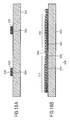
- FIG. 8 is a partial plan view of the display device to which the present invention is applied.
- FIG. 9 is a cross-sectional view taken along the line IX-IX of the display device illustrated in FIG. 8 ;
- FIG. 10 is a cross-sectional view taken along the line X-X of the display device illustrated in FIG. 8 ;
- FIG. 12 illustrates the manufacturing method for a display device according to the second embodiment of the present invention
- FIGS. 13A and 13B illustrate the manufacturing method for a display device according to the second embodiment of the present invention
- FIG. 14 illustrates a manufacturing method for a display device according to a third embodiment of the present invention.
- FIGS. 15A and 15B illustrate the manufacturing method for a display device according to the third embodiment of the present invention
- FIGS. 16A and 16B illustrate the manufacturing method for a display device according to the third embodiment of the present invention
- FIGS. 17A and 17B illustrate the manufacturing method for a display device according to the third embodiment of the present invention
- FIGS. 18A and 18B illustrate the manufacturing method for a display device according to the third embodiment of the present invention
- FIG. 19 illustrates the manufacturing method for a display device according to the third embodiment of the present invention.
- FIG. 20 illustrates the manufacturing method for a display device according to the third embodiment of the present invention.
- FIGS. 21A and 21B illustrate the manufacturing method for a display device according to the third embodiment of the present invention
- FIGS. 22A and 22B illustrate the manufacturing method for a display device according to the third embodiment of the present invention
- FIGS. 23A and 23B illustrate the manufacturing method for a display device according to the third embodiment of the present invention
- FIGS. 24A and 24B illustrate the manufacturing method for a display device according to the third embodiment of the present invention
- FIG. 25 is a partial plan view of the display device to which the present invention is applied.
- FIG. 26 is a cross-sectional view taken along the line XXVI-XXVI of the display device illustrated in FIG. 25 ;
- FIG. 27 is a cross-sectional view taken along the line XXVII-XXVII of the display device illustrated in FIG. 25 ;
- FIG. 28 illustrates a manufacturing method for a display device according to a fourth embodiment of the present invention.
- FIG. 29 illustrates the manufacturing method for a display device according to the fourth embodiment of the present invention.
- FIG. 30 illustrates the manufacturing method for a display device according to the fourth embodiment of the present invention.
- FIG. 31 illustrates the manufacturing method for a display device according to the fourth embodiment of the present invention.
- FIG. 32 illustrates the manufacturing method for a display device according to the fourth embodiment of the present invention.
- FIG. 33 illustrates the manufacturing method for a display device according to the fourth embodiment of the present invention.
- FIG. 35 illustrates the manufacturing method for a display device according to the fourth embodiment of the present invention.
- FIG. 36 is a partial plan view of the display device to which the present invention is applied.
- FIG. 37 is a cross-sectional view taken along the line 37 - 37 of the display device illustrated in FIG. 36 ;
- FIG. 38 is a cross-sectional view taken along the line 38 - 38 of the display device illustrated in FIG. 36 ;
- FIG. 39 illustrates a manufacturing method for a display device according to a fifth embodiment of the present invention.
- FIG. 40 illustrates the manufacturing method for a display device according to the fifth embodiment of the present invention.
- FIG. 42 illustrates the manufacturing method for a display device according to the fifth embodiment of the present invention.
- FIG. 43 illustrates the manufacturing method for a display device according to the fifth embodiment of the present invention.
- FIG. 44 illustrates the manufacturing method for a display device according to the fifth embodiment of the present invention.
- FIG. 45 illustrates the manufacturing method for a display device according to the fifth embodiment of the present invention.
- FIG. 47 illustrates the manufacturing method for a display device according to the fifth embodiment of the present invention.
- FIG. 48 illustrates the manufacturing method for a display device according to the fifth embodiment of the present invention.
- FIG. 49 illustrates the manufacturing method for a display device according to the fifth embodiment of the present invention.
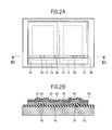
- FIG. 1B is a cross-sectional view taken along the line IB-IB of a structure illustrated in FIG. 1A .
- the substrate 10 is made of glass, for example, and is often required to have optical transparency.
- the substrate 10 is a mother substrate for manufacturing a plurality of display devices integrally.
- One substrate 10 has a plurality of product areas 12 (areas corresponding to display device components), and each of the product areas 12 has an effective display area 14 (image display area).
- the substrate 10 is a thin film transistor (TFT) substrate (or array substrate) including thin-film field-effect transistors, pixel electrodes, wirings, and the like.
- TFT thin film transistor
- the liquid crystal display panel may employ any drive mode, such as an in-plane switching (IPS) mode, a twisted nematic (TN) mode, and a vertical alignment (VA) mode, and electrodes and wirings are formed according to the mode.
- IPS in-plane switching
- TN twisted nematic
- VA vertical alignment
- the display device according to the present invention is not limited to the liquid crystal display panel, and may be an electroluminescent display device.
- a semiconductor layer 20 such as an amorphous silicon layer, is formed above the substrate 10 (on the gate insulating film 18 ).
- the semiconductor layer 20 is formed integrally over the plurality of product areas 12 .
- a source region, a drain region, and a channel region of each field-effect transistor are formed through the processes described later.
- the semiconductor layer 20 and the gate wirings 16 are electrically insulated from each other by the gate insulating film 18 .
- a metallic layer 22 is formed on the semiconductor layer 20 .
- the metallic layer 22 is also formed integrally over the plurality of product areas 12 .
- a source electrode 34 and a drain electrode 32 of each field-effect transistor are formed through the process ( FIG. 5 ) described later.
- FIG. 2B is a cross-sectional view taken along the line IIB-IIB of the structure illustrated in FIG. 2A .
- the etching resist 28 is formed by patterning a photoresist using photolithography.
- the difference in thickness between the first portion 24 and the second portion 26 may be formed by half-tone exposure in photolithographic exposure.
- FIG. 2A illustrates only a part of the etching resist 28 , and omits other parts thereof.
- the overall etching resist 28 including the first portions 24 and the second portions 26 is formed across the plurality of product areas 12 .
- the first portions 24 of the etching resist 28 are located on the metallic layer 22 corresponding to wiring portions.
- the second portion 26 being thin is located in a region (channel region) between the source electrode 34 and the drain electrode 32 of each field-effect transistor ( FIG. 5 ), as well as on an end of each product area 12 .
- the semiconductor layer 20 and the metallic layer 22 are patterned by etching.
- the etching of the two layers may be performed simultaneously (once) or separately (twice), depending on the type of etching.
- a wiring 30 is formed from the metallic layer 22 , and the semiconductor layer 20 is left under the wiring 30 .
- an electrical test (such as a test as for disconnection or short-circuit) is conducted on the wiring 30 .
- the wiring 30 extends continuously across the plurality of product areas 12 . Therefore, the electrical test on the plurality of product areas 12 may be conducted at a time.
- ashing is performed to thin the etching resist 28 so that the second portions 26 being thin may be removed while leaving the first portions 24 unremoved. This process may be performed after the electrical test or before the electrical test.
- the first portions 24 are located at least in respective regions for forming the source electrode 34 and the drain electrode 32 of each field-effect transistor ( FIG. 5 ). After the removal of the second portions 26 being thin, the wiring 30 is exposed from the etching resist 28 in part on the channel region of each field-effect transistor.
- the wiring 30 is also exposed from the etching resist 28 in part on the end of each product area 12 ( FIG. 3 ). Specifically, the wiring 30 is partially exposed from the etching resist 28 continuously from inside to outside the end of each product area 12 (along a cutting line of the substrate 10 ; see FIG. 7A ). The wiring 30 is partially exposed from the etching resist 28 at a position closer to each cutting line of the substrate 10 with respect to portions corresponding to the drain electrode 32 and the source electrode 34 ( FIG. 5 ).
- the wiring 30 is patterned.
- the patterning is performed through the first portions 24 of the etching resist 28 .
- the patterning is performed using selective etching, which etches the wiring 30 but leaves the semiconductor layer 20 unetched.
- the patterning enables the wiring 30 to be divided into the drain electrodes 32 and the source electrodes 34 .
- the wiring 30 is cut at the position closer to each cutting line of the substrate 10 with respect to the drain electrode 32 and the source electrode 34 .
- a portion of the wiring 30 located on the end of each product area 12 is removed by etching. In this case, the wiring 30 is etched, but the semiconductor layer 20 formed thereunder is left unetched. Then, the etching resist 28 is removed.
- a passivation film 36 such as a silicon oxide film or a silicon nitride film, is formed over the wiring 30 .
- FIG. 6B is a cross-sectional view taken along the line VIB-VIB of the structure illustrated in FIG. 6A .
- the passivation film 36 is formed of a semiconductor compound having insulating properties (such as SiO 2 or SiN).
- FIG. 7B is a cross-sectional view taken along the line VIIB-VIIB of the structure illustrated in FIG. 7A .
- the passivation film 36 , the wiring 30 , the semiconductor layer 20 , and the gate insulating film 18 are cut as well. In this way, individual TFT substrates are obtained.
- the substrate 10 may be cut after a counter substrate (color filter substrate) (not shown) is disposed at a distance from the substrate 10 with liquid crystal being sealed between the substrate 10 and the counter substrate. In this case, a display device is obtained.
- the wiring 30 is cut at the same time as an originally-defined process (process of forming the drain electrode 32 and the source electrode 34 ) (see FIG. 5 ). Therefore, an influence caused by exposed wirings 30 may be prevented without increasing the number of processes. For instance, in the example of FIGS. 7A and 7B , the cut surface of the wiring 30 is recessed with respect to the cutting line of the substrate 10 , and hence the cut surface may be sealed with ease.
- a part of the wiring 30 (right-hand side of FIG. 7B ) is cut to be recessed with respect to the cut surface of the substrate 10 , and the cut surface of the wiring 30 is covered with the passivation film 36 . Therefore, the drain electrode 32 and the source electrode 34 are prevented from being directly affected by static electricity or electrolytic corrosion, which may be caused by an exposed cut surface of the wiring 30 .
- the wiring 30 has another end to which the present invention is not applied, other than the end to which the present invention is applied.
- a part of the wiring 30 (left-hand side of FIG. 7B ) has another cut surface which is flush with the cut surface of the substrate 10 , showing that the present invention is not applied thereto.
- the part is covered with a sealing member (not shown).
- the present invention may be applied to all parts of the wiring 30 , in which each cut surface of the wiring 30 is positioned inside the cut surface of the substrate 10 .
- FIG. 8 is a partial plan view of the display device to which the present invention is applied.
- FIG. 9 is a cross-sectional view taken along the line IX-IX of the display device illustrated in FIG. 8 .
- FIG. 10 is a cross-sectional view taken along the line X-X of the display device illustrated in FIG. 8 .
- a wiring 130 is divided into a drain electrode 132 and a source electrode 134 .
- the drain electrode 132 is U-shaped so that the linear source electrode 134 enters the U-shape.
- FIG. 8 illustrates one drain electrode 132
- a plurality of the drain electrodes 132 are electrically connected by a wiring line 138 .
- the wiring line 138 extends continuously across a plurality of product areas.
- a semiconductor layer 120 Formed under the drain electrode 132 and the source electrode 134 is a semiconductor layer 120 , formed under the semiconductor layer 120 is a gate insulating film 118 , and formed under the gate insulating film 118 is a gate wiring 116 .
- the drain electrode 132 and the source electrode 134 are covered with a passivation film 136 , and a pixel electrode 140 is formed on the passivation film 136 .
- the pixel electrode 140 is electrically connected to the source electrode 134 via a through hole 142 formed in the passivation film 136 .
- FIG. 11A to FIG. 13B illustrate a manufacturing method for a display device according to a second embodiment of the present invention.
- the same processes as in the first embodiment are performed halfway. Specifically, the processes of the first embodiment described with reference to FIG. 1A to FIG. 6B (up to the process of forming the passivation film 36 over the wiring 30 after the patterning of the wiring 30 ) are performed. Then, the passivation film 36 is etched before the process of cutting the substrate 10 (see FIGS. 7A and 7B ).
- FIG. 11B is a cross-sectional view taken along the line XIB-XIB of the structure illustrated in FIG. 11A .
- the etching resist 228 has first openings 38 and second openings 40 , from which the passivation film 36 is exposed.
- the first openings 38 are formed above the wiring 30 corresponding to portions that need to be electrically connected.
- the second openings 40 are formed at a position crossing the end of each product area 12 (cutting line).
- the passivation film 36 is etched to form through holes 42 in the passivation film 36 , which are used for establishing electrical connection to the wiring 30 .
- This etching is performed through the first openings 38 of the etching resist 228 .
- a passing through hole (or notch) 44 is formed in the passivation film 36 by etching at a position closer to each cutting line of the substrate 10 with respect to the drain electrode 32 and the source electrode 34 .
- This etching is performed through the second openings 40 of the etching resist 228 .
- the semiconductor layer 20 formed under the passivation film 36 is etched.
- the semiconductor layer 20 concerned corresponds to apart of the semiconductor layer 20 which is left unprocessed after the cutting of the wiring 30 (see FIG. 5 ). This part is cut by etching. After that, the etching resist 228 is removed.
- FIG. 13B is a cross-sectional view taken along the line XIIIB-XIIIB of the structure illustrated in FIG. 13A .
- the passivation film 36 , the wiring 30 , the semiconductor layer 20 , and the gate insulating film 18 are cut as well. In this way, individual TFT substrates are obtained.
- the substrate 10 may be cut after a counter substrate (color filter substrate) (not shown) is disposed at a distance from the substrate 10 with liquid crystal being sealed between the substrate 10 and the counter substrate. In this case, a display device is obtained.
- the influence due to static electricity or electrolytic corrosion is further suppressed because the semiconductor layer 20 is also cut to be recessed with respect to the cut surface of the substrate 10 .
- Other details of the manufacturing method according to this embodiment correspond to the contents described in the first embodiment.
- the display device includes the substrate 10 , the semiconductor layer 20 formed above the substrate 10 , the wiring 30 formed in part on the semiconductor layer 20 , and the passivation film 36 covering the semiconductor layer 20 and the wiring 30 .
- the semiconductor layer 20 includes a first portion 224 and a second portion 226 , the first portion 224 being located under the wiring 30 , the second portion 226 protruding from the wiring 30 from the first portion 224 along a longitudinal direction of the wiring 30 .
- the passivation film 36 has a notch (or passing through hole) 46 formed therein.
- the second portion 226 of the semiconductor layer 20 has a leading end surface, which is flush with a plane of the notch (or passing through hole) 46 .
- Other details of the display device according to this embodiment encompass such a structure as is obvious from the above-mentioned manufacturing method.
- FIG. 14 to FIG. 24B illustrate a manufacturing method for a display device according to a third embodiment of the present invention.
- the display device to be manufactured in this embodiment is a liquid crystal display device using two oxide semiconductor layers, such as an in-plane switching (IPS) liquid crystal display device.
- IPS in-plane switching
- a first oxide conductive film 552 is formed on a substrate 510 .
- the first oxide conductive film 552 is formed of an oxide semiconductor having conductivity (such as indium tin oxide or indium zinc oxide).
- the first oxide conductive film 552 is a transparent conductive film.
- a first metallic layer 522 is formed on the first oxide conductive film 552 .
- FIGS. 15A and 15B are cross-sectional views taken along different lines in the same process. There are similar relationships between FIGS. 16A and 16B , FIGS. 17A and 17B , FIGS. 18A and 18B , FIGS. 21A and 21B , FIGS. 22A and 22B , and FIGS. 23A and 23B , respectively.
- an etching resist 528 is formed, which has first portions 524 being thick and second portions 526 being thin (the first portions 524 are thicker than the second portions 526 ).
- the first portions 524 of the etching resist 528 are located on the first metallic layer 522 corresponding to gate wirings 516 (see FIG. 16B ).
- the second portions 526 being thin are located above the first oxide conductive film 552 corresponding to common electrodes 554 (see FIG. 16A ).
- the second portions 526 are located also on an end of each product area 512 , which corresponds to the gate wiring 516 of the first metallic layer 522 .
- the first oxide conductive film 552 and the first metallic layer 522 are patterned by etching. Then, the common electrodes 554 are formed from the first oxide conductive film 552 .
- the gate wirings 516 are formed from the first metallic layer 522 .
- the first metallic layer 522 is left on the common electrode 554 .
- the first oxide conductive film 552 is left under the gate wiring 516 .
- ashing is performed to thin the etching resist 528 so that the second portions 526 being thin may be removed while leaving the first portions 524 unremoved. This process may be performed after the electrical test or before the electrical test.
- the patterned semiconductor layer 520 and a patterned signal wiring 550 on the semiconductor layer 520 are formed on the gate insulating film 518 . Further, a passivation film 536 is formed over the signal wiring 550 .
- the passivation film 536 is formed of a semiconductor compound having insulating properties (such as SiO 2 or SiN).
- the passivation film 536 is etched to form through holes 542 in the passivation film 536 , which are used for establishing electrical connection to the signal wiring 550 .
- a passing through hole (or notch) 544 is formed in communication with the passivation film 536 and the gate insulating film 518 at the second position P 2 , the passing through hole having a size containing a width of the first oxide semiconductor film 552 left at the second position P 2 .
- the second oxide conductive film 556 is etched to form a pixel electrode 548 .
- a portion of the first oxide conductive film 552 corresponding to the passing through hole (or notch) 544 is also etched to cut the first oxide conductive film 552 .
- the first oxide conductive film 552 formed under the gate wiring 516 is cut at the same time as an originally-defined process, and hence an influence caused by exposed gate wirings 516 and first oxide conductive film 552 may be prevented without increasing the number of processes.
- FIG. 24B is a cross-sectional view taken along the line XXIVB-XXIVB of the structure illustrated in FIG. 24A .
- a display device is obtained when a counter substrate (color filter substrate) (not shown) is disposed and then the substrate 510 and the counter substrate are cut.
- a counter substrate color filter substrate
- the display device includes the substrate 510 , the first oxide conductive film 552 , the gate wirings 516 formed from the first metallic layer 522 , the gate insulating film 518 covering the gate wirings 516 , the semiconductor layer 520 formed on the gate insulating film 518 , and the signal wirings 550 formed in part on the semiconductor layer 520 (see FIG. 23A ).
- the passivation film 536 covers the semiconductor layer 520 and the signal wirings 550 , and has the through holes 542 formed therein on the signal wirings 550 .
- the pixel electrode 548 formed from the second oxide conductive film 556 is formed on the passivation film 536 so as to be electrically connected to the signal wiring 550 via the through hole 542 .
- first oxide conductive film 552 Using the first oxide conductive film 552 , common electrodes 554 (see FIG. 18A ) facing the pixel electrodes 548 are formed. As illustrated in FIGS. 24A and 24B , the gate insulating film 518 and the passivation film 536 have a notch (or passing through hole) 546 formed therein in communication therewith. Respective leading end surfaces of the gate wiring 516 and the first oxide conductive film 552 formed thereunder are flush with a plane of the notch (or passing through hole) 546 .
- FIG. 25 is a partial plan view of the display device to which the present invention is applied.
- FIG. 26 is a cross-sectional view taken along the line XXVI-XXVI of the display device illustrated in FIG. 25 .
- FIG. 27 is a cross-sectional view taken along the line XXVII-XXVII of the display device illustrated in FIG. 25 .
- a wiring 330 is divided into a drain electrode 332 and a source electrode 334 .
- the drain electrode 332 is U-shaped so that the linear source electrode 334 enters the U-shape.
- FIG. 25 illustrates one drain electrode 332 , a plurality of the drain electrodes 332 are electrically connected by a wiring line 338 .
- a semiconductor layer 320 Formed under the drain electrode 332 and the source electrode 334 is a semiconductor layer 320 , formed under the semiconductor layer 320 is a gate insulating film 318 , and formed under the gate insulating film 318 is a gate wiring 316 .
- a gate wiring 316 Formed under the gate wiring 316 is a first oxide conductive film 352 .
- a common electrode 354 is formed of the same material in the same layer as those of the first oxide conductive film 352 (see FIG. 25 ).
- the drain electrode 332 and the source electrode 334 are covered with a passivation film 336 , and a pixel electrode 340 is formed on the passivation film 336 .
- the pixel electrode 340 is electrically connected to the source electrode 334 via a through hole 342 formed in the passivation film 336 .
- FIG. 28 to FIG. 35 illustrate a manufacturing method for a display device according to a fourth embodiment of the present invention.
- a substrate 710 is prepared.
- the substrate 710 is made of glass, for example, and is often required to have optical transparency.
- the substrate 710 is a mother substrate for manufacturing a plurality of display devices integrally.
- One substrate 710 has a plurality of product areas (areas corresponding to display device components), and each of the product areas has an effective display area (image display area).
- the substrate 710 is a thin film transistor (TFT) substrate (or array substrate) including thin-film field-effect transistors, pixel electrodes, wirings, and the like.
- TFT thin film transistor
- the liquid crystal display panel may employ any drive mode, such as an in-plane switching (IPS) mode, a twisted nematic (TN) mode, and a vertical alignment (VA) mode, and electrodes and wirings are formed according to the mode.
- IPS in-plane switching
- TN twisted nematic
- VA vertical alignment
- the display device according to the present invention is not limited to the liquid crystal display panel, and may be an electroluminescent display device.
- gate wirings 716 are formed on the substrate 710 .
- the gate wirings 716 serve in part as gate electrodes of the field-effect transistors.
- this embodiment describes a bottom-gate field-effect transistor, whose gate electrode is located downward.
- a gate insulating film 718 is formed over the gate wirings 716 .
- a semiconductor layer 720 such as an amorphous silicon layer, is formed above the substrate 710 (on the gate insulating film 718 ).
- the semiconductor layer 720 is patterned to have a source region, a drain region, and a channel region of each field-effect transistor. In the cross-section illustrated in FIG. 28 , the semiconductor layer 720 is formed only above each gate wiring 716 .
- the semiconductor layer 720 and the gate wirings 716 are electrically insulated from each other by the gate insulating film 718 .
- a wiring 730 is formed.
- the wiring 730 is patterned to be divided into source electrodes 732 and drain electrodes 734 .
- the patterning is performed by etching through an etching resist 728 .
- the etching resist 728 is formed by patterning a photoresist using photolithography.
- an electrical test is conducted on the wiring 730 .
- the wiring 730 extends continuously across the plurality of product areas, and adjacent drain electrodes 734 are electrically connected to each other, for example. Therefore, the electrical test on the plurality of product areas may be conducted at a time.
- a passivation film 736 is formed over the patterned wiring 730 .
- the passivation film 736 is formed of a semiconductor compound having insulating properties (such as SiO 2 or SiN).
- a metallic layer 722 is formed over the passivation film 736 and inside the through holes 742 on the wiring 730 .
- the metallic layer 722 is further formed inside the passing through holes (or notches) 744 on the wiring 730 .
- an etching resist 729 is formed in each region of the metallic layer 722 for forming a pixel electrode 748 (see FIG. 34 ).
- the metallic layer 722 is etched to form the pixel electrodes 748 .
- FIG. 34 illustrates only a part of the pixel electrode 748 .
- the portion of the wiring 730 corresponding to the passing through hole (or notch) 744 is further etched to cut the wiring 730 .
- the wiring 730 is cut at the same time as an originally-defined process, and hence an influence caused by exposed wirings 730 may be prevented without increasing the number of processes.
- the substrate 710 is cut.
- the passivation film 736 and the gate insulating film 718 are cut as well.
- a display device is obtained when a counter substrate (color filter substrate) (not shown) is disposed and then the substrate 710 and the counter substrate are cut.
- the display device includes the substrate 710 , the semiconductor layer 720 formed above the substrate 710 , and the wirings 730 formed in part on the semiconductor layer 720 .
- the passivation film 736 covers the semiconductor layer 720 and the wirings 730 , and has the through hole 742 formed therein at a position on the wiring 730 .
- the passivation film 736 has the notch (or passing through hole) 746 formed therein.
- the pixel electrode 748 is formed on the passivation film 736 so as to be electrically connected to the wiring 730 via the through hole 742 .
- a leading end surface of the wiring 730 is flush with a plane of the notch (or passing through hole) 746 of the passivation film 736 .
- Other details of the display device according to the present invention encompass such a structure as is obvious from the above-mentioned manufacturing method.
- FIG. 36 is a partial plan view of the display device to which the present invention is applied.
- FIG. 37 is a cross-sectional view taken along the line 37 - 37 of the display device illustrated in FIG. 36 .
- FIG. 38 is a cross-sectional view taken along the line 38 - 38 of the display device illustrated in FIG. 36 .
- a wiring 630 is divided into a drain electrode 632 and a source electrode 634 .
- the drain electrode 632 is U-shaped so that the linear source electrode 634 enters the U-shape.
- FIG. 36 illustrates one drain electrode 632 , a plurality of the drain electrodes 632 are electrically connected by a wiring line 638 .
- the wiring line 638 extends continuously across a plurality of product areas.
- a semiconductor layer 620 Formed under the drain electrode 632 and the source electrode 634 is a semiconductor layer 620 , formed under the semiconductor layer 620 is a gate insulating film 618 , and formed under the gate insulating film 618 is a gate wiring 616 .
- the drain electrode 632 and the source electrode 634 are covered with a passivation film 636 , and a pixel electrode 640 is formed on the passivation film 636 .
- the pixel electrode 640 is electrically connected to the source electrode 634 via a through hole 642 formed in the passivation film 636 .
- FIG. 39 to FIG. 49 illustrate a manufacturing method for a display device according to a fifth embodiment of the present invention.
- a gate wiring 816 is formed on a substrate 810 . Then, an electrical test is conducted on the gate wiring 816 .
- the gate wiring 816 extends continuously across a plurality of product areas 812 . Therefore, the electrical test on the plurality of product areas 812 may be conducted at a time.
- a gate insulating film 818 is formed over the gate wiring 816 .
- a patterned semiconductor layer 820 and a patterned signal wiring 850 formed on the semiconductor layer 820 are formed on the gate insulating film 818 .
- a passivation film 836 is formed over the signal wiring 850 .
- the passivation film 836 is formed of a semiconductor compound having insulating properties (such as SiO 2 or SiN).
- the passivation film 836 is etched to form through holes 842 in the passivation film 836 , which are each used for establishing electrical connection to the signal wiring 850 .
- a passing through hole (or notch) 844 is formed in communication with the passivation film 836 and the gate insulating film 818 , at a position of the gate wiring 816 closer to each cutting line of the substrate 810 with respect to the semiconductor layer 820 (see FIG. 49 ), the passing through hole having a size containing a width of the gate wiring 816 .
- a metallic layer 822 is formed over the passivation film 836 and inside the through holes 842 on the signal wiring 850 .
- the metallic layer 822 is further formed inside the passing through holes (or notches) 844 on the gate wiring 816 .
- the metallic layer 822 is etched to form a pixel electrodes 848 .
- a portion of the gate wiring 816 corresponding to the passing through hole (or notch) 844 is further etched to cut the gate wiring 816 .
- the gate wiring 816 is cut at the same time as an originally-defined process, and hence an influence caused by exposed gate wirings 816 may be prevented without increasing the number of processes.
- the substrate 810 is cut. In this way, individual TFT substrates are obtained, and a display device is obtained when a counter substrate (color filter substrate) (not shown) is disposed and then the substrate 810 and the counter substrate are cut.
- a counter substrate color filter substrate
- the display device includes the substrate 810 , the gate wirings 816 , the gate insulating film 818 covering the gate wirings 816 , the semiconductor layer 820 formed on the gate insulating film 818 , and the signal wirings 850 formed in part on the semiconductor layer 820 (see FIG. 47 ).
- the passivation film 836 covers the semiconductor layer 820 and the signal wirings 850 , and has the through holes 842 formed therein at the positions on the signal wirings 850 .
- the pixel electrode 848 is formed on the passivation film 836 so as to be electrically connected to the signal wiring 850 via the through hole 842 .
- the gate insulating film 818 and the passivation film 836 have a notch (or passing through hole) 846 formed therein in communication therewith (see FIG. 49 ).
- a leading end surface of the gate wiring 816 is flush with a plane of the notch (or passing through hole) 846 .
- Other details of the display device according to this embodiment encompass such a structure as is obvious from the above-mentioned manufacturing method.
- the present invention is not limited to the embodiments described above, and various modifications may be made thereto.
- the structures described in the embodiments may be replaced by a structure having substantially the same structure, a structure having the same action and effect, and a structure which may achieve the same object.
Landscapes
- Engineering & Computer Science (AREA)
- Power Engineering (AREA)
- Microelectronics & Electronic Packaging (AREA)
- Computer Hardware Design (AREA)
- Physics & Mathematics (AREA)
- Condensed Matter Physics & Semiconductors (AREA)
- General Physics & Mathematics (AREA)
- Manufacturing & Machinery (AREA)
- Ceramic Engineering (AREA)
- Liquid Crystal (AREA)
- Devices For Indicating Variable Information By Combining Individual Elements (AREA)
Abstract
Description
Claims (5)
Applications Claiming Priority (4)
| Application Number | Priority Date | Filing Date | Title |
|---|---|---|---|
| JP2009191313A JP5395566B2 (en) | 2009-08-20 | 2009-08-20 | Display device and manufacturing method thereof |
| JP2009191316A JP5324359B2 (en) | 2009-08-20 | 2009-08-20 | Display device and manufacturing method thereof |
| JP2009-191313 | 2009-08-20 | ||
| JP2009-191316 | 2009-08-20 |
Publications (2)
| Publication Number | Publication Date |
|---|---|
| US20110042675A1 US20110042675A1 (en) | 2011-02-24 |
| US8633491B2 true US8633491B2 (en) | 2014-01-21 |
Family
ID=43604596
Family Applications (1)
| Application Number | Title | Priority Date | Filing Date |
|---|---|---|---|
| US12/805,851 Active 2031-12-30 US8633491B2 (en) | 2009-08-20 | 2010-08-20 | Display device and manufacturing method thereof |
Country Status (1)
| Country | Link |
|---|---|
| US (1) | US8633491B2 (en) |
Citations (5)
| Publication number | Priority date | Publication date | Assignee | Title |
|---|---|---|---|---|
| JPH09138418A (en) | 1995-09-14 | 1997-05-27 | Citizen Watch Co Ltd | Liquid crystal matrix display panel inspecting method |
| JPH1020288A (en) | 1996-06-28 | 1998-01-23 | Optrex Corp | Stick substrate of liquid crystal display element |
| US20050092998A1 (en) * | 1999-02-12 | 2005-05-05 | Semiconductor Energy Laboratory Co., Ltd. | Semiconductor device, and method of forming the same |
| US20050170565A1 (en) * | 2004-01-29 | 2005-08-04 | Semiconductor Energy Laboratory Co., Ltd. | Forming method of contact hole, and manufacturing method of semicondutor device, liquid crystal display device and EL display device |
| US20050208710A1 (en) * | 2001-11-28 | 2005-09-22 | Semiconductor Energy Laboratory Co., Ltd. | Method of manufacturing a semiconductor device |
-
2010
- 2010-08-20 US US12/805,851 patent/US8633491B2/en active Active
Patent Citations (5)
| Publication number | Priority date | Publication date | Assignee | Title |
|---|---|---|---|---|
| JPH09138418A (en) | 1995-09-14 | 1997-05-27 | Citizen Watch Co Ltd | Liquid crystal matrix display panel inspecting method |
| JPH1020288A (en) | 1996-06-28 | 1998-01-23 | Optrex Corp | Stick substrate of liquid crystal display element |
| US20050092998A1 (en) * | 1999-02-12 | 2005-05-05 | Semiconductor Energy Laboratory Co., Ltd. | Semiconductor device, and method of forming the same |
| US20050208710A1 (en) * | 2001-11-28 | 2005-09-22 | Semiconductor Energy Laboratory Co., Ltd. | Method of manufacturing a semiconductor device |
| US20050170565A1 (en) * | 2004-01-29 | 2005-08-04 | Semiconductor Energy Laboratory Co., Ltd. | Forming method of contact hole, and manufacturing method of semicondutor device, liquid crystal display device and EL display device |
Also Published As
| Publication number | Publication date |
|---|---|
| US20110042675A1 (en) | 2011-02-24 |
Similar Documents
| Publication | Publication Date | Title |
|---|---|---|
| EP3483926B1 (en) | Method for manufacturing an array substrate of an ffs type tft-lcd | |
| EP2565917B1 (en) | Manufacturing method for array substrate with fringe field switching type thin film transistor liquid crystal display | |
| EP2071394B1 (en) | Active matrix substrate and liquid crystal display device provided with same | |
| US8497966B2 (en) | FFS type TFT-LCD array substrate and manufacturing method thereof | |
| KR101294232B1 (en) | Fringe field switching mode liquid crystal display device and the method for fabricating the same | |
| US7649586B2 (en) | Display device with floating transistor elements on alternating data lines | |
| US9524992B2 (en) | Thin film transistor array panel and manufacturing method thereof | |
| US8031285B2 (en) | Thin film transistor substrate, method of manufacturing the same, and liquid crystal display panel having the same | |
| KR20080059889A (en) | An array substrate of thin film transistor liquid crystal display device and the method for fabricating thereof | |
| KR102071008B1 (en) | Thin film transistor array panel and manufacturing method thereof | |
| US20150028340A1 (en) | Thin film transistor array substrate and manufacturing method thereof, and liquid crystal display device and manufacturing method thereof | |
| JP2012018970A (en) | Thin film transistor array substrate, manufacturing method of the same and liquid crystal display device | |
| KR20060135502A (en) | Electro-optic display and manufacturing method thereof | |
| KR20110008639A (en) | Thin film transistor panel and method of manufacturing the same | |
| US9257454B2 (en) | Thin film transistor array substrate | |
| US9741861B2 (en) | Display device and method for manufacturing the same | |
| US8743328B2 (en) | Manufacturing method for a liquid crystal display device wherein each side of a metal pattern and a semiconductor pattern facing an etched space is contacted by an insulating layer | |
| JP2020010030A (en) | Active matrix substrate and manufacturing method of active matrix substrate | |
| KR102461634B1 (en) | Liquid crystal display device and manufacturing method thereof | |
| US8633491B2 (en) | Display device and manufacturing method thereof | |
| JP5395566B2 (en) | Display device and manufacturing method thereof | |
| JP2014149410A (en) | Thin film transistor array substrate and method for manufacturing the same | |
| KR20140013522A (en) | Thin film transistor, liquid crystal display device and method of fabricating thereof | |
| JP5324359B2 (en) | Display device and manufacturing method thereof | |
| KR20150023160A (en) | Thin film transistor array panel and manufacturing method thereof |
Legal Events
| Date | Code | Title | Description |
|---|---|---|---|
| AS | Assignment |
Owner name: IPS ALPHA TECHNOLOGY, LTD., JAPAN Free format text: ASSIGNMENT OF ASSIGNORS INTEREST;ASSIGNORS:KAWAMURA, TETSUYA;SATO, MASASHI;WATANABE, YOSHIKI;AND OTHERS;SIGNING DATES FROM 20100413 TO 20100526;REEL/FRAME:024928/0876 |
|
| AS | Assignment |
Owner name: PANASONIC LIQUID CRYSTAL DISPLAY CO., LTD., JAPAN Free format text: CHANGE OF NAME;ASSIGNOR:IPS ALPHA TECHNOLOGY, LTD.;REEL/FRAME:026257/0377 Effective date: 20101001 |
|
| STCF | Information on status: patent grant |
Free format text: PATENTED CASE |
|
| FEPP | Fee payment procedure |
Free format text: PAYOR NUMBER ASSIGNED (ORIGINAL EVENT CODE: ASPN); ENTITY STATUS OF PATENT OWNER: LARGE ENTITY |
|
| FPAY | Fee payment |
Year of fee payment: 4 |
|
| MAFP | Maintenance fee payment |
Free format text: PAYMENT OF MAINTENANCE FEE, 8TH YEAR, LARGE ENTITY (ORIGINAL EVENT CODE: M1552); ENTITY STATUS OF PATENT OWNER: LARGE ENTITY Year of fee payment: 8 |
|
| AS | Assignment |
Owner name: PANASONIC INTELLECTUAL PROPERTY CORPORATION OF AMERICA, CALIFORNIA Free format text: NUNC PRO TUNC ASSIGNMENT;ASSIGNOR:PANASONIC LIQUID CRYSTAL DISPLAY CO., LTD.;REEL/FRAME:065615/0327 Effective date: 20230828 |