EP2067065B1 - Beleuchtungssystem, leuchte und anzeigevorrichtung - Google Patents
Beleuchtungssystem, leuchte und anzeigevorrichtung Download PDFInfo
- Publication number
- EP2067065B1 EP2067065B1 EP07826371.2A EP07826371A EP2067065B1 EP 2067065 B1 EP2067065 B1 EP 2067065B1 EP 07826371 A EP07826371 A EP 07826371A EP 2067065 B1 EP2067065 B1 EP 2067065B1
- Authority
- EP
- European Patent Office
- Prior art keywords
- light
- recesses
- illumination system
- emitting
- transmitting panel
- Prior art date
- Legal status (The legal status is an assumption and is not a legal conclusion. Google has not performed a legal analysis and makes no representation as to the accuracy of the status listed.)
- Not-in-force
Links
Images


Classifications
-
- G—PHYSICS
- G02—OPTICS
- G02B—OPTICAL ELEMENTS, SYSTEMS OR APPARATUS
- G02B6/00—Light guides; Structural details of arrangements comprising light guides and other optical elements, e.g. couplings
- G02B6/0001—Light guides; Structural details of arrangements comprising light guides and other optical elements, e.g. couplings specially adapted for lighting devices or systems
- G02B6/0011—Light guides; Structural details of arrangements comprising light guides and other optical elements, e.g. couplings specially adapted for lighting devices or systems the light guides being planar or of plate-like form
- G02B6/0033—Means for improving the coupling-out of light from the light guide
- G02B6/0035—Means for improving the coupling-out of light from the light guide provided on the surface of the light guide or in the bulk of it
- G02B6/004—Scattering dots or dot-like elements, e.g. microbeads, scattering particles, nanoparticles
-
- G—PHYSICS
- G02—OPTICS
- G02B—OPTICAL ELEMENTS, SYSTEMS OR APPARATUS
- G02B6/00—Light guides; Structural details of arrangements comprising light guides and other optical elements, e.g. couplings
- G02B6/0001—Light guides; Structural details of arrangements comprising light guides and other optical elements, e.g. couplings specially adapted for lighting devices or systems
- G02B6/0011—Light guides; Structural details of arrangements comprising light guides and other optical elements, e.g. couplings specially adapted for lighting devices or systems the light guides being planar or of plate-like form
- G02B6/0033—Means for improving the coupling-out of light from the light guide
- G02B6/0035—Means for improving the coupling-out of light from the light guide provided on the surface of the light guide or in the bulk of it
- G02B6/0036—2-D arrangement of prisms, protrusions, indentations or roughened surfaces
Definitions
- the invention relates to an illumination system comprising a light source and a light-transmitting panel comprising a light-emitting window, a rear wall situated opposite said light-emitting window, and edge walls extending between the light-emitting window and the rear wall.
- the invention also relates to a luminaire and a display device.
- Such illumination systems are known per se. They are used, inter alia, as luminaires for general lighting purposes, for example, for office lighting or shop lighting, for example, shop-window lighting or lighting of (transparent or semi-transparent) plates of glass or of (transparent) synthetic resin on which, for example, jewelry is displayed.
- An alternative application is the use of such systems for illuminating billboards.
- Such known illumination systems are also used as backlight-emitting panels in (picture) display devices, for example, for TV sets and monitors. These systems are particularly suitable for use as backlights for non-emissive displays such as liquid crystal display devices, also referred to as LCD panels, which are used in (portable) computers or (portable) telephones.
- non-emissive displays such as liquid crystal display devices, also referred to as LCD panels, which are used in (portable) computers or (portable) telephones.
- These display devices usually comprise a substrate provided with a regular pattern of pixels, each of which is controlled by at least one electrode.
- the display device utilizes a control circuit for achieving a picture or a data-graphical display in a relevant field of a (picture) screen of the (picture) display device.
- the light originating from the backlight in an LCD device is modulated by means of a switch or modulator, using various types of liquid crystal effects.
- the display may be based on electrophoretic or electromechanical effects.
- the illumination system mentioned in the opening paragraph comprises a light-emitting diode (further also referred to as LED).
- This LED maybe provided in the vicinity of or tangent to a light-transmitting edge surface of the light-emitting panel, in which case light originating from the light source is incident on the light-transmitting edge surface during operation and distributes itself in the panel.
- the illumination system comprises a plurality of LEDs, which may be distributed on the rear wall of the light-transmitting panel.
- the illumination system comprises a plurality of LEDs and a light guide plate.
- the LEDs are arranged for direct illumination of the image display device in a regular array.
- the light guide plate is arranged between the regular array of LEDs and the image display device and has a plurality of recesses, each recess comprising a LED from the plurality of LEDs.
- the known illumination system has the disadvantage that the light-emitting window has a relatively poor uniformity throughout.
- an illumination system comprising:
- the effect of the measures according to the invention is that the light emitted by the at least one light source is coupled out from the light-transmitting panel of the illumination system via scattering material in the recesses which are distributed substantially regularly on the rear wall.
- the light emitted by the at least one light source is coupled into the light-transmitting panel and travels through the light-transmitting panel via total internal reflection between the light-emitting window and the rear wall. Due to confinement of the light in the light-transmitting panel, the light emitted by the at least one light source is mixed and distributed substantially uniformly in the light-transmitting panel.
- the sub-set of recesses is distributed substantially regularly on the rear wall, resulting in a substantially regular distribution of the scattering material on the rear wall.
- the plurality of light-emitting diodes (further also referred to as LEDs) is arranged in a matrix for direct illumination of the image display device.
- the light guide plate is arranged between the plurality of LEDs and the image display device to distribute the light on part of the area of the light guide plate.
- the uniformity of light emission throughout the matrix of LEDs is relatively poor, resulting in a relatively poor uniformity of the light emitted from the light guide plate to the image display device.
- the rear wall of the light-emitting panel comprises the sub-set of recesses, which comprise scattering material.
- the recesses of the sub-set are distributed substantially regularly on the rear wall, which results in a substantially regular distribution of the scattering material on the rear wall.
- the pitch of the lenticular elements is such that all light emitted from a single recess is captured by a single lenticular element.
- the light emitted from the luminaire must be shielded in accordance with predefined regulations.
- Such complementary arrangement of lenticular beam-shaping element determines the angular distribution of the light emitted by the illumination system and which is in accordance with said predefined regulations.
- the illumination system according to the invention has the further advantage that direct glare from the illumination system is prevented.
- Direct glare is a visual discomfort resulting from insufficiently shielded light sources.
- the light source of the luminaire should preferably not be directly visible or should be shielded in accordance with predefined regulations.
- the emitted light results from confined light from the light-transmitting panel being scattered from the light-transmitting panel through the light-emitting window.
- the light emitted by the at least one light source is substantially confined and mixed inside the light-transmitting panel and substantially only emitted from the light-transmitting panel via the scattering material. Due to this arrangement, the at least one light source is not directly visible when viewing the illumination system via the light-emitting window and, as such, direct glare from the illumination system is prevented.
- the scattering material comprises a luminescent material absorbing light of the predominant wavelength and emitting light of a further predominant wavelength.
- a luminescent material absorbing light of the predominant wavelength and emitting light of a further predominant wavelength.
- This embodiment has the advantage that the claimed arrangement of the luminescent material allows a relatively broad range of luminescent materials to be used in the illumination system according to the invention.
- luminescent materials which determine the further predominant wavelength emitted by the known illumination systems are directly applied to the light source, for example, on light-emitting diodes, or, for example, on high-pressure gas discharge lamps.
- the choice of luminescent materials to be directly applied to the light source is limited, because these materials must be able to withstand, in operation, a relatively high temperature of the light source and at the same time withstand, in operation, a relatively high light-energy flux emitted by the light source. Nevertheless, the high temperature and high light-energy flux generally result in a gradual degradation of the luminescent material, gradually reducing the efficiency of the illumination system.
- the luminescent material is applied away from the light source in the sub-set of recesses. This arrangement of the luminescent material reduces the requirements of the luminescent material to withstand the high temperature and the high light-energy flux, and, in addition, reduces the gradual degradation of the luminescent material.
- Light of a predominant wavelength comprises light of a predefined spectral bandwidth around a center wavelength.
- a LED emitting light of the predominant wavelength Blue emits light at the center wavelength of, for example, 470 nm, having a spectral bandwidth of, for example, 10 nm.
- Another example of light of a predominant wavelength from a LED is light of the predominant wavelength UV, having the central wavelength of, for example, 405 nm, and a spectral bandwidth of, for example, 5 nm.
- Red, Green and Blue a full-color image (including white) can be generated by the illumination system, for example, when this system is applied in a display device.
- other combinations of light of predominant wavelengths may be used in the illumination system, for example, Red, Green, Blue, Cyan, Yellow and White.
- the scattering material comprises a mixture of a plurality of luminescent materials, each luminescent material absorbing light of the predominant wavelength and emitting light of a further predominant wavelength.
- a mixture of luminescent materials can be chosen so that a sum of the different further predominant wavelengths of the different luminescent materials covers a major part of the visible electromagnetic spectrum, resulting in an illumination system having a relatively high color-rendering index.
- This embodiment is especially beneficial in general illumination applications in which a relatively high color-rendering index is generally required to obtain a true reproduction of a color of an object when illuminated by the illumination system.
- the illumination system further comprises a beam-shaping element arranged substantially parallel to the light-emitting window for generating a predefined angular distribution of the light emitted from the light-transmitting panel.
- the predefined angular distribution can be adapted, for example, by using the beam-shaping element to match the angular distribution required in a general lighting system such as a luminaire.
- the light emitted from the luminaire must be shielded in accordance with predefined regulations, for example, for reducing glare from the luminaire.
- the predefined regulations prescribe the angular distribution of the light emitted from the luminaire to be limited to within, for example, 60° from an axis arranged perpendicularly to the light-emitting window.
- the beam-shaping elements are an array of lenticular elements or, for example, an array of Fresnel-lens elements.
- the lenticular elements or Fresnel-lens elements are arrangedin an array which is complementary to the two-dimensional array of recesses.
- substantially each recess in the array of recesses is constituted by an emission wall and a side wall extending between the emission wall and the rear wall, the emission wall being arranged substantially parallel to the light-emitting window.
- the form and the dimensions of the emission wall together with the side wall contribute to the emission characteristic of the light-emitting panel.
- the emission wall and the side wall of the recess are arranged substantially perpendicularly.
- Light, which is scattered from the scattering material through the emission wall will generally be emitted by the light-transmitting panel via the light-emitting window, and light which is scattered from the scattering material through the side walls will generally be re-confined in the light-transmitting panel.
- the substantially perpendicular arrangement of the emission wall and the side walls results in a clear separation of the light from the scattering material which is emitted by the light-emitting panel and the light from the scattering material which is confined inside the light-emitting panel.
- the light source is constituted by a plurality of light-emitting diodes and a plurality of light entrance windows, wherein the plurality of light-emitting diodes is arranged in a further sub-set of further recesses of the two-dimensional array of recesses, the further recesses constituting the plurality of light entrance windows.
- This embodiment has the advantage that a single substrate arranged parallel to the rear wall can be used for mounting the light-emitting diodes and for applying the scattering material. This simplifies the construction of the illumination system and typically reduces production costs.
- This embodiment has the further advantage that the light emitted by the plurality of LEDs is mixed inside the light-transmitting panel and distributed substantially uniformly in the light-transmitting panel.
- the light from the LEDs is coupled out via the scattering material in the sub-set of recesses. Differences or variations of emitted intensity and/or color between the different LEDs are mixed inside the light-transmitting panel, which improves the uniformity of the light emitted by the light-transmitting panel and precludes the need for binning the LEDs.
- the plurality of light-emitting diodes are side-emitting light-emitting diodes arranged in the further sub-set of further recesses, the side-emitting light-emitting diodes being arranged to emit light, in operation, substantially parallel to the light-emitting window.
- Use of side-emitting LEDs has the advantage that the further recesses may be identical to the recesses comprising scattering material.
- Use of LEDs other than side-emitting LEDs generally requires the further recesses to include arrangements ensuring that the light from the LEDs is coupled into the light-transmitting panel, such that the in-coupled light is subsequently transported through the light-transmitting panel via total internal reflection.
- Such arrangements may include, for example, a specific shape of an emission wall of the further recesses of the further sub-set.
- Use of side-emitting LEDs allows both the recesses comprising scattering material and the further recesses to be identical, resulting in a simplification of the light-transmitting panel and typically a reduction of production costs.
- the further recesses of the further sub-set are mixed with the recesses of the sub-set, the mix of recesses and further recesses being distributed substantially regularly on the rear wall.
- This embodiment has the advantage that the LEDs are regularly distributed on the rear wall, thus allowing easier cooling of the LEDs.
- the distribution of the LEDs and of the scattering material in the two-dimensional array of recesses can be easily adapted without changing the light-transmitting panel. This allows easy alteration of the emission characteristic of the light-transmitting panel.
- the invention also relates to a luminaire and a display device comprising the illumination system according to the invention.
- US5779338A discloses a surface light source using a light conducting member in which a multiplicity of concave portions are formed on an opposite surface of a light emitting surface, said concave portions being filled with a light diffusing material.
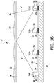
- Figs. 1A and 1B are cross-sectional views of an illumination system 2, 4 according to the invention.
- the illumination system 2, 4 comprises at least one light source, for example, a light-emitting diode 8, 10 (further also referred to as LED) for emitting light of a predominant wavelength R, G, B, UV, W, for example, the predominant wavelength White W (see Fig. 1A ) or, for example, the predominant wavelength Ultraviolet UV (see Fig. 2 ).
- the illumination system 2, 4 further comprises a light-transmitting panel 14 which comprises a light-emitting window 16, a rear wall 18 situated opposite said light-emitting window 16, and edge walls 20 extending between the light-emitting window 16 and the rear wall 18.
- the light-transmitting panel 14 is arranged to couple at least part of the light W emitted by the LED 8, 10 into the light-transmitting panel 14. This can be done, for example, via the edge wall 20 comprising, for example, a light entrance window 21 (see Fig. 1A ) or, for example, via a side wall 38 of a further recess 24 (see Fig. 1B ).
- the light W in the light-transmitting panel 14 is transported substantially via total internal reflection between the light-emitting window 16 and the rear wall 18.
- the rear wall 18 is provided with a two-dimensional array (see Fig. 1C ) of recesses 22, 24. A sub-set of recesses 22 is distributed substantially regularly on the rear wall 18.
- Each recess 22A, 22B, 22C, 22D of the sub-set 22 comprises scattering material 26, for example, particles of titanium oxide (TiO 2 ), or aluminum oxide (Al 2 O 3 ), or tantalum oxide (Ta 2 O 5 ), for coupling out the light W from the light-transmitting panel 14 through the light-emitting window 16.
- scattering material 26 for example, particles of titanium oxide (TiO 2 ), or aluminum oxide (Al 2 O 3 ), or tantalum oxide (Ta 2 O 5 ), for coupling out the light W from the light-transmitting panel 14 through the light-emitting window 16.
- the light W penetrates the particular recess 22A, 22B, 22C, 22D and is scattered by the scattering material 26.
- part of the scattered light W' will be coupled out from the light-transmitting panel 14 and part will be re-confined in the light-transmitting panel 14 via total internal reflection.
- the regular distribution of the scattering material 26 on the rear wall 18 improves the uniformity of the light W' emitted via the light-emitting window 16.
- Each recess 22A, 22B, 22C, 22D, 24A, 24B (see Figs. 2 and 3 ) in the two-dimensional array of recesses 22, 24 comprises an emission wall 36 and a side wall 38 arranged between the emission wall 36 and the rear wall 18.
- the light W' scattered away from the recess 22A, 22B, 22C, 22D via the emission wall 36 will generally be emitted by the light-transmitting panel 14, and light W' scattered away from the recess 22A, 22B, 22C, 22D via the side wall 38 is typically re-confined in the light-transmitting panel 14 and will generally be coupled out of the light-transmitting panel 14 via a subsequent recess 22A, 22B, 22C, 22D of the sub-set of recesses 22. This results in a clear separation of that part of the scattered light W' which is emitted by the light-transmitting panel 14 and that part of the scattered light W' which is re-confined inside the light-transmitting panel 14.
- Figs. 1A and 1B show a substrate 15 on which, for example, the scattering material 26 is applied.
- the scattering material may be deposited in the recesses 22A, 22B, 22C, 22D of the sub-set of recesses 22.
- the LED 10 may also be applied, for example, on the substrate 15, in which case the substrate 15 preferably comprises electric contacts (not shown) to supply power to the LED 10.
- the substrate 15 may be a flex-foil or a printed circuit board and is preferably at least partially specularly reflective to recycle the light that is scattered by the scattering material 26 in the direction of the substrate 15 back towards the light-emitting window 16.
- Light of a predominant wavelength R, G, B, UV, W comprises light of a predefined spectral bandwidth around a center wavelength.
- a LED 8, 10 emitting light of the predominant wavelength Blue B (not shown) emits light at the center wavelength of, for example, 470 nm, having a spectral bandwidth of, for example, 10 nm.
- Another example of light of a predominant wavelength from a LED 8, 10 is light of the predominant wavelength UV (see Fig. 2 ) having the central wavelength of, for example, 405 nm, and a spectral bandwidth of, for example, 5 nm.
- Red R (not shown), Green G (not shown) and Blue B
- a full-color image (including white) can be generated by the illumination system 2, 4, for example, when the illumination system 2, 4 is applied in a display device 50 (see Fig. 5 ).
- other combinations of light of predominant wavelengths R, G, B, UV, W may be used in the illumination system 2, 4, for example, Red R, Green G, Blue B, Cyan C (not shown), Yellow Y (not shown) and White W.
- Fig. 1A shows an embodiment of the illumination system 2, in which the LED 8 is arranged at the edge wall 20 of the light-transmitting panel 14.
- the edge wall 20 comprises, for example, the light entrance window 21 for coupling in the light W emitted by the LED 8.
- the remainder of the edge wall 20 of the light-transmitting panel 14 is reflective to confine the light W inside the light-transmitting panel 14.
- Fig. 1 ⁇ shows a beam of light W emitted by the LED 8. This beam of light W is reflected from the light-emitting window 16 via total internal reflection and, after reflection, reaches one particular recess 22A, 22B, 22C, 22D of the sub-set of recesses 22 and enters this particular recess 22A, 22B, 22C, 22D.
- the light W reaches the scattering material 26 in the particular recess 22A, 22B, 22C, 22D which scatters the light W, changing a direction of propagation of the light beam W, for example, into the light beam W'.
- the scattered light beam W' is emitted via the emission wall 36 of the particular recess 22A, 22B, 22C, 22D, via the light-emitting window 16, away from the light-transmitting panel 14.
- Fig. 1B shows an embodiment of the illumination system 4 which comprises at least one side-emitting LED 10 arranged in a further sub-set of further recesses 24.
- the illumination system 4 preferably comprises a plurality of side-emitting LEDs (see Fig. 1C ) arranged in the further recesses 24A, 24B of the further sub-set 24, regularly distributed between the sub-set of recesses 22.
- the side-emitting LEDs emit light substantially parallel to the light-emitting window 16 via the side wall 38 of a further recess 24A, 24B.
- FIG. 1B again shows a beam of light W emitted by the LED 10.
- This beam of light W is reflected from the light-emitting window 16 via total internal reflection and enters the particular recess 22A, 22B, 22C, 22D.
- the light W is scattered by the scattering material 26 in the particular recess 22A, 22B, 22C, 22D.
- the scattered light beam W' is emitted via the emission wall 36 of the recess 22A, 22B, 22C, 22D, via the light-emitting window 16 and via a beam-shaping element 30, away from the light-transmitting panel 14.
- the illumination system 2, 4 according to the invention shown in Fig. 1B comprises the beam-shaping element 30.
- the beam-shaping element 30 is preferably arranged substantially parallel to the light-emitting window 16 of the light-transmitting panel 14.
- a small gap 33 is arranged between the beam-shaping element 30 and the light-transmitting panel 14.
- the gap 33 may be filled, for example, with air or with a material having a specific refractive index, which ensures that the light W inside the light-transmitting panel 14 is substantially confined via total internal reflection.
- the beam-shaping element 30 is constituted by a material having the specific refractive index, in which case the gap 33 shown in Figs.
- the beam-shaping element 30 may be directly applied to the light-emitting window 16.
- the beam-shaping element 30 generates a predefined angular distribution 32 (see Fig. 4 ) of the light W' which is emitted from the light-transmitting panel 14.
- the predefined angular distribution 32 for example, matches the angular distribution 32 required in a general lighting system such as a luminaire 40 (see Fig. 5 ).
- a luminaire 40 the light W' emitted from the luminaire 40 must be shielded in accordance with predefined regulations, for example, for reducing glare from the luminaire 40.
- the predefined regulations prescribe the angular distribution 32 of the light emitted from the luminaire 40 to be limited to within, for example, 60° from an axis 34 (see Fig. 4 ) arranged perpendicularly to the light-emitting window 16.
- the beam-shaping element 30 maybe, for example an array of lenticular elements 30 or, for example, an array of Fresnel-lens elements (not shown).
- the lenticular elements 30 or Fresnel-lens elements are arrangedin an array complementary to the sub-set of recesses 22 (see Fig. 1C ).
- the emission wall 36 of the recesses 22A, 22B, 22C, 22D may be convex (not shown) or concave (not shown) so as to constitute a further beam-shaping element.
- the sub-set of recesses 22 and the further sub-set of further recesses 24 are identical recesses 22A, 22B, 22C, 22D, 24A, 24B.
- This embodiment has the advantage that the production of the light-transmitting panel is simplified. It has the further advantage that the distribution of the recesses 22A, 22B, 22C, 22D and the further recesses 24A, 24B can be easily changed without changing the light-transmitting panel 14, for example, by changing the distribution of the LEDs 10 and/or scattering material 26 on the substrate 15. Changing the distribution of the recesses 22A, 22B, 22C, 22D and the further recesses 24A, 24B, for example, changes a light emission characteristic of the illumination system 2, 4.
- the illumination system 2, 4 comprises LEDs arranged both at the edge wall 20 and in the further sub-set of recesses 24.
- Fig. 1C is a top view of an illumination system 4 according to the invention.
- the sub-sets of recesses 22 comprising the scattering material 26 are distributed substantially regularly across the light-transmitting panel 14.
- Fig. 1C further shows the beam-shaping element 30 constituted by an array of lenticular elements 30 arranged in an array complementary to the two-dimensional array of recesses 22, 24.
- Fig. 2 is a cross-sectional view of a further embodiment of the illumination system 6 according to the invention.
- the illumination system 6 comprises a plurality of LEDs arranged in the further sub-set of further recesses 24 mixed with the sub-set of recesses 22, identical to the illumination system 4 shown in Figs. 1B and 1C .
- the LEDs 10 arranged in the further recesses 24A, 24B are preferably side-emitting LEDs 10 emitting light of the predominant wavelength, for example, Ultraviolet UV.
- the recesses 22A, 22B, 22C, 22D comprise a luminescent material 28 which, for example, absorbs the light of the predominant wavelength Ultraviolet UV and emits light of a further predominant wavelength, for example, Red R (indicated by a broken line in Fig. 2 ).
- luminescent material is directly applied to LEDs so as to change the predominant wavelength emitted by a LED into a further predominant wavelength.
- This luminescent material must be able to withstand, in operation, a relatively high temperature of the LED, and at the same time withstand, in operation, a relatively high light-energy flux emitted by the LED.
- the luminescent material 28 is arranged in the recesses 22A, 22B, 22C, 22D of the sub-set of recesses 22.
- the luminescent material 28 absorbs light of the predominant wavelength Ultraviolet UV and emits light of the further predominant wavelength Red R.
- the luminescent material 28 is located remotely from the LEDs 10, which relaxes the need for the luminescent material 28 to withstand a relatively high temperature and a relatively high light-energy flux. Because of these relaxed temperature and light-energy flux requirements, an increased range of different luminescent materials 28 may be used in the arrangement shown in Fig. 2 . Furthermore, a relatively high temperature and a relatively high light-energy flux generally result in a gradual degradation of the luminescent material 28. The arrangement shown in Fig. 2 reduces the gradual degradation of the luminescent material 28, increasing the lifetime of the illumination system 8.
- the illumination system 2, 4, 6 mixes the light W, UV emitted by the plurality of LEDs 8, 10 inside the light-transmitting panel 14.
- This mixing of light W, UV in the light-transmitting panel 14 has the advantage that differences between the LEDs 8, 10 in the plurality of LEDs 8, 10 are substantially not visible, thus precluding the need for binning the LEDs 8, 10.
- the emission of the light W', R over the light-emitting window 16 remains substantially uniform, even when, for example, one of the LEDs 8, 10 in the plurality of LEDs 8, 10 fails.
- the uniformity of the light W', R emitted by the light-transmitting panel 14 is mainly determined by the distribution of the sub-set of recesses 22 comprising the scattering material 26 or the luminescent material 28, and is determined by a uniform distribution of the scattering material 26 or luminescent material 28 in each recess 22A, 22B, 22C, 22D.
- the scattering material 26 or luminescent material 28 can be applied substantially uniformly by using well-known methods such as screen printing, inkjet printing or electrophoretic coating.
- Figs. 3A, 3B, 3C and 3D are cross-sectional views ( Figs. 3A and 3C ) and top views ( Figs. 3B and 3D ) of one further recess 24A of the further sub-set of further recesses 24 arranged in the light-transmitting panel 14 comprising a LED 10.
- the further recess 24A is a cylindrically shaped further recess 24A comprising the side-emitting LED 10.
- the side wall 38 is arranged substantially perpendicularly to the emission wall 36 of the further recess 24A.
- the side-emitting LED 10 emits light W substantially in all directions parallel to the light-emitting window 16 of the light-transmitting panel 14. Substantially the only light passing from the further recess 24A into the light-transmitting panel 14 via the emission wall 36 is stray light, resulting, for example, from reflections inside the further recess 24A.
- the further recess 24A is a cube-shaped further recess 24A comprising the side-emitting LED 12.
- the side-emitting LED 12 emits light W substantially in one direction parallel to the light-emitting window 16 of the light-transmitting panel 14.
- a further recess 24C comprising a side-emitting LED 12 which substantially emits light only in one direction preferably comprises a reflecting surface 25 at the sides of the cube-shaped further recess 24C which is not used for emitting light into the light-transmitting panel 14.
- the reflecting surface 25 may be, for example, a reflective foil 25 (for instance, aluminum or ESR-foil), or a reflective layer (for instance, a layer of aluminum, silver, or gold) deposited into the hole so that one side of the cube-shaped further recess 24C is not covered to allow emission of the light from the cube-shaped further recess 24C.
- a reflective foil 25 for instance, aluminum or ESR-foil
- a reflective layer for instance, a layer of aluminum, silver, or gold
- Fig. 4 is a cross-sectional view of the illumination system 4, illustrating which part of the scattered light W' is emitted and which part of the scattered light is re-confined in the light-transmitting panel 14.
- the dotted areas illustrate where light is emitted from the recess 22A, 22B, 22C, 22D, either from the emission wall 36 or from the side wall 38.
- the dotted areas are defined by angles ⁇ and ⁇ which are determined by a combination of a refractive index of the light-transmitting panel 14 and a refractive index inside the recess 22A, 22B, 22C, 22D.
- substantially all light W' emitted from the recess 22A, 22B, 22C, 22D via the emission wall 36 is emitted by the light-transmitting panel 14 via the light-emitting window 16.
- the illumination system 4 shown in Fig. 4 further comprises a beam-shaping element 30, which determines the angular distribution 32 of the light emitted by the illumination system 4.
- the light emitted from the luminaire 40 must be shielded in accordance with predefined regulations, for example, for reducing glare from the luminaire 40.
- the predefined regulations prescribe that the angular distribution 32 of the light emitted from the luminaire 40 must be within, for example, 60° from an axis 34 arranged perpendicularly to the light-emitting window 16.
- the beam-shaping element 30 is, for example, arranged to obtain this angular distribution 32.
- the beam-shaping element 30 may be, for example, an array of lenticular elements.
- the pitch of the lenticular elements is preferably chosen to be such that all light emitted from a single recess 22A, 22B, 22C, 22D is captured by a single lenticular element.
- Fig. 5A is a schematic representation of a luminaire 40 comprising the illumination system 4 according to the invention.
- a luminaire is a complete lighting unit, for example, used in offices, shops, at home, or used, for example, as lighting unit for street lights.
- the angular distribution 32 (see Fig. 4 ) of the light emitted from the luminaire 40 must be generally limited to avoid glare, which can be influenced by using the beam-shaping element 30.
- the color-rendering index should be preferably as high as possible so that the illumination of an object (not shown) by the luminaire 40 results in a true reproduction of the color of the object. This high color-rendering index can be obtained by using, for example, a broad mixture of different luminescent materials 28, together emitting light substantially covering the full visible electromagnetic spectrum.
- Fig. 5B is a schematic representation of a display device 50 comprising the illumination system 4 according to the invention.
- the display device 50 typically comprises a non-emissive display 52, such as an array of liquid crystal cells which, by varying the transmission of cells in the array of liquid crystal cells, is able to create an image on the display 52.
- the illumination system 4 is used as a backlighting system.
- the requirements regarding the angular distribution of the emitted light and the color-rendering index of the emitted light are typically different as compared with the luminaire 40. Both can be adapted by using, for example, the beam-shaping element 30, and a mixture of luminescent material 28 or a mixture of different LEDs, respectively.
- any reference signs placed between parentheses shall not be construed as limiting the claim.
- Use of the verb "comprise” and its conjugations does not exclude the presence of elements or steps other than those stated in a claim.
- the article “a” or “an” preceding an element does not exclude the presence of a plurality of such elements.
- the invention may be implemented by means of hardware comprising several distinct elements. In the device claim enumerating several means, several of these means may be embodied by one and the same item of hardware. The mere fact that certain measures are recited in mutually different dependent claims does not indicate that a combination of these measures cannot be used to advantage.
Claims (10)
- Beleuchtungssystem (2, 4, 6), umfassend:- mindestens eine Lichtquelle (8, 10) zum Abstrahlen von Licht einer vorherrschenden Wellenlänge (R, G, B; W; UV); sowie- ein lichtdurchlässiges Panel (14) mit einem lichtemittierenden Fenster (16), einer gegenüber dem lichtemittierenden Fenster (16) angeordneten Rückwand (18) sowie sich zwischen dem lichtemittierenden Fenster (16) und der Rückwand (18) erstreckenden Randwänden (20), wobei das lichtdurchlässige Panel (14) weiterhin ein Lichteintrittsfenster (21; 24A, 24B) umfasst, um zumindest einen Teil des von der Lichtquelle (8, 10) emittierten Lichts in das lichtdurchlässige Panel (14) einzukoppeln, wobei das Licht, im Wesentlichen durch innere Totalreflexion zwischen dem lichtemittierenden Fenster (16) und der Rückwand (18), bei Betrieb durch das lichtdurchlässige Panel (14) transportiert wird;- wobei die Rückwand (18) des lichtdurchlässigen Panels (14) mit einem zweidimensionalen Array von Vertiefungen (22, 24) versehen ist, wobei eine Teilmenge von Vertiefungen (22) des zweidimensionalen Arrays von Vertiefungen (22, 24) im Wesentlichen gleichmäßig auf der Rückwand (18) verteilt ist, wobei jede Vertiefung (22A, 22B, 22C, 22D) der Teilmenge von Vertiefungen (22) Streumaterial (26, 28) umfasst, um Licht aus dem lichtdurchlässigen Panel (14) durch das lichtemittierende Fenster (16) auszukoppeln,wobei jede Vertiefung (22A, 22B, 22C, 22D, 24A, 24B) in dem zweidimensionalen Array von Vertiefungen (22, 24) eine Emissionswand (36) und eine zwischen der Emissionswand (36) und der Rückwand (18) angeordnete Seitenwand (38) umfasst,
wobei ein Teil des Streulichts von dem lichtdurchlässigen Panel (14) durch die Emissionswand (36) emittiert wird,
dadurch gekennzeichnet, dass das Beleuchtungssystem (2, 4, 6) weiterhin ein im Wesentlichen parallel zu dem lichtemittierenden Fenster (16) angeordnetes Strahlformungselement (30) umfasst, um eine vordefinierte Winkelverteilung (32) des von dem lichtdurchlässigen Panel (14) emittierten Lichts zu erzeugen, wobei das Strahlformungselement ein Array von Lentikularelementen (30) ist,
weiterhin dadurch gekennzeichnet, dass das Array von Lentikularelementen (30) ein Array ist, das insofern komplementär zu dem zweidimensionalen Array von Vertiefungen (22, 24) ist, als der Abstand der Lentikularlemente (30) so gewählt wird, dass sämtliches von einer einzelnen Vertiefung emittiertes Licht von einem einzelnen Lentikularelement eingefangen wird. - Beleuchtungssystem (2, 4, 6) nach Anspruch 1, wobei das Streumaterial (26, 28) ein lumineszierendes Material (28) enthält, das Licht der vorherrschenden Wellenlänge (R, G, B; W; UV) absorbiert und Licht einer weiteren vorherrschenden Wellenlänge (R, G, B; W) emittiert.
- Beleuchtungssystem (2, 4, 6) nach Anspruch 1, wobei das Streumaterial (26, 28) eine Mischung aus mehreren lumineszierenden Materialien (28) enthält, wobei jedes lumineszierende Material (28) Licht der vorherrschenden Wellenlänge (R, G, B; W; UV) absorbiert und Licht einer weiteren vorherrschenden Wellenlänge (R, G, B; W) emittiert.
- Beleuchtungssystem (2, 4, 6) nach Anspruch 1, 2 oder 3, wobei im Wesentlichen jede Vertiefung (22A, 22B, 22C, 22D, 24A, 24B) in dem Array von Vertiefungen (22, 24) durch eine Emissionswand (36) und eine sich zwischen der Emissionswand (36) und der Rückwand (18) erstreckende Seitenwand (38) gebildet wird, wobei die Emissionswand (36) im Wesentlichen parallel zu dem lichtemittierenden Fenster (16) angeordnet ist.
- Beleuchtungssystem (2, 4, 6) nach Anspruch 4, wobei die Emissionswand (36) und die Seitenwand (38) der Vertiefung (22A, 22B, 22C, 22D, 24A, 24B) im Wesentlichen senkrecht angeordnet sind.
- Beleuchtungssystem (2, 4, 6) nach Anspruch 1 oder 2, bei dem die Lichtquelle (8, 10) durch mehrere lichtemittierende Dioden (8, 10) und mehrere Lichteintrittsfenster (24A, 24B) gebildet wird, wobei die mehreren lichtemittierenden Dioden (8, 10) in einer weiteren Teilmenge (24) von weiteren Vertiefungen (24A, 24B) des zweidimensionalen Arrays von Vertiefungen (22, 24) angeordnet sind, wobei die weiteren Vertiefungen (24A, 24B) die mehreren Lichteintrittsfenster (24A, 24B) bilden.
- Beleuchtungssystem (2, 4, 6) nach Anspruch 6, wobei die mehreren lichtemittierenden Dioden (8, 10) in der weiteren Teilmenge (24) von weiteren Vertiefungen (24A, 24B) angeordnete, seitenemittierende, lichtemittierende Dioden (10) sind, wobei die seitenemittierenden, lichtemittierenden Dioden (10) so angeordnet sind, dass sie bei Betrieb Licht im Wesentlichen parallel zu dem lichtemittierenden Fenster (16) emittieren.
- Beleuchtungssystem (2, 4, 6) nach Anspruch 6, wobei die weiteren Vertiefungen (24A, 24B) der weiteren Teilmenge (24) mit den Vertiefungen (22A, 22B, 22C, 22D) der Teilmenge (22) vermischt sind, wobei die Mischung aus Vertiefungen und weiteren Vertiefungen (22, 24) im Wesentlichen gleichmäßig auf der Rückwand (18) verteilt ist.
- Leuchte (40) mit dem Beleuchtungssystem (2, 4, 6) nach Anspruch 1 oder 2.
- Anzeigevorrichtung (50) mit dem Beleuchtungssystem (2, 4, 6) nach Anspruch 1 oder 2.
Priority Applications (1)
| Application Number | Priority Date | Filing Date | Title |
|---|---|---|---|
| EP07826371.2A EP2067065B1 (de) | 2006-09-19 | 2007-09-13 | Beleuchtungssystem, leuchte und anzeigevorrichtung |
Applications Claiming Priority (3)
| Application Number | Priority Date | Filing Date | Title |
|---|---|---|---|
| EP06120897 | 2006-09-19 | ||
| PCT/IB2007/053699 WO2008035256A2 (en) | 2006-09-19 | 2007-09-13 | Illumination system, luminaire and display device |
| EP07826371.2A EP2067065B1 (de) | 2006-09-19 | 2007-09-13 | Beleuchtungssystem, leuchte und anzeigevorrichtung |
Publications (2)
| Publication Number | Publication Date |
|---|---|
| EP2067065A2 EP2067065A2 (de) | 2009-06-10 |
| EP2067065B1 true EP2067065B1 (de) | 2017-05-31 |
Family
ID=39047635
Family Applications (1)
| Application Number | Title | Priority Date | Filing Date |
|---|---|---|---|
| EP07826371.2A Not-in-force EP2067065B1 (de) | 2006-09-19 | 2007-09-13 | Beleuchtungssystem, leuchte und anzeigevorrichtung |
Country Status (6)
| Country | Link |
|---|---|
| US (2) | US7959343B2 (de) |
| EP (1) | EP2067065B1 (de) |
| JP (1) | JP5384347B2 (de) |
| CN (1) | CN101517442B (de) |
| BR (1) | BRPI0718453A2 (de) |
| WO (1) | WO2008035256A2 (de) |
Families Citing this family (23)
| Publication number | Priority date | Publication date | Assignee | Title |
|---|---|---|---|---|
| JP4861512B2 (ja) * | 2007-04-06 | 2012-01-25 | コーニンクレッカ フィリップス エレクトロニクス エヌ ヴィ | 照明構造 |
| JP2010080280A (ja) * | 2008-09-26 | 2010-04-08 | Sony Corp | 面光源装置及び表示装置 |
| JP4900439B2 (ja) | 2008-10-01 | 2012-03-21 | 三菱電機株式会社 | 面状光源装置およびこれを用いた表示装置 |
| GB2464916B (en) | 2008-10-21 | 2013-07-31 | Iti Scotland Ltd | Light Guides |
| CN102341734B (zh) * | 2009-03-05 | 2017-04-19 | Iti苏格兰有限公司 | 导光体 |
| TWI502230B (zh) | 2009-03-05 | 2015-10-01 | Iti Scotland Ltd | 光導元件 |
| GB2478987A (en) | 2010-03-26 | 2011-09-28 | Iti Scotland Ltd | Encapsulation of an LED array forming a light concentrator for use with edge-lit light-guided back lights |
| GB2478986B (en) * | 2010-03-26 | 2015-07-01 | Iti Scotland Ltd | LED arrays |
| KR101692509B1 (ko) * | 2010-11-02 | 2017-01-03 | 엘지이노텍 주식회사 | 디스플레이 장치 |
| KR101460253B1 (ko) * | 2012-07-09 | 2014-11-10 | 김덕수 | 반사형 발광보드 |
| US8940218B1 (en) | 2012-08-20 | 2015-01-27 | Automated Assembly Corporation | De-focused laser etching of a light diffuser |
| EP2884865B1 (de) | 2012-08-20 | 2017-12-27 | Forever Mount, LLC | Lötverbindung zur befestigung von edelsteinen |
| JP6517154B2 (ja) | 2013-01-30 | 2019-05-22 | クリー インコーポレイテッドCree Inc. | 光導波体およびこれを用いた照明器具 |
| TWI499816B (zh) * | 2014-03-31 | 2015-09-11 | E Ink Holdings Inc | 顯示裝置 |
| CN204300980U (zh) * | 2015-01-04 | 2015-04-29 | 京东方科技集团股份有限公司 | 反射结构、背光模组和显示装置 |
| KR20160096775A (ko) * | 2015-02-05 | 2016-08-17 | 삼성디스플레이 주식회사 | 백라이트 유닛 및 이를 포함하는 표시 장치 |
| WO2017060814A1 (en) * | 2015-10-06 | 2017-04-13 | Koninklijke Philips N.V. | Device for determining spatially dependent x-ray flux degradation and photon spectral change |
| US10317614B1 (en) | 2017-03-14 | 2019-06-11 | Automatad Assembly Corporation | SSL lighting apparatus |
| KR20190086300A (ko) | 2018-01-12 | 2019-07-22 | 엘지이노텍 주식회사 | 조명 모듈 및 이를 구비한 조명 장치 |
| US10655823B1 (en) | 2019-02-04 | 2020-05-19 | Automated Assembly Corporation | SSL lighting apparatus |
| CN110529827A (zh) * | 2019-09-20 | 2019-12-03 | 珠海格力电器股份有限公司 | 一种灯板及其应用 |
| US20230080967A1 (en) * | 2020-03-10 | 2023-03-16 | Panasonic Intellectual Property Management Co., Ltd. | Light-emitting device, lighting system, and optical communication system |
| US10995931B1 (en) | 2020-08-06 | 2021-05-04 | Automated Assembly Corporation | SSL lighting apparatus |
Citations (5)
| Publication number | Priority date | Publication date | Assignee | Title |
|---|---|---|---|---|
| US1234557A (en) * | 1915-10-26 | 1917-07-24 | Theodore W Moericke | Soldering-tool. |
| US5779338A (en) * | 1994-08-12 | 1998-07-14 | Enplas Corporation | Surface light source device |
| US20040105250A1 (en) * | 2002-11-29 | 2004-06-03 | Charles Leu | Light guide plate and backlight system using the same |
| US20050041410A1 (en) * | 2002-01-18 | 2005-02-24 | Tomoyoshi Yamashita | Light source device |
| EP1640756A1 (de) * | 2004-09-27 | 2006-03-29 | Barco N.V. | Methode und System zur Beleuchtung |
Family Cites Families (24)
| Publication number | Priority date | Publication date | Assignee | Title |
|---|---|---|---|---|
| US4714983A (en) * | 1985-06-10 | 1987-12-22 | Motorola, Inc. | Uniform emission backlight |
| US5249104A (en) * | 1990-07-03 | 1993-09-28 | Tatsuji Mizobe | Optical display device |
| JP2601766Y2 (ja) * | 1992-08-31 | 1999-12-06 | 日本電産コパル株式会社 | 面発光装置 |
| JP2601449Y2 (ja) * | 1993-02-15 | 1999-11-22 | 株式会社エンプラス | 面光源装置 |
| US5751388A (en) * | 1995-04-07 | 1998-05-12 | Honeywell Inc. | High efficiency polarized display |
| FR2776811B1 (fr) * | 1998-03-25 | 2001-12-14 | Christophe Blanc | Dispositif lumineux eclaire par la tranche |
| JP4236740B2 (ja) | 1998-10-05 | 2009-03-11 | 日本ライツ株式会社 | 平面照明装置 |
| KR20010046581A (ko) * | 1999-11-13 | 2001-06-15 | 김춘호 | 표시 장치용 백라이트 장치 |
| JP3782626B2 (ja) * | 1999-11-16 | 2006-06-07 | 株式会社ケンウッド | Lcdの照光装置 |
| JP4023079B2 (ja) * | 2000-08-31 | 2007-12-19 | 株式会社日立製作所 | 面状照明装置及びこれを備えた表示装置 |
| DE10102586A1 (de) * | 2001-01-20 | 2002-07-25 | Philips Corp Intellectual Pty | Beleuchtungseinrichtung mit punktförmigen Lichtquellen |
| US6663262B2 (en) * | 2001-09-10 | 2003-12-16 | 3M Innovative Properties Company | Backlighting transmissive displays |
| JP3996408B2 (ja) * | 2002-02-28 | 2007-10-24 | ローム株式会社 | 半導体発光素子およびその製造方法 |
| JP2004093707A (ja) * | 2002-08-30 | 2004-03-25 | Sanyo Electric Co Ltd | 太陽電池装置 |
| AU2003297588A1 (en) | 2002-12-02 | 2004-06-23 | 3M Innovative Properties Company | Illumination system using a plurality of light sources |
| DE10260831B3 (de) * | 2002-12-23 | 2004-04-15 | Lisa Dräxlmaier GmbH | Beleuchtungssystem für Anzeigen in Fahrzeugen |
| CN2594822Y (zh) * | 2002-12-26 | 2003-12-24 | 鸿富锦精密工业(深圳)有限公司 | 背光系统 |
| US7557781B2 (en) | 2003-01-06 | 2009-07-07 | Tpo Displays Corp. | Planar display structure with LED light source |
| JP2004302067A (ja) * | 2003-03-31 | 2004-10-28 | Toyota Industries Corp | 導光板、照明装置及び液晶表示装置 |
| JP2004304041A (ja) * | 2003-03-31 | 2004-10-28 | Citizen Electronics Co Ltd | 発光ダイオード |
| KR20060012713A (ko) * | 2004-08-04 | 2006-02-09 | 삼성전자주식회사 | 도광판 및 이를 갖는 백라이트 어셈블리 |
| KR100638658B1 (ko) * | 2004-10-20 | 2006-10-30 | 삼성전기주식회사 | 백라이트 장치 |
| US20060087866A1 (en) | 2004-10-22 | 2006-04-27 | Ng Kee Y | LED backlight |
| CN2791693Y (zh) * | 2005-04-29 | 2006-06-28 | 群康科技(深圳)有限公司 | 聚光片及采用该聚光片的背光模组 |
-
2007
- 2007-09-13 JP JP2009527951A patent/JP5384347B2/ja not_active Expired - Fee Related
- 2007-09-13 WO PCT/IB2007/053699 patent/WO2008035256A2/en active Application Filing
- 2007-09-13 EP EP07826371.2A patent/EP2067065B1/de not_active Not-in-force
- 2007-09-13 CN CN2007800347960A patent/CN101517442B/zh not_active Expired - Fee Related
- 2007-09-13 BR BRPI0718453-0A patent/BRPI0718453A2/pt not_active IP Right Cessation
- 2007-09-13 US US12/377,667 patent/US7959343B2/en not_active Expired - Fee Related
-
2011
- 2011-06-03 US US13/152,345 patent/US8246235B2/en not_active Expired - Fee Related
Patent Citations (5)
| Publication number | Priority date | Publication date | Assignee | Title |
|---|---|---|---|---|
| US1234557A (en) * | 1915-10-26 | 1917-07-24 | Theodore W Moericke | Soldering-tool. |
| US5779338A (en) * | 1994-08-12 | 1998-07-14 | Enplas Corporation | Surface light source device |
| US20050041410A1 (en) * | 2002-01-18 | 2005-02-24 | Tomoyoshi Yamashita | Light source device |
| US20040105250A1 (en) * | 2002-11-29 | 2004-06-03 | Charles Leu | Light guide plate and backlight system using the same |
| EP1640756A1 (de) * | 2004-09-27 | 2006-03-29 | Barco N.V. | Methode und System zur Beleuchtung |
Also Published As
| Publication number | Publication date |
|---|---|
| WO2008035256A2 (en) | 2008-03-27 |
| JP5384347B2 (ja) | 2014-01-08 |
| JP2010503961A (ja) | 2010-02-04 |
| WO2008035256A3 (en) | 2008-05-29 |
| EP2067065A2 (de) | 2009-06-10 |
| BRPI0718453A2 (pt) | 2013-11-26 |
| CN101517442A (zh) | 2009-08-26 |
| CN101517442B (zh) | 2013-12-11 |
| US7959343B2 (en) | 2011-06-14 |
| US20110228532A1 (en) | 2011-09-22 |
| US8246235B2 (en) | 2012-08-21 |
| US20100172153A1 (en) | 2010-07-08 |
Similar Documents
| Publication | Publication Date | Title |
|---|---|---|
| EP2067065B1 (de) | Beleuchtungssystem, leuchte und anzeigevorrichtung | |
| JP4263611B2 (ja) | 小型の照明システム及びディスプレイ装置 | |
| EP1397610B1 (de) | Kompaktes verlichtungssystem und zugehörige anzeige | |
| JP5540610B2 (ja) | 光量制御部材、面光源装置及び表示装置 | |
| EP2150851B1 (de) | Beleuchtungssystem, leuchte und rückbeleuchtungseinheit | |
| JP3931070B2 (ja) | 面状光源装置及びこれを備えた液晶表示装置 | |
| US8038308B2 (en) | Luminous body | |
| WO2002035145A1 (en) | Illumination system and display device | |
| JP2004311353A (ja) | 面状光源装置および該装置を用いた液晶表示装置 | |
| US20110085351A1 (en) | Illumination system, backlighting system and display device | |
| KR20070003855A (ko) | 발광체 | |
| EP3177868B1 (de) | Gekachelte anordnungen anzeigetafel mit hohem dynamikbereich | |
| WO2005073622A1 (en) | Light-emitting panel and illumination system | |
| US8113703B2 (en) | Dual-layer light guide structure for LED-based lighting device | |
| EP1478954B1 (de) | Kompaktes beleuchtungssystem und anzeigevorrichtung | |
| KR101274687B1 (ko) | 백 라이트 유닛 및 이를 이용한 액정표시장치 | |
| JP2007157520A (ja) | 側面入射光源混合式バックライト | |
| KR20060028895A (ko) | 백라이트 유닛 | |
| KR101323516B1 (ko) | 백라이트 유닛 및 이를 구비한 액정표시장치 |
Legal Events
| Date | Code | Title | Description |
|---|---|---|---|
| PUAI | Public reference made under article 153(3) epc to a published international application that has entered the european phase |
Free format text: ORIGINAL CODE: 0009012 |
|
| 17P | Request for examination filed |
Effective date: 20090420 |
|
| AK | Designated contracting states |
Kind code of ref document: A2 Designated state(s): AT BE BG CH CY CZ DE DK EE ES FI FR GB GR HU IE IS IT LI LT LU LV MC MT NL PL PT RO SE SI SK TR |
|
| AX | Request for extension of the european patent |
Extension state: AL BA HR MK RS |
|
| DAX | Request for extension of the european patent (deleted) | ||
| RAP1 | Party data changed (applicant data changed or rights of an application transferred) |
Owner name: KONINKLIJKE PHILIPS N.V. |
|
| 17Q | First examination report despatched |
Effective date: 20140103 |
|
| RAP1 | Party data changed (applicant data changed or rights of an application transferred) |
Owner name: PHILIPS LIGHTING HOLDING B.V. |
|
| REG | Reference to a national code |
Ref country code: DE Ref legal event code: R079 Ref document number: 602007051183 Country of ref document: DE Free format text: PREVIOUS MAIN CLASS: G02B0006000000 Ipc: F21V0008000000 |
|
| GRAP | Despatch of communication of intention to grant a patent |
Free format text: ORIGINAL CODE: EPIDOSNIGR1 |
|
| RIC1 | Information provided on ipc code assigned before grant |
Ipc: F21V 8/00 20060101AFI20161025BHEP |
|
| GRAJ | Information related to disapproval of communication of intention to grant by the applicant or resumption of examination proceedings by the epo deleted |
Free format text: ORIGINAL CODE: EPIDOSDIGR1 |
|
| GRAP | Despatch of communication of intention to grant a patent |
Free format text: ORIGINAL CODE: EPIDOSNIGR1 |
|
| INTG | Intention to grant announced |
Effective date: 20161123 |
|
| RIN1 | Information on inventor provided before grant (corrected) |
Inventor name: IJZERMAN, WILLEM L. Inventor name: CORNELISSEN, HUGO J. |
|
| INTG | Intention to grant announced |
Effective date: 20161221 |
|
| GRAS | Grant fee paid |
Free format text: ORIGINAL CODE: EPIDOSNIGR3 |
|
| GRAA | (expected) grant |
Free format text: ORIGINAL CODE: 0009210 |
|
| AK | Designated contracting states |
Kind code of ref document: B1 Designated state(s): AT BE BG CH CY CZ DE DK EE ES FI FR GB GR HU IE IS IT LI LT LU LV MC MT NL PL PT RO SE SI SK TR |
|
| REG | Reference to a national code |
Ref country code: CH Ref legal event code: EP Ref country code: GB Ref legal event code: FG4D |
|
| REG | Reference to a national code |
Ref country code: AT Ref legal event code: REF Ref document number: 897834 Country of ref document: AT Kind code of ref document: T Effective date: 20170615 |
|
| REG | Reference to a national code |
Ref country code: IE Ref legal event code: FG4D |
|
| REG | Reference to a national code |
Ref country code: DE Ref legal event code: R096 Ref document number: 602007051183 Country of ref document: DE |
|
| RIN2 | Information on inventor provided after grant (corrected) |
Inventor name: IJZERMAN, WILLEM L. Inventor name: CORNELISSEN, HUGO J. |
|
| REG | Reference to a national code |
Ref country code: NL Ref legal event code: MP Effective date: 20170531 |
|
| REG | Reference to a national code |
Ref country code: LT Ref legal event code: MG4D |
|
| REG | Reference to a national code |
Ref country code: AT Ref legal event code: MK05 Ref document number: 897834 Country of ref document: AT Kind code of ref document: T Effective date: 20170531 |
|
| PG25 | Lapsed in a contracting state [announced via postgrant information from national office to epo] |
Ref country code: ES Free format text: LAPSE BECAUSE OF FAILURE TO SUBMIT A TRANSLATION OF THE DESCRIPTION OR TO PAY THE FEE WITHIN THE PRESCRIBED TIME-LIMIT Effective date: 20170531 Ref country code: GR Free format text: LAPSE BECAUSE OF FAILURE TO SUBMIT A TRANSLATION OF THE DESCRIPTION OR TO PAY THE FEE WITHIN THE PRESCRIBED TIME-LIMIT Effective date: 20170901 Ref country code: FI Free format text: LAPSE BECAUSE OF FAILURE TO SUBMIT A TRANSLATION OF THE DESCRIPTION OR TO PAY THE FEE WITHIN THE PRESCRIBED TIME-LIMIT Effective date: 20170531 Ref country code: LT Free format text: LAPSE BECAUSE OF FAILURE TO SUBMIT A TRANSLATION OF THE DESCRIPTION OR TO PAY THE FEE WITHIN THE PRESCRIBED TIME-LIMIT Effective date: 20170531 Ref country code: AT Free format text: LAPSE BECAUSE OF FAILURE TO SUBMIT A TRANSLATION OF THE DESCRIPTION OR TO PAY THE FEE WITHIN THE PRESCRIBED TIME-LIMIT Effective date: 20170531 |
|
| PG25 | Lapsed in a contracting state [announced via postgrant information from national office to epo] |
Ref country code: BG Free format text: LAPSE BECAUSE OF FAILURE TO SUBMIT A TRANSLATION OF THE DESCRIPTION OR TO PAY THE FEE WITHIN THE PRESCRIBED TIME-LIMIT Effective date: 20170831 Ref country code: LV Free format text: LAPSE BECAUSE OF FAILURE TO SUBMIT A TRANSLATION OF THE DESCRIPTION OR TO PAY THE FEE WITHIN THE PRESCRIBED TIME-LIMIT Effective date: 20170531 Ref country code: SE Free format text: LAPSE BECAUSE OF FAILURE TO SUBMIT A TRANSLATION OF THE DESCRIPTION OR TO PAY THE FEE WITHIN THE PRESCRIBED TIME-LIMIT Effective date: 20170531 Ref country code: IS Free format text: LAPSE BECAUSE OF FAILURE TO SUBMIT A TRANSLATION OF THE DESCRIPTION OR TO PAY THE FEE WITHIN THE PRESCRIBED TIME-LIMIT Effective date: 20170930 Ref country code: NL Free format text: LAPSE BECAUSE OF FAILURE TO SUBMIT A TRANSLATION OF THE DESCRIPTION OR TO PAY THE FEE WITHIN THE PRESCRIBED TIME-LIMIT Effective date: 20170531 |
|
| PG25 | Lapsed in a contracting state [announced via postgrant information from national office to epo] |
Ref country code: DK Free format text: LAPSE BECAUSE OF FAILURE TO SUBMIT A TRANSLATION OF THE DESCRIPTION OR TO PAY THE FEE WITHIN THE PRESCRIBED TIME-LIMIT Effective date: 20170531 Ref country code: EE Free format text: LAPSE BECAUSE OF FAILURE TO SUBMIT A TRANSLATION OF THE DESCRIPTION OR TO PAY THE FEE WITHIN THE PRESCRIBED TIME-LIMIT Effective date: 20170531 Ref country code: SK Free format text: LAPSE BECAUSE OF FAILURE TO SUBMIT A TRANSLATION OF THE DESCRIPTION OR TO PAY THE FEE WITHIN THE PRESCRIBED TIME-LIMIT Effective date: 20170531 Ref country code: RO Free format text: LAPSE BECAUSE OF FAILURE TO SUBMIT A TRANSLATION OF THE DESCRIPTION OR TO PAY THE FEE WITHIN THE PRESCRIBED TIME-LIMIT Effective date: 20170531 Ref country code: CZ Free format text: LAPSE BECAUSE OF FAILURE TO SUBMIT A TRANSLATION OF THE DESCRIPTION OR TO PAY THE FEE WITHIN THE PRESCRIBED TIME-LIMIT Effective date: 20170531 |
|
| PGFP | Annual fee paid to national office [announced via postgrant information from national office to epo] |
Ref country code: DE Payment date: 20171130 Year of fee payment: 11 |
|
| PG25 | Lapsed in a contracting state [announced via postgrant information from national office to epo] |
Ref country code: PL Free format text: LAPSE BECAUSE OF FAILURE TO SUBMIT A TRANSLATION OF THE DESCRIPTION OR TO PAY THE FEE WITHIN THE PRESCRIBED TIME-LIMIT Effective date: 20170531 Ref country code: IT Free format text: LAPSE BECAUSE OF FAILURE TO SUBMIT A TRANSLATION OF THE DESCRIPTION OR TO PAY THE FEE WITHIN THE PRESCRIBED TIME-LIMIT Effective date: 20170531 |
|
| REG | Reference to a national code |
Ref country code: DE Ref legal event code: R097 Ref document number: 602007051183 Country of ref document: DE |
|
| PLBE | No opposition filed within time limit |
Free format text: ORIGINAL CODE: 0009261 |
|
| STAA | Information on the status of an ep patent application or granted ep patent |
Free format text: STATUS: NO OPPOSITION FILED WITHIN TIME LIMIT |
|
| REG | Reference to a national code |
Ref country code: CH Ref legal event code: PL |
|
| 26N | No opposition filed |
Effective date: 20180301 |
|
| GBPC | Gb: european patent ceased through non-payment of renewal fee |
Effective date: 20170913 |
|
| PG25 | Lapsed in a contracting state [announced via postgrant information from national office to epo] |
Ref country code: MC Free format text: LAPSE BECAUSE OF FAILURE TO SUBMIT A TRANSLATION OF THE DESCRIPTION OR TO PAY THE FEE WITHIN THE PRESCRIBED TIME-LIMIT Effective date: 20170531 Ref country code: SI Free format text: LAPSE BECAUSE OF FAILURE TO SUBMIT A TRANSLATION OF THE DESCRIPTION OR TO PAY THE FEE WITHIN THE PRESCRIBED TIME-LIMIT Effective date: 20170531 |
|
| REG | Reference to a national code |
Ref country code: IE Ref legal event code: MM4A |
|
| REG | Reference to a national code |
Ref country code: BE Ref legal event code: MM Effective date: 20170930 |
|
| PG25 | Lapsed in a contracting state [announced via postgrant information from national office to epo] |
Ref country code: LU Free format text: LAPSE BECAUSE OF NON-PAYMENT OF DUE FEES Effective date: 20170913 |
|
| REG | Reference to a national code |
Ref country code: FR Ref legal event code: ST Effective date: 20180531 |
|
| PG25 | Lapsed in a contracting state [announced via postgrant information from national office to epo] |
Ref country code: IE Free format text: LAPSE BECAUSE OF NON-PAYMENT OF DUE FEES Effective date: 20170913 Ref country code: LI Free format text: LAPSE BECAUSE OF NON-PAYMENT OF DUE FEES Effective date: 20170930 Ref country code: CH Free format text: LAPSE BECAUSE OF NON-PAYMENT OF DUE FEES Effective date: 20170930 Ref country code: GB Free format text: LAPSE BECAUSE OF NON-PAYMENT OF DUE FEES Effective date: 20170913 |
|
| PG25 | Lapsed in a contracting state [announced via postgrant information from national office to epo] |
Ref country code: BE Free format text: LAPSE BECAUSE OF NON-PAYMENT OF DUE FEES Effective date: 20170930 Ref country code: FR Free format text: LAPSE BECAUSE OF NON-PAYMENT OF DUE FEES Effective date: 20171002 |
|
| PG25 | Lapsed in a contracting state [announced via postgrant information from national office to epo] |
Ref country code: MT Free format text: LAPSE BECAUSE OF NON-PAYMENT OF DUE FEES Effective date: 20170913 |
|
| REG | Reference to a national code |
Ref country code: DE Ref legal event code: R119 Ref document number: 602007051183 Country of ref document: DE |
|
| PG25 | Lapsed in a contracting state [announced via postgrant information from national office to epo] |
Ref country code: HU Free format text: LAPSE BECAUSE OF FAILURE TO SUBMIT A TRANSLATION OF THE DESCRIPTION OR TO PAY THE FEE WITHIN THE PRESCRIBED TIME-LIMIT; INVALID AB INITIO Effective date: 20070913 |
|
| PG25 | Lapsed in a contracting state [announced via postgrant information from national office to epo] |
Ref country code: DE Free format text: LAPSE BECAUSE OF NON-PAYMENT OF DUE FEES Effective date: 20190402 |
|
| PG25 | Lapsed in a contracting state [announced via postgrant information from national office to epo] |
Ref country code: CY Free format text: LAPSE BECAUSE OF NON-PAYMENT OF DUE FEES Effective date: 20170531 |
|
| PG25 | Lapsed in a contracting state [announced via postgrant information from national office to epo] |
Ref country code: TR Free format text: LAPSE BECAUSE OF FAILURE TO SUBMIT A TRANSLATION OF THE DESCRIPTION OR TO PAY THE FEE WITHIN THE PRESCRIBED TIME-LIMIT Effective date: 20170531 |
|
| PG25 | Lapsed in a contracting state [announced via postgrant information from national office to epo] |
Ref country code: PT Free format text: LAPSE BECAUSE OF FAILURE TO SUBMIT A TRANSLATION OF THE DESCRIPTION OR TO PAY THE FEE WITHIN THE PRESCRIBED TIME-LIMIT Effective date: 20170531 |