EP2057695B1 - Gehäuse für ein optoelektronisches bauelement, optoelektronisches bauelement und verfahren zum herstellen eines gehäuses für ein optoelektronisches bauelement - Google Patents
Gehäuse für ein optoelektronisches bauelement, optoelektronisches bauelement und verfahren zum herstellen eines gehäuses für ein optoelektronisches bauelement Download PDFInfo
- Publication number
- EP2057695B1 EP2057695B1 EP07817592.4A EP07817592A EP2057695B1 EP 2057695 B1 EP2057695 B1 EP 2057695B1 EP 07817592 A EP07817592 A EP 07817592A EP 2057695 B1 EP2057695 B1 EP 2057695B1
- Authority
- EP
- European Patent Office
- Prior art keywords
- plastic
- base body
- component
- plastic base
- plastic component
- Prior art date
- Legal status (The legal status is an assumption and is not a legal conclusion. Google has not performed a legal analysis and makes no representation as to the accuracy of the status listed.)
- Active
Links
- 230000005693 optoelectronics Effects 0.000 title claims description 10
- 238000004519 manufacturing process Methods 0.000 title claims description 6
- 239000004033 plastic Substances 0.000 claims description 126
- 229920003023 plastic Polymers 0.000 claims description 126
- 239000000463 material Substances 0.000 claims description 32
- 238000000034 method Methods 0.000 claims description 17
- 230000003287 optical effect Effects 0.000 claims description 16
- 238000002310 reflectometry Methods 0.000 claims description 6
- 238000002347 injection Methods 0.000 claims description 5
- 239000007924 injection Substances 0.000 claims description 5
- 230000005855 radiation Effects 0.000 claims 4
- 239000000049 pigment Substances 0.000 claims 2
- 239000004638 Duroplast Substances 0.000 claims 1
- 229920000965 Duroplast Polymers 0.000 claims 1
- 239000003086 colorant Substances 0.000 claims 1
- 239000002184 metal Substances 0.000 claims 1
- 239000004020 conductor Substances 0.000 description 14
- 239000004065 semiconductor Substances 0.000 description 7
- 239000000945 filler Substances 0.000 description 6
- 239000012815 thermoplastic material Substances 0.000 description 5
- 229920001187 thermosetting polymer Polymers 0.000 description 4
- 238000011161 development Methods 0.000 description 2
- 230000018109 developmental process Effects 0.000 description 2
- 230000007613 environmental effect Effects 0.000 description 2
- 239000003822 epoxy resin Substances 0.000 description 2
- WABPQHHGFIMREM-UHFFFAOYSA-N lead(0) Chemical compound [Pb] WABPQHHGFIMREM-UHFFFAOYSA-N 0.000 description 2
- 229920000647 polyepoxide Polymers 0.000 description 2
- 238000001721 transfer moulding Methods 0.000 description 2
- 239000004925 Acrylic resin Substances 0.000 description 1
- 229920000178 Acrylic resin Polymers 0.000 description 1
- GWEVSGVZZGPLCZ-UHFFFAOYSA-N Titan oxide Chemical compound O=[Ti]=O GWEVSGVZZGPLCZ-UHFFFAOYSA-N 0.000 description 1
- 230000002411 adverse Effects 0.000 description 1
- 238000013459 approach Methods 0.000 description 1
- 238000004040 coloring Methods 0.000 description 1
- 230000000694 effects Effects 0.000 description 1
- 230000005670 electromagnetic radiation Effects 0.000 description 1
- 238000004299 exfoliation Methods 0.000 description 1
- 238000001746 injection moulding Methods 0.000 description 1
- 229920005989 resin Polymers 0.000 description 1
- 239000011347 resin Substances 0.000 description 1
- 229920002050 silicone resin Polymers 0.000 description 1
- 238000005507 spraying Methods 0.000 description 1
- OGIDPMRJRNCKJF-UHFFFAOYSA-N titanium oxide Inorganic materials [Ti]=O OGIDPMRJRNCKJF-UHFFFAOYSA-N 0.000 description 1
Images
Classifications
-
- H—ELECTRICITY
- H10—SEMICONDUCTOR DEVICES; ELECTRIC SOLID-STATE DEVICES NOT OTHERWISE PROVIDED FOR
- H10F—INORGANIC SEMICONDUCTOR DEVICES SENSITIVE TO INFRARED RADIATION, LIGHT, ELECTROMAGNETIC RADIATION OF SHORTER WAVELENGTH OR CORPUSCULAR RADIATION
- H10F77/00—Constructional details of devices covered by this subclass
- H10F77/50—Encapsulations or containers
-
- H—ELECTRICITY
- H10—SEMICONDUCTOR DEVICES; ELECTRIC SOLID-STATE DEVICES NOT OTHERWISE PROVIDED FOR
- H10H—INORGANIC LIGHT-EMITTING SEMICONDUCTOR DEVICES HAVING POTENTIAL BARRIERS
- H10H20/00—Individual inorganic light-emitting semiconductor devices having potential barriers, e.g. light-emitting diodes [LED]
- H10H20/80—Constructional details
- H10H20/84—Coatings, e.g. passivation layers or antireflective coatings
-
- H—ELECTRICITY
- H10—SEMICONDUCTOR DEVICES; ELECTRIC SOLID-STATE DEVICES NOT OTHERWISE PROVIDED FOR
- H10H—INORGANIC LIGHT-EMITTING SEMICONDUCTOR DEVICES HAVING POTENTIAL BARRIERS
- H10H20/00—Individual inorganic light-emitting semiconductor devices having potential barriers, e.g. light-emitting diodes [LED]
- H10H20/80—Constructional details
- H10H20/85—Packages
- H10H20/855—Optical field-shaping means, e.g. lenses
- H10H20/856—Reflecting means
-
- H—ELECTRICITY
- H01—ELECTRIC ELEMENTS
- H01L—SEMICONDUCTOR DEVICES NOT COVERED BY CLASS H10
- H01L2224/00—Indexing scheme for arrangements for connecting or disconnecting semiconductor or solid-state bodies and methods related thereto as covered by H01L24/00
- H01L2224/01—Means for bonding being attached to, or being formed on, the surface to be connected, e.g. chip-to-package, die-attach, "first-level" interconnects; Manufacturing methods related thereto
- H01L2224/42—Wire connectors; Manufacturing methods related thereto
- H01L2224/47—Structure, shape, material or disposition of the wire connectors after the connecting process
- H01L2224/48—Structure, shape, material or disposition of the wire connectors after the connecting process of an individual wire connector
- H01L2224/481—Disposition
- H01L2224/48151—Connecting between a semiconductor or solid-state body and an item not being a semiconductor or solid-state body, e.g. chip-to-substrate, chip-to-passive
- H01L2224/48221—Connecting between a semiconductor or solid-state body and an item not being a semiconductor or solid-state body, e.g. chip-to-substrate, chip-to-passive the body and the item being stacked
- H01L2224/48245—Connecting between a semiconductor or solid-state body and an item not being a semiconductor or solid-state body, e.g. chip-to-substrate, chip-to-passive the body and the item being stacked the item being metallic
- H01L2224/48247—Connecting between a semiconductor or solid-state body and an item not being a semiconductor or solid-state body, e.g. chip-to-substrate, chip-to-passive the body and the item being stacked the item being metallic connecting the wire to a bond pad of the item
-
- H—ELECTRICITY
- H10—SEMICONDUCTOR DEVICES; ELECTRIC SOLID-STATE DEVICES NOT OTHERWISE PROVIDED FOR
- H10F—INORGANIC SEMICONDUCTOR DEVICES SENSITIVE TO INFRARED RADIATION, LIGHT, ELECTROMAGNETIC RADIATION OF SHORTER WAVELENGTH OR CORPUSCULAR RADIATION
- H10F77/00—Constructional details of devices covered by this subclass
- H10F77/40—Optical elements or arrangements
-
- H—ELECTRICITY
- H10—SEMICONDUCTOR DEVICES; ELECTRIC SOLID-STATE DEVICES NOT OTHERWISE PROVIDED FOR
- H10H—INORGANIC LIGHT-EMITTING SEMICONDUCTOR DEVICES HAVING POTENTIAL BARRIERS
- H10H20/00—Individual inorganic light-emitting semiconductor devices having potential barriers, e.g. light-emitting diodes [LED]
- H10H20/80—Constructional details
- H10H20/85—Packages
- H10H20/8506—Containers
Definitions
- the invention relates to a housing for an optoelectronic component, in particular a surface-mountable optoelectronic component, having a plastic base body which has a front side with a mounting region for at least one radiation-emitting or radiation-detecting body. It further relates to a particular surface-mountable optoelectronic component and to a method for producing a housing for an optoelectronic component.
- Housing of the type mentioned are, for example, in the publications EP 1022787 B1 .
- An object of the present invention is to provide a housing of the type mentioned, with the desired optical properties of the housing surface can be achieved in an improved manner. Furthermore, a method for producing such a housing is to be specified.
- the plastic base body is formed from at least one first plastic component and at least one second plastic component.
- the second plastic component is located on the front side of the plastic base body and is formed of a material that differs in at least one optical property of the material of the first plastic component.
- the surface of the second plastic component forms, for example, caused by the addition of dye or reflection-increasing filler, an optical functional area of the plastic base body.
- black dye an increase in contrast can be achieved.
- white filler advantageously, the reflectivity of the front surface of the plastic base body can be increased.
- the plastic base body encloses electrical connection conductors of a metallic lead frame, such that they extend from the mounting area to the surface of the plastic base body.
- the mounting area is arranged in a reflector-like depression of the plastic base body.
- the second plastic component forms a layer along the entire front side or along a partial region of the front side of the plastic main body except for the reflector-like depression. In another advantageous embodiment, this layer is additionally pulled along at least a portion of the lateral inner surfaces in the reflector-like depression.
- the thickness of the layer is advantageously between 50 ⁇ m inclusive and 100 ⁇ m inclusive.
- the second plastic component of the same plastic base material made like the first plastic component.
- a plastic base material is preferably thermoplastic material or thermoset material.
- a plastic base body is produced by means of a two-component injection method (also called double-injection method).
- a supporting part of the plastic base body is preferably produced from a first plastic component and, in a further step, an optical functional area of the plastic base body is produced from a second plastic component.
- the two plastic components differ from each other in at least one optical property. In an alternative method, these two steps are performed in reverse order.
- the term "spraying method” covers both injection molding methods and transfer molding methods, as well as transfer molding methods.
- a dye is mixed into the second plastic component, for example, which gives it a different color from the first plastic component.
- a black coloring is suitable.
- the second plastic component is filled with a reflection-increasing material.
- electrical connecting conductors of a metallic leadframe are encapsulated with the first plastic component such that they extend from the mounting region for at least one radiation-emitting or radiation-detecting body to the surface of the plastic main body.
- the second plastic component is formed on the first plastic component.
- a reflector-like depression is preferably formed, in which the mounting region for the semiconductor body is located.
- the optical functional area is made of the same plastic base material as the rest of the plastic base body.
- a plastic base material is, as already stated above, preferably thermoplastic material or thermoset material.
- At least one semiconductor body which is suitable for emitting and / or detecting electromagnetic radiation (for example a light-emitting diode or laser duplex chip or a photodiode chip) is fastened in a plastic base body.
- the plastic base body has on its front side a mounting region for the semiconductor body, which is surrounded by a translucent window part and encapsulates the semiconductor body.
- Electrical connection conductors run from the mounting area to the outer surface of the plastic base body.
- the semiconductor body is preferably arranged on one of the electrical connection conductors.
- Electrical connection surfaces of the semiconductor body are electrically conductively connected to the electrical connection conductors, for example, on the one hand by means of an electrical connection layer between a rear connection surface and the an electrical connection conductor and on the other hand by means of a bonding wire between a front-side pad and a second electrical connection conductor.
- the semiconductor body can, however, also be connected to the connection conductors by other means by means of suitable electrical connection means.
- an optical functional area is formed of a material whose optical properties are different from those of the remaining material of the plastic base body.
- the optical functional area is formed by a free surface of a separate plastic component of the plastic base body, for example, caused by the addition of dye or reflection-enhancing filler to the separate plastic component.
- a separate plastic component of the plastic base body for example, caused by the addition of dye or reflection-enhancing filler to the separate plastic component.
- black dye an increase in contrast can be achieved.
- white filler advantageously, the reflectivity of the front side of the plastic base body can be increased.
- the mounting area is advantageously arranged in a reflector-like depression of the plastic base body.
- the separate plastic component of the same plastic base material is made as the plastic component (s), which forms the other plastic base body (form).
- a plastic base material is preferably thermoplastic material or thermoset material.
- the separate plastic component forms a layer along the entire front side or along a partial region of the front side of the plastic main body except for the reflector-like depression.
- this layer is additionally drawn along at least a portion of the lateral inner surfaces in the reflector-like depression.
- the thickness of the layer is preferably between 50 ⁇ m and 100 ⁇ m inclusive.
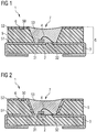
- FIG. 1 it is a light-emitting diode device 1 with a LED chip 2, which is mounted on an electrical connection conductor 31 of an electrical lead frame 3 (lead frame) and electrically connected via a rear side contact with this is.
- a front side contact of the LED chip 2 is connected by means of a bonding wire 4 with a second electrical connection conductor 32 of the electrical lead frame 3.
- the electrical connection conductors 31, 32 are formed by a first plastic component 51 of a plastic base body 5. In a reflector-like recess 7 on the front side 6 of the plastic base body 5, the mounting region for the LED chip 2 is formed.
- the electrical connecting conductors 31, 32 extend from the bottom surface of the recess 7 through the first plastic component 51 to the side surfaces thereof and protrude therefrom. Outside the plastic base body 5, the electrical connection conductors 31, 32 are bent toward the rear side thereof and further toward the rear side.
- the surface of the second plastic component 52 forms an optical functional area on the front side 6 of the plastic main body 5.
- it has, for example, at least one dye and / or at least one reflection-enhancing filler.
- a blackening of contrast increases the contrast.
- white filler such as titanium oxide, for example, the reflectivity of the front surface of the plastic base body 5 is increased.
- the second plastic component 52 covers the entire front 50 of the first plastic component 51 adjacent to the reflector-like Recess 7. In expedient embodiments (without representation), only a part of the front side 50 may be covered by the second plastic component.
- the second plastic component 52 is made of the same plastic base material as the first plastic component 51, for example of thermoplastic material or thermoset material.
- the plastic base material is, for example, a material based on epoxy resin or acrylic resin, but may also be any other material suitable for plastic base bodies of so-called premold designs.
- a window portion 53 which is made for example of a transparent or translucent plastic material, for example of a reaction resin such as epoxy resin or silicone resin.
- This window part encapsulates the LED chip 2 and is used inter alia to protect against adverse effects of environmental influences.
- the plastic base body 5, the window part 53 and the lead frame 3 together form the housing of the light-emitting diode component 1.
- the embodiment according to FIG. 2 differs from the according to FIG. 1 in particular in that the layer of the second plastic component 52 is drawn into the reflector-like recess 7, so that part of the lateral inner surface of the recess 7 is formed by a surface of the second plastic component 52.
- the materials of the embodiment according to FIG. 2 correspond for example those of the embodiment described above FIG. 1 ,
- Both embodiments of the housing described above are also applicable to photodiode devices.
- a photodiode chip is used instead of the light-emitting diode chip.
- a plastic base body 5 is produced by means of a two-component injection method (also called double-injection method).
- the first plastic component 51 is produced as a carrying part of the plastic base body.
- the second plastic component 51 which has the optical functional area of the plastic base body 5, is produced.
- the two plastic components 51, 52 differ, as explained in more detail in connection with the above embodiments, in at least one optical property of each other.
- the electrical connection conductors 31, 32 of the metallic lead frame 3 are encapsulated with the first plastic component 51 such that they extend from the mounting region for the light-emitting diode chip to the side surfaces of the plastic base body 5.
- the second plastic component 52 is formed on the front side of the first plastic component 51.
Landscapes
- Led Device Packages (AREA)
Applications Claiming Priority (2)
| Application Number | Priority Date | Filing Date | Title |
|---|---|---|---|
| DE102006046678A DE102006046678A1 (de) | 2006-09-29 | 2006-09-29 | Gehäuse für ein optoelektronisches Bauelement, optoelektronisches Bauelement und Verfahren zum Herstellen eines Gehäuses für ein optoelektronisches Bauelement |
| PCT/DE2007/001750 WO2008040324A1 (de) | 2006-09-29 | 2007-09-27 | Gehäuse für ein optoelektronisches bauelement, optoelektronisches bauelement und verfahren zum herstellen eines gehäuses für ein optoelektronisches bauelement |
Publications (2)
| Publication Number | Publication Date |
|---|---|
| EP2057695A1 EP2057695A1 (de) | 2009-05-13 |
| EP2057695B1 true EP2057695B1 (de) | 2018-08-15 |
Family
ID=38959635
Family Applications (1)
| Application Number | Title | Priority Date | Filing Date |
|---|---|---|---|
| EP07817592.4A Active EP2057695B1 (de) | 2006-09-29 | 2007-09-27 | Gehäuse für ein optoelektronisches bauelement, optoelektronisches bauelement und verfahren zum herstellen eines gehäuses für ein optoelektronisches bauelement |
Country Status (8)
Families Citing this family (23)
| Publication number | Priority date | Publication date | Assignee | Title |
|---|---|---|---|---|
| DE102009055786A1 (de) * | 2009-11-25 | 2011-05-26 | Osram Opto Semiconductors Gmbh | Gehäuse, optoelektronisches Bauteil und Verfahren zur Herstellung eines Gehäuses |
| DE102009058421A1 (de) * | 2009-12-16 | 2011-06-22 | OSRAM Opto Semiconductors GmbH, 93055 | Verfahren zur Herstellung eines Gehäuses für ein optoelektronisches Halbleiterbauteil, Gehäuse und optoelektronisches Halbleiterbauteil |
| DE102010011428A1 (de) | 2010-03-15 | 2011-09-15 | Osram Opto Semiconductors Gmbh | Optoelektronisches Bauelement und Verfahren zu dessen Herstellung |
| DE102010029368A1 (de) | 2010-05-27 | 2011-12-01 | Osram Opto Semiconductors Gmbh | Elektronische Anordnung und Verfahren zum Herstellen einer elektronischen Anordnung |
| DE102010023815A1 (de) | 2010-06-15 | 2011-12-15 | Osram Opto Semiconductors Gmbh | Oberflächenmontierbares optoelektronisches Bauelement und Verfahren zur Herstellung eines oberflächenmontierbaren optoelektronischen Bauelements |
| DE102010025319B4 (de) * | 2010-06-28 | 2022-05-25 | OSRAM Opto Semiconductors Gesellschaft mit beschränkter Haftung | Verfahren zur Herstellung eines oberflächenmontierbaren Halbleiterbauelements und oberflächenmontierbare Halbleiterbauelemente |
| JP5488310B2 (ja) * | 2010-07-30 | 2014-05-14 | 市光工業株式会社 | 車両用灯具の半導体型光源の光源ユニット、車両用灯具 |
| DE102010054591B4 (de) * | 2010-12-15 | 2023-03-30 | OSRAM Opto Semiconductors Gesellschaft mit beschränkter Haftung | Gehäuse und Verfahren zur Herstellung eines Gehäuses für ein optoelektronisches Bauelement |
| KR101825473B1 (ko) * | 2011-02-16 | 2018-02-05 | 삼성전자 주식회사 | 발광소자 패키지 및 그 제조방법 |
| CN103171080A (zh) * | 2011-12-21 | 2013-06-26 | 顺德工业股份有限公司 | 发光装置封装支架的制造方法 |
| US10134961B2 (en) * | 2012-03-30 | 2018-11-20 | Cree, Inc. | Submount based surface mount device (SMD) light emitter components and methods |
| US9735198B2 (en) | 2012-03-30 | 2017-08-15 | Cree, Inc. | Substrate based light emitter devices, components, and related methods |
| US10222032B2 (en) | 2012-03-30 | 2019-03-05 | Cree, Inc. | Light emitter components and methods having improved electrical contacts |
| CN102779926B (zh) * | 2012-08-02 | 2015-01-28 | 慧明光电(深圳)有限公司 | 高对比度的防水表贴led灯 |
| JP6392654B2 (ja) * | 2014-02-04 | 2018-09-19 | エイブリック株式会社 | 光センサ装置 |
| DE102014106882A1 (de) * | 2014-05-15 | 2015-11-19 | Osram Opto Semiconductors Gmbh | Optoelektronisches Bauelement |
| CN107251245A (zh) * | 2015-02-25 | 2017-10-13 | 京瓷株式会社 | 发光元件搭载用封装体、发光装置以及发光模块 |
| US9865779B2 (en) | 2015-09-30 | 2018-01-09 | Nichia Corporation | Methods of manufacturing the package and light-emitting device |
| JP6728764B2 (ja) * | 2016-02-26 | 2020-07-22 | 日亜化学工業株式会社 | 発光装置及びそれを用いた照明装置 |
| CN105575921A (zh) * | 2016-02-29 | 2016-05-11 | 卓广实业(上海)有限公司 | 垂直导热封装结构的ic元件 |
| US11511467B2 (en) * | 2017-09-19 | 2022-11-29 | Lumileds Llc | Light emitting device and manufacturing method thereof |
| JP6658808B2 (ja) * | 2017-12-25 | 2020-03-04 | 日亜化学工業株式会社 | 発光装置および発光装置の製造方法 |
| JP7212241B2 (ja) | 2018-06-21 | 2023-01-25 | 日亜化学工業株式会社 | 発光装置 |
Citations (1)
| Publication number | Priority date | Publication date | Assignee | Title |
|---|---|---|---|---|
| DE19945919A1 (de) * | 1998-09-25 | 2000-03-30 | Rohm Co Ltd | Licht ausstrahlende Halbleiter-Vorrichtung mit einem Reflektor |
Family Cites Families (23)
| Publication number | Priority date | Publication date | Assignee | Title |
|---|---|---|---|---|
| DE58909875D1 (de) * | 1989-05-31 | 2000-08-31 | Osram Opto Semiconductors Gmbh | Verfahren zum Montieren eines oberflächenmontierbaren Opto-Bauelements |
| US5291038A (en) * | 1990-12-19 | 1994-03-01 | Sharp Kabushiki Kaisha | Reflective type photointerrupter |
| JP2714272B2 (ja) * | 1991-06-04 | 1998-02-16 | シャープ株式会社 | 電子部品 |
| EP0646971B1 (de) * | 1993-09-30 | 1997-03-12 | Siemens Aktiengesellschaft | Zweipoliges SMT-Miniatur-Gehäuse für Halbleiterbauelemente und Verfahren zu dessen Herstellung |
| DE19638667C2 (de) | 1996-09-20 | 2001-05-17 | Osram Opto Semiconductors Gmbh | Mischfarbiges Licht abstrahlendes Halbleiterbauelement mit Lumineszenzkonversionselement |
| EP1004145B1 (de) * | 1997-07-29 | 2005-06-01 | Osram Opto Semiconductors GmbH | Optoelektronisches bauelement |
| DE19829197C2 (de) * | 1998-06-30 | 2002-06-20 | Siemens Ag | Strahlungsaussendendes und/oder -empfangendes Bauelement |
| DE10020465A1 (de) * | 2000-04-26 | 2001-11-08 | Osram Opto Semiconductors Gmbh | Strahlungsemittierendes Halbleiterbauelement mit Lumineszenzkonversionselement |
| JP4066620B2 (ja) * | 2000-07-21 | 2008-03-26 | 日亜化学工業株式会社 | 発光素子、および発光素子を配置した表示装置ならびに表示装置の製造方法 |
| DE10117889A1 (de) * | 2001-04-10 | 2002-10-24 | Osram Opto Semiconductors Gmbh | Leiterrahmen und Gehäuse für ein strahlungsemittierendes Bauelement, strahlungsemittierendes Bauelement sowie Verfahren zu dessen Herstellung |
| JP3844196B2 (ja) | 2001-06-12 | 2006-11-08 | シチズン電子株式会社 | 発光ダイオードの製造方法 |
| WO2003034508A1 (fr) * | 2001-10-12 | 2003-04-24 | Nichia Corporation | Dispositif d'emission de lumiere et procede de fabrication de celui-ci |
| DE10153259A1 (de) | 2001-10-31 | 2003-05-22 | Osram Opto Semiconductors Gmbh | Optoelektronisches Bauelement |
| EP1597764A1 (de) | 2003-02-28 | 2005-11-23 | Osram Opto Semiconductors GmbH | Optoelektronisches bauteil mit strukturiert metallisiertem gehäusekörper, verfahren zur herstellung eines derartigen bauteils und verfahren zur strukturierten metallisierung eines kunststoff enthaltenden körpers |
| TW200427111A (en) | 2003-03-12 | 2004-12-01 | Shinetsu Chemical Co | Material for coating/protecting light-emitting semiconductor and the light-emitting semiconductor device |
| EP1623823B1 (en) * | 2003-05-14 | 2014-07-02 | Toyo Seikan Group Holdings, Ltd. | Decorative plastic packaging body and method of recycling the same |
| JP4357886B2 (ja) | 2003-06-30 | 2009-11-04 | Tdk株式会社 | 脱バインダ用治具および電子部品の製造方法 |
| US20050196710A1 (en) * | 2004-03-04 | 2005-09-08 | Semiconductor Energy Laboratory Co., Ltd. | Method for forming pattern, thin film transistor, display device and method for manufacturing the same, and television apparatus |
| JP4747726B2 (ja) * | 2004-09-09 | 2011-08-17 | 豊田合成株式会社 | 発光装置 |
| DE102004045950A1 (de) * | 2004-09-22 | 2006-03-30 | Osram Opto Semiconductors Gmbh | Gehäuse für ein optoelektronisches Bauelement, optoelektronisches Bauelement und Verfahren zur Herstellung eines optoelektronischen Bauelements |
| JP2006186297A (ja) | 2004-12-03 | 2006-07-13 | Toshiba Corp | 半導体発光装置及びその製造方法 |
| US7932499B2 (en) * | 2006-03-13 | 2011-04-26 | Hitachi Metals, Ltd. | Radiation detector and method for producing the same |
| US9502624B2 (en) * | 2006-05-18 | 2016-11-22 | Nichia Corporation | Resin molding, surface mounted light emitting apparatus and methods for manufacturing the same |
-
2006
- 2006-09-29 DE DE102006046678A patent/DE102006046678A1/de not_active Withdrawn
-
2007
- 2007-09-19 TW TW096134770A patent/TWI347679B/zh active
- 2007-09-27 JP JP2009529530A patent/JP5340157B2/ja active Active
- 2007-09-27 EP EP07817592.4A patent/EP2057695B1/de active Active
- 2007-09-27 US US12/443,160 patent/US8071987B2/en active Active
- 2007-09-27 CN CN2007800362142A patent/CN101523621B/zh active Active
- 2007-09-27 KR KR1020097006101A patent/KR101444479B1/ko active Active
- 2007-09-27 WO PCT/DE2007/001750 patent/WO2008040324A1/de active Application Filing
-
2011
- 2011-10-18 US US13/275,980 patent/US8476114B2/en not_active Expired - Fee Related
Patent Citations (1)
| Publication number | Priority date | Publication date | Assignee | Title |
|---|---|---|---|---|
| DE19945919A1 (de) * | 1998-09-25 | 2000-03-30 | Rohm Co Ltd | Licht ausstrahlende Halbleiter-Vorrichtung mit einem Reflektor |
Also Published As
| Publication number | Publication date |
|---|---|
| TW200830560A (en) | 2008-07-16 |
| US20120032362A1 (en) | 2012-02-09 |
| US8071987B2 (en) | 2011-12-06 |
| CN101523621A (zh) | 2009-09-02 |
| EP2057695A1 (de) | 2009-05-13 |
| US20090218584A1 (en) | 2009-09-03 |
| DE102006046678A1 (de) | 2008-04-03 |
| JP2010505254A (ja) | 2010-02-18 |
| JP5340157B2 (ja) | 2013-11-13 |
| KR101444479B1 (ko) | 2014-09-25 |
| WO2008040324A1 (de) | 2008-04-10 |
| KR20090075806A (ko) | 2009-07-09 |
| TWI347679B (en) | 2011-08-21 |
| CN101523621B (zh) | 2012-01-18 |
| US8476114B2 (en) | 2013-07-02 |
Similar Documents
| Publication | Publication Date | Title |
|---|---|---|
| EP2057695B1 (de) | Gehäuse für ein optoelektronisches bauelement, optoelektronisches bauelement und verfahren zum herstellen eines gehäuses für ein optoelektronisches bauelement | |
| DE19829197C2 (de) | Strahlungsaussendendes und/oder -empfangendes Bauelement | |
| EP2215657B1 (de) | Anordnung mit mindestens zwei lichtemittierenden halbleiterbauelementen und herstellungsverfahren dafür | |
| DE19918370B4 (de) | LED-Weißlichtquelle mit Linse | |
| EP2126989A1 (de) | Optoelektronische vorrichtung mit gehäusekörper | |
| DE102007001706A1 (de) | Gehäuse für optoelektronisches Bauelement und Anordnung eines optoelektronischen Bauelementes in einem Gehäuse | |
| DE102010021791A1 (de) | Optoelektronisches Bauelement und Verfahren zur Herstellung eines optoelektronischen Bauelements und eines Verbunds | |
| EP1700349B1 (de) | Verfahren zum herstellen einer mehrzahl strahlungsemittierender und/oder strahlungsempfangender halbleiterbauelemente | |
| DE102007029369A1 (de) | Optoelektronisches Halbleiterbauelement und Verfahren zur Herstellung eines optoelektronischen Halbleiterbauelements | |
| DE19536738A1 (de) | Halbleiterschaltung mit Betriebsanzeige | |
| DE102007017335A1 (de) | Beleuchtungseinheit mit einer transparenten Trägerplatte und daraufsitzender Leuchtdiode | |
| DE102012101102A1 (de) | Optoelektronisches Halbleiterbauelement und Anordnung mit einer Mehrzahl von derartigen Bauelementen | |
| EP1717871A2 (de) | Oberflächenmontierbares optoelektronisches Bauelement | |
| EP1627455B1 (de) | Gehäuse für ein laserdiodenbauelement und laserdiodenbauelement | |
| DE69034090T2 (de) | Halbleitervorrichtung zur Detektion oder Emission von Magnetfeldlinien oder Licht | |
| DE102014113844B4 (de) | Verfahren zum Herstellen eines optoelektronischen Bauelements und optoelektronisches Bauelement | |
| DE212013000297U1 (de) | Optoelektronisches Bauelement | |
| DE202004005228U1 (de) | Strahlungsemittierendes und/oder strahlungsempfangendes Halbleiterbauelement | |
| DE102004047640A1 (de) | Optoelektronisches Bauelement und Gehäuse für ein optoelektronisches Bauelement | |
| DE102008003971A1 (de) | Leuchtdiodenanordnung mit Schutzrahmen | |
| DE112019001007B4 (de) | Verfahren zum Herstellen eines optoelektronischen Bauelements | |
| EP2329477A1 (de) | Optoelektronisches bauteil | |
| DE102013207111B4 (de) | Optoelektronisches Bauelement | |
| WO2021224015A1 (de) | Optoelektronisches bauelment und verfahren zu dessen herstellung | |
| DE102014117435A1 (de) | Bauteil mit Leiterrahmenabschnitt |
Legal Events
| Date | Code | Title | Description |
|---|---|---|---|
| PUAI | Public reference made under article 153(3) epc to a published international application that has entered the european phase |
Free format text: ORIGINAL CODE: 0009012 |
|
| 17P | Request for examination filed |
Effective date: 20090325 |
|
| AK | Designated contracting states |
Kind code of ref document: A1 Designated state(s): AT BE BG CH CY CZ DE DK EE ES FI FR GB GR HU IE IS IT LI LT LU LV MC MT NL PL PT RO SE SI SK TR |
|
| AX | Request for extension of the european patent |
Extension state: AL BA HR MK RS |
|
| DAX | Request for extension of the european patent (deleted) | ||
| RBV | Designated contracting states (corrected) |
Designated state(s): DE FR GB |
|
| 17Q | First examination report despatched |
Effective date: 20150511 |
|
| GRAP | Despatch of communication of intention to grant a patent |
Free format text: ORIGINAL CODE: EPIDOSNIGR1 |
|
| INTG | Intention to grant announced |
Effective date: 20180319 |
|
| GRAS | Grant fee paid |
Free format text: ORIGINAL CODE: EPIDOSNIGR3 |
|
| GRAA | (expected) grant |
Free format text: ORIGINAL CODE: 0009210 |
|
| AK | Designated contracting states |
Kind code of ref document: B1 Designated state(s): DE FR GB |
|
| REG | Reference to a national code |
Ref country code: GB Ref legal event code: FG4D Free format text: NOT ENGLISH |
|
| REG | Reference to a national code |
Ref country code: DE Ref legal event code: R096 Ref document number: 502007016338 Country of ref document: DE |
|
| REG | Reference to a national code |
Ref country code: DE Ref legal event code: R097 Ref document number: 502007016338 Country of ref document: DE |
|
| PLBE | No opposition filed within time limit |
Free format text: ORIGINAL CODE: 0009261 |
|
| STAA | Information on the status of an ep patent application or granted ep patent |
Free format text: STATUS: NO OPPOSITION FILED WITHIN TIME LIMIT |
|
| 26N | No opposition filed |
Effective date: 20190516 |
|
| GBPC | Gb: european patent ceased through non-payment of renewal fee |
Effective date: 20181115 |
|
| PG25 | Lapsed in a contracting state [announced via postgrant information from national office to epo] |
Ref country code: FR Free format text: LAPSE BECAUSE OF NON-PAYMENT OF DUE FEES Effective date: 20181015 |
|
| PG25 | Lapsed in a contracting state [announced via postgrant information from national office to epo] |
Ref country code: GB Free format text: LAPSE BECAUSE OF NON-PAYMENT OF DUE FEES Effective date: 20181115 |
|
| P01 | Opt-out of the competence of the unified patent court (upc) registered |
Effective date: 20230825 |
|
| PGFP | Annual fee paid to national office [announced via postgrant information from national office to epo] |
Ref country code: DE Payment date: 20240918 Year of fee payment: 18 |
|
| REG | Reference to a national code |
Ref country code: DE Ref legal event code: R079 Ref document number: 502007016338 Country of ref document: DE Free format text: PREVIOUS MAIN CLASS: H01L0033000000 Ipc: H10H0020000000 |