EP2057695B1 - Housing for an optoelectronic component, optoelectronic component and method for producing a housing for an optoelectronic component - Google Patents
Housing for an optoelectronic component, optoelectronic component and method for producing a housing for an optoelectronic component Download PDFInfo
- Publication number
- EP2057695B1 EP2057695B1 EP07817592.4A EP07817592A EP2057695B1 EP 2057695 B1 EP2057695 B1 EP 2057695B1 EP 07817592 A EP07817592 A EP 07817592A EP 2057695 B1 EP2057695 B1 EP 2057695B1
- Authority
- EP
- European Patent Office
- Prior art keywords
- plastic
- base body
- component
- plastic base
- plastic component
- Prior art date
- Legal status (The legal status is an assumption and is not a legal conclusion. Google has not performed a legal analysis and makes no representation as to the accuracy of the status listed.)
- Active
Links
- 230000005693 optoelectronics Effects 0.000 title claims description 10
- 238000004519 manufacturing process Methods 0.000 title claims description 6
- 239000004033 plastic Substances 0.000 claims description 126
- 229920003023 plastic Polymers 0.000 claims description 126
- 239000000463 material Substances 0.000 claims description 32
- 238000000034 method Methods 0.000 claims description 17
- 230000003287 optical effect Effects 0.000 claims description 16
- 238000002310 reflectometry Methods 0.000 claims description 6
- 238000002347 injection Methods 0.000 claims description 5
- 239000007924 injection Substances 0.000 claims description 5
- 230000005855 radiation Effects 0.000 claims 4
- 239000000049 pigment Substances 0.000 claims 2
- 239000004638 Duroplast Substances 0.000 claims 1
- 229920000965 Duroplast Polymers 0.000 claims 1
- 239000003086 colorant Substances 0.000 claims 1
- 239000002184 metal Substances 0.000 claims 1
- 239000004020 conductor Substances 0.000 description 14
- 239000004065 semiconductor Substances 0.000 description 7
- 239000000945 filler Substances 0.000 description 6
- 239000012815 thermoplastic material Substances 0.000 description 5
- 229920001187 thermosetting polymer Polymers 0.000 description 4
- 238000011161 development Methods 0.000 description 2
- 230000018109 developmental process Effects 0.000 description 2
- 230000007613 environmental effect Effects 0.000 description 2
- 239000003822 epoxy resin Substances 0.000 description 2
- WABPQHHGFIMREM-UHFFFAOYSA-N lead(0) Chemical compound [Pb] WABPQHHGFIMREM-UHFFFAOYSA-N 0.000 description 2
- 229920000647 polyepoxide Polymers 0.000 description 2
- 238000001721 transfer moulding Methods 0.000 description 2
- 239000004925 Acrylic resin Substances 0.000 description 1
- 229920000178 Acrylic resin Polymers 0.000 description 1
- GWEVSGVZZGPLCZ-UHFFFAOYSA-N Titan oxide Chemical compound O=[Ti]=O GWEVSGVZZGPLCZ-UHFFFAOYSA-N 0.000 description 1
- 230000002411 adverse Effects 0.000 description 1
- 238000013459 approach Methods 0.000 description 1
- 238000004040 coloring Methods 0.000 description 1
- 230000000694 effects Effects 0.000 description 1
- 230000005670 electromagnetic radiation Effects 0.000 description 1
- 238000004299 exfoliation Methods 0.000 description 1
- 238000001746 injection moulding Methods 0.000 description 1
- 229920005989 resin Polymers 0.000 description 1
- 239000011347 resin Substances 0.000 description 1
- 229920002050 silicone resin Polymers 0.000 description 1
- 238000005507 spraying Methods 0.000 description 1
- OGIDPMRJRNCKJF-UHFFFAOYSA-N titanium oxide Inorganic materials [Ti]=O OGIDPMRJRNCKJF-UHFFFAOYSA-N 0.000 description 1
Images
Classifications
-
- H—ELECTRICITY
- H01—ELECTRIC ELEMENTS
- H01L—SEMICONDUCTOR DEVICES NOT COVERED BY CLASS H10
- H01L31/00—Semiconductor devices sensitive to infrared radiation, light, electromagnetic radiation of shorter wavelength or corpuscular radiation and specially adapted either for the conversion of the energy of such radiation into electrical energy or for the control of electrical energy by such radiation; Processes or apparatus specially adapted for the manufacture or treatment thereof or of parts thereof; Details thereof
- H01L31/02—Details
- H01L31/0203—Containers; Encapsulations, e.g. encapsulation of photodiodes
-
- H—ELECTRICITY
- H01—ELECTRIC ELEMENTS
- H01L—SEMICONDUCTOR DEVICES NOT COVERED BY CLASS H10
- H01L33/00—Semiconductor devices with at least one potential-jump barrier or surface barrier specially adapted for light emission; Processes or apparatus specially adapted for the manufacture or treatment thereof or of parts thereof; Details thereof
- H01L33/44—Semiconductor devices with at least one potential-jump barrier or surface barrier specially adapted for light emission; Processes or apparatus specially adapted for the manufacture or treatment thereof or of parts thereof; Details thereof characterised by the coatings, e.g. passivation layer or anti-reflective coating
-
- H—ELECTRICITY
- H01—ELECTRIC ELEMENTS
- H01L—SEMICONDUCTOR DEVICES NOT COVERED BY CLASS H10
- H01L33/00—Semiconductor devices with at least one potential-jump barrier or surface barrier specially adapted for light emission; Processes or apparatus specially adapted for the manufacture or treatment thereof or of parts thereof; Details thereof
- H01L33/48—Semiconductor devices with at least one potential-jump barrier or surface barrier specially adapted for light emission; Processes or apparatus specially adapted for the manufacture or treatment thereof or of parts thereof; Details thereof characterised by the semiconductor body packages
- H01L33/58—Optical field-shaping elements
- H01L33/60—Reflective elements
-
- H—ELECTRICITY
- H01—ELECTRIC ELEMENTS
- H01L—SEMICONDUCTOR DEVICES NOT COVERED BY CLASS H10
- H01L2224/00—Indexing scheme for arrangements for connecting or disconnecting semiconductor or solid-state bodies and methods related thereto as covered by H01L24/00
- H01L2224/01—Means for bonding being attached to, or being formed on, the surface to be connected, e.g. chip-to-package, die-attach, "first-level" interconnects; Manufacturing methods related thereto
- H01L2224/42—Wire connectors; Manufacturing methods related thereto
- H01L2224/47—Structure, shape, material or disposition of the wire connectors after the connecting process
- H01L2224/48—Structure, shape, material or disposition of the wire connectors after the connecting process of an individual wire connector
- H01L2224/481—Disposition
- H01L2224/48151—Connecting between a semiconductor or solid-state body and an item not being a semiconductor or solid-state body, e.g. chip-to-substrate, chip-to-passive
- H01L2224/48221—Connecting between a semiconductor or solid-state body and an item not being a semiconductor or solid-state body, e.g. chip-to-substrate, chip-to-passive the body and the item being stacked
- H01L2224/48245—Connecting between a semiconductor or solid-state body and an item not being a semiconductor or solid-state body, e.g. chip-to-substrate, chip-to-passive the body and the item being stacked the item being metallic
- H01L2224/48247—Connecting between a semiconductor or solid-state body and an item not being a semiconductor or solid-state body, e.g. chip-to-substrate, chip-to-passive the body and the item being stacked the item being metallic connecting the wire to a bond pad of the item
-
- H—ELECTRICITY
- H01—ELECTRIC ELEMENTS
- H01L—SEMICONDUCTOR DEVICES NOT COVERED BY CLASS H10
- H01L31/00—Semiconductor devices sensitive to infrared radiation, light, electromagnetic radiation of shorter wavelength or corpuscular radiation and specially adapted either for the conversion of the energy of such radiation into electrical energy or for the control of electrical energy by such radiation; Processes or apparatus specially adapted for the manufacture or treatment thereof or of parts thereof; Details thereof
- H01L31/02—Details
- H01L31/0232—Optical elements or arrangements associated with the device
-
- H—ELECTRICITY
- H01—ELECTRIC ELEMENTS
- H01L—SEMICONDUCTOR DEVICES NOT COVERED BY CLASS H10
- H01L33/00—Semiconductor devices with at least one potential-jump barrier or surface barrier specially adapted for light emission; Processes or apparatus specially adapted for the manufacture or treatment thereof or of parts thereof; Details thereof
- H01L33/48—Semiconductor devices with at least one potential-jump barrier or surface barrier specially adapted for light emission; Processes or apparatus specially adapted for the manufacture or treatment thereof or of parts thereof; Details thereof characterised by the semiconductor body packages
- H01L33/483—Containers
- H01L33/486—Containers adapted for surface mounting
Definitions
- the invention relates to a housing for an optoelectronic component, in particular a surface-mountable optoelectronic component, having a plastic base body which has a front side with a mounting region for at least one radiation-emitting or radiation-detecting body. It further relates to a particular surface-mountable optoelectronic component and to a method for producing a housing for an optoelectronic component.
- Housing of the type mentioned are, for example, in the publications EP 1022787 B1 .
- An object of the present invention is to provide a housing of the type mentioned, with the desired optical properties of the housing surface can be achieved in an improved manner. Furthermore, a method for producing such a housing is to be specified.
- the plastic base body is formed from at least one first plastic component and at least one second plastic component.
- the second plastic component is located on the front side of the plastic base body and is formed of a material that differs in at least one optical property of the material of the first plastic component.
- the surface of the second plastic component forms, for example, caused by the addition of dye or reflection-increasing filler, an optical functional area of the plastic base body.
- black dye an increase in contrast can be achieved.
- white filler advantageously, the reflectivity of the front surface of the plastic base body can be increased.
- the plastic base body encloses electrical connection conductors of a metallic lead frame, such that they extend from the mounting area to the surface of the plastic base body.
- the mounting area is arranged in a reflector-like depression of the plastic base body.
- the second plastic component forms a layer along the entire front side or along a partial region of the front side of the plastic main body except for the reflector-like depression. In another advantageous embodiment, this layer is additionally pulled along at least a portion of the lateral inner surfaces in the reflector-like depression.
- the thickness of the layer is advantageously between 50 ⁇ m inclusive and 100 ⁇ m inclusive.
- the second plastic component of the same plastic base material made like the first plastic component.
- a plastic base material is preferably thermoplastic material or thermoset material.
- a plastic base body is produced by means of a two-component injection method (also called double-injection method).
- a supporting part of the plastic base body is preferably produced from a first plastic component and, in a further step, an optical functional area of the plastic base body is produced from a second plastic component.
- the two plastic components differ from each other in at least one optical property. In an alternative method, these two steps are performed in reverse order.
- the term "spraying method” covers both injection molding methods and transfer molding methods, as well as transfer molding methods.
- a dye is mixed into the second plastic component, for example, which gives it a different color from the first plastic component.
- a black coloring is suitable.
- the second plastic component is filled with a reflection-increasing material.
- electrical connecting conductors of a metallic leadframe are encapsulated with the first plastic component such that they extend from the mounting region for at least one radiation-emitting or radiation-detecting body to the surface of the plastic main body.
- the second plastic component is formed on the first plastic component.
- a reflector-like depression is preferably formed, in which the mounting region for the semiconductor body is located.
- the optical functional area is made of the same plastic base material as the rest of the plastic base body.
- a plastic base material is, as already stated above, preferably thermoplastic material or thermoset material.
- At least one semiconductor body which is suitable for emitting and / or detecting electromagnetic radiation (for example a light-emitting diode or laser duplex chip or a photodiode chip) is fastened in a plastic base body.
- the plastic base body has on its front side a mounting region for the semiconductor body, which is surrounded by a translucent window part and encapsulates the semiconductor body.
- Electrical connection conductors run from the mounting area to the outer surface of the plastic base body.
- the semiconductor body is preferably arranged on one of the electrical connection conductors.
- Electrical connection surfaces of the semiconductor body are electrically conductively connected to the electrical connection conductors, for example, on the one hand by means of an electrical connection layer between a rear connection surface and the an electrical connection conductor and on the other hand by means of a bonding wire between a front-side pad and a second electrical connection conductor.
- the semiconductor body can, however, also be connected to the connection conductors by other means by means of suitable electrical connection means.
- an optical functional area is formed of a material whose optical properties are different from those of the remaining material of the plastic base body.
- the optical functional area is formed by a free surface of a separate plastic component of the plastic base body, for example, caused by the addition of dye or reflection-enhancing filler to the separate plastic component.
- a separate plastic component of the plastic base body for example, caused by the addition of dye or reflection-enhancing filler to the separate plastic component.
- black dye an increase in contrast can be achieved.
- white filler advantageously, the reflectivity of the front side of the plastic base body can be increased.
- the mounting area is advantageously arranged in a reflector-like depression of the plastic base body.
- the separate plastic component of the same plastic base material is made as the plastic component (s), which forms the other plastic base body (form).
- a plastic base material is preferably thermoplastic material or thermoset material.
- the separate plastic component forms a layer along the entire front side or along a partial region of the front side of the plastic main body except for the reflector-like depression.
- this layer is additionally drawn along at least a portion of the lateral inner surfaces in the reflector-like depression.
- the thickness of the layer is preferably between 50 ⁇ m and 100 ⁇ m inclusive.
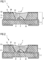
- FIG. 1 it is a light-emitting diode device 1 with a LED chip 2, which is mounted on an electrical connection conductor 31 of an electrical lead frame 3 (lead frame) and electrically connected via a rear side contact with this is.
- a front side contact of the LED chip 2 is connected by means of a bonding wire 4 with a second electrical connection conductor 32 of the electrical lead frame 3.
- the electrical connection conductors 31, 32 are formed by a first plastic component 51 of a plastic base body 5. In a reflector-like recess 7 on the front side 6 of the plastic base body 5, the mounting region for the LED chip 2 is formed.
- the electrical connecting conductors 31, 32 extend from the bottom surface of the recess 7 through the first plastic component 51 to the side surfaces thereof and protrude therefrom. Outside the plastic base body 5, the electrical connection conductors 31, 32 are bent toward the rear side thereof and further toward the rear side.
- the surface of the second plastic component 52 forms an optical functional area on the front side 6 of the plastic main body 5.
- it has, for example, at least one dye and / or at least one reflection-enhancing filler.
- a blackening of contrast increases the contrast.
- white filler such as titanium oxide, for example, the reflectivity of the front surface of the plastic base body 5 is increased.
- the second plastic component 52 covers the entire front 50 of the first plastic component 51 adjacent to the reflector-like Recess 7. In expedient embodiments (without representation), only a part of the front side 50 may be covered by the second plastic component.
- the second plastic component 52 is made of the same plastic base material as the first plastic component 51, for example of thermoplastic material or thermoset material.
- the plastic base material is, for example, a material based on epoxy resin or acrylic resin, but may also be any other material suitable for plastic base bodies of so-called premold designs.
- a window portion 53 which is made for example of a transparent or translucent plastic material, for example of a reaction resin such as epoxy resin or silicone resin.
- This window part encapsulates the LED chip 2 and is used inter alia to protect against adverse effects of environmental influences.
- the plastic base body 5, the window part 53 and the lead frame 3 together form the housing of the light-emitting diode component 1.
- the embodiment according to FIG. 2 differs from the according to FIG. 1 in particular in that the layer of the second plastic component 52 is drawn into the reflector-like recess 7, so that part of the lateral inner surface of the recess 7 is formed by a surface of the second plastic component 52.
- the materials of the embodiment according to FIG. 2 correspond for example those of the embodiment described above FIG. 1 ,
- Both embodiments of the housing described above are also applicable to photodiode devices.
- a photodiode chip is used instead of the light-emitting diode chip.
- a plastic base body 5 is produced by means of a two-component injection method (also called double-injection method).
- the first plastic component 51 is produced as a carrying part of the plastic base body.
- the second plastic component 51 which has the optical functional area of the plastic base body 5, is produced.
- the two plastic components 51, 52 differ, as explained in more detail in connection with the above embodiments, in at least one optical property of each other.
- the electrical connection conductors 31, 32 of the metallic lead frame 3 are encapsulated with the first plastic component 51 such that they extend from the mounting region for the light-emitting diode chip to the side surfaces of the plastic base body 5.
- the second plastic component 52 is formed on the front side of the first plastic component 51.
Description
Die Erfindung betrifft ein Gehäuse für ein optoelektronisches Bauelement, insbesondere ein oberflächenmontierbares optoelektronisches Bauelement, mit einem Kunststoff-Grundkörper, der eine Vorderseite mit einem Montagebereich für mindestens einen strahlungsemittierenden oder strahlungsdetektierenden Körper aufweist. Sie betrifft weiterhin ein insbesondere oberflächenmontierbares optoelektronisches Bauelement und ein Verfahren zum Herstellen eines Gehäuses für ein optoelektronisches Bauelement.
Gehäuse der eingangs genannten Art sind beispielsweise in den Druckschriften
Diese bekannten Kunststoff-Grundkörper weisen aber für eine Reihe von Anwendungen nicht hinreichend zufriedenstellende optische Eigenschaften auf. So ist beispielsweise für die Anwendung bei Video-Displays der Kontrast der Leuchtpunkte zur umgebenden Gehäuseoberfläche oftmals zu gering.
Ein Ansatz, diesem Problem zu begegnen, besteht darin, die Oberfläche des Kuntststoff-Grundkörpers nachträglich beispielsweise mit schwarzer Farbe zu bedrucken (siehe zum Beispiel
Diese Aufgaben werden durch ein Gehäuse mit den Merkmalen des Anspruches 1 bzw. durch ein Verfahren mit den Merkmalen des Patentanspruches 8 gelöst.The invention relates to a housing for an optoelectronic component, in particular a surface-mountable optoelectronic component, having a plastic base body which has a front side with a mounting region for at least one radiation-emitting or radiation-detecting body. It further relates to a particular surface-mountable optoelectronic component and to a method for producing a housing for an optoelectronic component.
Housing of the type mentioned are, for example, in the publications
However, these known plastic base bodies do not have sufficiently satisfactory optical properties for a number of applications. For example, for the application For video displays, the contrast of the luminous dots to the surrounding housing surface is often too low.
One approach to countering this problem is to subsequently print the surface of the Kuntststoff base body, for example, with black ink (see, for example
These objects are achieved by a housing having the features of claim 1 or by a method having the features of claim 8.
Vorteilhafte Ausgestaltungen und Weiterbildungen des Gehäuses, des Bauelements und des Verfahrens sind in den Unteransprüchen angegeben.
Der Offenbarungsgehalt der Ansprüche wird hiermit ausdrücklich durch Rückbezug in die Beschreibung aufgenommen.
Bei einem Gehäuse gemäß der Erfindung ist der Kunststoff-Grundkörper aus mindestens einer ersten Kunststoffkomponente und mindestens einer zweiten Kunststoffkomponente ausgebildet. Die zweite Kunststoffkomponente befindet sich dabei an der Vorderseite des Kunststoff-Grundkörpers und ist aus einem Material ausgebildet ist, das sich in mindestens einer optischen Eigenschaft von dem Material der ersten Kunststoffkomponente unterscheidet. Die Oberfläche der zweiten Kunststoffkomponente bildet, beispielsweise hervorgerufen durch Zugabe von Farbstoff oder reflexionssteigerndem Füllstoff, einen optischen Funktionsbereich des Kunststoff-Grundkörpers aus. So kann vorteilhafterweise durch Zugabe von schwarzem Farbstoff eine Kontrasterhöhung erzielt werden. Durch Zugabe von weißem Füllstoff kann vorteilhafterweise die Reflektivität der vorderseitigen Oberfläche des Kunststoff-Grundkörpers erhöht werden.Advantageous embodiments and further developments of the housing, the component and the method are specified in the subclaims.
The disclosure of the claims is hereby expressly incorporated by reference into the description.
In a housing according to the invention, the plastic base body is formed from at least one first plastic component and at least one second plastic component. The second plastic component is located on the front side of the plastic base body and is formed of a material that differs in at least one optical property of the material of the first plastic component. The surface of the second plastic component forms, for example, caused by the addition of dye or reflection-increasing filler, an optical functional area of the plastic base body. Thus, advantageously by adding black dye, an increase in contrast can be achieved. By adding white filler, advantageously, the reflectivity of the front surface of the plastic base body can be increased.
Bei einer vorteilhaften Ausgestaltung umschließt der Kunststoff-Grundkörper elektrische Anschlussleiter eines metallischen Leadframes, derart, dass diese vom Montagebereich zur Oberfläche des Kunststoff-Grundkörpers verlaufen. Der Montagebereich ist dabei in einer reflektorartigen Vertiefung des Kunststoff-Grundkörpers angeordnet. Die zweite Kunststoffkomponente bildet entlang der gesamten Vorderseite oder entlang eines Teilbereiches der Vorderseite des Kunststoff-Grundkörpers bis auf die reflektorartige Vertiefung eine Schicht aus. Bei einer anderen vorteilhaften Ausgestaltung ist diese Schicht zusätzlich auch entlang zumindest eines Teilbereiches der seitlichen Innenflächen in die reflektorartige Vertiefung gezogen.In an advantageous embodiment of the plastic base body encloses electrical connection conductors of a metallic lead frame, such that they extend from the mounting area to the surface of the plastic base body. The mounting area is arranged in a reflector-like depression of the plastic base body. The second plastic component forms a layer along the entire front side or along a partial region of the front side of the plastic main body except for the reflector-like depression. In another advantageous embodiment, this layer is additionally pulled along at least a portion of the lateral inner surfaces in the reflector-like depression.
Die Dicke der Schicht liegt vorteilhafterweise zwischen einschließlich 50 µm und einschließlich 100 µm.The thickness of the layer is advantageously between 50 μm inclusive and 100 μm inclusive.
Bei einer weiteren vorteilhaften Ausgestaltung ist die zweite Kunststoffkomponente aus dem gleichen Kunststoff-Grundmaterial gefertigt wie die erste Kunststoffkomponente. Als Kunststoff-Grundmaterial eignet sich vorzugsweise Thermoplast-Material oder Duroplast-Material.In a further advantageous embodiment, the second plastic component of the same plastic base material made like the first plastic component. As a plastic base material is preferably thermoplastic material or thermoset material.
Bei einem Verfahren gemäß der Erfindung wird mittels eines Zweikomponenten-Spritzverfahrens (auch Doppelspritzverfahren genannt) ein Kunststoff-Grundkörper hergestellt. Bevorzugt wird in einem ersten Schritt dabei ein tragender Teil des Kunststoff-Grundkörpers aus einer ersten Kunststoffkomponente hergestellt und in einem weiteren Schritt ein optischer Funktionsbereich des Kunststoff-Grundkörpers aus einer zweiten Kunststoffkomponente hergestellt. Die beiden Kunststoffkomponenten unterscheiden sich in mindestens einer optischen Eigenschaft voneinander. Bei einem alternativen Verfahren werden diese beiden Schritte in umgekehrter Reihenfolge ausgeführt.In a method according to the invention, a plastic base body is produced by means of a two-component injection method (also called double-injection method). In a first step, a supporting part of the plastic base body is preferably produced from a first plastic component and, in a further step, an optical functional area of the plastic base body is produced from a second plastic component. The two plastic components differ from each other in at least one optical property. In an alternative method, these two steps are performed in reverse order.
Vorliegend und im Rahmen der Beschreibung der Ausführungsbeispiele fallen unter den Begriff "Spritzverfahren" sowohl Spritzgussverfahren und Spritzpressverfahren, wie auch Transfermoldverfahren.In the present context and within the scope of the description of the exemplary embodiments, the term "spraying method" covers both injection molding methods and transfer molding methods, as well as transfer molding methods.
Bei einem Verfahren zum Herstellen eines Gehäuses mit verbessertem Kontrast wird in die zweite Kunststoffkomponente beispielsweise ein Farbstoff eingemischt, der diesem eine gegenüber der ersten Kunststoffkomponente verschiedene Farbe verleiht. Hierzu eignet sich vorzugsweise eine schwarze Einfärbung. Um beispielsweise die Reflektivität der Gehäuse-Vorderseite zu verbessern wird bei einer anderen Ausführungsform die zweite Kunststoffkomponente mit einem reflexionssteigerenden Material gefüllt.In a method for producing a housing with improved contrast, a dye is mixed into the second plastic component, for example, which gives it a different color from the first plastic component. For this purpose, preferably a black coloring is suitable. In order to improve, for example, the reflectivity of the housing front side, in another embodiment, the second plastic component is filled with a reflection-increasing material.
Bei einer besonders vorteilhaften Ausgestaltung des Verfahrens werden elektrische Anschlussleiter eines metallischen Leiterrahmens mit der ersten Kunststoffkomponente derart umspritzt, dass diese vom Montagebereich für mindestens einen strahlungsemittierenden oder strahlungsdetektierenden Körper zur Oberfläche des Kunststoff-Grundkörpers verlaufen. Nachfolgend wird in einem weiteren Schritt die zweite Kunststoffkomponente an der ersten Kunststoffkomponente ausgebildet. In der ersten Kunststoffkomponente des Kunststoff-Grundkörpers wird dabei vorzugsweise eine reflektorartige Vertiefung ausgebildet, in der sich der Montagebereich für den Halbleiterkörper befindet. Weiterhin vorzugsweise wird der optische Funktionsbereich aus dem gleichen Kunststoff-Grundmaterial gefertigt, wie der übrige Kunststoff-Grundkörper. Als Kunststoff-Grundmaterial eignet sich, wie oben bereits angegeben, vorzugsweise Thermoplast-Material oder Duroplast-Material.In a particularly advantageous embodiment of the method, electrical connecting conductors of a metallic leadframe are encapsulated with the first plastic component such that they extend from the mounting region for at least one radiation-emitting or radiation-detecting body to the surface of the plastic main body. Subsequently, in a further step, the second plastic component is formed on the first plastic component. In the first plastic component of the plastic base body, a reflector-like depression is preferably formed, in which the mounting region for the semiconductor body is located. Furthermore, preferably, the optical functional area is made of the same plastic base material as the rest of the plastic base body. As a plastic base material is, as already stated above, preferably thermoplastic material or thermoset material.
Bei einem optoelektronischen Bauelement gemäß der Erfindung ist mindestens ein Halbleiterkörper, der geeignet ist, elektromagnetische Strahlung auszusenden und/oder zu detektieren (beispielsweise ein Leuchtdioden- oder Laserdidoenchip oder ein Photodiodenchip), in einem Kunststoff-Grundkörper befestigt. Der Kunststoff-Grundkörper weist an seiner Vorderseite einen Montagebereich für den Halbleiterkörper auf, der von einem lichtdurchlässigen Fensterteil umgeben ist und den Halbleiterkörper verkapselt. Elektrische Anschlussleiter verlaufen vom Montagebereich zur äußeren Oberfläche des Kunststoff-Grundkörpers. Der Halbleiterkörper ist bevorzugt auf einem der elektrischen Anschlussleiter angeordnet. Elektrische Anschlussflächen des Halbleiterkörpers sind elektrisch leitend mit den elektrischen Anschlussleitern verbunden, beispielsweise einerseits mittels einer elektrischen Anschlussschicht zwischen einer rückseitigen Anschlussfläche und dem einen elektrischen Anschlussleiter und andererseits mittels eines Bonddrahtes zwischen einer vorderseitigen Anschlussfläche und einem zweiten elektrischen Anschlussleiter. Der Halbleiterkörper kann aber auch anderweitig mittels geeigneten elektrischen Verbindungsmitteln mit den Anschlussleitern verbunden sein. An der Vorderseite des Kunststoff-Grundkörpers ist ein optischer Funktionsbereich aus einem Material ausgebildet, dessen optische Eigenschaften von denen des übrigen Materials des Kunststoff-Grundkörpers verschieden sind.In an optoelectronic component according to the invention, at least one semiconductor body which is suitable for emitting and / or detecting electromagnetic radiation (for example a light-emitting diode or laser duplex chip or a photodiode chip) is fastened in a plastic base body. The plastic base body has on its front side a mounting region for the semiconductor body, which is surrounded by a translucent window part and encapsulates the semiconductor body. Electrical connection conductors run from the mounting area to the outer surface of the plastic base body. The semiconductor body is preferably arranged on one of the electrical connection conductors. Electrical connection surfaces of the semiconductor body are electrically conductively connected to the electrical connection conductors, for example, on the one hand by means of an electrical connection layer between a rear connection surface and the an electrical connection conductor and on the other hand by means of a bonding wire between a front-side pad and a second electrical connection conductor. The semiconductor body can, however, also be connected to the connection conductors by other means by means of suitable electrical connection means. At the front of the plastic base body, an optical functional area is formed of a material whose optical properties are different from those of the remaining material of the plastic base body.
Der optische Funktionsbereich ist durch eine freie Oberfläche einer gesonderten Kunststoffkomponente des Kunststoff-Grundkörpers ausgebildet, beispielsweise hervorgerufen durch Zugabe von Farbstoff oder reflexionssteigernden Füllstoff zu der gesonderten Kunststoffkomponente. So kann vorteilhafterweise durch Zugabe von schwarzem Farbstoff eine Kontrasterhöhung erzielt werden. Durch Zugabe von weißem Füllstoff kann vorteilhafterweise die Reflektivität der Vorderseite des Kunststoff-Grundkörpers erhöht werden.The optical functional area is formed by a free surface of a separate plastic component of the plastic base body, for example, caused by the addition of dye or reflection-enhancing filler to the separate plastic component. Thus, advantageously by adding black dye, an increase in contrast can be achieved. By adding white filler, advantageously, the reflectivity of the front side of the plastic base body can be increased.
Der Montagebereich ist mit Vorteil in einer reflektorartigen Vertiefung des Kunststoff-Grundkörpers angeordnet. Bei einer weiteren vorteilhaften Ausgestaltung ist die gesonderte Kunststoffkomponente aus dem gleichen Kunststoff-Grundmaterial gefertigt wie die Kunststoffkomponente(n), die den übrigen Kunststoff-Grundkörper ausbildet(ausbilden). Als Kunststoff-Grundmaterial eignet sich vorzugsweise Thermoplast-Material oder Duroplast-Material.The mounting area is advantageously arranged in a reflector-like depression of the plastic base body. In a further advantageous embodiment, the separate plastic component of the same plastic base material is made as the plastic component (s), which forms the other plastic base body (form). As a plastic base material is preferably thermoplastic material or thermoset material.
Die gesonderte Kunststoffkomponente bildet entlang der gesamten Vorderseite oder entlang eines Teilbereiches der Vorderseite des Kunststoff-Grundkörpers bis auf die reflektorartige Vertiefung eine Schicht aus. Bei einer anderen vorteilhaften Ausgestaltung ist diese Schicht zusätzlich auch entlang zumindest eines Teilbereiches der seitlichen Innenflächen in die reflektorartige Vertiefung gezogen. Die Dicke der Schicht liegt bevorzugt zwischen einschließlich 50 µm und einschließlich 100 µm.The separate plastic component forms a layer along the entire front side or along a partial region of the front side of the plastic main body except for the reflector-like depression. In another advantageous Embodiment this layer is additionally drawn along at least a portion of the lateral inner surfaces in the reflector-like depression. The thickness of the layer is preferably between 50 μm and 100 μm inclusive.
Weitere Vorteile, vorteilhafte Ausführungsformen und Weiterbildungen der Erfindung ergeben sich aus den im folgenden in Verbindung mit den
Es zeigen,
-
Figur 1 , eine schematische Darstellung eines Schnittes durch ein erstes Ausführungsbeispiel und -
Figur 2
-
FIG. 1 , A schematic representation of a section through a first embodiment and -
FIG. 2 , A schematic representation of a section through a second embodiment.
In den Figuren sind gleiche oder gleich wirkende Bestandteile jeweils mit den gleichen Bezugszeichen versehen. Die dargestellten Elemente und deren Größenverhältnisse untereinander sind grundsätzlich nicht als maßstabsgerecht anzusehen, vielmehr können einzelne Elemente, wie z. B. Schichten und/oder Abstände, zur besseren Darstellbarkeit und/oder zum besseren Verständnis übertrieben groß beziehungsweise dick dargestellt sein.In the figures, the same or equivalent components are each provided with the same reference numerals. The elements shown and their proportions with each other are basically not to be regarded as true to scale, but individual elements such. As layers and / or distances, for better representability and / or for better understanding be exaggerated large or thick.
Bei dem Ausführungsbeispiel gemäß
Die elektrischen Anschlussleiter 31, 32 sind von einer ersten Kunststoffkomponente 51 eines Kunststoff-Grundkörpers 5 umformt. In einer reflektorartigen Vertiefung 7 an der Vorderseite 6 des Kunststoff-Grundkörpers 5 ist der Montagebereich für den Leuchtdiodenchip 2 ausgebildet. Die elektrischen Anschlussleiter 31, 32 verlaufen von der Bodenfläche der Vertiefung 7 durch die erste Kunststoffkomponente 51 hindurch zu deren seitlichen Oberflächen hin und ragen dort aus ihr heraus. Außerhalb des Kunststoff-Grundkörpers 5 sind die elektrischen Anschlussleiter 31, 32 zu dessen Rückseite hin und im weiteren Verlauf auf die Rückseite gebogen.The
Eine vorderseitige Schicht des Kunststoff-Grundkörpers 5, deren Dicke beispielsweise zwischen 50 µm und 100 µm beträgt, ist von einer zweiten Kunststoffkomponente 52 gebildet, deren Material sich in mindestens einer optischen Eigenschaft von dem Material der ersten Kunststoffkomponente 51 unterscheidet. Die Oberfläche der zweiten Kunststoffkomponente 52 bildet einen optischen Funktionsbereich an der Vorderseite 6 des Kunststoff-Grundkörpers 5 aus. Dazu weist sie beispielsweise mindestens einen Farbstoff und/oder mindestens einen reflexionssteigernden Füllstoff auf. So wird mit schwarzem Farbstoff eine Kontrasterhöhung erzielt. Mit weißem Füllstoff, wie beispielsweise Titanoxid, wird beispielsweise die Reflektivität der vorderseitigen Oberfläche des Kunststoff-Grundkörpers 5 erhöht.A front-side layer of the
Die zweite Kunststoffkomponente 52 bedeckt die gesamte Vorderseite 50 der ersten Kunststoffkomponente 51 neben der reflektorartigen Vertiefung 7. Bei zweckmäßigen Ausgestaltungen (ohne Darstellung) kann nur ein Teil der Vorderseite 50 von der zweiten Kunststoffkomponente bedeckt sein.The
Die zweite Kunststoffkomponente 52 ist aus dem gleichen Kunststoff-Grundmaterial gefertigt wie die erste Kunststoffkomponente 51, beispielsweise aus Thermoplast-Material oder Duroplast-Material. Das Kunststoff-Grundmaterial ist beispielsweise ein Material auf der Basis von Epoxidharz oder Acrylharz, kann aber auch jedes andere für Kunststoff-Grundkörper von sogenannten Premold-Bauformen geeignete Material sein.The
In der reflektorartigen Vertiefung 7 befindet sich ein Fensterteil 53, das beispielsweise aus einem transparenten oder transluzenten Kunststoffmaterial, beispielsweise aus einem Reaktionsharz wie Epoxidharz oder Silikonharz, gefertigt ist. Dieses Fensterteil verkapselt den Leuchtdiodenchip 2 und dient unter anderem zum Schutz vor Beeinträchtigungen durch Umwelteinflüsse.In the reflector-
Der Kunststoff-Grundkörper 5, das Fensterteil 53 und der Leiterrahmen 3 bilden zusammen das Gehäuse des Leuchtdiodenbauelements 1.The
Das Ausführungsbeispiel gemäß
Beide oben beschriebenen Ausführungsbeispiele für das Gehäuse sind auch bei Photodiodenbauelementen anwendbar. Dazu wird an Stelle des Leuchtdiodenchips ein Photodiodenchip verwendet.Both embodiments of the housing described above are also applicable to photodiode devices. For this purpose, a photodiode chip is used instead of the light-emitting diode chip.
Bei einem Verfahren zum Herstellen eines Gehäuses für ein Bauelement gemäß den oben beschriebenen Ausführungsbeispielen wird mittels eines Zweikomponenten-Spritzverfahrens (auch Doppelspritzverfahren genannt) ein Kunststoff-Grundkörper 5 hergestellt. In einem ersten Schritt wird dabei die erste Kunststoffkomponente 51 als tragender Teil des Kunststoff-Grundkörpers hergestellt. Danach wird in einem weiteren Schritt die zweite Kunststoffkomponente 51, die den optischen Funktionsbereich des Kunststoff-Grundkörpers 5 aufweist, hergestellt. Die beiden Kunststoffkomponenten 51, 52 unterscheiden sich, wie im Zusammenhang mit den obigen Ausführungsbeispielen näher erläutert, in mindestens einer optischen Eigenschaft voneinander.In a method for producing a housing for a component according to the exemplary embodiments described above, a
Bei dem Verfahren werden im ersten Schritt die elektrischen Anschlussleiter 31, 32 des metallischen Leiterrahmens 3 mit der ersten Kunststoffkomponente 51 derart umspritzt, dass diese vom Montagebereich für den Leuchtdiodenchip zu den Seitenflächen des Kunststoff-Grundkörpers 5 verlaufen. Nachfolgend wird die zweite Kunststoffkomponente 52 an der Vorderseite der ersten Kunststoffkomponente 51 ausgebildet.In the method, in the first step, the
Die Erfindung ist nicht durch die Beschreibung anhand der Ausführungsbeispiele auf diese beschränkt. Vielmehr umfasst die Erfindung jedes neue Merkmal sowie jede Kombination von Merkmalen, was insbesondere jede Kombination von Merkmalen in den Patentansprüchen beinhaltet.The invention is not limited by the description based on the embodiments of these. Rather, the invention encompasses every new feature as well as every combination of features, which in particular any combination of features in includes the claims.
Claims (12)
- Housing for an optoelectronic component (1) with a plastic base body (5), said body having a front side (6) with an assembly region for at least one radiation emitting or radiation detecting body (2), and the plastic base body (5) is formed from at least one first plastic component (51) and at least one second plastic component (52), wherein the second plastic component (52)- is disposed on the front side (6) of the plastic base body (5),- is formed of a material that differs from the first plastic component (51) in at least one optical property, and- forms an optically functional region of the plastic base body (5), wherein- the assembly region is disposed in a reflector-like cavity (7) of the plastic base body (5), and- the second plastic component (52) is a layer that extends as far as the reflector-like cavity (7), along a partial region of, or along the entire front side (6) of the plastic base body (5), characterized in that in addition, the layer also runs along at least a partial area of the lateral inner surfaces of the reflector-like cavity (7).
- The housing according to Claim 1, characterized in that the material of the second plastic component (52) has a pigment that imparts to the optically functional region different colors relative to the remaining part of the plastic base body (5).
- The housing according to Claim 2, characterized in that the material of the second plastic component (52) is colored black.
- The housing according to Claim 1, characterized in that the material of the second plastic component (52) is filled with a material that increases reflectivity.
- The housing according to the Claims 1 to 4, characterized in that the plastic base body (5) encloses electrical connection leads (31, 32) of a lead frame (3), and the electrical connection leads (31, 32) extend from the assembly region to the surface of the plastic base body (5).
- The housing according to any one of the Claims 1 to 5, characterized in that the optically functional region is produced from the same plastic base material as the remaining part of the plastic base body (5).
- The housing according to any one of the Claims 1 to 6, characterized in that the optically functional region and the remaining part of the plastic base body(5) comprise thermoplast material or duroplast material.
- Method for producing a housing for an optoelectronic component, in which- a plastic base body (5) is produced by means of a two-component injection method,- in a first step, a supporting part of the plastic base body (5) is produced from a first plastic component (51),- in a further step, an optically functional region of the plastic base body (5) is produced from a second plastic component (52) that differs from the first plastic component (51) in at least one optical property, wherein the assembly region is disposed in a reflector-like cavity (7) of the plastic base body (5), and the second plastic component (52) is a layer that extends as far as the reflector-like cavity (7), along a partial region of, or along the entire front side (6) of the plastic base body (5), characterized in that in addition, the layer also runs along at least a partial area of the lateral inner surfaces of the reflector-like cavity (7).
- The method according to Claim 8, in which a pigment is mixed into the second plastic component (52) that imparts to it a different color relative to the first plastic component (51).
- The method according to Claim 9, in which the second plastic component (52) is colored black.
- The method according to Claim 8, in which the second plastic component (52) is filled with a material that increases reflectivity.
- The method according to any one of the Claims 8 to 11, in which electrical connection leads (31, 32) of a metal lead frame (3) are insert molded to the first plastic component (51) such that said leads extend from the assembly region for at least one radiation emitting or radiation detecting body (2) to the surface of the plastic base body (5), and subsequently in a further step, the second plastic component (52) is formed on the first plastic component (51).
Applications Claiming Priority (2)
| Application Number | Priority Date | Filing Date | Title |
|---|---|---|---|
| DE102006046678A DE102006046678A1 (en) | 2006-09-29 | 2006-09-29 | Housing for use with semiconductor body of e.g. LED unit, has plastic-base body with plastic components, where one plastic component is made of material differing from that of other component in optical characteristic |
| PCT/DE2007/001750 WO2008040324A1 (en) | 2006-09-29 | 2007-09-27 | Housing for an optoelectronic component, optoelectronic component and method for producing a housing for an optoelectronic component |
Publications (2)
| Publication Number | Publication Date |
|---|---|
| EP2057695A1 EP2057695A1 (en) | 2009-05-13 |
| EP2057695B1 true EP2057695B1 (en) | 2018-08-15 |
Family
ID=38959635
Family Applications (1)
| Application Number | Title | Priority Date | Filing Date |
|---|---|---|---|
| EP07817592.4A Active EP2057695B1 (en) | 2006-09-29 | 2007-09-27 | Housing for an optoelectronic component, optoelectronic component and method for producing a housing for an optoelectronic component |
Country Status (8)
| Country | Link |
|---|---|
| US (2) | US8071987B2 (en) |
| EP (1) | EP2057695B1 (en) |
| JP (1) | JP5340157B2 (en) |
| KR (1) | KR101444479B1 (en) |
| CN (1) | CN101523621B (en) |
| DE (1) | DE102006046678A1 (en) |
| TW (1) | TWI347679B (en) |
| WO (1) | WO2008040324A1 (en) |
Families Citing this family (23)
| Publication number | Priority date | Publication date | Assignee | Title |
|---|---|---|---|---|
| DE102009055786A1 (en) * | 2009-11-25 | 2011-05-26 | Osram Opto Semiconductors Gmbh | Housing, optoelectronic component and method for producing a housing |
| DE102009058421A1 (en) * | 2009-12-16 | 2011-06-22 | OSRAM Opto Semiconductors GmbH, 93055 | Method for producing a housing for an optoelectronic semiconductor component, housing and optoelectronic semiconductor component |
| DE102010011428A1 (en) * | 2010-03-15 | 2011-09-15 | Osram Opto Semiconductors Gmbh | Optoelectronic component and method for its production |
| DE102010029368A1 (en) | 2010-05-27 | 2011-12-01 | Osram Opto Semiconductors Gmbh | Electronic device and method for manufacturing an electronic device |
| DE102010023815A1 (en) | 2010-06-15 | 2011-12-15 | Osram Opto Semiconductors Gmbh | Surface-mountable optoelectronic component and method for producing a surface-mountable optoelectronic component |
| DE102010025319B4 (en) * | 2010-06-28 | 2022-05-25 | OSRAM Opto Semiconductors Gesellschaft mit beschränkter Haftung | Method of manufacturing a surface mountable semiconductor device and surface mountable semiconductor devices |
| JP5488310B2 (en) * | 2010-07-30 | 2014-05-14 | 市光工業株式会社 | Light source unit of semiconductor light source for vehicle lamp, vehicle lamp |
| DE102010054591B4 (en) * | 2010-12-15 | 2023-03-30 | OSRAM Opto Semiconductors Gesellschaft mit beschränkter Haftung | Housing and method for producing a housing for an optoelectronic component |
| KR101825473B1 (en) * | 2011-02-16 | 2018-02-05 | 삼성전자 주식회사 | Light emitting device package and method of fabricating the same |
| CN103171080A (en) * | 2011-12-21 | 2013-06-26 | 顺德工业股份有限公司 | Manufacturing method of light-emitting device packaging bracket |
| US10222032B2 (en) | 2012-03-30 | 2019-03-05 | Cree, Inc. | Light emitter components and methods having improved electrical contacts |
| US10134961B2 (en) * | 2012-03-30 | 2018-11-20 | Cree, Inc. | Submount based surface mount device (SMD) light emitter components and methods |
| US9735198B2 (en) | 2012-03-30 | 2017-08-15 | Cree, Inc. | Substrate based light emitter devices, components, and related methods |
| CN102779926B (en) * | 2012-08-02 | 2015-01-28 | 慧明光电(深圳)有限公司 | Waterproof watch patch LED (light emitting diode) lamp with high-contract ratio |
| JP6392654B2 (en) * | 2014-02-04 | 2018-09-19 | エイブリック株式会社 | Optical sensor device |
| DE102014106882A1 (en) * | 2014-05-15 | 2015-11-19 | Osram Opto Semiconductors Gmbh | Optoelectronic component |
| CN110943151B (en) * | 2015-02-25 | 2023-07-14 | 京瓷株式会社 | Package for mounting light-emitting element, light-emitting device, and light-emitting module |
| US9865779B2 (en) | 2015-09-30 | 2018-01-09 | Nichia Corporation | Methods of manufacturing the package and light-emitting device |
| JP6728764B2 (en) * | 2016-02-26 | 2020-07-22 | 日亜化学工業株式会社 | Light emitting device and lighting device using the same |
| CN105575921A (en) * | 2016-02-29 | 2016-05-11 | 卓广实业(上海)有限公司 | IC component for vertical heat conduction package structure |
| JP7297768B2 (en) * | 2017-09-19 | 2023-06-26 | ルミレッズ ホールディング ベーフェー | Light-emitting device and manufacturing method thereof |
| JP6658808B2 (en) * | 2017-12-25 | 2020-03-04 | 日亜化学工業株式会社 | Light emitting device and method of manufacturing light emitting device |
| JP7212241B2 (en) | 2018-06-21 | 2023-01-25 | 日亜化学工業株式会社 | light emitting device |
Citations (1)
| Publication number | Priority date | Publication date | Assignee | Title |
|---|---|---|---|---|
| DE19945919A1 (en) * | 1998-09-25 | 2000-03-30 | Rohm Co Ltd | Light emitting semiconductor device has an epoxy resin encapsulation of low glass transition temperature to reduce crack-inducing thermal stresses on surface mounting of the device e.g. on a wiring board |
Family Cites Families (23)
| Publication number | Priority date | Publication date | Assignee | Title |
|---|---|---|---|---|
| DE58909875D1 (en) * | 1989-05-31 | 2000-08-31 | Osram Opto Semiconductors Gmbh | Method for mounting a surface mount opto component |
| US5291038A (en) * | 1990-12-19 | 1994-03-01 | Sharp Kabushiki Kaisha | Reflective type photointerrupter |
| JP2714272B2 (en) * | 1991-06-04 | 1998-02-16 | シャープ株式会社 | Electronic components |
| DE59402033D1 (en) * | 1993-09-30 | 1997-04-17 | Siemens Ag | Miniature two-pole SMT package for semiconductor components and method for its production |
| DE19638667C2 (en) | 1996-09-20 | 2001-05-17 | Osram Opto Semiconductors Gmbh | Mixed-color light-emitting semiconductor component with luminescence conversion element |
| EP1566846B1 (en) * | 1997-07-29 | 2016-02-03 | OSRAM Opto Semiconductors GmbH | Optoelectronic device |
| DE19829197C2 (en) * | 1998-06-30 | 2002-06-20 | Siemens Ag | Component emitting and / or receiving radiation |
| DE10020465A1 (en) | 2000-04-26 | 2001-11-08 | Osram Opto Semiconductors Gmbh | Radiation-emitting semiconductor component with luminescence conversion element |
| JP4066620B2 (en) * | 2000-07-21 | 2008-03-26 | 日亜化学工業株式会社 | LIGHT EMITTING ELEMENT, DISPLAY DEVICE HAVING LIGHT EMITTING ELEMENT AND METHOD FOR MANUFACTURING DISPLAY DEVICE |
| DE10117889A1 (en) * | 2001-04-10 | 2002-10-24 | Osram Opto Semiconductors Gmbh | Leadframe used for a light emitting diode component comprises a chip assembly region, a wire connecting region, external electrical connecting strips, and a support part coupled with a thermal connecting part |
| JP3844196B2 (en) * | 2001-06-12 | 2006-11-08 | シチズン電子株式会社 | Manufacturing method of light emitting diode |
| EP1437776B1 (en) * | 2001-10-12 | 2011-09-21 | Nichia Corporation | Light emitting device and method for manufacture thereof |
| DE10153259A1 (en) * | 2001-10-31 | 2003-05-22 | Osram Opto Semiconductors Gmbh | Optoelectronic component |
| JP4603368B2 (en) * | 2003-02-28 | 2010-12-22 | オスラム オプト セミコンダクターズ ゲゼルシャフト ミット ベシュレンクテル ハフツング | Optoelectronic device having a package body with a structured metallization, a method for producing such a device, and a method for applying a structured metallization to a body comprising plastic |
| TW200427111A (en) | 2003-03-12 | 2004-12-01 | Shinetsu Chemical Co | Material for coating/protecting light-emitting semiconductor and the light-emitting semiconductor device |
| US8586158B2 (en) * | 2003-05-14 | 2013-11-19 | Toyo Seikan Kaisha, Ltd. | Decorated plastic package |
| JP4357886B2 (en) | 2003-06-30 | 2009-11-04 | Tdk株式会社 | Debinding tool and electronic component manufacturing method |
| US20050196710A1 (en) * | 2004-03-04 | 2005-09-08 | Semiconductor Energy Laboratory Co., Ltd. | Method for forming pattern, thin film transistor, display device and method for manufacturing the same, and television apparatus |
| JP4747726B2 (en) | 2004-09-09 | 2011-08-17 | 豊田合成株式会社 | Light emitting device |
| DE102004045950A1 (en) * | 2004-09-22 | 2006-03-30 | Osram Opto Semiconductors Gmbh | Housing for an optoelectronic component, optoelectronic component and method for producing an optoelectronic component |
| JP2006186297A (en) | 2004-12-03 | 2006-07-13 | Toshiba Corp | Semiconductor light emitting device and its manufacturing method |
| EP1995608A4 (en) * | 2006-03-13 | 2011-12-14 | Hitachi Metals Ltd | Radiation detector and method for producing the same |
| US9502624B2 (en) * | 2006-05-18 | 2016-11-22 | Nichia Corporation | Resin molding, surface mounted light emitting apparatus and methods for manufacturing the same |
-
2006
- 2006-09-29 DE DE102006046678A patent/DE102006046678A1/en not_active Withdrawn
-
2007
- 2007-09-19 TW TW096134770A patent/TWI347679B/en active
- 2007-09-27 WO PCT/DE2007/001750 patent/WO2008040324A1/en active Application Filing
- 2007-09-27 JP JP2009529530A patent/JP5340157B2/en active Active
- 2007-09-27 CN CN2007800362142A patent/CN101523621B/en active Active
- 2007-09-27 EP EP07817592.4A patent/EP2057695B1/en active Active
- 2007-09-27 US US12/443,160 patent/US8071987B2/en active Active
- 2007-09-27 KR KR1020097006101A patent/KR101444479B1/en active IP Right Grant
-
2011
- 2011-10-18 US US13/275,980 patent/US8476114B2/en active Active
Patent Citations (1)
| Publication number | Priority date | Publication date | Assignee | Title |
|---|---|---|---|---|
| DE19945919A1 (en) * | 1998-09-25 | 2000-03-30 | Rohm Co Ltd | Light emitting semiconductor device has an epoxy resin encapsulation of low glass transition temperature to reduce crack-inducing thermal stresses on surface mounting of the device e.g. on a wiring board |
Also Published As
| Publication number | Publication date |
|---|---|
| DE102006046678A1 (en) | 2008-04-03 |
| CN101523621A (en) | 2009-09-02 |
| WO2008040324A1 (en) | 2008-04-10 |
| US8071987B2 (en) | 2011-12-06 |
| TWI347679B (en) | 2011-08-21 |
| CN101523621B (en) | 2012-01-18 |
| KR20090075806A (en) | 2009-07-09 |
| JP2010505254A (en) | 2010-02-18 |
| EP2057695A1 (en) | 2009-05-13 |
| US8476114B2 (en) | 2013-07-02 |
| JP5340157B2 (en) | 2013-11-13 |
| US20120032362A1 (en) | 2012-02-09 |
| US20090218584A1 (en) | 2009-09-03 |
| KR101444479B1 (en) | 2014-09-25 |
| TW200830560A (en) | 2008-07-16 |
Similar Documents
| Publication | Publication Date | Title |
|---|---|---|
| EP2057695B1 (en) | Housing for an optoelectronic component, optoelectronic component and method for producing a housing for an optoelectronic component | |
| EP2215657B1 (en) | Arrangement having at least two light-emitting semiconductor devices and method for manufacturing the same | |
| DE19918370B4 (en) | LED white light source with lens | |
| WO2008104165A1 (en) | Optoelectronic device with a housing body | |
| DE102007001706A1 (en) | Housing for optoelectronic component and arrangement of an optoelectronic component in a housing | |
| DE102007029369A1 (en) | Opto-electronic semiconductor component, has opaque material for covering conductive strips of connection carrier and areas of chip connection region and for uncovering radiation passage surface of opto-electronic semiconductor chip | |
| EP1700349B1 (en) | Method of manufacturing a plurality of radiation-emitting and/or radiation-receiving semiconductor devices | |
| DE19536738A1 (en) | Semiconductor switch with state indicator | |
| DE102007017335A1 (en) | Lighting unit with a transparent support plate and light emitting diode | |
| DE102012101102A1 (en) | Optoelectronic semiconductor component and arrangement with a plurality of such components | |
| EP1717871A2 (en) | Optoelectronic surface-mountable component | |
| DE69034090T2 (en) | Semiconductor device for the detection or emission of magnetic field lines or light | |
| DE202004005228U1 (en) | Radiation-emitting and / or radiation-receiving semiconductor component | |
| EP1627455B1 (en) | Housing for a laser diode component, and laser diode component itself | |
| DE102014113844B4 (en) | Method for producing an optoelectronic component and optoelectronic component | |
| DE212013000297U1 (en) | Optoelectronic component | |
| WO2021224015A1 (en) | Optoelectronic component and method for producing same | |
| EP2329477A1 (en) | Optoelectronic component | |
| DE102008003971A1 (en) | Light-emitting diode arrangement with protective frame | |
| DE102013207111B4 (en) | Optoelectronic component | |
| DE112017008008B4 (en) | LIGHT-EMITTING COMPONENT, METHOD FOR PRODUCING A LIGHT-EMITTING COMPONENT AND METHOD FOR PRODUCING A PLURALITY OF LIGHT-EMITTING COMPONENTS | |
| DE102014117435A1 (en) | Component with ladder frame section | |
| WO2020169448A1 (en) | Optoelectronic component and method for producing an optoelectronic component | |
| DE102019100612A1 (en) | Optoelectronic component and method for producing an optoelectronic component | |
| WO2014166948A1 (en) | Optoelectronic component |
Legal Events
| Date | Code | Title | Description |
|---|---|---|---|
| PUAI | Public reference made under article 153(3) epc to a published international application that has entered the european phase |
Free format text: ORIGINAL CODE: 0009012 |
|
| 17P | Request for examination filed |
Effective date: 20090325 |
|
| AK | Designated contracting states |
Kind code of ref document: A1 Designated state(s): AT BE BG CH CY CZ DE DK EE ES FI FR GB GR HU IE IS IT LI LT LU LV MC MT NL PL PT RO SE SI SK TR |
|
| AX | Request for extension of the european patent |
Extension state: AL BA HR MK RS |
|
| DAX | Request for extension of the european patent (deleted) | ||
| RBV | Designated contracting states (corrected) |
Designated state(s): DE FR GB |
|
| 17Q | First examination report despatched |
Effective date: 20150511 |
|
| GRAP | Despatch of communication of intention to grant a patent |
Free format text: ORIGINAL CODE: EPIDOSNIGR1 |
|
| INTG | Intention to grant announced |
Effective date: 20180319 |
|
| GRAS | Grant fee paid |
Free format text: ORIGINAL CODE: EPIDOSNIGR3 |
|
| GRAA | (expected) grant |
Free format text: ORIGINAL CODE: 0009210 |
|
| AK | Designated contracting states |
Kind code of ref document: B1 Designated state(s): DE FR GB |
|
| REG | Reference to a national code |
Ref country code: GB Ref legal event code: FG4D Free format text: NOT ENGLISH |
|
| REG | Reference to a national code |
Ref country code: DE Ref legal event code: R096 Ref document number: 502007016338 Country of ref document: DE |
|
| REG | Reference to a national code |
Ref country code: DE Ref legal event code: R097 Ref document number: 502007016338 Country of ref document: DE |
|
| PLBE | No opposition filed within time limit |
Free format text: ORIGINAL CODE: 0009261 |
|
| STAA | Information on the status of an ep patent application or granted ep patent |
Free format text: STATUS: NO OPPOSITION FILED WITHIN TIME LIMIT |
|
| 26N | No opposition filed |
Effective date: 20190516 |
|
| GBPC | Gb: european patent ceased through non-payment of renewal fee |
Effective date: 20181115 |
|
| PG25 | Lapsed in a contracting state [announced via postgrant information from national office to epo] |
Ref country code: FR Free format text: LAPSE BECAUSE OF NON-PAYMENT OF DUE FEES Effective date: 20181015 |
|
| PG25 | Lapsed in a contracting state [announced via postgrant information from national office to epo] |
Ref country code: GB Free format text: LAPSE BECAUSE OF NON-PAYMENT OF DUE FEES Effective date: 20181115 |
|
| P01 | Opt-out of the competence of the unified patent court (upc) registered |
Effective date: 20230825 |
|
| PGFP | Annual fee paid to national office [announced via postgrant information from national office to epo] |
Ref country code: DE Payment date: 20230920 Year of fee payment: 17 |