EP2215657B1 - Arrangement having at least two light-emitting semiconductor devices and method for manufacturing the same - Google Patents
Arrangement having at least two light-emitting semiconductor devices and method for manufacturing the same Download PDFInfo
- Publication number
- EP2215657B1 EP2215657B1 EP08854905.0A EP08854905A EP2215657B1 EP 2215657 B1 EP2215657 B1 EP 2215657B1 EP 08854905 A EP08854905 A EP 08854905A EP 2215657 B1 EP2215657 B1 EP 2215657B1
- Authority
- EP
- European Patent Office
- Prior art keywords
- light
- semiconductor components
- covering
- damping element
- emitting semiconductor
- Prior art date
- Legal status (The legal status is an assumption and is not a legal conclusion. Google has not performed a legal analysis and makes no representation as to the accuracy of the status listed.)
- Active
Links
- 239000004065 semiconductor Substances 0.000 title claims description 156
- 238000000034 method Methods 0.000 title claims description 21
- 238000004519 manufacturing process Methods 0.000 title claims description 5
- 238000013016 damping Methods 0.000 claims description 78
- 230000005855 radiation Effects 0.000 claims description 61
- 230000003287 optical effect Effects 0.000 claims description 41
- 239000000463 material Substances 0.000 claims description 35
- 239000000126 substance Substances 0.000 claims description 12
- 230000015572 biosynthetic process Effects 0.000 claims description 9
- XUIMIQQOPSSXEZ-UHFFFAOYSA-N Silicon Chemical compound [Si] XUIMIQQOPSSXEZ-UHFFFAOYSA-N 0.000 claims description 8
- 229910052710 silicon Inorganic materials 0.000 claims description 8
- 239000010703 silicon Substances 0.000 claims description 8
- 239000011248 coating agent Substances 0.000 claims description 5
- 238000000576 coating method Methods 0.000 claims description 5
- 238000006243 chemical reaction Methods 0.000 claims description 3
- VYZAMTAEIAYCRO-UHFFFAOYSA-N Chromium Chemical compound [Cr] VYZAMTAEIAYCRO-UHFFFAOYSA-N 0.000 claims description 2
- 229910052804 chromium Inorganic materials 0.000 claims description 2
- 239000011651 chromium Substances 0.000 claims description 2
- 239000002991 molded plastic Substances 0.000 claims description 2
- 238000005253 cladding Methods 0.000 description 42
- 238000004382 potting Methods 0.000 description 28
- 239000004033 plastic Substances 0.000 description 11
- 238000005530 etching Methods 0.000 description 10
- 230000001681 protective effect Effects 0.000 description 7
- 230000008878 coupling Effects 0.000 description 6
- 238000010168 coupling process Methods 0.000 description 6
- 238000005859 coupling reaction Methods 0.000 description 6
- 238000000926 separation method Methods 0.000 description 6
- 150000001875 compounds Chemical class 0.000 description 4
- 239000011521 glass Substances 0.000 description 4
- 229910052751 metal Inorganic materials 0.000 description 4
- 239000002184 metal Substances 0.000 description 4
- 239000000919 ceramic Substances 0.000 description 3
- 238000002156 mixing Methods 0.000 description 3
- 230000008569 process Effects 0.000 description 3
- 229910052581 Si3N4 Inorganic materials 0.000 description 2
- 238000005538 encapsulation Methods 0.000 description 2
- 238000005286 illumination Methods 0.000 description 2
- 238000002347 injection Methods 0.000 description 2
- 239000007924 injection Substances 0.000 description 2
- 238000000465 moulding Methods 0.000 description 2
- 238000007639 printing Methods 0.000 description 2
- 238000007650 screen-printing Methods 0.000 description 2
- HQVNEWCFYHHQES-UHFFFAOYSA-N silicon nitride Chemical compound N12[Si]34N5[Si]62N3[Si]51N64 HQVNEWCFYHHQES-UHFFFAOYSA-N 0.000 description 2
- 238000000638 solvent extraction Methods 0.000 description 2
- RZVAJINKPMORJF-UHFFFAOYSA-N Acetaminophen Chemical compound CC(=O)NC1=CC=C(O)C=C1 RZVAJINKPMORJF-UHFFFAOYSA-N 0.000 description 1
- OAICVXFJPJFONN-UHFFFAOYSA-N Phosphorus Chemical compound [P] OAICVXFJPJFONN-UHFFFAOYSA-N 0.000 description 1
- KWYUFKZDYYNOTN-UHFFFAOYSA-M Potassium hydroxide Chemical compound [OH-].[K+] KWYUFKZDYYNOTN-UHFFFAOYSA-M 0.000 description 1
- 239000002250 absorbent Substances 0.000 description 1
- 238000004026 adhesive bonding Methods 0.000 description 1
- ONRPGGOGHKMHDT-UHFFFAOYSA-N benzene-1,2-diol;ethane-1,2-diamine Chemical compound NCCN.OC1=CC=CC=C1O ONRPGGOGHKMHDT-UHFFFAOYSA-N 0.000 description 1
- 239000004020 conductor Substances 0.000 description 1
- 238000011161 development Methods 0.000 description 1
- 230000018109 developmental process Effects 0.000 description 1
- 230000000694 effects Effects 0.000 description 1
- 230000005670 electromagnetic radiation Effects 0.000 description 1
- 238000004049 embossing Methods 0.000 description 1
- 230000005284 excitation Effects 0.000 description 1
- 238000002955 isolation Methods 0.000 description 1
- 239000000203 mixture Substances 0.000 description 1
- 230000035515 penetration Effects 0.000 description 1
- 239000005297 pyrex Substances 0.000 description 1
- 238000006748 scratching Methods 0.000 description 1
- 230000002393 scratching effect Effects 0.000 description 1
- LIVNPJMFVYWSIS-UHFFFAOYSA-N silicon monoxide Chemical compound [Si-]#[O+] LIVNPJMFVYWSIS-UHFFFAOYSA-N 0.000 description 1
- 238000005476 soldering Methods 0.000 description 1
- 238000003892 spreading Methods 0.000 description 1
- 230000007480 spreading Effects 0.000 description 1
- 239000000758 substrate Substances 0.000 description 1
Images


Classifications
-
- H—ELECTRICITY
- H01—ELECTRIC ELEMENTS
- H01L—SEMICONDUCTOR DEVICES NOT COVERED BY CLASS H10
- H01L25/00—Assemblies consisting of a plurality of individual semiconductor or other solid state devices ; Multistep manufacturing processes thereof
- H01L25/03—Assemblies consisting of a plurality of individual semiconductor or other solid state devices ; Multistep manufacturing processes thereof all the devices being of a type provided for in the same subgroup of groups H01L27/00 - H01L33/00, or in a single subclass of H10K, H10N, e.g. assemblies of rectifier diodes
- H01L25/04—Assemblies consisting of a plurality of individual semiconductor or other solid state devices ; Multistep manufacturing processes thereof all the devices being of a type provided for in the same subgroup of groups H01L27/00 - H01L33/00, or in a single subclass of H10K, H10N, e.g. assemblies of rectifier diodes the devices not having separate containers
- H01L25/075—Assemblies consisting of a plurality of individual semiconductor or other solid state devices ; Multistep manufacturing processes thereof all the devices being of a type provided for in the same subgroup of groups H01L27/00 - H01L33/00, or in a single subclass of H10K, H10N, e.g. assemblies of rectifier diodes the devices not having separate containers the devices being of a type provided for in group H01L33/00
- H01L25/0753—Assemblies consisting of a plurality of individual semiconductor or other solid state devices ; Multistep manufacturing processes thereof all the devices being of a type provided for in the same subgroup of groups H01L27/00 - H01L33/00, or in a single subclass of H10K, H10N, e.g. assemblies of rectifier diodes the devices not having separate containers the devices being of a type provided for in group H01L33/00 the devices being arranged next to each other
-
- H—ELECTRICITY
- H01—ELECTRIC ELEMENTS
- H01L—SEMICONDUCTOR DEVICES NOT COVERED BY CLASS H10
- H01L2224/00—Indexing scheme for arrangements for connecting or disconnecting semiconductor or solid-state bodies and methods related thereto as covered by H01L24/00
- H01L2224/01—Means for bonding being attached to, or being formed on, the surface to be connected, e.g. chip-to-package, die-attach, "first-level" interconnects; Manufacturing methods related thereto
- H01L2224/42—Wire connectors; Manufacturing methods related thereto
- H01L2224/47—Structure, shape, material or disposition of the wire connectors after the connecting process
- H01L2224/48—Structure, shape, material or disposition of the wire connectors after the connecting process of an individual wire connector
- H01L2224/4805—Shape
- H01L2224/4809—Loop shape
- H01L2224/48091—Arched
-
- H—ELECTRICITY
- H01—ELECTRIC ELEMENTS
- H01L—SEMICONDUCTOR DEVICES NOT COVERED BY CLASS H10
- H01L2224/00—Indexing scheme for arrangements for connecting or disconnecting semiconductor or solid-state bodies and methods related thereto as covered by H01L24/00
- H01L2224/01—Means for bonding being attached to, or being formed on, the surface to be connected, e.g. chip-to-package, die-attach, "first-level" interconnects; Manufacturing methods related thereto
- H01L2224/42—Wire connectors; Manufacturing methods related thereto
- H01L2224/47—Structure, shape, material or disposition of the wire connectors after the connecting process
- H01L2224/48—Structure, shape, material or disposition of the wire connectors after the connecting process of an individual wire connector
- H01L2224/481—Disposition
- H01L2224/48151—Connecting between a semiconductor or solid-state body and an item not being a semiconductor or solid-state body, e.g. chip-to-substrate, chip-to-passive
- H01L2224/48221—Connecting between a semiconductor or solid-state body and an item not being a semiconductor or solid-state body, e.g. chip-to-substrate, chip-to-passive the body and the item being stacked
- H01L2224/48245—Connecting between a semiconductor or solid-state body and an item not being a semiconductor or solid-state body, e.g. chip-to-substrate, chip-to-passive the body and the item being stacked the item being metallic
- H01L2224/48247—Connecting between a semiconductor or solid-state body and an item not being a semiconductor or solid-state body, e.g. chip-to-substrate, chip-to-passive the body and the item being stacked the item being metallic connecting the wire to a bond pad of the item
-
- H—ELECTRICITY
- H01—ELECTRIC ELEMENTS
- H01L—SEMICONDUCTOR DEVICES NOT COVERED BY CLASS H10
- H01L2924/00—Indexing scheme for arrangements or methods for connecting or disconnecting semiconductor or solid-state bodies as covered by H01L24/00
- H01L2924/10—Details of semiconductor or other solid state devices to be connected
- H01L2924/1015—Shape
- H01L2924/10155—Shape being other than a cuboid
-
- H—ELECTRICITY
- H01—ELECTRIC ELEMENTS
- H01L—SEMICONDUCTOR DEVICES NOT COVERED BY CLASS H10
- H01L2924/00—Indexing scheme for arrangements or methods for connecting or disconnecting semiconductor or solid-state bodies as covered by H01L24/00
- H01L2924/15—Details of package parts other than the semiconductor or other solid state devices to be connected
- H01L2924/181—Encapsulation
- H01L2924/1815—Shape
- H01L2924/1816—Exposing the passive side of the semiconductor or solid-state body
- H01L2924/18165—Exposing the passive side of the semiconductor or solid-state body of a wire bonded chip
-
- H—ELECTRICITY
- H01—ELECTRIC ELEMENTS
- H01L—SEMICONDUCTOR DEVICES NOT COVERED BY CLASS H10
- H01L2933/00—Details relating to devices covered by the group H01L33/00 but not provided for in its subgroups
- H01L2933/0008—Processes
- H01L2933/0033—Processes relating to semiconductor body packages
- H01L2933/0058—Processes relating to semiconductor body packages relating to optical field-shaping elements
-
- H—ELECTRICITY
- H01—ELECTRIC ELEMENTS
- H01L—SEMICONDUCTOR DEVICES NOT COVERED BY CLASS H10
- H01L33/00—Semiconductor devices with at least one potential-jump barrier or surface barrier specially adapted for light emission; Processes or apparatus specially adapted for the manufacture or treatment thereof or of parts thereof; Details thereof
- H01L33/48—Semiconductor devices with at least one potential-jump barrier or surface barrier specially adapted for light emission; Processes or apparatus specially adapted for the manufacture or treatment thereof or of parts thereof; Details thereof characterised by the semiconductor body packages
- H01L33/483—Containers
- H01L33/486—Containers adapted for surface mounting
-
- H—ELECTRICITY
- H01—ELECTRIC ELEMENTS
- H01L—SEMICONDUCTOR DEVICES NOT COVERED BY CLASS H10
- H01L33/00—Semiconductor devices with at least one potential-jump barrier or surface barrier specially adapted for light emission; Processes or apparatus specially adapted for the manufacture or treatment thereof or of parts thereof; Details thereof
- H01L33/48—Semiconductor devices with at least one potential-jump barrier or surface barrier specially adapted for light emission; Processes or apparatus specially adapted for the manufacture or treatment thereof or of parts thereof; Details thereof characterised by the semiconductor body packages
- H01L33/50—Wavelength conversion elements
-
- H—ELECTRICITY
- H01—ELECTRIC ELEMENTS
- H01L—SEMICONDUCTOR DEVICES NOT COVERED BY CLASS H10
- H01L33/00—Semiconductor devices with at least one potential-jump barrier or surface barrier specially adapted for light emission; Processes or apparatus specially adapted for the manufacture or treatment thereof or of parts thereof; Details thereof
- H01L33/48—Semiconductor devices with at least one potential-jump barrier or surface barrier specially adapted for light emission; Processes or apparatus specially adapted for the manufacture or treatment thereof or of parts thereof; Details thereof characterised by the semiconductor body packages
- H01L33/58—Optical field-shaping elements
- H01L33/60—Reflective elements
Definitions
- the invention relates to an arrangement having at least two light-emitting semiconductor components and to a method for producing an arrangement having at least two light-emitting semiconductor components.
- the light-emitting semiconductor components are provided with a cladding which contains a converter substance.
- This converter substance converts the radiation emitted by the semiconductor component of a first wavelength range (primary radiation) into radiation of a second wavelength range (secondary radiation), which differs from the first range.
- White light can be generated in this way either by mixing primary radiation with the secondary radiation or by mixing the color components of the converted radiation together to give white light.
- a device in which a substrate has a plurality of cavities for light-emitting regions. Phosphor-converted LED chips are arranged on the bottom of the cavities, the cavities being potted. The light-emitting regions are optically separated by a partitioning.
- the device may comprise a translucent, flat cover.
- An arrangement with at least two light-emitting semiconductor components arranged adjacent to one another has Envelopes which each at least partially surround the at least two light-emitting semiconductor components.
- the cladding contains a converter substance which partially or completely converts the wavelength range of the radiation emitted by the semiconductor components.
- the arrangement has at least one optical damping element which is arranged between the at least two light-emitting semiconductor components.
- the damping element optically isolates the respective cladding to reduce optical coupling of radiation emitted by at least one of the semiconductor devices into the cladding of at least one of the other semiconductor devices.
- the damping element may also reduce the optical coupling of radiation emitted by at least one of the claddings into at least one other of the claddings.
- the optical damping element is formed as part of a light-transmitting cover, which is arranged to protect the semiconductor components over the semiconductor devices.
- a silicon strip that is high enough to optically isolate the cladding is connected to the cover, such as an anodic bond.
- a body of a molded plastic is connected to the cover, for example glued or printed on the cover.
- the damping element may be a molding of the cover, which is formed with the cover in one piece. This formation is provided with an opaque coating, which is chromium-containing, for example.
- the damping element is designed as an elevation of a carrier element for the at least two light-emitting semiconductor components.
- the carrier element and the damping element are formed in one piece, for example of a ceramic.
- the damping element may be coated with an opaque material, for example, galvanically with a metal layer, in order to reduce radiation through the elevation.
- the increase of the support element extends at least up to the height of the enclosure in order to visually isolate them.
- the damping element is formed as a body of a potting material surrounding the at least two semiconductor devices and the respective sheaths and the sheaths optically isolated.
- the damping element may be a body made of a plastic that surrounds the at least two semiconductor components and the respective sheaths and optically isolates the sheaths.
- envelopes which at least partially surround the two light-emitting semiconductor components are provided.
- the cladding contains a converter substance which partially or completely converts the wavelength range of the radiation emitted by the semiconductor components.
- At least one optical damping element is introduced between the two light-emitting semiconductor components.
- the damping element optically isolates the respective cladding to reduce optical coupling of radiation emitted by at least one of the semiconductor devices into the cladding of at least one of the other semiconductor devices.
- the damping element may also reduce the optical coupling of radiation emitted by at least one of the claddings into at least one other of the claddings.
- the method includes Providing a translucent cover for protecting the at least two semiconductor devices, forming at least one optical attenuator element on the cover, and disposing the cover such that the at least one optical attenuator is between the at least two semiconductor light emitting devices to optically isolate the respective enclosures.
- the optical damping element is connected to the cover by anodic bonding.
- the method may include etching the support member from a silicon layer bonded to the cover.
- the optical damping element can be glued or printed on the cover.
- the cover is embossed with at least one formation, and this formation coated with an opaque material.
- the method may comprise applying the light-emitting semiconductor components to a carrier element.
- the damping element is so high that it optically isolates the sheaths and has a shape that allows positioning of the at least two semiconductor devices at close proximity to one another.
- the optical damping element and the carrier element are formed as one piece and both are made of the same material.
- the method comprises screen-printing a potting material between the at least two light-emitting semiconductor components.
- the method may include overmolding the light-emitting semiconductor components Having a plastic, so that the plastic, the sheath optically isolated.
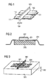
- FIG. 1 10 shows semiconductor light emitting devices 101 and 111, claddings of the semiconductor light emitting devices constituting fluorescent converter layers 102 and 112 and an optical attenuator 103.
- the semiconductor devices emit radiation in a certain wavelength range upon application of a voltage.
- the claddings contain a converter material which, when excited by electromagnetic radiation of a particular wavelength range, emits radiations of particular wavelengths.
- the converter material may contain at least one phosphor. Suitable phosphors are, for example, inorganic or organic phosphors.
- the wavelength ranges of the exciting and the emitted radiation differ.
- the cladding can either convert all of the incident radiation to it, it can also convert only a portion of the incoming radiation and transmit the remainder without significantly affecting the wavelength range of the transmitted radiation.
- the damping element is used for optical separation of the sheaths or sheaths and the semiconductor devices. It is as impermeable as possible to the wavelength ranges emitted by the semiconductor devices and the cladding.
- the damping element is arranged between two rows of semiconductor components with respective sheaths and largely prevents the converter material from being excited by the emitted radiation of adjacently arranged semiconductor components and / or their converter layers in claddings, to the associated semiconductor components of which no voltage is applied.
- a plurality of further damping elements may be arranged between further rows in order to optically isolate the further rows from one another.
- the damping element may also be designed in the form of a grid, so that each semiconductor component with respective claddings is substantially optically separated from the remaining adjacent semiconductor components and their cladding.
- the damping element can also be designed so that fields of light-emitting semiconductor components are separated from each other by respective sheaths.
- a width 104 of the damping element is as small as possible, so that the semiconductor devices can be arranged close to each other. This results in a homogeneous-looking illumination of the arrangement result. Also, a relatively high contrast between semiconductor devices that emit radiation and semiconductor devices to which no voltage is applied can be achieved. The contrast value is above 100: 1 if possible, for example at 200: 1.
- FIG. 2 1 shows a schematic representation of a light-emitting semiconductor component 201, a fluorescence converter layer 202, electrical lines 204 and a carrier element 205.
- the fluorescence converter layer is arranged on the light-emitting semiconductor component such that radiation emitted by the semiconductor component converts can be.
- the semiconductor component is arranged on the carrier element and electrically conductively connected to the lines.
- a voltage can be applied to the semiconductor device.
- the radiation emitted by the semiconductor component when the voltage is applied lies in the blue color range, for example at 445 nm.
- the converter substance can be excited by the primary radiation emitted by the light-emitting semiconductor component and emits secondary radiation.
- the wavelength range of the secondary radiation is in the yellow color range, ie between 560 and 590 nm.
- the converter substance can emit radiation which lies in different wavelength ranges, for example in the red (625 to 740 nm) and in the green (520 to 560 nm) color range.
- the primary radiation and the secondary radiation have different wavelength ranges.
- a portion of the primary radiation is transmitted through the converter substance without wavelength conversion.
- the primary radiation and the secondary radiation mix additively.
- a desired resulting color locus for example white, may be adjusted, for example, by adjusting a mixing ratio of the primary radiation and secondary radiation.
- the converter substance can also convert all the primary radiation.
- the secondary radiation consists of radiation of different wavelengths, which together give the desired color location.
- Radiation in the blue color range mixed with radiation in the yellow color range results in white light.
- Radiation in the red Color range mixed with radiation in the green color range gives yellow light.
- Radiation in the blue, red and green color range results in mixed white light.
- the carrier element can serve to derive the heat arising in the light-emitting semiconductor component.
- it is made of a sufficiently good heat conducting material, such as a ceramic.
- FIG. 3 shows light emitting semiconductor devices with claddings containing fluorescent converter layers 301, an optical attenuator 303, electrical leads 304, and a support member 305.
- the semiconductor devices are disposed on the support member and can be powered by the leads.
- the damping element is formed in one piece with the carrier element.
- an increase of the carrier element is formed when the carrier element is produced at the location between the semiconductor components. In order to achieve the desired narrow pitch of the semiconductor devices, this increase is made as thin as possible.
- the elevation may be coated with an opaque material to increase the optical attenuation effect, for example, a metal layer may be electroplated.
- the elevation of the support member separates two rows of semiconductor devices.
- the damping element can also be designed such that each semiconductor component with respective cladding is optically separated from the remaining adjacent semiconductor components and their cladding.
- the damping element can also be designed such that certain fields of semiconductor components are optically separated from one another.
- a height 302 of the damping element is at least so high that the light-emitting Semiconductor devices with the respective shells are sufficiently isolated from each other, so no fluorescence converter layers are unintentionally excited.
- FIG. 4 which is not part of the present invention, shows semiconductor light emitting devices 401, enclosures, a frame 402, potting material 403, electrical leads 404, and a support member 405.
- the claddings contain fluorescent converter layers.
- the semiconductor components are arranged on the carrier element and can be supplied with voltage via the lines.
- the frame is formed around an area in which the semiconductor devices are arranged. The frame is used to keep areas of the potting material, which should not be covered by the potting material.
- the potting material covers the area within the frame so high that the light emitting semiconductor devices and the corresponding cladding with fluorescence converter material are optically isolated, however maximally up to a height of a surface 406 of the semiconductor light emitting devices and the cladding from which radiation is emitted.
- a light-permeable encapsulation for protecting the semiconductor components may be applied over the light-emitting semiconductor components and the potting compound on the side of the surface 406.
- the frame in this case must be designed so high that the translucent potting material spreads only within the frame and areas are kept free of the translucent potting material, which should not be covered by the potting material.
- FIG. 5 which is not part of the present invention, shows light-emitting semiconductor devices with claddings, bonding wires 502, a housing body 503, electrical leads 504, and a support member 505.
- the claddings contain fluorescent converter layers.
- the semiconductor devices with the fluorescence converter layers are arranged on the carrier element and can be supplied with voltage via the lines and the bonding wires.
- the housing body is, for example, made of plastic as opaque as possible and surrounds the light-emitting semiconductor components, the fluorescent converter layers, the carrier element and partially the lines. As a result of the design of the housing body between the light-emitting semiconductor components with respective sheaths, these are optically isolated from one another.
- the plastic body fulfills a function of a protective body in addition to the optical separation.
- the housing body serves, for example, to protect the lines and the semiconductor components from external influences and to simplify the handling of the arrangement, for example during assembly.
- FIG. 6 shows coated semiconductor light emitting devices 601, a cover 602, an optical attenuator 603, electrical leads 604 and a support member 605 according to an embodiment of the present invention.
- the sheaths contain fluorescent converter layers.
- the semiconductor components are arranged on the carrier element and can be supplied with voltage via the lines.
- the cover is made of a translucent material, such as glass, such as BF33 or Pyrex, and serves to protect the semiconductor devices from external influences.
- the optical damping element is arranged as part of the cover.
- the cover is not shown in its final position, but at a greater distance from the semiconductor devices and the carrier element.
- a height 606 of the damping member is so high that, when the cover is disposed in its intended position, the damping member causes optical separation of the semiconductor devices and the respective claddings.
- the damping element extends between the sheaths, in a further embodiment the damping element reaches between the sheaths and the light-emitting semiconductor components.
- the damping element thus reduces an optical coupling of a radiation emitted by at least one of the sheaths into at least one other of the sheaths.
- the damping element can also reduce the optical coupling of a radiation emitted by at least one of the semiconductor components into the cladding of at least one of the other semiconductor components.
- two rows of light-emitting semiconductor components with fluorescence converter layers are insulated from one another by the optical damping element.
- Additional optical damping elements may be arranged to isolate more than two rows of semiconductor devices with respective claddings from one another.
- the damping element may, as in the embodiment shown, be cuboid, the damping element may also have other shapes, for example triangular in cross section.
- the shape is designed such that the light-emitting semiconductor components can be arranged as close to each other as possible.
- a width 607 is in a range of, for example 0.05 mm to 0.3 mm, the height in a range of 0.2 mm to 0.8 mm.
- the damping element is connected, for example, by an anodic bond with the cover and may in one embodiment consist of silicon.
- FIG. 7 shows a cover 702 with a divider 701 according to an embodiment of the present invention.
- the damping element is designed in the form of a grid, so that light-emitting semiconductor components are optically isolated from the adjacent semiconductor components when the cover is arranged in its intended position for the protection of semiconductor components.
- the damping element can also be designed such that rows of light-emitting semiconductor components with respective fluorescence converter layers are isolated from one another.
- the cover is made of a translucent material, such as glass.
- the damping element can be etched from a cover which is applied on the cover as opaque as possible.
- the most opaque coating possible is a silicon coating, which is, for example, anodically bonded to the cover.
- the damping element is made of plastic and, for example glued or printed on the cover.
- FIG. 8 shows a coated formation 801 of a cover 802 according to an embodiment of the present invention.
- the cover is made of translucent material.
- the formation is coated as light-impermeable as possible, for example with a metal structure.
- the formation of the cover is so high that it optically isolates the claddings of the semiconductor light-emitting devices when the cover is placed in its intended position to protect semiconductor devices.
- the damping element is lattice-shaped, so that light-emitting Semiconductor devices are optically isolated from the adjacent semiconductor devices.
- the damping element can also be designed such that rows of light-emitting semiconductor components with respective fluorescence converter layers are isolated from one another.
- Figure 9A shows light-emitting semiconductor devices 901 and 911, cladding with fluorescent converter layers 902 and 912, leads 904, bonding wires 905, and a protection element 906.
- the semiconductor devices with fluorescence converter layers are connected to a leadframe formed of leads 904 , for example by gluing or soldering.
- a protective element for example a protective film, is applied to the surface of the light-emitting semiconductor components and the cladding opposite the leadframe, which protects the semiconductor components and the cladding from damage, for example scratching, in the following method steps.
- FIG. 9B which is also not part of the present invention, shows an injection mold 907, which terminates relatively accurately on one side with the protective element, on another side with the lead frame.
- the plastic body produced in the process can optically separate the light-emitting semiconductor components and the respective claddings.
- a side of the leadframe opposite to the semiconductor devices and the side of the semiconductor light emitting devices from which radiation is emitted are not covered by the potting material.
- FIG. 9C which is also not part of the present invention, shows a plastic body 903 surrounding the light emitting semiconductor devices with the respective cladding.
- the plastic body has a shape that was given to it by the injection mold and covers neither the Semiconductor devices opposite side of the lead frame nor the surface of the semiconductor devices is emitted from the radiation.
- the plastic body optically separates the light-emitting semiconductor components and the respective claddings.
- FIG. 9D which is also not part of the present invention, shows the arrangement after the protective element has been removed. This step can be omitted if the protective element is sufficiently transparent. In this case, the translucent protective element may remain in the arrangement.
- Figure 10A which is also not part of the present invention, shows light-emitting semiconductor devices with fluorescence converter layers 105, a support member 106 and electrical leads 107.
- the light-emitting semiconductor devices with the fluorescence converter layers are deposited on the support member.
- a voltage can be applied via the cables.
- 2 ⁇ 2 semiconductor devices are arranged with respective cladding.
- pluralities of semiconductor devices are disposed on the carrier element, such as an array of 13 x 66 semiconductor devices with respective claddings.
- a damping element 108 is arranged between the two rows of light-emitting semiconductor devices with fluorescence converter layers.
- the damping element is so high that it separates the light-emitting semiconductor components and the respective claddings from each other.
- two rows of semiconductor light emitting devices are optically isolated from each other.
- the damping element can also be formed in a grid shape and optically isolate the semiconductor devices from their respective neighbors.
- the damping element can be arranged on the carrier element before the carrier element is equipped with the light-emitting semiconductor components.
- a support element with damping element shows FIG. 10C , which is also not part of the present invention.
- FIG. 10C shows a carrier element with lines and chip pads 109.
- the damping element is arranged between the chip pads. If semiconductor components are applied to the carrier element, this leads to an arrangement as in FIG. 10B shown.
- the carrier element and the damping element can be formed as one piece, for example, made of ceramic and then be equipped with semiconductor devices.
- Figure 11A which is also not part of the present invention, shows light-emitting semiconductor devices with fluorescence converter layers 113, a frame 114, potting material 115, electrical leads 116, a support member 117 and a template 118.
- the semiconductor devices are disposed on the support member and can be energized via the leads be supplied.
- the frame is disposed on the support member so as to surround an area to be filled with the potting material.
- the potting material is printed on the carrier element by means of stencil printing via the template.
- the template has holes where potting material is to be printed.
- the potting material continues to spread after printing on the support member until it is cured.
- the frame limits the spreading of the potting material.
- the potting material should be a surface 119 of the semiconductor devices, is emitted from the radiation, do not cover.
- FIG. 11B which is also not part of the present invention, shows the arrangement with a potting body 110 of the potting material 115, the support member and the semiconductor devices with enclosures.
- the potting body was printed on the assembly. Only the surfaces 119 of the semiconductor devices with fluorescence converter layers, from which radiation emerges, remain free. The other surfaces are surrounded by the potting material.
- the frame determines which areas on the carrier element are covered with potting compound.
- the frames may be arranged on the carrier element in order to be able to form a plurality of potting bodies on the carrier element.
- the frames each include a region in which the potting body is formed for the optical isolation of the light-emitting semiconductor components arranged in the region with fluorescence converter layers.
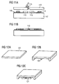
- FIG. 12A shows a translucent cover 122 according to an embodiment of the present invention.
- the cover serves to protect an arrangement of semiconductor devices with fluorescence converter layers from external influences. It is translucent, absorbs and therefore reflects as little radiation as possible in the wavelength ranges in which the semiconductor components and the fluorescence converter layers emit.
- the ranges of the radiation emitted by the array in the visible range between about 380 nm and 780 nm.
- the cover can also be translucent for radiation in the infrared range (780 nm to 1 mm) or in the ultraviolet range (1 nm to 380 nm).
- the cover may perform optical functions, for example, it may be formed as a lens or contain areas that act as lenses.
- FIG. 12B shows damping elements 123, according to an embodiment of the present invention. These are as opaque as possible and arranged at the locations of the cover, at which an optical separation of semiconductor light-emitting devices to be covered by the cover, is provided.
- the damping elements are formed so that the semiconductor components to be covered can be arranged as close to each other as possible.
- the damping elements may, for example, be connected to the cover by anodic bonding, for example the damping elements are anodically bonded silicon strips.
- the damping elements are glued to the cover, in another embodiment, the damping elements are printed on the cover.
- the damping elements have been formed when embossing the cover as a formation of the cover.
- These embodiments are coated with an opaque material, such as galvanic with a metal structure.
- FIG. 12C shows semiconductor light-emitting devices with fluorescent converter layers 121 covered by a cover with damping elements according to the present invention.
- the cover is over so arranged the semiconductor devices with fluorescence converter layers that the damping elements lie between them and these optically separate from adjacent semiconductor devices and fluorescence converter layers.
- FIG. 13A shows, according to an embodiment of the present invention, a translucent cover 132 and a possible opaque layer 131.
- the cover is connected to the layer.
- the cover is formed, for example, of glass.
- the layer is, for example, a silicon layer, which is anodically bonded to the cover.
- FIG. 13B shows an etching mask 134.
- the etching mask is used for fürlochticianung and is formed so that after an etching process damping elements remain at the locations of the glass cover, where semiconductor devices with fluorescence converter layers are to be optically isolated from each other.
- the etching mask consists for example of silicon oxide (SiO) or silicon nitride (SiN).
- SiO silicon oxide
- SiN silicon nitride
- wedge-shaped damping elements can be formed. These form, for example, an angle of 54.7 °.
- the etching material is, for example, potassium hydroxide (KOH) or ethylenediamine pyrocatechol (EDP).
- KOH potassium hydroxide
- EDP ethylenediamine pyrocatechol
- FIG. 13C shows, according to an embodiment of the present invention, the cover with a damping element 133 after the etching process.
- the damping elements are formed in a wedge shape at the locations where an optical separation of semiconductor devices to be covered by the cover is desired. They are high enough to be between Envelopes of the semiconductor devices and the semiconductor devices to reach. They have a shape that enables a closely adjacent arrangement of the semiconductor components to be covered.
Description
Die Erfindung betrifft eine Anordnung mit mindestens zwei lichtemittierenden Halbleiterbauelementen und ein Verfahren zur Herstellung einer Anordnung mit mindestens zwei lichtemittierenden Halbleiterbauelementen.The invention relates to an arrangement having at least two light-emitting semiconductor components and to a method for producing an arrangement having at least two light-emitting semiconductor components.
Um mit Hilfe von lichtemittierenden Halbleiterbauelementen weißes Licht zu erzeugen, werden die lichtemittierende Halbleiterbauelemente mit einer Umhüllung versehen, die eine Konvertersubstanz enthält. Diese Konvertersubstanz konvertiert die vom Halbleiterbauelement emittierte Strahlung eines ersten Wellenlängenbereichs (Primärstrahlung) in Strahlung eines zweiten Wellenlängenbereichs (Sekundärstrahlung), der sich von dem ersten Bereich unterscheidet. Weißes Licht kann auf diese Art entweder erzeugt werden, indem Primärstrahlung mit der Sekundärstrahlung gemischt wird, oder indem die Farbanteile der konvertierten Strahlung zusammengemischt weißes Licht ergeben.In order to produce white light by means of light-emitting semiconductor components, the light-emitting semiconductor components are provided with a cladding which contains a converter substance. This converter substance converts the radiation emitted by the semiconductor component of a first wavelength range (primary radiation) into radiation of a second wavelength range (secondary radiation), which differs from the first range. White light can be generated in this way either by mixing primary radiation with the secondary radiation or by mixing the color components of the converted radiation together to give white light.
Wenn mehrere lichtemittierende Halbleiterbauelemente mit Konverterumhüllung benachbart angeordnet werden, kann es durch die Strahlung benachbarter lichtemittierender Bauelemente zu einer Anregung der Konvertersubstanz von Halbleiterbauelementen kommen, an die keine Spannung angelegt ist. Dieses Mitleuchten führt dazu, dass Anwendungen, die eine genaue Trennung zwischen hellen und dunklen Bereichen benötigen, nur mit hohem Aufwand realisiert werden können.If a plurality of semiconductor light-emitting devices with converter cladding are arranged adjacent, it may be due to the radiation of adjacent light emitting devices an excitation of the converter substance of semiconductor devices come to which no voltage is applied. This illumination means that applications that require a precise separation between light and dark areas can only be realized with great effort.
In der Druckschrift
Aus der Druckschrift
In der Druckschrift
Es ist eine Aufgabe der Erfindung, eine Anordnung mit mindestens zwei lichtemittierenden Halbleiterbauelementen sowie ein verfahren zur Herstellung einer Anordnung mit mindestens zwei lichtemittierenden Halbleiterbauelementen anzugeben, das sich einfacher und kostengünstiger herstellen lässt.It is an object of the invention to provide an arrangement with at least two light-emitting semiconductor components and a method for producing an arrangement with at least two light-emitting semiconductor components, which can be produced in a simpler and less expensive manner.
Die Aufgaben wird gelöst durch eine Anordnung mit den Merkmalen des Anspruchs 1 beziehungsweise ein Verfahren mit den Merkmalen des Anspruchs 8.The objects are achieved by an arrangement having the features of claim 1 or a method having the features of claim 8.
Eine Anordnung mit mindestens zwei benachbart zueinander angeordneten lichtemittierenden Halbleiterbauelementen weist Umhüllungen auf, die jeweils die mindestens zwei lichtemittierenden Halbleiterbauelemente zumindest teilweise umgeben. In den Umhüllungen ist eine Konvertersubstanz enthalten, die den Wellenlängenbereich der von den Halbleiterbauelementen emittierten Strahlung teilweise oder vollständig konvertiert. Die Anordnung weist mindestens ein optisches Dämpfelement auf, das zwischen den mindestens zwei lichtemittierenden Halbleiterbauelementen angeordnet ist. Das Dämpfelement isoliert die jeweiligen Umhüllungen optisch, um eine optische Einkopplung einer von mindestens einem der Halbleiterbauelemente emittierten Strahlung in die Umhüllung mindestens eines der anderen Halbleiterbauelemente zu verringern. Das Dämpfelement kann auch die optische Einkopplung einer von mindestens einer der Umhüllungen emittierten Strahlung in mindestens eine andere der Umhüllungen verringern.An arrangement with at least two light-emitting semiconductor components arranged adjacent to one another has Envelopes which each at least partially surround the at least two light-emitting semiconductor components. The cladding contains a converter substance which partially or completely converts the wavelength range of the radiation emitted by the semiconductor components. The arrangement has at least one optical damping element which is arranged between the at least two light-emitting semiconductor components. The damping element optically isolates the respective cladding to reduce optical coupling of radiation emitted by at least one of the semiconductor devices into the cladding of at least one of the other semiconductor devices. The damping element may also reduce the optical coupling of radiation emitted by at least one of the claddings into at least one other of the claddings.
Das optische Dämpfelement ist als Teil einer lichtdurchlässigen Abdeckung, die zum Schutz der Halbleiterbauelemente über den Halbleiterbauelementen angeordnet ist, gebildet.The optical damping element is formed as part of a light-transmitting cover, which is arranged to protect the semiconductor components over the semiconductor devices.
In einer Ausführungsform wird ein Siliziumstreifen, der so hoch ist, dass er die Umhüllungen optisch isoliert mit der Abdeckung verbunden, beispielsweise durch eine anodische Bondverbindung.In one embodiment, a silicon strip that is high enough to optically isolate the cladding is connected to the cover, such as an anodic bond.
In einer weiteren Ausführungsform wird ein Körper aus einem gespritzten Kunststoff mit der Abdeckung verbunden, beispielsweise auf die Abdeckung geklebt oder gedruckt.In a further embodiment, a body of a molded plastic is connected to the cover, for example glued or printed on the cover.
Das Dämpfelement kann eine Ausformung der Abdeckung sein, die mit der Abdeckung aus einem Stück ausgebildet ist. Diese Ausformung ist mit einer lichtundurchlässigen Beschichtung versehen, die beispielsweise chromhaltig ist.The damping element may be a molding of the cover, which is formed with the cover in one piece. This formation is provided with an opaque coating, which is chromium-containing, for example.
In einer Ausführungsform, die nicht Teil der vorliegenden Erfindung ist, ist das Dämpfelement als Erhöhung eines Trägerelements für die mindestens zwei lichtemittierenden Halbleiterbauelemente ausgebildet. Beispielsweise sind das Trägerelement und das Dämpfelement aus einem Stück gebildet, beispielsweise aus einer Keramik. Das Dämpfelement kann, um ein Durchstrahlen durch die Erhöhung zu verringern, mit einem lichtundurchlässigen Material beschichtet sein, beispielsweise galvanisch mit einer Metallschicht. Die Erhöhung des Trägerelements reicht mindestens bis in die Höhe der Umhüllung, um diese optisch zu isolieren.In an embodiment which is not part of the present invention, the damping element is designed as an elevation of a carrier element for the at least two light-emitting semiconductor components. For example the carrier element and the damping element are formed in one piece, for example of a ceramic. The damping element may be coated with an opaque material, for example, galvanically with a metal layer, in order to reduce radiation through the elevation. The increase of the support element extends at least up to the height of the enclosure in order to visually isolate them.
In einer weiteren Ausführungsform, die ebenfalls nicht Teil der vorliegenden Erfindung ist, ist das Dämpf-element als Körper aus einem Vergussmaterial ausgebildet, der die mindestens zwei Halbleiterbauelemente und die jeweiligen Umhüllungen umgibt und die Umhüllungen optisch isoliert. Das Dämpfelement kann ein Körper aus einem Kunststoff sein, der die mindestens zwei Halbleiterbauelemente und die jeweiligen Umhüllungen umgibt und die Umhüllungen optisch isoliert.In another embodiment, which is also not part of the present invention, the damping element is formed as a body of a potting material surrounding the at least two semiconductor devices and the respective sheaths and the sheaths optically isolated. The damping element may be a body made of a plastic that surrounds the at least two semiconductor components and the respective sheaths and optically isolates the sheaths.
Bei einem Verfahren zum Herstellen einer Anordnung mit mindestens zwei benachbart angeordneten lichtemittierenden Halbleiterbauelementen werden Umhüllungen, die jeweils die zwei lichtemittierenden Halbleiterbauelemente zumindest teilweise umgeben, vorgesehen. In den Umhüllungen ist eine Konvertersubstanz enthalten, die den Wellenlängenbereich der von den Halbleiterbauelementen emittierten Strahlung teilweise oder vollständig konvertiert. Zwischen die zwei lichtemittierenden Halbleiterbauelementen wird mindestens ein optisches Dämpfelement eingebracht. Das Dämpfelement isoliert die jeweiligen Umhüllungen optisch, um eine optische Einkopplung einer von mindestens einem der Halbleiterbauelemente emittierten Strahlung in die Umhüllung mindestens eines der anderen Halbleiterbauelemente zu verringern. Das Dämpfelement kann auch die optische Einkopplung einer von mindestens einer der Umhüllungen emittierten Strahlung in mindestens eine andere der Umhüllungen verringern. Das Verfahren umfasst ein Bereitstellen einer lichtdurchlässigen Abdeckung zum Schutz der mindestens zwei Halbleiterbauelemente, ein Ausbilden mindestens eines optischen Dämpfelements an der Abdeckung und ein Anordnen der Abdeckung, so dass das mindestens eine optische Dämpfelement zwischen den mindestens zwei lichtemittierenden Halbleiterbauelementen liegt, um die jeweiligen Umhüllungen optisch zu isolieren. Beispielsweise wird das optische Dämpfelement durch anodisches Bonden mit der Abdeckung verbunden.In a method for producing an arrangement having at least two adjacently arranged light-emitting semiconductor components, envelopes which at least partially surround the two light-emitting semiconductor components are provided. The cladding contains a converter substance which partially or completely converts the wavelength range of the radiation emitted by the semiconductor components. At least one optical damping element is introduced between the two light-emitting semiconductor components. The damping element optically isolates the respective cladding to reduce optical coupling of radiation emitted by at least one of the semiconductor devices into the cladding of at least one of the other semiconductor devices. The damping element may also reduce the optical coupling of radiation emitted by at least one of the claddings into at least one other of the claddings. The method includes Providing a translucent cover for protecting the at least two semiconductor devices, forming at least one optical attenuator element on the cover, and disposing the cover such that the at least one optical attenuator is between the at least two semiconductor light emitting devices to optically isolate the respective enclosures. For example, the optical damping element is connected to the cover by anodic bonding.
Das Verfahren kann ein Ätzen des Trägerelements aus einer mit der Abdeckung verbundenen Siliziumschicht beinhalten.The method may include etching the support member from a silicon layer bonded to the cover.
Das optische Dämpfelement kann auf die Abdeckung geklebt oder gedruckt werden. In einer weiteren Ausführungsform wird die Abdeckung mit mindestens einer Ausbildung geprägt, und diese Ausbildung mit einem lichtundurchlässigen Material beschichtet.The optical damping element can be glued or printed on the cover. In a further embodiment, the cover is embossed with at least one formation, and this formation coated with an opaque material.
Das Verfahren kann ein Aufbringen der lichtemittierenden Halbleiterbauelemente auf ein Trägerelement umfassen. Das Dämpfelement ist so hoch, dass es die Umhüllungen optisch isoliert und hat eine Form, die ein Positionieren der mindestens zwei Halbleiterbauelemente im geringen Abstand zueinander ermöglicht.The method may comprise applying the light-emitting semiconductor components to a carrier element. The damping element is so high that it optically isolates the sheaths and has a shape that allows positioning of the at least two semiconductor devices at close proximity to one another.
In einer Ausführungsform, die nicht Teil der vorliegenden Erfindung ist, wird das optische Dämpfelement und das Trägerelement als ein Stück gebildet und beide werden aus dem gleichen Material hergestellt. In einer weiteren Ausführungsform, die ebenfalls nicht Teil der vorliegenden Erfindung ist, umfasst das Verfahren ein Siebdrucken eines Vergussmaterials zwischen die mindestens zwei lichtemittierenden Halbleiterbauelemente. Das Verfahren kann ein Umspritzen der lichtemittierenden Halbleiterbauelemente mit einem Kunststoff aufweisen, so dass der Kunststoff die Umhüllung optisch isoliert.In one embodiment, which is not part of the present invention, the optical damping element and the carrier element are formed as one piece and both are made of the same material. In a further embodiment, which is also not part of the present invention, the method comprises screen-printing a potting material between the at least two light-emitting semiconductor components. The method may include overmolding the light-emitting semiconductor components Having a plastic, so that the plastic, the sheath optically isolated.
Weitere Merkmale, Vorteile und Weiterbildungen ergeben sich aus den nachfolgenden in Verbindung mit den
Es zeigen:
- Figur 1
- eie schematische Darstellung einer Anordnung die ein Prinzip der vorliegenden Erfindung darstellt,
- Figur 2
- eine schematische Darstellung eines lichtemittierenden Halbleiterbauelements,
- Figur 3
- eine schematische Darstellung, die nicht Teil der vorliegenden Erfindung ist, eines Trägerelements mit einem Dämpfelement,
- Figur 4
- eine schematische Darstellung einer Anordnung gemäß einer Ausführungsform, die nicht Teil der vorliegenden Erfindung ist, mit einem Körper aus vergussmaterial,
- Figur 5
- eine schematische Darstellung einer Anordnung gemäß einer Ausführungsform, die ebenfalls nicht Teil der vorliegenden Erfindung ist, mit einem Kunststoffkörper,
- Figur 6
- eine schematische Darstellung eines Trägerelements sowie einer lichtdurchlässigen Abdeckung, an der ein Dämpfelement angeordnet ist, gemäß einer Ausführungsform der vorliegenden Erfindung,
- Figur 7
- eine schematische Darstellung einer lichtdurchlässigen Abdeckung, auf die ein Dämpfelement aufgebracht ist, gemäß einer Ausführungsform der vorliegenden Erfindung,
- Figur 8
- eine schematische Darstellung einer lichtdurchlässigen Abdeckung, die zusammen mit einer Ausformung geprägt ist, gemäß einer Ausführungsform der vorliegenden Erfindung,
- Figuren 9A bis 9D
- eine schematische Darstellung eines Ausführungsbeispiels, das nicht Teil der vorliegenden Erfindung ist, für ein Verfahren zum Umgießen von Halbleiterbauelementen mit Umhüllungen,
- Figuren 10A bis 10C
- eine schematische Darstellung eines Verfahrens, das nicht Teil der vorliegenden Erfindung ist, bei dem ein Dämpfelement auf einem Träger-element angeordnet wird,
- Figuren 11A und 11B
- eine schematische Darstellung eines Ausführungsbeispiels für ein Siebdruckverfahren, das nicht Teil der vorliegenden Erfindung ist,
- Figuren 12A bis 12C
- eine schematische Darstellung eines Ausführungsbeispiels für ein Verfahren gemäß der vorliegenden Erfindung, bei dem das optische Dämpfelement auf einer lichtdurchlässigen Abdeckung angeordnet wird, und
- Figuren 13A bis 13C
- eine schematische Darstellung eines Ausführungsbeispiels eines Ätzverfahrens gemäß der vorliegenden Erfindung.
- FIG. 1
- a schematic representation of an arrangement which represents a principle of the present invention,
- FIG. 2
- a schematic representation of a light-emitting semiconductor device,
- FIG. 3
- a schematic representation, which is not part of the present invention, a support member having a damping element,
- FIG. 4
- 1 is a schematic representation of an arrangement according to an embodiment, which is not part of the present invention, with a body of potting material,
- FIG. 5
- 1 is a schematic representation of an arrangement according to an embodiment, which is also not part of the present invention, with a plastic body,
- FIG. 6
- a schematic representation of a support member and a translucent cover, on which a damping element is arranged, according to an embodiment of the present invention,
- FIG. 7
- a schematic representation of a translucent cover, on which a damping element is applied, according to an embodiment of the present invention,
- FIG. 8
- a schematic representation of a translucent cover, which is coined together with a molding, according to an embodiment of the present invention,
- FIGS. 9A to 9D
- 1 is a schematic representation of an embodiment, which is not part of the present invention, for a method for encapsulating semiconductor devices with claddings,
- FIGS. 10A to 10C
- a schematic representation of a method, which is not part of the present invention, in which a damping element is arranged on a support element,
- Figures 11A and 11B
- a schematic representation of an embodiment of a screen printing method, which is not part of the present invention,
- FIGS. 12A to 12C
- a schematic representation of an embodiment of a method according to the present invention, in which the optical Damping element is placed on a translucent cover, and
- FIGS. 13A to 13C
- a schematic representation of an embodiment of an etching method according to the present invention.
Die Wellenlängenbereiche der anregenden und der emittierten Strahlung unterscheiden sich. Die Umhüllung kann entweder die gesamte auf sie eintreffende Strahlung umwandeln, sie kann auch nur einen Teil der eintreffenden Strahlung konvertieren und den übrigen Teil durchlassen, ohne den Wellenlängenbereich der durchgelassenen Strahlung signifikant zu beeinflussen.The wavelength ranges of the exciting and the emitted radiation differ. The cladding can either convert all of the incident radiation to it, it can also convert only a portion of the incoming radiation and transmit the remainder without significantly affecting the wavelength range of the transmitted radiation.
Das Dämpfelement dient zur optischen Trennung der Umhüllungen oder der Umhüllungen und der Halbleiterbauelemente. Es ist für die Wellenlängenbereiche, die von den Halbleiterbauelementen und den Umhüllungen emittiert wird, möglichst undurchlässig.The damping element is used for optical separation of the sheaths or sheaths and the semiconductor devices. It is as impermeable as possible to the wavelength ranges emitted by the semiconductor devices and the cladding.
In dem gezeigten Beispiel ist das Dämpfelement zwischen zwei Reihen von Halbleiterbauelementen mit jeweiligen Umhüllungen angeordnet und verhindert weitestgehend, dass durch die emittierte Strahlung benachbart angeordneter Halbleiterbauelemente und/oder deren Konverterschichten Konvertermaterial in Umhüllungen angeregt wird, an deren dazugehörigen Halbleiterbauelementen keine Spannung angelegt ist.In the example shown, the damping element is arranged between two rows of semiconductor components with respective sheaths and largely prevents the converter material from being excited by the emitted radiation of adjacently arranged semiconductor components and / or their converter layers in claddings, to the associated semiconductor components of which no voltage is applied.
Es können eine Vielzahl weiterer Dämpfelemente zwischen weiteren Reihen angeordnet sein, um die weiteren Reihen optisch voneinander zu isolieren. Das Dämpfelement kann auch gitterförmig ausgebildet sein, so dass jedes Halbleiterbauelement mit jeweiligen Umhüllungen von den übrigen benachbarten Halbleiterbauelementen und deren Umhüllungen im Wesentlichen optisch getrennt ist. Das Dämpfelement kann auch so ausgebildet sein, dass Felder von lichtemittierenden Halbleiterbauelementen mit jeweiligen Umhüllungen voneinander getrennt werden.A plurality of further damping elements may be arranged between further rows in order to optically isolate the further rows from one another. The damping element may also be designed in the form of a grid, so that each semiconductor component with respective claddings is substantially optically separated from the remaining adjacent semiconductor components and their cladding. The damping element can also be designed so that fields of light-emitting semiconductor components are separated from each other by respective sheaths.
Eine Breite 104 des Dämpfelements ist möglichst gering, damit die Halbleiterbauelemente nahe aneinander angeordnet werden können. Dies hat ein homogen wirkendes Leuchtbild der Anordnung zur Folge. Auch ein relativ hoher Kontrast zwischen Halbleiterbauelementen, die Strahlung emittieren, und Halbleiterbauelementen, an die keine Spannung angelegt ist, kann erreicht werden. Der Kontrastwert liegt möglichst über 100:1, beispielsweise bei 200:1.A
Über die Leitungen kann an dem Halbleiterbauelement eine Spannung angelegt werden. Die von dem Halbleiterbauelement bei angelegter Spannung emittierte Strahlung liegt in einer Ausführungsform im blauen Farbbereich, beispielsweise bei 445 nm. Die Konvertersubstanz ist durch die von dem lichtemittierenden Halbleiterbauelement emittierte Primärstrahlung anregbar und emittiert eine Sekundärstrahlung. In einer Ausführungsform liegt der Wellenlängenbereich der Sekundärstrahlung im gelben Farbbereich, also zwischen 560 und 590 nm. Die Konvertersubstanz kann in einer weiteren Ausführungsform Strahlung emittieren, die in unterschiedlichen Wellenlängenbereichen liegt, beispielsweise im roten (625 bis 740 nm) und im grünen (520 bis 560 nm) Farbbereich.Via the lines, a voltage can be applied to the semiconductor device. In one embodiment, the radiation emitted by the semiconductor component when the voltage is applied lies in the blue color range, for example at 445 nm. The converter substance can be excited by the primary radiation emitted by the light-emitting semiconductor component and emits secondary radiation. In one embodiment, the wavelength range of the secondary radiation is in the yellow color range, ie between 560 and 590 nm. In a further embodiment, the converter substance can emit radiation which lies in different wavelength ranges, for example in the red (625 to 740 nm) and in the green (520 to 560 nm) color range.
Die Primärstrahlung und die Sekundärstrahlung weisen unterschiedliche Wellenlängenbereiche auf. Ein Teil der Primärstrahlung wird ohne Wellenlängenkonversion durch die Konvertersubstanz durchgelassen. Die Primärstrahlung und die Sekundärstrahlung mischen sich additiv. Ein gewünschter resultierender Farbort, beispielsweise weiß, kann beispielsweise durch ein Einstellen eines Mischungsverhältnisses der Primärstrahlung und Sekundärstrahlung eingestellt werden. Die Konvertersubstanz kann auch die gesamte Primärstrahlung umwandeln. In diesem Fall besteht die Sekundärstrahlung aus Strahlung unterschiedlicher Wellenlängen, die zusammengemischt den gewünschten Farbort ergeben.The primary radiation and the secondary radiation have different wavelength ranges. A portion of the primary radiation is transmitted through the converter substance without wavelength conversion. The primary radiation and the secondary radiation mix additively. A desired resulting color locus, for example white, may be adjusted, for example, by adjusting a mixing ratio of the primary radiation and secondary radiation. The converter substance can also convert all the primary radiation. In this case, the secondary radiation consists of radiation of different wavelengths, which together give the desired color location.
Strahlung im blauen Farbbereich gemischt mit Strahlung im gelben Farbbereich ergibt weißes Licht. Strahlung im roten Farbbereich gemischt mit Strahlung im grünen Farbbereich ergibt gelbes Licht. Strahlung im blauen, roten und grünen Farbbereich ergibt gemischt weißes Licht.Radiation in the blue color range mixed with radiation in the yellow color range results in white light. Radiation in the red Color range mixed with radiation in the green color range gives yellow light. Radiation in the blue, red and green color range results in mixed white light.
Das Trägerelement kann zum Ableiten der im lichtemittierenden Halbleiterbauelement entstehenden Wärme dienen. Dazu ist es aus einem ausreichend gut wärmeleitenden Material gefertigt, beispielsweise einer Keramik.The carrier element can serve to derive the heat arising in the light-emitting semiconductor component. For this purpose it is made of a sufficiently good heat conducting material, such as a ceramic.
In der gezeigten Ausführungsform, die nicht Teil der vorliegenden Erfindung ist, trennt die Erhöhung des Trägerelements zwei Zeilen von Halbleiterbauelementen. Das Dämpfelement kann aber auch so ausgebildet sein, dass jedes Halbleiterbauelement mit jeweiliger Umhüllung von den übrigen benachbarten Halbleiterbauelementen und deren Umhüllungen optisch getrennt ist. Das Dämpfelement kann auch so ausgebildet sein, dass bestimmte Felder von Halbleiterbauelementen optisch voneinander getrennt werden. Eine Höhe 302 des Dämpfelements ist mindestens so hoch, dass die lichtemittierenden Halbleiterbauelemente mit den jeweiligen Umhüllungen ausreichend voneinander isoliert werden, also keine Fluoreszenzkonverterschichten ungewollt angeregt werden.In the illustrated embodiment, which is not part of the present invention, the elevation of the support member separates two rows of semiconductor devices. However, the damping element can also be designed such that each semiconductor component with respective cladding is optically separated from the remaining adjacent semiconductor components and their cladding. The damping element can also be designed such that certain fields of semiconductor components are optically separated from one another. A
Das Vergussmaterial bedeckt den Bereich innerhalb des Rahmens so hoch, dass die lichtemittierenden Halbleiterbauelemente und die entsprechenden Umhüllungen mit Fluoreszenzkonvertermaterial optisch isoliert sind, maximal jedoch bis auf eine Höhe einer Oberfläche 406 der lichtemittierenden Halbleiterbauelemente und der Umhüllungen, aus der Strahlung emittiert wird.The potting material covers the area within the frame so high that the light emitting semiconductor devices and the corresponding cladding with fluorescence converter material are optically isolated, however maximally up to a height of a
Zusätzlich zum möglichst lichtundurchlässigen Vergusskörper kann über den lichtemittierenden Halbleiterbauelementen und der Vergussmasse auf der Seite der Oberfläche 406 ein lichtdurchlässiger Verguss zum Schutz der Halbleiterbauelemente aufgebracht sein. Der Rahmen muss in diesem Fall so hoch ausgebildet sein, dass sich das lichtdurchlässige Vergussmaterial nur innerhalb des Rahmens ausbreitet und Bereiche von dem lichtdurchlässige Vergussmaterial freigehalten sind, die nicht von dem Vergussmaterial bedeckt werden sollen.In addition to the optionally opaque encapsulation body, a light-permeable encapsulation for protecting the semiconductor components may be applied over the light-emitting semiconductor components and the potting compound on the side of the
Der Kunststoffkörper erfüllt zusätzlich zum optischen Trennen eine Funktion eines Schutzkörpers. Der Gehäusekörper dient beispielsweise zum Schutz der Leitungen und der Halbleiterbauelemente vor äußeren Einflüssen sowie dazu, die Handhabung der Anordnung, beispielsweise während einer Montage, zu vereinfachen.The plastic body fulfills a function of a protective body in addition to the optical separation. The housing body serves, for example, to protect the lines and the semiconductor components from external influences and to simplify the handling of the arrangement, for example during assembly.
Das optische Dämpfelement wird als Teil der Abdeckung angeordnet. In der Figur ist die Abdeckung nicht in ihrer endgültigen Position gezeigt, sondern in größerem Abstand zu den Halbleiterbauelementen und dem Trägerelement. Eine Höhe 606 des Dämpfelements ist so hoch, dass das Dämpfelement, wenn die Abdeckung in ihrer vorgesehenen Position angeordnet ist, eine optische Trennung der Halbleiterbauelemente und der jeweiligen Umhüllungen bewirkt.The optical damping element is arranged as part of the cover. In the figure, the cover is not shown in its final position, but at a greater distance from the semiconductor devices and the carrier element. A
In einer Ausführungsform reicht das Dämpfelement bis zwischen die Umhüllungen, in einer weiteren Ausführungsform reicht das Dämpfelement bis zwischen die Umhüllungen und die lichtemittierenden Halbleiterbauelemente. Das Dämpfelement verringert so eine optische Einkopplung einer von mindestens einer der Umhüllungen emittierten Strahlung in mindestens eine andere der Umhüllungen. Das Dämpfelement kann auch die optische Einkopplung einer von mindestens einem der Halbleiterbauelemente emittierten Strahlung in die Umhüllung mindestens eines der anderen Halbleiterbauelemente verringern.In one embodiment, the damping element extends between the sheaths, in a further embodiment the damping element reaches between the sheaths and the light-emitting semiconductor components. The damping element thus reduces an optical coupling of a radiation emitted by at least one of the sheaths into at least one other of the sheaths. The damping element can also reduce the optical coupling of a radiation emitted by at least one of the semiconductor components into the cladding of at least one of the other semiconductor components.
Im gezeigten Ausführungsbeispiel werden durch das optische Dämpfelement zwei Reihen lichtemittierende Halbleiterbauelemente mit Fluoreszenzkonverterschichten von einander isoliert. Es können weitere optische Dämpfelemente angeordnet sein, um mehr als zwei Reihen von Halbleiterbauelementen mit jeweiligen Umhüllungen voneinander zu isolieren.In the exemplary embodiment shown, two rows of light-emitting semiconductor components with fluorescence converter layers are insulated from one another by the optical damping element. Additional optical damping elements may be arranged to isolate more than two rows of semiconductor devices with respective claddings from one another.
Das Dämpfelement kann wie in der gezeigten Ausführungsform quaderförmig sein, das Dämpfelement kann auch andere Formen haben, beispielsweise im Querschnitt dreieckig. Die Form ist derart ausgebildet, dass die lichtemittierenden Halbleiterbauelemente möglichst nah aneinander angeordnet seien können. Eine Breite 607 liegt beispielsweise in einem Bereich von 0,05 mm bis 0,3 mm, die Höhe in einem Bereich von 0,2 mm bis 0,8 mm. Das Dämpfelement ist beispielsweise durch eine anodische Bondverbindung mit der Abdeckung verbunden und kann in einer Ausführungsform aus Silizium bestehen.The damping element may, as in the embodiment shown, be cuboid, the damping element may also have other shapes, for example triangular in cross section. The shape is designed such that the light-emitting semiconductor components can be arranged as close to each other as possible. A
Die Abdeckung ist aus einem lichtdurchlässigen Material gefertigt, beispielsweise Glas. Das Dämpfelement kann aus einer auf die Abdeckung aufgebrachten möglichst lichtundurchlässigen Beschichtung geätzt sein. Beispielsweise ist die möglichst lichtundurchlässige Beschichtung eine Siliziumbeschichtung, die beispielsweise anodisch auf die Abdeckung gebondet ist. In einer anderen Ausführungsform ist das Dämpfelement aus Kunststoff und beispielsweise auf die Abdeckung geklebt oder gedruckt.The cover is made of a translucent material, such as glass. The damping element can be etched from a cover which is applied on the cover as opaque as possible. For example, the most opaque coating possible is a silicon coating, which is, for example, anodically bonded to the cover. In another embodiment, the damping element is made of plastic and, for example glued or printed on the cover.
In
Das Dämpfelement kann auf dem Trägerelement angeordnet werden, bevor das Trägerelement mit den lichtemittierenden Halbleiterbauelementen bestückt wird. Ein solches Trägerelement mit Dämpfelement zeigt
Das Vergussmaterial wird mittels Schablonendruck über die Schablone auf das Trägerelement gedruckt. Die Schablone hat dort Löcher, wo Vergussmaterial aufgedruckt werden soll. Das Vergussmaterial breitet sich nach dem Drucken auf dem Trägerelement weiter aus, bis es ausgehärtet ist. Der Rahmen beschränkt das Ausbreiten des Vergussmaterials. Das Vergussmaterial soll eine Oberfläche 119 der Halbleiterbauelemente, aus der Strahlung emittiert wird, nicht bedecken. Durch die über dem Trägerelement angeordnete Schablone wird soviel Vergussmasse gedruckt, dass diese auf dem Trägerelement hoch genug ist, um die Halbleiterbauelemente mit den Fluoreszenzkonverterschichten optisch zu isolieren, die Oberflächen 119 aber nicht bedeckt.The potting material is printed on the carrier element by means of stencil printing via the template. The template has holes where potting material is to be printed. The potting material continues to spread after printing on the support member until it is cured. The frame limits the spreading of the potting material. The potting material should be a
Auf dem Trägerelement können mehrere Rahmen angeordnet sein, um mehrere Vergusskörper auf dem Trägerelement ausbilden zu können. Die Rahmen schließen jeweils einen Bereich ein, in dem der Vergusskörper zur optischen Isolation der in dem Bereich angeordneten lichtemittierenden Halbleiterbauelemente mit Fluoreszenzkonverterschichten gebildet wird.Several frames may be arranged on the carrier element in order to be able to form a plurality of potting bodies on the carrier element. The frames each include a region in which the potting body is formed for the optical isolation of the light-emitting semiconductor components arranged in the region with fluorescence converter layers.
In einer Ausführungsform liegen die Bereiche der von der Anordnung emittierten Strahlung im sichtbaren Bereich, zwischen etwa 380 nm und 780 nm. Die Abdeckung kann aber auch lichtdurchlässig sein für Strahlung im Infrarotbereich (780 nm bis 1 mm) oder im ultravioletten Bereich (1 nm bis 380 nm). Die Abdeckung kann optische Funktionen erfüllen, beispielsweise kann sie als Linse ausgebildet sein oder Bereiche enthalten, die als Linsen wirken.In one embodiment, the ranges of the radiation emitted by the array in the visible range, between about 380 nm and 780 nm. The cover can also be translucent for radiation in the infrared range (780 nm to 1 mm) or in the ultraviolet range (1 nm to 380 nm). The cover may perform optical functions, for example, it may be formed as a lens or contain areas that act as lenses.
Die Dämpfelemente können beispielsweise durch anodisches Bonden mit der Abdeckung verbunden sein, beispielsweise sind die Dämpfelemente anodisch aufgebondete Siliziumstreifen. In einer anderen Ausführungsform sind die Dämpfelemente auf die Abdeckung geklebt, in einer weiteren Ausführungsform sind die Dämpfelemente auf die Abdeckung gedruckt.The damping elements may, for example, be connected to the cover by anodic bonding, for example the damping elements are anodically bonded silicon strips. In another embodiment, the damping elements are glued to the cover, in another embodiment, the damping elements are printed on the cover.
In einer weiteren Ausführungsform sind die Dämpfelemente beim Prägen der Abdeckung als Ausbildung der Abdeckung gebildet worden. Diese Ausbildungen werden mit einem lichtundurchlässigen Material beschichtet, beispielsweise galvanisch mit einer Metallstruktur.In a further embodiment, the damping elements have been formed when embossing the cover as a formation of the cover. These embodiments are coated with an opaque material, such as galvanic with a metal structure.
Die Ätzmaske besteht beispielsweise aus Siliziumoxid (SiO) oder Siliziumnitrid (SiN). Durch eine relativ schmale Maskenstruktur und eine auftretende Unterätzung der Maske, also ein Eindringen des Ätzmaterials unter die Maske, können keilförmige Dämpfelemente gebildet werden. Diese bilden beispielsweise einen Winkel von 54,7° aus. Das Ätzmaterial ist beispielsweise Kaliumhydroxid (KOH) oder Ethylendiaminpyrocatechol (EDP). Die Bereiche der Abdeckung, an denen die Strahlung der Halbleiterbauelemente möglichst ungehindert durch die Abdeckung soll, sind durch das Ätzen von der lichtundurchlässigen Schicht befreit worden.The etching mask consists for example of silicon oxide (SiO) or silicon nitride (SiN). By means of a relatively narrow mask structure and an occurring undercutting of the mask, ie penetration of the etching material under the mask, wedge-shaped damping elements can be formed. These form, for example, an angle of 54.7 °. The etching material is, for example, potassium hydroxide (KOH) or ethylenediamine pyrocatechol (EDP). The regions of the cover at which the radiation of the semiconductor components is intended to pass through the cover as unhindered as possible have been removed from the opaque layer by the etching.
Claims (13)
- Arrangement having at least two light-emitting semiconductor components (101, 111, 601) arranged adjacent to one another, comprising:- an enclosure (102, 112) at least partly surrounding the at least two light-emitting semiconductor components in each case, said enclosure containing a converter substance for the partial or complete wavelength conversion of the radiation emitted by the at least two light-emitting semiconductor components (101, 111),- at least one optical damping element (103, 603, 701, 801, 123, 133), which is arranged between the at least two light-emitting semiconductor components (101, 111) and optically isolates the respective enclosures (102, 112) in order to reduce an optical coupling-in of a radiation emitted by at least one of the semiconductor components (101) into the enclosure (112) of at least one of the other semiconductor components (111), or the optical coupling-in of a radiation emitted by at least one of the enclosures (102) into at least one other of the enclosures (112), and- a light-transmissive covering (602, 702, 802, 122, 132) for protecting the at least two semiconductor components (601),
characterized in that- the optical damping element (103, 603, 701, 801, 123, 133) is formed as part of the light-transmissive covering (602, 702, 802, 122, 132). - The arrangement according to Claim 1, wherein a body composed of an injection-molded plastic is connected to the covering.
- The arrangement according to Claim 2, wherein the body is adhesively bonded or printed onto the covering.
- The arrangement according to Claim 1, comprising at least one silicon strip (603, 123) which is so high that it optically isolates the enclosures.
- The arrangement according to Claim 4, comprising an anodic bonding connection which connects the at least one silicon strip (603, 123) and the covering (602, 122).
- The arrangement according to Claim 1, comprising at least one shaped portion (801) of the covering (802), which is formed with the covering from one piece, is provided with a light-opaque coating and is so high that it optically isolates the enclosures.
- The arrangement according to Claim 6, wherein the light-opaque coating contains chromium.
- A method for producing an arrangement having at least two light-emitting semiconductor components (101, 111) arranged adjacent to one another,- in which an enclosure (102, 112) at least partly surrounding the at least two light-emitting semiconductor components (101, 111) in each case is provided, said enclosure containing a converter substance for the partial or complete wavelength conversion of the radiation emitted by the at least two light-emitting semiconductor components (101, 111), and- in'which at least one optical damping element (103, 603, 701, 801, 123, 133) is introduced between the at least two light-emitting semiconductor components (101, 111), which optically isolates the respective enclosures (102, 112) in order to reduce an optical coupling-in of a radiation emitted by at least one of the semiconductor components (101) into the enclosure (102) of at least one of the other semiconductor components (111), or the optical coupling-in of a radiation emitted by at least one of the enclosures (112) into at least one other of the enclosures (102), characterized by the steps of:- providing a light-transmissive covering (122, 602, 702, 802, 132) for protecting the at least two semiconductor components (121);- forming at least one optical damping element (123, 603, 701, 801, 133) at the covering (122, 602, 702, 802, 132), so high that it optically isolates the enclosures; and- arranging the covering (122, 602, 702, 802, 132) such that the at least one optical damping element (123, 603, 701, 801, 133) lies between the at least two light-emitting semiconductor components (121) in order to optically isolate the respective enclosures.
- The method according to Claim 8, in which the optical damping element (701) is adhesively bonded onto the covering (702).
- The method according to Claim 8, in which the optical damping element (701) is printed onto the covering (702).
- The method according to Claim 8, in which the covering (802) is embossed with at least one formation (801).
- The method according to Claim 11, in which the formation (801) is coated with a light-opaque material.
- The method according to Claim 8, in which the optical damping element (603, 123) is connected to the covering (602, 122) by anodic bonding.
Applications Claiming Priority (3)
| Application Number | Priority Date | Filing Date | Title |
|---|---|---|---|
| DE102007056925 | 2007-11-27 | ||
| DE102008011153.8A DE102008011153B4 (en) | 2007-11-27 | 2008-02-26 | Process for producing an arrangement with at least two light-emitting semiconductor components |
| PCT/DE2008/001902 WO2009067989A1 (en) | 2007-11-27 | 2008-11-18 | Arrangement having at least two light-emitting semi-conductor components and method for the production of such an arrangement |
Publications (2)
| Publication Number | Publication Date |
|---|---|
| EP2215657A1 EP2215657A1 (en) | 2010-08-11 |
| EP2215657B1 true EP2215657B1 (en) | 2013-07-10 |
Family
ID=40577198
Family Applications (1)
| Application Number | Title | Priority Date | Filing Date |
|---|---|---|---|
| EP08854905.0A Active EP2215657B1 (en) | 2007-11-27 | 2008-11-18 | Arrangement having at least two light-emitting semiconductor devices and method for manufacturing the same |
Country Status (7)
| Country | Link |
|---|---|
| US (1) | US8426875B2 (en) |
| EP (1) | EP2215657B1 (en) |
| JP (2) | JP5575657B2 (en) |
| KR (1) | KR101511816B1 (en) |
| CN (1) | CN101874302A (en) |
| DE (1) | DE102008011153B4 (en) |
| WO (1) | WO2009067989A1 (en) |
Families Citing this family (15)
| Publication number | Priority date | Publication date | Assignee | Title |
|---|---|---|---|---|
| DE102008025923B4 (en) * | 2008-05-30 | 2020-06-18 | Osram Opto Semiconductors Gmbh | Radiation-emitting device |
| DE102010025319B4 (en) * | 2010-06-28 | 2022-05-25 | OSRAM Opto Semiconductors Gesellschaft mit beschränkter Haftung | Method of manufacturing a surface mountable semiconductor device and surface mountable semiconductor devices |
| US8987022B2 (en) * | 2011-01-17 | 2015-03-24 | Samsung Electronics Co., Ltd. | Light-emitting device package and method of manufacturing the same |
| DE102011003969B4 (en) * | 2011-02-11 | 2023-03-09 | OSRAM Opto Semiconductors Gesellschaft mit beschränkter Haftung | Process for producing an optoelectronic component |
| DE102012105677B4 (en) | 2012-06-28 | 2016-06-09 | Osram Opto Semiconductors Gmbh | Light-emitting diode module and vehicle headlights |
| DE102012212968A1 (en) | 2012-07-24 | 2014-01-30 | Osram Opto Semiconductors Gmbh | OPTOELECTRONIC SEMICONDUCTOR COMPONENT WITH ELECTRICALLY INSULATED ELEMENT |
| DE102012212963B4 (en) | 2012-07-24 | 2022-09-15 | OSRAM Opto Semiconductors Gesellschaft mit beschränkter Haftung | Process for producing an optoelectronic semiconductor component |
| DE102012113003A1 (en) | 2012-12-21 | 2014-04-03 | Osram Opto Semiconductors Gmbh | Method for producing an optoelectronic semiconductor component and optoelectronic semiconductor component |
| JP6186904B2 (en) | 2013-06-05 | 2017-08-30 | 日亜化学工業株式会社 | Light emitting device |
| DE102013213073A1 (en) * | 2013-07-04 | 2015-01-08 | Osram Opto Semiconductors Gmbh | Method for producing an optoelectronic component |
| KR102222580B1 (en) * | 2014-07-30 | 2021-03-05 | 삼성전자주식회사 | Light emitting device package and display device including the same |
| DE102014116134A1 (en) * | 2014-11-05 | 2016-05-12 | Osram Opto Semiconductors Gmbh | Method for producing an optoelectronic component and optoelectronic component |
| DE102017107226A1 (en) * | 2017-04-04 | 2018-10-04 | Osram Opto Semiconductors Gmbh | Method for producing a plurality of radiation-emitting semiconductor components and radiation-emitting semiconductor component |
| DE102018111637A1 (en) | 2018-01-26 | 2019-08-01 | Osram Opto Semiconductors Gmbh | OPTOELECTRONIC SEMICONDUCTOR CHIP, METHOD FOR PRODUCING AN OPTOELECTRONIC COMPONENT AND OPTOELECTRONIC COMPONENT |
| DE102018118251B4 (en) | 2018-07-27 | 2020-02-06 | Infineon Technologies Ag | Chip arrangement and method for producing the same |
Family Cites Families (30)
| Publication number | Priority date | Publication date | Assignee | Title |
|---|---|---|---|---|
| JPS58190684U (en) * | 1982-06-11 | 1983-12-17 | 三菱電機株式会社 | display panel |
| JPH087426Y2 (en) * | 1988-09-30 | 1996-03-04 | アイシン精機株式会社 | Light leakage prevention device for light emitting display board |
| JPH11153970A (en) * | 1997-11-19 | 1999-06-08 | Matsushita Electric Ind Co Ltd | Light leakage preventing device |
| US6614103B1 (en) | 2000-09-01 | 2003-09-02 | General Electric Company | Plastic packaging of LED arrays |
| JP2002211030A (en) | 2001-01-17 | 2002-07-31 | Ricoh Co Ltd | Led print head and its manufacturing method |
| WO2003023857A2 (en) * | 2001-09-13 | 2003-03-20 | Lucea Ag | Led-luminous panel and carrier plate |
| DE50309259D1 (en) * | 2002-05-06 | 2008-04-10 | Osram Opto Semiconductors Gmbh | WAVE LENGTH CONVERTING RESPONSE RESIN MASS AND LIGHT DIODE CONSTRUCTION ELEMENT |
| JP2004319530A (en) | 2003-02-28 | 2004-11-11 | Sanyo Electric Co Ltd | Optical semiconductor device and its manufacturing process |
| JP2004303503A (en) | 2003-03-31 | 2004-10-28 | Sanyo Electric Co Ltd | Manufacturing method of alkaline secondary battery |
| JP2005187367A (en) | 2003-12-25 | 2005-07-14 | Sumitomo Chemical Co Ltd | Fungicide composition |
| JP4572312B2 (en) * | 2004-02-23 | 2010-11-04 | スタンレー電気株式会社 | LED and manufacturing method thereof |
| DE102004021233A1 (en) | 2004-04-30 | 2005-12-01 | Osram Opto Semiconductors Gmbh | LED array |
| US7737623B2 (en) * | 2004-06-30 | 2010-06-15 | Mitsubishi Chemical Corporation | Light emitting device, lighting system, backlight unit for display device, and display device |
| JP5081370B2 (en) | 2004-08-31 | 2012-11-28 | 日亜化学工業株式会社 | Light emitting device |
| JP2006114854A (en) * | 2004-10-18 | 2006-04-27 | Sharp Corp | Semiconductor light emitting device, and backlight device for liquid crystal display |
| KR100580753B1 (en) | 2004-12-17 | 2006-05-15 | 엘지이노텍 주식회사 | Light emitting device package |
| ITRM20040633A1 (en) | 2004-12-23 | 2005-03-23 | St Microelectronics Srl | MULTI-SOURCE OPTICAL TRANSMITTER AND PHOTON DISPLAY DEVICE. |
| JP4679183B2 (en) | 2005-03-07 | 2011-04-27 | シチズン電子株式会社 | Light emitting device and lighting device |
| KR100663906B1 (en) | 2005-03-14 | 2007-01-02 | 서울반도체 주식회사 | Light emitting apparatus |
| JP2008546197A (en) | 2005-06-02 | 2008-12-18 | コーニンクレッカ フィリップス エレクトロニクス エヌ ヴィ | Silicon polarizer on silicon submount for light emitting diodes |
| JP2007005735A (en) | 2005-06-27 | 2007-01-11 | Teikoku Tsushin Kogyo Co Ltd | Sealing structure of electronic part, and manufacturing method thereof |
| JP5080758B2 (en) * | 2005-10-07 | 2012-11-21 | 日立マクセル株式会社 | Semiconductor device |
| JP2007201361A (en) | 2006-01-30 | 2007-08-09 | Shinko Electric Ind Co Ltd | Semiconductor device, and method of manufacturing semiconductor device |
| JP4861343B2 (en) * | 2006-02-06 | 2012-01-25 | 京セミ株式会社 | Light receiving or light emitting semiconductor module |
| JP2007242856A (en) | 2006-03-08 | 2007-09-20 | Rohm Co Ltd | Chip-type semiconductor light emitting device |
| CN100490195C (en) | 2006-03-16 | 2009-05-20 | 先进开发光电股份有限公司 | Package structure for solid light-emitting element and method for manufacturing same |
| KR100875443B1 (en) * | 2006-03-31 | 2008-12-23 | 서울반도체 주식회사 | Light emitting device |
| US7932470B2 (en) * | 2006-09-05 | 2011-04-26 | Mitsui Mining & Smelting Co., Ltd. | Printed wiring board |
| US7564067B2 (en) * | 2007-03-29 | 2009-07-21 | Eastman Kodak Company | Device having spacers |
| KR100891810B1 (en) * | 2007-11-06 | 2009-04-07 | 삼성전기주식회사 | White light emitting device |
-
2008
- 2008-02-26 DE DE102008011153.8A patent/DE102008011153B4/en active Active
- 2008-11-18 US US12/745,249 patent/US8426875B2/en active Active
- 2008-11-18 EP EP08854905.0A patent/EP2215657B1/en active Active
- 2008-11-18 JP JP2010535209A patent/JP5575657B2/en active Active
- 2008-11-18 CN CN200880117743A patent/CN101874302A/en active Pending
- 2008-11-18 WO PCT/DE2008/001902 patent/WO2009067989A1/en active Application Filing
- 2008-11-18 KR KR1020107014168A patent/KR101511816B1/en active IP Right Grant
-
2014
- 2014-07-02 JP JP2014136894A patent/JP6012670B2/en active Active
Also Published As
| Publication number | Publication date |
|---|---|
| EP2215657A1 (en) | 2010-08-11 |
| JP2011505071A (en) | 2011-02-17 |
| DE102008011153A1 (en) | 2009-05-28 |
| DE102008011153B4 (en) | 2023-02-02 |
| US20110186867A1 (en) | 2011-08-04 |
| JP6012670B2 (en) | 2016-10-25 |
| US8426875B2 (en) | 2013-04-23 |
| JP5575657B2 (en) | 2014-08-20 |
| WO2009067989A1 (en) | 2009-06-04 |
| CN101874302A (en) | 2010-10-27 |
| KR20100105631A (en) | 2010-09-29 |
| JP2014207473A (en) | 2014-10-30 |
| KR101511816B1 (en) | 2015-04-17 |
Similar Documents
| Publication | Publication Date | Title |
|---|---|---|
| EP2215657B1 (en) | Arrangement having at least two light-emitting semiconductor devices and method for manufacturing the same | |
| DE102012109905B4 (en) | Process for the production of a large number of optoelectronic semiconductor components | |
| DE102013112549B4 (en) | Process for the production of optoelectronic semiconductor components and optoelectronic semiconductor components | |
| EP2057695B1 (en) | Housing for an optoelectronic component, optoelectronic component and method for producing a housing for an optoelectronic component | |
| EP2223337B1 (en) | Optoelectronic component and production method for an optoelectronic component | |
| DE102010009456A1 (en) | Radiation-emitting component with a semiconductor chip and a conversion element and method for its production | |
| WO2012160107A2 (en) | Optical element, optoelectronic component, and method for producing same | |
| DE102013212928A1 (en) | Method for producing an optoelectronic component | |
| DE102012102420B4 (en) | Process for producing an optoelectronic semiconductor component | |
| WO2019145422A9 (en) | Optoelectronic semiconductor chip, optoelectronic component, and method for producing same | |
| WO2016087656A1 (en) | Conversion element, optoelectronic semiconductor component and method for producing conversion elements | |
| DE102014108282A1 (en) | Optoelectronic semiconductor component, method for producing an optoelectronic semiconductor component and light source with an optoelectronic semiconductor component | |
| DE102013212247A1 (en) | Optoelectronic component and method for its production | |
| DE102013202910A1 (en) | Optoelectronic component and method for its production | |
| WO2017072294A1 (en) | Optoelectronic component and method for producing same | |
| DE102014113844B4 (en) | Method for producing an optoelectronic component and optoelectronic component | |
| DE202004005228U1 (en) | Radiation-emitting and / or radiation-receiving semiconductor component | |
| DE112015004123B4 (en) | Optoelectronic component and method for producing the optoelectronic component | |
| DE102007043183A1 (en) | Optoelectronic component producing method, involves providing assembly of semiconductor body to generate electromagnetic radiation, and forming frame circumstantially formed at assembly region on carrier by photo-structure | |
| WO2016087444A1 (en) | Radiation-emitting optoelectronic semiconductor component and method for producing same | |
| WO2015078857A1 (en) | Method for producing an optoelectronic semiconductor device, and optoelectronic semiconductor device and optoelectronic arrangement | |
| DE102016208489A1 (en) | METHOD FOR PRODUCING AN OPTOELECTRONIC COMPONENT AND OPTOELECTRONIC COMPONENT | |
| WO2017194620A1 (en) | Optoelectronic component and method for producing an optoelectronic component | |
| DE102016203162A1 (en) | CSP LED module with improved light emission | |
| DE102018104382A1 (en) | OPTOELECTRONIC COMPONENT AND MANUFACTURING METHOD |
Legal Events
| Date | Code | Title | Description |
|---|---|---|---|
| PUAI | Public reference made under article 153(3) epc to a published international application that has entered the european phase |
Free format text: ORIGINAL CODE: 0009012 |
|
| 17P | Request for examination filed |
Effective date: 20100326 |
|
| AK | Designated contracting states |
Kind code of ref document: A1 Designated state(s): AT BE BG CH CY CZ DE DK EE ES FI FR GB GR HR HU IE IS IT LI LT LU LV MC MT NL NO PL PT RO SE SI SK TR |
|
| AX | Request for extension of the european patent |
Extension state: AL BA MK RS |
|
| DAX | Request for extension of the european patent (deleted) | ||
| GRAP | Despatch of communication of intention to grant a patent |
Free format text: ORIGINAL CODE: EPIDOSNIGR1 |
|
| RIC1 | Information provided on ipc code assigned before grant |
Ipc: H01L 33/58 20100101ALN20130116BHEP Ipc: H01L 25/075 20060101AFI20130116BHEP Ipc: H01L 33/00 20100101ALN20130116BHEP Ipc: H01L 33/50 20100101ALN20130116BHEP |
|
| GRAS | Grant fee paid |
Free format text: ORIGINAL CODE: EPIDOSNIGR3 |
|
| GRAA | (expected) grant |
Free format text: ORIGINAL CODE: 0009210 |
|
| AK | Designated contracting states |
Kind code of ref document: B1 Designated state(s): AT BE BG CH CY CZ DE DK EE ES FI FR GB GR HR HU IE IS IT LI LT LU LV MC MT NL NO PL PT RO SE SI SK TR |
|
| REG | Reference to a national code |
Ref country code: GB Ref legal event code: FG4D Free format text: NOT ENGLISH |
|
| REG | Reference to a national code |
Ref country code: AT Ref legal event code: REF Ref document number: 621387 Country of ref document: AT Kind code of ref document: T Effective date: 20130715 Ref country code: CH Ref legal event code: EP |
|
| REG | Reference to a national code |
Ref country code: IE Ref legal event code: FG4D Free format text: LANGUAGE OF EP DOCUMENT: GERMAN |
|
| REG | Reference to a national code |
Ref country code: DE Ref legal event code: R096 Ref document number: 502008010291 Country of ref document: DE Effective date: 20130905 |
|
| PG25 | Lapsed in a contracting state [announced via postgrant information from national office to epo] |
Ref country code: SI Free format text: LAPSE BECAUSE OF FAILURE TO SUBMIT A TRANSLATION OF THE DESCRIPTION OR TO PAY THE FEE WITHIN THE PRESCRIBED TIME-LIMIT Effective date: 20130710 |
|
| REG | Reference to a national code |
Ref country code: NL Ref legal event code: VDEP Effective date: 20130710 |
|
| REG | Reference to a national code |
Ref country code: LT Ref legal event code: MG4D |
|
| PG25 | Lapsed in a contracting state [announced via postgrant information from national office to epo] |
Ref country code: IS Free format text: LAPSE BECAUSE OF FAILURE TO SUBMIT A TRANSLATION OF THE DESCRIPTION OR TO PAY THE FEE WITHIN THE PRESCRIBED TIME-LIMIT Effective date: 20131110 Ref country code: NO Free format text: LAPSE BECAUSE OF FAILURE TO SUBMIT A TRANSLATION OF THE DESCRIPTION OR TO PAY THE FEE WITHIN THE PRESCRIBED TIME-LIMIT Effective date: 20131010 Ref country code: LT Free format text: LAPSE BECAUSE OF FAILURE TO SUBMIT A TRANSLATION OF THE DESCRIPTION OR TO PAY THE FEE WITHIN THE PRESCRIBED TIME-LIMIT Effective date: 20130710 Ref country code: PT Free format text: LAPSE BECAUSE OF FAILURE TO SUBMIT A TRANSLATION OF THE DESCRIPTION OR TO PAY THE FEE WITHIN THE PRESCRIBED TIME-LIMIT Effective date: 20131111 Ref country code: HR Free format text: LAPSE BECAUSE OF FAILURE TO SUBMIT A TRANSLATION OF THE DESCRIPTION OR TO PAY THE FEE WITHIN THE PRESCRIBED TIME-LIMIT Effective date: 20130710 Ref country code: SE Free format text: LAPSE BECAUSE OF FAILURE TO SUBMIT A TRANSLATION OF THE DESCRIPTION OR TO PAY THE FEE WITHIN THE PRESCRIBED TIME-LIMIT Effective date: 20130710 Ref country code: CY Free format text: LAPSE BECAUSE OF FAILURE TO SUBMIT A TRANSLATION OF THE DESCRIPTION OR TO PAY THE FEE WITHIN THE PRESCRIBED TIME-LIMIT Effective date: 20130904 |
|
| PG25 | Lapsed in a contracting state [announced via postgrant information from national office to epo] |
Ref country code: PL Free format text: LAPSE BECAUSE OF FAILURE TO SUBMIT A TRANSLATION OF THE DESCRIPTION OR TO PAY THE FEE WITHIN THE PRESCRIBED TIME-LIMIT Effective date: 20130710 Ref country code: ES Free format text: LAPSE BECAUSE OF FAILURE TO SUBMIT A TRANSLATION OF THE DESCRIPTION OR TO PAY THE FEE WITHIN THE PRESCRIBED TIME-LIMIT Effective date: 20131021 Ref country code: LV Free format text: LAPSE BECAUSE OF FAILURE TO SUBMIT A TRANSLATION OF THE DESCRIPTION OR TO PAY THE FEE WITHIN THE PRESCRIBED TIME-LIMIT Effective date: 20130710 Ref country code: GR Free format text: LAPSE BECAUSE OF FAILURE TO SUBMIT A TRANSLATION OF THE DESCRIPTION OR TO PAY THE FEE WITHIN THE PRESCRIBED TIME-LIMIT Effective date: 20131011 Ref country code: FI Free format text: LAPSE BECAUSE OF FAILURE TO SUBMIT A TRANSLATION OF THE DESCRIPTION OR TO PAY THE FEE WITHIN THE PRESCRIBED TIME-LIMIT Effective date: 20130710 Ref country code: NL Free format text: LAPSE BECAUSE OF FAILURE TO SUBMIT A TRANSLATION OF THE DESCRIPTION OR TO PAY THE FEE WITHIN THE PRESCRIBED TIME-LIMIT Effective date: 20130710 |
|
| PG25 | Lapsed in a contracting state [announced via postgrant information from national office to epo] |
Ref country code: CY Free format text: LAPSE BECAUSE OF FAILURE TO SUBMIT A TRANSLATION OF THE DESCRIPTION OR TO PAY THE FEE WITHIN THE PRESCRIBED TIME-LIMIT Effective date: 20130710 |
|
| PG25 | Lapsed in a contracting state [announced via postgrant information from national office to epo] |
Ref country code: RO Free format text: LAPSE BECAUSE OF FAILURE TO SUBMIT A TRANSLATION OF THE DESCRIPTION OR TO PAY THE FEE WITHIN THE PRESCRIBED TIME-LIMIT Effective date: 20130710 Ref country code: DK Free format text: LAPSE BECAUSE OF FAILURE TO SUBMIT A TRANSLATION OF THE DESCRIPTION OR TO PAY THE FEE WITHIN THE PRESCRIBED TIME-LIMIT Effective date: 20130710 Ref country code: EE Free format text: LAPSE BECAUSE OF FAILURE TO SUBMIT A TRANSLATION OF THE DESCRIPTION OR TO PAY THE FEE WITHIN THE PRESCRIBED TIME-LIMIT Effective date: 20130710 Ref country code: CZ Free format text: LAPSE BECAUSE OF FAILURE TO SUBMIT A TRANSLATION OF THE DESCRIPTION OR TO PAY THE FEE WITHIN THE PRESCRIBED TIME-LIMIT Effective date: 20130710 Ref country code: SK Free format text: LAPSE BECAUSE OF FAILURE TO SUBMIT A TRANSLATION OF THE DESCRIPTION OR TO PAY THE FEE WITHIN THE PRESCRIBED TIME-LIMIT Effective date: 20130710 |
|
| PLBE | No opposition filed within time limit |
Free format text: ORIGINAL CODE: 0009261 |
|
| STAA | Information on the status of an ep patent application or granted ep patent |
Free format text: STATUS: NO OPPOSITION FILED WITHIN TIME LIMIT |
|
| PG25 | Lapsed in a contracting state [announced via postgrant information from national office to epo] |
Ref country code: IT Free format text: LAPSE BECAUSE OF FAILURE TO SUBMIT A TRANSLATION OF THE DESCRIPTION OR TO PAY THE FEE WITHIN THE PRESCRIBED TIME-LIMIT Effective date: 20130710 |
|
| BERE | Be: lapsed |
Owner name: OSRAM OPTO SEMICONDUCTORS G.M.B.H. Effective date: 20131130 |
|
| 26N | No opposition filed |
Effective date: 20140411 |
|
| REG | Reference to a national code |
Ref country code: CH Ref legal event code: PL |
|
| GBPC | Gb: european patent ceased through non-payment of renewal fee |
Effective date: 20131118 |
|
| REG | Reference to a national code |
Ref country code: DE Ref legal event code: R097 Ref document number: 502008010291 Country of ref document: DE Effective date: 20140411 |
|
| PG25 | Lapsed in a contracting state [announced via postgrant information from national office to epo] |
Ref country code: MC Free format text: LAPSE BECAUSE OF FAILURE TO SUBMIT A TRANSLATION OF THE DESCRIPTION OR TO PAY THE FEE WITHIN THE PRESCRIBED TIME-LIMIT Effective date: 20130710 Ref country code: CH Free format text: LAPSE BECAUSE OF NON-PAYMENT OF DUE FEES Effective date: 20131130 Ref country code: LI Free format text: LAPSE BECAUSE OF NON-PAYMENT OF DUE FEES Effective date: 20131130 |
|
| REG | Reference to a national code |
Ref country code: FR Ref legal event code: ST Effective date: 20140731 |
|
| REG | Reference to a national code |
Ref country code: IE Ref legal event code: MM4A |
|
| PG25 | Lapsed in a contracting state [announced via postgrant information from national office to epo] |
Ref country code: BE Free format text: LAPSE BECAUSE OF NON-PAYMENT OF DUE FEES Effective date: 20131130 |
|
| PG25 | Lapsed in a contracting state [announced via postgrant information from national office to epo] |
Ref country code: IE Free format text: LAPSE BECAUSE OF NON-PAYMENT OF DUE FEES Effective date: 20131118 |
|
| PG25 | Lapsed in a contracting state [announced via postgrant information from national office to epo] |
Ref country code: GB Free format text: LAPSE BECAUSE OF NON-PAYMENT OF DUE FEES Effective date: 20131118 Ref country code: FR Free format text: LAPSE BECAUSE OF NON-PAYMENT OF DUE FEES Effective date: 20131202 |
|
| REG | Reference to a national code |
Ref country code: AT Ref legal event code: MM01 Ref document number: 621387 Country of ref document: AT Kind code of ref document: T Effective date: 20131118 |
|
| PG25 | Lapsed in a contracting state [announced via postgrant information from national office to epo] |
Ref country code: AT Free format text: LAPSE BECAUSE OF NON-PAYMENT OF DUE FEES Effective date: 20131118 |
|
| PG25 | Lapsed in a contracting state [announced via postgrant information from national office to epo] |
Ref country code: TR Free format text: LAPSE BECAUSE OF FAILURE TO SUBMIT A TRANSLATION OF THE DESCRIPTION OR TO PAY THE FEE WITHIN THE PRESCRIBED TIME-LIMIT Effective date: 20130710 |
|
| PG25 | Lapsed in a contracting state [announced via postgrant information from national office to epo] |
Ref country code: BG Free format text: LAPSE BECAUSE OF FAILURE TO SUBMIT A TRANSLATION OF THE DESCRIPTION OR TO PAY THE FEE WITHIN THE PRESCRIBED TIME-LIMIT Effective date: 20130710 Ref country code: LU Free format text: LAPSE BECAUSE OF NON-PAYMENT OF DUE FEES Effective date: 20131118 Ref country code: HU Free format text: LAPSE BECAUSE OF FAILURE TO SUBMIT A TRANSLATION OF THE DESCRIPTION OR TO PAY THE FEE WITHIN THE PRESCRIBED TIME-LIMIT; INVALID AB INITIO Effective date: 20081118 |
|
| PG25 | Lapsed in a contracting state [announced via postgrant information from national office to epo] |
Ref country code: MT Free format text: LAPSE BECAUSE OF FAILURE TO SUBMIT A TRANSLATION OF THE DESCRIPTION OR TO PAY THE FEE WITHIN THE PRESCRIBED TIME-LIMIT Effective date: 20130710 |
|
| P01 | Opt-out of the competence of the unified patent court (upc) registered |
Effective date: 20230825 |
|
| PGFP | Annual fee paid to national office [announced via postgrant information from national office to epo] |
Ref country code: DE Payment date: 20231121 Year of fee payment: 16 |