EP2048920A2 - Elektronisches Leistungsmodul mit verbesserter Wärmeableitungsfähigkeit - Google Patents
Elektronisches Leistungsmodul mit verbesserter Wärmeableitungsfähigkeit Download PDFInfo
- Publication number
- EP2048920A2 EP2048920A2 EP08164636A EP08164636A EP2048920A2 EP 2048920 A2 EP2048920 A2 EP 2048920A2 EP 08164636 A EP08164636 A EP 08164636A EP 08164636 A EP08164636 A EP 08164636A EP 2048920 A2 EP2048920 A2 EP 2048920A2
- Authority
- EP
- European Patent Office
- Prior art keywords
- power electronic
- holes
- circuit board
- electronic module
- soldered
- Prior art date
- Legal status (The legal status is an assumption and is not a legal conclusion. Google has not performed a legal analysis and makes no representation as to the accuracy of the status listed.)
- Withdrawn
Links
Images

Classifications
-
- H—ELECTRICITY
- H05—ELECTRIC TECHNIQUES NOT OTHERWISE PROVIDED FOR
- H05K—PRINTED CIRCUITS; CASINGS OR CONSTRUCTIONAL DETAILS OF ELECTRIC APPARATUS; MANUFACTURE OF ASSEMBLAGES OF ELECTRICAL COMPONENTS
- H05K1/00—Printed circuits
- H05K1/18—Printed circuits structurally associated with non-printed electric components
-
- H—ELECTRICITY
- H05—ELECTRIC TECHNIQUES NOT OTHERWISE PROVIDED FOR
- H05K—PRINTED CIRCUITS; CASINGS OR CONSTRUCTIONAL DETAILS OF ELECTRIC APPARATUS; MANUFACTURE OF ASSEMBLAGES OF ELECTRICAL COMPONENTS
- H05K1/00—Printed circuits
- H05K1/02—Details
- H05K1/0201—Thermal arrangements, e.g. for cooling, heating or preventing overheating
- H05K1/0203—Cooling of mounted components
- H05K1/0209—External configuration of printed circuit board adapted for heat dissipation, e.g. lay-out of conductors, coatings
-
- H—ELECTRICITY
- H05—ELECTRIC TECHNIQUES NOT OTHERWISE PROVIDED FOR
- H05K—PRINTED CIRCUITS; CASINGS OR CONSTRUCTIONAL DETAILS OF ELECTRIC APPARATUS; MANUFACTURE OF ASSEMBLAGES OF ELECTRICAL COMPONENTS
- H05K2201/00—Indexing scheme relating to printed circuits covered by H05K1/00
- H05K2201/09—Shape and layout
- H05K2201/09209—Shape and layout details of conductors
- H05K2201/09372—Pads and lands
- H05K2201/0949—Pad close to a hole, not surrounding the hole
-
- H—ELECTRICITY
- H05—ELECTRIC TECHNIQUES NOT OTHERWISE PROVIDED FOR
- H05K—PRINTED CIRCUITS; CASINGS OR CONSTRUCTIONAL DETAILS OF ELECTRIC APPARATUS; MANUFACTURE OF ASSEMBLAGES OF ELECTRICAL COMPONENTS
- H05K2201/00—Indexing scheme relating to printed circuits covered by H05K1/00
- H05K2201/09—Shape and layout
- H05K2201/09209—Shape and layout details of conductors
- H05K2201/09654—Shape and layout details of conductors covering at least two types of conductors provided for in H05K2201/09218 - H05K2201/095
- H05K2201/09781—Dummy conductors, i.e. not used for normal transport of current; Dummy electrodes of components
-
- H—ELECTRICITY
- H05—ELECTRIC TECHNIQUES NOT OTHERWISE PROVIDED FOR
- H05K—PRINTED CIRCUITS; CASINGS OR CONSTRUCTIONAL DETAILS OF ELECTRIC APPARATUS; MANUFACTURE OF ASSEMBLAGES OF ELECTRICAL COMPONENTS
- H05K2201/00—Indexing scheme relating to printed circuits covered by H05K1/00
- H05K2201/10—Details of components or other objects attached to or integrated in a printed circuit board
- H05K2201/10007—Types of components
- H05K2201/10166—Transistor
-
- H—ELECTRICITY
- H05—ELECTRIC TECHNIQUES NOT OTHERWISE PROVIDED FOR
- H05K—PRINTED CIRCUITS; CASINGS OR CONSTRUCTIONAL DETAILS OF ELECTRIC APPARATUS; MANUFACTURE OF ASSEMBLAGES OF ELECTRICAL COMPONENTS
- H05K2201/00—Indexing scheme relating to printed circuits covered by H05K1/00
- H05K2201/10—Details of components or other objects attached to or integrated in a printed circuit board
- H05K2201/10007—Types of components
- H05K2201/10189—Non-printed connector
-
- H—ELECTRICITY
- H05—ELECTRIC TECHNIQUES NOT OTHERWISE PROVIDED FOR
- H05K—PRINTED CIRCUITS; CASINGS OR CONSTRUCTIONAL DETAILS OF ELECTRIC APPARATUS; MANUFACTURE OF ASSEMBLAGES OF ELECTRICAL COMPONENTS
- H05K2201/00—Indexing scheme relating to printed circuits covered by H05K1/00
- H05K2201/10—Details of components or other objects attached to or integrated in a printed circuit board
- H05K2201/10431—Details of mounted components
- H05K2201/10439—Position of a single component
- H05K2201/10446—Mounted on an edge
-
- H—ELECTRICITY
- H05—ELECTRIC TECHNIQUES NOT OTHERWISE PROVIDED FOR
- H05K—PRINTED CIRCUITS; CASINGS OR CONSTRUCTIONAL DETAILS OF ELECTRIC APPARATUS; MANUFACTURE OF ASSEMBLAGES OF ELECTRICAL COMPONENTS
- H05K2201/00—Indexing scheme relating to printed circuits covered by H05K1/00
- H05K2201/10—Details of components or other objects attached to or integrated in a printed circuit board
- H05K2201/10431—Details of mounted components
- H05K2201/10507—Involving several components
- H05K2201/10515—Stacked components
-
- H—ELECTRICITY
- H05—ELECTRIC TECHNIQUES NOT OTHERWISE PROVIDED FOR
- H05K—PRINTED CIRCUITS; CASINGS OR CONSTRUCTIONAL DETAILS OF ELECTRIC APPARATUS; MANUFACTURE OF ASSEMBLAGES OF ELECTRICAL COMPONENTS
- H05K2201/00—Indexing scheme relating to printed circuits covered by H05K1/00
- H05K2201/10—Details of components or other objects attached to or integrated in a printed circuit board
- H05K2201/10431—Details of mounted components
- H05K2201/10507—Involving several components
- H05K2201/10522—Adjacent components
Definitions
- the present invention relates to a power electronic module including power electronic devices and a connector assembly, and more particularly to a circuit board layout configuration that utilizes the connector assembly and wiring harness to dissipate heat generated by the power electronic devices.
- circuit board In a conventional power electronic module, electronic devices are generally distributed throughout the circuit board surface area except in regions that are dedicated to connectors that interface the devices to an external wiring harness.
- the overall size of the circuit board is dictated not only by the connectors and the size and number of electronic devices, but also by the thermal heat dissipation capability required to cool high current electronic devices such as power transistors and power diodes. What is needed is a way of improving the thermal heat dissipation capability of a power electronic module so that the circuit board and module size can be reduced to take advantage of component miniaturization.
- the present invention is directed to an improved power electronic module including heat generating power electronic devices mounted on a circuit board within a connector outline circumscribing circuit board through-holes in which the pin terminals of a connector assembly are received.
- the power electronic devices are soldered to conductor traces electrically and thermally coupled to the circuit board through-holes so that heat generated by the devices is more effectively dissipated through the connector pin terminals and associated wiring harness.
- the electronic devices are preferably leadless packages having large copper pads that are soldered to circuit board traces within the connector outline. This arrangement is particularly advantageous in connection with a multi-layer circuit board because device electrodes not tied to the pin terminals of the connector are routed away from the connector outline by buried conductor layers.
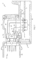
- FIG. 1 is partial cross-sectional view of a power electronic module according to this invention, including a connector, a circuit board and power electronic devices.
- FIG. 2 is an overhead view of the circuit board and power electronic devices of FIG. 1 .
- module 10 generally designates a power electronic module according to this invention.
- module 10 includes a printed circuit board 12 supported within an open-ended metal housing 14, a cover plate 16 fastened to the open end of the housing 14, and a connector assembly 18 that interfaces with circuit board 12 through an opening 20 provided in the top of the housing 14.
- the illustrated connector assembly 18 is a horizontal-mount configuration with four rows of L-shaped pin terminals 22 that enter module 10 substantially parallel to the plane of circuit board 12, and then bend downward 90° to meet circuit board 12 at a right angle.
- the outboard ends of the pin terminals 22 are disposed within a plastic connector shroud 24, while the inboard ends of pin terminals 22 pass through plated through-holes formed 26 in circuit board 12.
- the pin terminals 22 are supported within connector shroud 24 by a pin block 28 and a pin blade stabilizer 30. And prior to entering circuit board 12, the pin terminals 22 pass through a pin alignment fixture 32 keyed to the housing 14 to ensure that the pin terminals 22 are properly aligned with the circuit board through-holes 26.
- the reference numeral 36 designates a power device located outside the region 34 according to conventional practice.
- the present invention recognizes that power devices may be advantageously located within the region 34, as designated for example by the power device 38 in FIG. 1 .
- Locating the power device 38 in the region 34 of circuit board 12 significantly enhances the thermal coupling between device 38 and the pin terminals 22 of connector assembly 18, allowing the pin terminals 22 and any external wiring harness (not shown) coupled to the connector assembly 18 to more effectively dissipate heat generated by the power device 38.
- the thermal coupling is particularly enhanced in the case of leadless power device packages having large copper pads that are soldered to circuit board traces 54 extending from the pin connectors 22. Examples of such power device packages include PQFN, QFN, SO-8, DCA and DPAK.
- FIG. 2 shows the connector region 34 as an outline circumscribing an array of through-holes 26, with the pin terminals 22 removed for ease of illustration, and illustrates several leadless power device packages 40-52 disposed at least partially within the region 34.
- the plated through-holes 26 are each coupled to copper conductor traces 54 formed on the face of circuit board 12, and the device packages 40-52 are soldered to respective conductor traces 54.
- the packages 40-46 are disposed outboard of the plated through-holes 26, while the packages 48-52 are disposed in a space between adjacent rows of plated through-holes 26.
- soldered connections between the device packages and the circuit board traces 54 electrically and thermally couple the device packages 40-52 to respective through-holes 26, to pin terminals 22 inserted in the through-holes 26, and to any wiring harness (not shown) coupled to the pin terminals 22.
- the power device packages 40-52 all contain power transistors such as FETs or IGBTs, although it will be appreciated that other power devices such as power diodes may be used as well or instead.
- the packages 40, 42, 44 and 46 each house a single transistor die 40a, 42a, 44a and 46a; the packages 48 and 50 each house two transistor die 48a, 48b and 50a, 50b; and the package 52 houses four transistor die 52a, 52b, 52c, 52d.
- each of the power device packages 40-52 contains a set of solderable copper leadframe pads 56, 58, 60, 60, 64, 66, one or more semiconductor die 50a, 50b, and a set of wirebonds 68, all overmolded with a plastic encapsulant, although the encapsulant covering the copper pads 56-66, die 50a-50b and wirebonds 68 has been removed for purposes of illustration.
- the exposed bottom-side of each copper leadframe pad 56-66 is soldered to a respective conductor trace 54 of circuit board 12, and the semiconductor die 50a and 50b are soldered to the top-sides of the copper pads 56 and 66 before over-molding.
- Wirebonds 68 electrically couple the top-side terminals of die 50a and 50b to the copper pads 58-64.
- the die 50a can be an IGBT having a bottom-side collector electrode soldered to the copper pad 56, a top-side emitter electrode wire-bonded to the copper pad 60, and a top-side gate electrode wire-bonded to the copper pad 58; where the copper pads 56, 58 and 60 are each soldered to a corresponding copper circuit board trace 54.
- the trace 54 soldered to copper pad 56 (i.e., the IGBT collector) is electrically and thermally coupled to one or more (two in this case) plated through-holes 26 of circuit board 12, while the traces (not shown) soldered to copper pads 58-64 are electrically coupled to buried conductor traces of circuit board 12.
- the present invention provides a practical and cost-effective way of increasing the thermal heat dissipation capability of a power electronic module by more effectively utilizing the thermal heat capacity of connector and wiring harness components.
- locating leadless power electronic devices to utilize the thermal heat capacity of connector and wiring harness components as described herein allows the circuit board and module size to be reduced for a given set of power electronic devices, or alternately, allows the circuit power dissipation to be increased without having to correspondingly increase the circuit board and module size.
- the number of connectors and pin terminals, and the type and number of electronic devices may be different than shown, the pin terminals 22 and through-holes 26 may be arranged in a circular or other pattern, the connector assembly 18 may be a vertical-mount connector design, and so forth.
- a similar arrangement of electronic devices can also be mounted on the underside of circuit board 12. Accordingly, it is intended that the invention not be limited to the disclosed embodiment, but have the full scope permitted by the language of the following claims.
Landscapes
- Engineering & Computer Science (AREA)
- Microelectronics & Electronic Packaging (AREA)
- Cooling Or The Like Of Electrical Apparatus (AREA)
- Structures For Mounting Electric Components On Printed Circuit Boards (AREA)
Applications Claiming Priority (1)
| Application Number | Priority Date | Filing Date | Title |
|---|---|---|---|
| US11/973,518 US20090091889A1 (en) | 2007-10-09 | 2007-10-09 | Power electronic module having improved heat dissipation capability |
Publications (2)
| Publication Number | Publication Date |
|---|---|
| EP2048920A2 true EP2048920A2 (de) | 2009-04-15 |
| EP2048920A3 EP2048920A3 (de) | 2010-01-20 |
Family
ID=40265996
Family Applications (1)
| Application Number | Title | Priority Date | Filing Date |
|---|---|---|---|
| EP08164636A Withdrawn EP2048920A3 (de) | 2007-10-09 | 2008-09-18 | Elektronisches Leistungsmodul mit verbesserter Wärmeableitungsfähigkeit |
Country Status (2)
| Country | Link |
|---|---|
| US (1) | US20090091889A1 (de) |
| EP (1) | EP2048920A3 (de) |
Families Citing this family (3)
| Publication number | Priority date | Publication date | Assignee | Title |
|---|---|---|---|---|
| DE102015106151B4 (de) * | 2015-04-22 | 2019-07-11 | Infineon Technologies Ag | Leiterplatte mit eingebettetem Leistungshalbleiterchip |
| CN110174191A (zh) * | 2019-05-15 | 2019-08-27 | 北京长城华冠汽车科技股份有限公司 | 确定电池模组的发热功率的方法和装置、介质、电子设备 |
| EP4132532A1 (de) * | 2020-04-07 | 2023-02-15 | Laboratoires C.T.R.S. | Topische verwendung von erlotinib zur behandlung von keratoderma bei kindern |
Family Cites Families (66)
| Publication number | Priority date | Publication date | Assignee | Title |
|---|---|---|---|---|
| US4222626A (en) * | 1978-01-16 | 1980-09-16 | Amp Incorporated | Filtered dip header assembly |
| US4401355A (en) * | 1981-07-01 | 1983-08-30 | Rca Corporation | Filtered connector |
| US4600256A (en) * | 1984-12-31 | 1986-07-15 | Motorola, Inc. | Condensed profile electrical connector |
| US4637135A (en) * | 1985-04-01 | 1987-01-20 | Amp Incorporated | Method for mounting a connector to a substrate |
| US4729752A (en) * | 1985-07-26 | 1988-03-08 | Amp Incorporated | Transient suppression device |
| EP0279881B1 (de) * | 1987-02-25 | 1989-09-13 | Winchester Electronics Zweigwerk Der Litton Precision Products International Gmbh | Verfahren und Verbindungsanordnung zum Anschliessen eines mehrpoligen Steckverbinders an eine Leiterplatte |
| FR2620587B1 (fr) * | 1987-09-16 | 1993-07-02 | Telemecanique Electrique | Circuit imprime equipe d'un drain thermique |
| WO1990006609A1 (en) * | 1988-11-16 | 1990-06-14 | Motorola, Inc. | Flexible substrate electronic assembly |
| JP2760829B2 (ja) * | 1989-01-13 | 1998-06-04 | 株式会社日立製作所 | 電子基板 |
| EP0487984B1 (de) * | 1990-11-27 | 1995-06-14 | THOMAS & BETTS CORPORATION | Mit Filter versehener Stiftstecker |
| EP0516149B1 (de) * | 1991-05-31 | 1998-09-23 | Denso Corporation | Elektronische Vorrichtung |
| JP2546590Y2 (ja) * | 1991-05-31 | 1997-09-03 | 日本エー・エム・ピー株式会社 | フィルタコネクタ及びフィルタコネクタ用遮蔽板 |
| JPH06503210A (ja) * | 1991-09-21 | 1994-04-07 | ローベルト ボツシユ ゲゼルシヤフト ミツト ベシユレンクテル ハフツング | 電気装置、特に車両用の切換−及び制御装置 |
| US5218516A (en) * | 1991-10-31 | 1993-06-08 | Northern Telecom Limited | Electronic module |
| WO1993023825A1 (fr) * | 1992-05-20 | 1993-11-25 | Seiko Epson Corporation | Cartouche destinee a un appareil electronique |
| JP2956363B2 (ja) * | 1992-07-24 | 1999-10-04 | 富士電機株式会社 | パワー半導体装置 |
| US5375040A (en) * | 1992-09-29 | 1994-12-20 | Eldec Corporation | Modular electronic circuit housing and wiring board |
| US5415569A (en) * | 1992-10-19 | 1995-05-16 | Molex Incorporated | Filtered electrical connector assembly |
| US5363280A (en) * | 1993-04-22 | 1994-11-08 | International Business Machines Corporation | Printed circuit board or card thermal mass design |
| EP0705183B1 (de) * | 1993-06-26 | 1997-03-05 | Robert Bosch Gmbh | Anbausteuergerät |
| US5519583A (en) * | 1993-12-29 | 1996-05-21 | Storage Technology Corporation | Integrated common mode current decoupler for I/O cables |
| US5802699A (en) * | 1994-06-07 | 1998-09-08 | Tessera, Inc. | Methods of assembling microelectronic assembly with socket for engaging bump leads |
| US5599208A (en) * | 1994-12-14 | 1997-02-04 | The Whitaker Corporation | Electrical connector with printed circuit board programmable filter |
| US5605477A (en) * | 1995-01-13 | 1997-02-25 | The Whitaker Corporation | Flexible etched circuit assembly |
| US5647768A (en) * | 1996-03-11 | 1997-07-15 | General Motors Corporation | Plated plastic filter header |
| JP3315885B2 (ja) * | 1997-01-16 | 2002-08-19 | 株式会社オートネットワーク技術研究所 | コネクタ及びそのコネクタを含む配線装置 |
| US5901044A (en) * | 1997-07-10 | 1999-05-04 | Ilc Data Device Corporation | Mini-module with upwardly directed leads |
| US5933324A (en) * | 1997-12-16 | 1999-08-03 | Intel Corporation | Apparatus for dissipating heat from a conductive layer in a circuit board |
| US6078501A (en) * | 1997-12-22 | 2000-06-20 | Omnirel Llc | Power semiconductor module |
| US6201701B1 (en) * | 1998-03-11 | 2001-03-13 | Kimball International, Inc. | Integrated substrate with enhanced thermal characteristics |
| US6180045B1 (en) * | 1998-05-20 | 2001-01-30 | Delco Electronics Corporation | Method of forming an overmolded electronic assembly |
| JP2000101273A (ja) * | 1998-07-22 | 2000-04-07 | Denso Corp | 電子部品の冷却構造 |
| US6257329B1 (en) * | 1998-08-17 | 2001-07-10 | Alfiero Balzano | Thermal management system |
| US6166464A (en) * | 1998-08-24 | 2000-12-26 | International Rectifier Corp. | Power module |
| JP4234259B2 (ja) * | 1999-05-14 | 2009-03-04 | 富士通テン株式会社 | 電子機器の組合せ構造 |
| US6212071B1 (en) * | 1999-08-20 | 2001-04-03 | Lucent Technologies, Inc. | Electrical circuit board heat dissipation system |
| ES2169687B2 (es) * | 1999-09-30 | 2004-10-16 | Denso Corporation | Unidad electronica de control con elemento de activacion y elemento de tratamiento de control. |
| SE516322C2 (sv) * | 1999-12-01 | 2001-12-17 | Fci Katrineholm Ab | Vinklat kontaktdon samt förfarande för att montera ett sådant |
| US6442027B2 (en) * | 2000-02-23 | 2002-08-27 | Denso Corporation | Electronic control unit having connector positioned between two circuit substrates |
| DE60135405D1 (de) * | 2000-03-21 | 2008-10-02 | Autonetworks Technologies Ltd | Leistungsverteiler für ein Kraftfahrzeug und Verfahren zur Herstellung dazu |
| JP3923703B2 (ja) * | 2000-03-29 | 2007-06-06 | ローム株式会社 | 放熱手段を有するプリント配線板 |
| US6549409B1 (en) * | 2000-08-21 | 2003-04-15 | Vlt Corporation | Power converter assembly |
| JP4151209B2 (ja) * | 2000-08-29 | 2008-09-17 | 三菱電機株式会社 | 電力用半導体装置 |
| US6307749B1 (en) * | 2000-10-23 | 2001-10-23 | Delphi Technologies, Inc. | Overmolded electronic module with underfilled surface-mount components |
| US7046518B2 (en) * | 2001-04-02 | 2006-05-16 | International Rectifier Corporation | Power module |
| JPWO2002082542A1 (ja) * | 2001-04-02 | 2004-07-29 | 三菱電機株式会社 | 電力用半導体装置 |
| JP3988415B2 (ja) * | 2001-07-23 | 2007-10-10 | 住友電装株式会社 | 電気接続箱 |
| US6587346B1 (en) * | 2002-01-31 | 2003-07-01 | Visteon Global Technologies, Inc. | Combination electrical power distribution and heat dissipating device |
| JP3611548B2 (ja) * | 2002-02-20 | 2005-01-19 | Tdk株式会社 | スイッチング電源とその製造方法 |
| US6807731B2 (en) * | 2002-04-02 | 2004-10-26 | Delphi Technologies, Inc. | Method for forming an electronic assembly |
| JP2004063150A (ja) * | 2002-07-25 | 2004-02-26 | Tokai Rika Co Ltd | コネクタ |
| JP3864873B2 (ja) * | 2002-08-09 | 2007-01-10 | 株式会社デンソー | 電子制御装置 |
| US6930885B2 (en) * | 2002-12-23 | 2005-08-16 | Eastman Kodak Company | Densely packed electronic assemblage with heat removing element |
| US6849943B2 (en) * | 2003-06-06 | 2005-02-01 | Electronic Theatre Controls, Inc. | Power module package for high frequency switching system |
| JP2005080370A (ja) * | 2003-08-29 | 2005-03-24 | Auto Network Gijutsu Kenkyusho:Kk | 回路構成体及び防水処理された回路構成体の製造方法 |
| JP2005129274A (ja) * | 2003-10-21 | 2005-05-19 | Fujitsu Ten Ltd | プレスフィット端子および接続構造 |
| JP2005166765A (ja) * | 2003-11-28 | 2005-06-23 | Toshiba Corp | 電子装置および回路モジュール装置 |
| US20060018100A1 (en) * | 2004-07-21 | 2006-01-26 | Yunxing Guo | Active plate-connector device with built-in semiconductor dies |
| JP4322752B2 (ja) * | 2004-08-03 | 2009-09-02 | 株式会社オートネットワーク技術研究所 | 電気接続箱 |
| JP4437958B2 (ja) * | 2004-08-03 | 2010-03-24 | 株式会社オートネットワーク技術研究所 | 電気接続箱 |
| JP4585828B2 (ja) * | 2004-10-06 | 2010-11-24 | 日立オートモティブシステムズ株式会社 | 制御装置およびその製造方法 |
| US7190589B2 (en) * | 2004-10-19 | 2007-03-13 | Cinch Connectors, Inc. | Electronic control enclosure |
| US7473585B2 (en) * | 2005-06-13 | 2009-01-06 | Delphi Technologies, Inc. | Technique for manufacturing an overmolded electronic assembly |
| US7209360B1 (en) * | 2005-10-28 | 2007-04-24 | Lear Corporation | Leak-tight system for boxes containing electrical and electronic components |
| JP4582002B2 (ja) * | 2006-01-10 | 2010-11-17 | 株式会社デンソー | 電子装置 |
| JP4736903B2 (ja) * | 2006-03-31 | 2011-07-27 | 株式会社ジェイテクト | 電子制御装置 |
-
2007
- 2007-10-09 US US11/973,518 patent/US20090091889A1/en not_active Abandoned
-
2008
- 2008-09-18 EP EP08164636A patent/EP2048920A3/de not_active Withdrawn
Also Published As
| Publication number | Publication date |
|---|---|
| US20090091889A1 (en) | 2009-04-09 |
| EP2048920A3 (de) | 2010-01-20 |
Similar Documents
| Publication | Publication Date | Title |
|---|---|---|
| US9209114B2 (en) | Power module package with a fastening unit including a non-conductive portion | |
| US9202798B2 (en) | Power module package and method for manufacturing the same | |
| US9230891B2 (en) | Semiconductor device | |
| US10681801B2 (en) | Mounting assembly with a heatsink | |
| US20140167237A1 (en) | Power module package | |
| CN109817590B (zh) | 半导体装置 | |
| US20140110833A1 (en) | Power module package | |
| JP2002184933A (ja) | 半導体装置 | |
| CN112864113A (zh) | 功率器件、功率器件组件与相关装置 | |
| US20120241934A1 (en) | Semiconductor apparatus and method for manufacturing the same | |
| JP2006505945A (ja) | 折返しフレックス・無ワイヤボンディング・マルチチップ電力パッケージ | |
| KR20190095998A (ko) | 전력용 반도체 모듈 | |
| US6396699B1 (en) | Heat sink with chip die EMC ground interconnect | |
| CN215008199U (zh) | 功率器件、功率器件组件、电能转换装置及电能转换设备 | |
| EP2048920A2 (de) | Elektronisches Leistungsmodul mit verbesserter Wärmeableitungsfähigkeit | |
| KR100598652B1 (ko) | 반도체장치 | |
| US20070257377A1 (en) | Package structure | |
| CN109801900B (zh) | 一种电力用逆变电路装置 | |
| US7310224B2 (en) | Electronic apparatus with thermal module | |
| EP4283670A2 (de) | Geformte leistungsmodule | |
| US9129948B2 (en) | Semiconductor device and method of assembling same | |
| CN116598265A (zh) | 一种系统级封装sip模块及其组装方法 | |
| JP5120087B2 (ja) | 半導体装置及びその製造方法 | |
| KR102843819B1 (ko) | 인쇄 회로 기판을 이용한 내부 연결 구조를 갖는 파워 모듈 | |
| US20230028579A1 (en) | Semiconductor device and a method of manufacturing of a semiconductor device |
Legal Events
| Date | Code | Title | Description |
|---|---|---|---|
| PUAI | Public reference made under article 153(3) epc to a published international application that has entered the european phase |
Free format text: ORIGINAL CODE: 0009012 |
|
| AK | Designated contracting states |
Kind code of ref document: A2 Designated state(s): AT BE BG CH CY CZ DE DK EE ES FI FR GB GR HR HU IE IS IT LI LT LU LV MC MT NL NO PL PT RO SE SI SK TR |
|
| AX | Request for extension of the european patent |
Extension state: AL BA MK RS |
|
| PUAL | Search report despatched |
Free format text: ORIGINAL CODE: 0009013 |
|
| AK | Designated contracting states |
Kind code of ref document: A3 Designated state(s): AT BE BG CH CY CZ DE DK EE ES FI FR GB GR HR HU IE IS IT LI LT LU LV MC MT NL NO PL PT RO SE SI SK TR |
|
| AX | Request for extension of the european patent |
Extension state: AL BA MK RS |
|
| 17P | Request for examination filed |
Effective date: 20100720 |
|
| AKX | Designation fees paid |
Designated state(s): AT BE BG CH CY CZ DE DK EE ES FI FR GB GR HR HU IE IS IT LI LT LU LV MC MT NL NO PL PT RO SE SI SK TR |
|
| 17Q | First examination report despatched |
Effective date: 20101013 |
|
| STAA | Information on the status of an ep patent application or granted ep patent |
Free format text: STATUS: THE APPLICATION IS DEEMED TO BE WITHDRAWN |
|
| 18D | Application deemed to be withdrawn |
Effective date: 20110224 |