EP0487984B1 - Mit Filter versehener Stiftstecker - Google Patents
Mit Filter versehener Stiftstecker Download PDFInfo
- Publication number
- EP0487984B1 EP0487984B1 EP91119414A EP91119414A EP0487984B1 EP 0487984 B1 EP0487984 B1 EP 0487984B1 EP 91119414 A EP91119414 A EP 91119414A EP 91119414 A EP91119414 A EP 91119414A EP 0487984 B1 EP0487984 B1 EP 0487984B1
- Authority
- EP
- European Patent Office
- Prior art keywords
- plate
- housing
- capacitor
- ground plate
- filtered
- Prior art date
- Legal status (The legal status is an assumption and is not a legal conclusion. Google has not performed a legal analysis and makes no representation as to the accuracy of the status listed.)
- Expired - Lifetime
Links
Images
Classifications
-
- H—ELECTRICITY
- H01—ELECTRIC ELEMENTS
- H01R—ELECTRICALLY-CONDUCTIVE CONNECTIONS; STRUCTURAL ASSOCIATIONS OF A PLURALITY OF MUTUALLY-INSULATED ELECTRICAL CONNECTING ELEMENTS; COUPLING DEVICES; CURRENT COLLECTORS
- H01R13/00—Details of coupling devices of the kinds covered by groups H01R12/70 or H01R24/00 - H01R33/00
- H01R13/66—Structural association with built-in electrical component
- H01R13/719—Structural association with built-in electrical component specially adapted for high frequency, e.g. with filters
- H01R13/7195—Structural association with built-in electrical component specially adapted for high frequency, e.g. with filters with planar filters with openings for contacts
-
- H—ELECTRICITY
- H01—ELECTRIC ELEMENTS
- H01R—ELECTRICALLY-CONDUCTIVE CONNECTIONS; STRUCTURAL ASSOCIATIONS OF A PLURALITY OF MUTUALLY-INSULATED ELECTRICAL CONNECTING ELEMENTS; COUPLING DEVICES; CURRENT COLLECTORS
- H01R12/00—Structural associations of a plurality of mutually-insulated electrical connecting elements, specially adapted for printed circuits, e.g. printed circuit boards [PCB], flat or ribbon cables, or like generally planar structures, e.g. terminal strips, terminal blocks; Coupling devices specially adapted for printed circuits, flat or ribbon cables, or like generally planar structures; Terminals specially adapted for contact with, or insertion into, printed circuits, flat or ribbon cables, or like generally planar structures
- H01R12/70—Coupling devices
- H01R12/71—Coupling devices for rigid printing circuits or like structures
- H01R12/72—Coupling devices for rigid printing circuits or like structures coupling with the edge of the rigid printed circuits or like structures
- H01R12/722—Coupling devices for rigid printing circuits or like structures coupling with the edge of the rigid printed circuits or like structures coupling devices mounted on the edge of the printed circuits
- H01R12/724—Coupling devices for rigid printing circuits or like structures coupling with the edge of the rigid printed circuits or like structures coupling devices mounted on the edge of the printed circuits containing contact members forming a right angle
Definitions
- the invention relates to an electrical connector and, in particular to a filtered plug connector of the type including a housing having a plurality of bores through which a respective plurality of plug pins pass, a ground plate supported by said housing and a plurality of multi-layer capacitors of the type comprising a pair of spaced external electrodes, one electrode of each capacitor being in engagement with a respective plug pin and the other electrode of each capacitor being in engagement with the ground plate, said ground plate comprising a resilient portion projecting outwardly from the ground plate for each capacitor, each said resilient portion resiliently engaging one of said capacitor electrodes and pressing said capacitor toward said plug pin to thereby cause engagement of said other capacitor electrode with said plug pin.
- Filtered plug connectors of this specific type are known from US-A-4,582,385.
- Filtered plug connectors of this type serve for connecting printed circuit boards to other electrical components.
- the plug pins thereof are inserted with their one ends into the metallized holes in the printed circuit board. Their other ends extend for example to the wires of a cable.
- high-frequency signals or interference signals are to be removed.
- the multi-layer ceramic capacitors which are disposed between a ground plate and the plug pins are provided for that purpose. The capacitors are of dimensions of only a very few millimeters and they are arranged on a printed circuit board which is fixed in the plug.
- the ceramic capacitors are resiliently mounted between the resilient portions projecting outwardly from the ground plate on the one hand and the plug pins on the other hand. Therefore, the ceramic capacitors are no longer fixedly fastened to a circuit board and there is less risk of damage to the capacitors by fast movements, vibrations or shocks as it may happen with the plug connectors as referred to in the second paragraph of this specification, keeping in mind that the ceramic capacitors are rather brittle.
- a filtered plug connector in which the ceramic capacitors are retained in position more firmly to provide higher mechanical stability while maintaining resiliency as a safety means against vibrations and shock.
- the solution to this objective is achieved in a filtered plug connector of the kind as set forth in the first paragraph of this specification, in accordance with the invention, in that a plate is supported by and holds said capacitors against said housing in a non-rigid manner, and in that the resilient portions of said ground plate press the capacitors between the housing and plate against the respective plug pins.
- the elasticity of the ground plate and in particular of the resilient portions thereof is considered sufficient to clamp the multi-layer ceramic capacitors in position resiliently and nonetheless securely assisted by the plate according to the invention.
- the capacitors are sufficiently securely held in place from the mechanical point of view.
- the pressure applied by the ground plate is also sufficient to provide a sound electrical connection.
- the manner in which the multi-layer ceramic capacitors are held in position between the plug pins on one side and the ground plate on the other side is not rigid. As such, the multi-layer ceramic capacitors do not follow all possible movements, and as a result they are not subjected to a mechanical loading and the risk of breakage is reduced.
- a desirable configuration provides that the openings in the ground plate are surrounded by plate portions which are bent out of the ground plate towards the housing.
- the height of such plate portions corresponds at least to the thickness of the multi-layer ceramic capacitors, and the latter are clamped between the plate portions and the plug pins.
- the plate portions have a flat section extending parallel to the end faces of the multi-layer ceramic capacitors. The length of the plate portions approximately corresponds to the height or thickness of the multi-layer ceramic capacitors. The flat section bears against the end faces or metallized ends of the multi-layer ceramic capacitors.
- a further desirable configuration provides that disposed on the inside of the housing are recesses and the plate portions are bent into said recesses.
- a plate lies on the ground plate, the plate having protrusions which are aligned with the openings in the ground plate and the multi-layer ceramic capacitors and bearing against the capacitors. The protrusions of the plate additionally fix the multi-layer ceramic capacitors. Likewise they additionally fix the ground plate.
- the multi-layer ceramic capacitors may be arranged on one or both sides of the plug pins.
- the housing When a multi-layer ceramic capacitor is disposed only on one side of the plug pin, desirably, at the side of the plug pin which is remote from the multi-layer ceramic capacitor, the housing has a support which bears against the plug pin. In addition at the side of the multi-layer ceramic capacitor which is remote from the protrusion of the plate, the housing may have a support which bears against the capacitor.
- the supports are formed integrally with the housing. The first-mentioned support bears against a plug pin and the additionally mentioned support bears against a multi-layer ceramic capacitor. By virtue of that arrangement those components are additionally supported and fixed in position.
- plugs may also be soldered with one of their metallized ends to a plug pin and with their other metallized end to the inwardly bent plate portions of the ground plate.
- the plugs are exposed to shocks, shaking movements and/or vibration.
- an embodiment is recommended in accordance with the invention in which depressions are provided on the inside of the housing to receive the multi-layer ceramic capacitors and the latter are disposed in the depressions.
- the dimensions of the depressions are so matched to those of the multi-layer ceramic capacitors that they are positively held in the depressions.
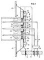
- Figure 1 is a partly sectional side view of a first embodiment of a plug connector.
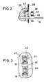
- Figure 2 is a partly sectional side view of a second embodiment illustrating the depression accommodating a multi-layer ceramic capacitor
- Figure 3 is a view taken along line III-III in Figure 1.
- Figure 1 shows a part of a printed circuit board 12 with metallized holes 14. Plug pins 16 are fitted into the latter. Some of the plug pins 16 are held together and fixed with a plate portion 18.
- FIG 1 shows the housing 20, insofar as is essential for the present invention. Bores 22 pass through the housing 20 and accommodate the plug pins 16.
- a plate 26 lies on the inside 24 of the housing 20, with the interposition of the ground plate which is to be described hereinafter.
- the plate 26 has protrusions 28. The protrusions 28 bear against the multi-layer ceramic capacitors which are to be described hereinafter.
- Figure 1 also shows rivet heads 30 which are formed integrally with the housing 20. They pass through openings in the plate 26 and fix the plate 26 to the housing 20.
- Figure 1 shows three plug pins 16.
- the multi-layer ceramic capacitors to be described hereinafter are disposed only at the top side thereof.
- the multi-layer ceramic capacitors are disposed on both sides thereof.
- the housing 20 has supports 32 which are formed integrally therewith. The supports 32 engage under and fix the plug pins 16. In that way the pins are protected from being bent.
- the housing further has supports or protuberances 34.
- the supports 34 are also formed integrally with the housing 20 and bear against the left-hand side of the multi-layer ceramic capacitors. In that way the capacitors are fixed in a lateral direction between the protrusions 28 and the supports 34.
- a ground plate 36 lies on the inward side 24 of the housing 20.
- a front plate 40 is disposed on the other side of the housing 20.
- a ground conductor 38 which is connected to the ground plate 36 is inserted into a metallised hole 14.
- the ground plate 36 also bears with resilient ends against the inward side of the front plate 40.
- the ground plate 36 has openings surrounding the plug pins 16.
- the openings have plate portions 42 which are bent out towards the left, when looking at Figure 1.
- the plate portions include flat sections which lie against an end of the above-mentioned multi-layer ceramic capacitors 44.
- the multi-layer ceramic capacitors 44 are respectively disposed between a plug pin 16 and a plate portion 42. In that arrangement, a respective multi-layer ceramic capacitor bears against each of the two upper plug pins 16 while two such capacitors bear against the lower plug pin 16.
- the multi-layer ceramic capacitors 44 have metallized ends 46. They can be soldered to the plug pins 16 and the outwardly bent plate portions 42, thereby providing solder locations 46.
- FIG 2 As shown in Figure 2, provided in the inward side of the housing 20 are depressions 50. The dimensions thereof are practically identical to those of a multi-layer ceramic capacitor 42. Each capacitor is pressed into a depression 50 in the direction of the arrow shown i Figure 2 and then positively held therein.
- Figure 3 shows a region from Figure 1.
- multi-layer ceramic capacitors 44 each bear from above against a plug pin 16, by way of one of their metallized ends 46.
Claims (12)
- Ein mit einem Filter versehener Steckerverbinder der Bauart mit einem Gehäuse (20) mit einer Vielzahl von Bohrungen (22), durch die eine entsprechende Vielzahl von Stekkerstiften (16) durchtritt, mit einem von dem Gehäuse (20) getragenen Masseblech (36) und mit einer Vielzahl von Vielschichtkondensatoren (44) der Bauart mit zwei auseinanderliegenden Außenelektroden, wobei eine Elektrode (46) jedes Kondensators (44) an dem jeweiligen Stekkerstift (16) und die andere Elektrode (46) jedes Kondensators (44) an dem Masseblech (36) anliegt, das Masseblech (36) für jeden Kondensator (44) einen von ihm nach außen vorspringenden federnden Abschnitt (42) umfaßt, jeder federnde Abschnitt (42) an einer der Kondensatorelektroden (46) federnd anliegt und den Kondensator (44) in Richtung auf den Steckerstift (16) drückt, um damit eine Anlage der anderen Kondensatorelektrode (46) am Steckerstift (16) zu erreichen, dadurch gekennzeichnet, daß eine Platte (26) von den Kondensatoren (44) abgestützt wird und diese in einer nicht-starren Weise am Gehäuse (20) hält und daß die federnden Abschnitte (42) des Massebleches (36) die Kondensatoren (44) zwischen dem Gehäuse (20) und der Platte (26) gegen die jeweiligen Steckerstifte (16) drücken.
- Ein mit einem Filter versehener Steckerverbinder nach Anspruch 1, dadurch gekennzeichnet, daß das Masseblech (36) eine Vielzahl von Öffnungen aufweist, durch die die entsprechende Vielzahl der Stifte verläuft, und das Masseblech (36) zwischen dem Gehäuse (20) und der Platte (26) liegt.
- Ein mit einem Filter versehener Steckerverbinder nach Anspruch 2, dadurch gekennzeichnet, daß die Platte (26) am Gehäuse (20) befestigt ist.
- Ein mit einem Filter versehener Steckerverbinder nach Anspruch 3, dadurch gekennzeichnet, daß die Stifte (16) unter Ausbildung einer Längsachse im allgemeinen langgestreckt sind, die Vielschichtkondensatoren (44) eine parallelepipedische Gestalt haben und zwischen dem Gehäuse (20) und dem Blech (36) in einer Richtung im allgemeinen quer zu der Achse eines betreffenden Stiftes (16) abgestützt werden, das Gehäuse (20) und die Platte (36) an jedem Kondensator (44) auf gegenüberliegenden Oberflächen von diesem anliegen und eine Bewegung jedes Kondensators (44) in einer Richtung entlang der Stiftachse im wesentlichen verhindern und daß der federnde Abschnitt (42) des Massebleches für ein federndes Klemmen des Kondensators am Stift (16) in einer Richtung quer zu jeder Stiftachse sorgt.
- Ein mit einem Filter versehener Steckerverbinder nach Anspruch 4, dadurch gekennzeichnet, daß die federnden Abschnitte (42) an den jeweiligen Öffnungen im Masseblech (36) liegen und aus dem Masseblech (36) in Richtung auf das Gehäuse (20) weggebogen sind.
- Ein mit einem Filter versehener Steckerverbinder nach Anspruch 5, dadurch gekennzeichnet, daß Aussparungen auf der Innenseite (24) des Gehäuses (20) vorgesehen und die Blechabschnitte (42) in die Aussparungen hineingebogen sind.
- Ein mit einem Filter versehener Steckerverbinder nach Anspruch 4, dadurch gekennzeichnet, daß die Platte (26) Auswölbungen (28) aufweist, die mit den Öffnungen im Masseblech (36) ausgerichtet sind und in diese hinein verlaufen und an einer Oberfläche der Vielschichtkondensatoren (44) anliegen.
- Ein mit einem Filter versehener Steckerverbinder nach Anspruch 7, dadurch gekennzeichnet, daß das Gehäuse (20) an der von der Vorwölbung (28) der Platte (26) abgelegenen Seite des Vielschichtkeramik-Kondensators (44) ein an diesem anliegendes Auflager (34) aufweist.
- Ein mit einem Filter versehener Steckerverbinder nach Anspruch 4, dadurch gekennzeichnet, daß das Gehäuse 820) an der von dem Vielschichtkeramik-Kondensator (44) abgelegenen Seite des Steckerstiftes (16) ein an diesem anliegendes Auflager (32) aufweist.
- Ein mit einem Filter versehener Steckerverbinder nach Anspruch 4, dadurch gekennzeichnet, daß auf der Innenseite (24) des Gehäuses (20) die Vielschichtkeramik-Kondensatoren (44) aufnehmende Vertiefungen (50) vorgesehen sind.
- Ein mit einem Filter versehener Steckerverbinder nach Anspruch 1, dadurch gekennzeichnet, daß die Vielschichtkeramik-Kondensatoren (44) mit einer metallisierten Elektrode (46) an die Steckerstifte (16) angelötet sind.
- Ein mit einem Filter versehener Steckerverbinder nach Anspruch 11, dadurch gekennzeichnet, daß die Vielschichtkeramik-Kondensatoren (44) mit einer anderen metallisierten Elektrode (46) an die Plattenabschnitte (42) des Massebleches (36) angelötet sind.
Applications Claiming Priority (2)
| Application Number | Priority Date | Filing Date | Title |
|---|---|---|---|
| DE4037602 | 1990-11-27 | ||
| DE4037602 | 1990-11-27 |
Publications (3)
| Publication Number | Publication Date |
|---|---|
| EP0487984A2 EP0487984A2 (de) | 1992-06-03 |
| EP0487984A3 EP0487984A3 (en) | 1992-07-22 |
| EP0487984B1 true EP0487984B1 (de) | 1995-06-14 |
Family
ID=6418948
Family Applications (1)
| Application Number | Title | Priority Date | Filing Date |
|---|---|---|---|
| EP91119414A Expired - Lifetime EP0487984B1 (de) | 1990-11-27 | 1991-11-14 | Mit Filter versehener Stiftstecker |
Country Status (6)
| Country | Link |
|---|---|
| US (1) | US5152699A (de) |
| EP (1) | EP0487984B1 (de) |
| JP (1) | JPH0777140B2 (de) |
| AU (1) | AU641061B2 (de) |
| CA (1) | CA2056339C (de) |
| DE (1) | DE69110418T2 (de) |
Cited By (1)
| Publication number | Priority date | Publication date | Assignee | Title |
|---|---|---|---|---|
| DE19611699C1 (de) * | 1996-03-25 | 1997-11-13 | Siemens Ag | Filter-Steckverbinder mit Abschirmgehäuse |
Families Citing this family (33)
| Publication number | Priority date | Publication date | Assignee | Title |
|---|---|---|---|---|
| DE9208702U1 (de) * | 1992-06-29 | 1993-10-28 | Siemens Ag | Filter-Steckverbinder mit Schirmgehäuse |
| US5498180A (en) * | 1992-10-05 | 1996-03-12 | Amphenol Corporation | Diode/filter connector |
| DE4339653A1 (de) * | 1992-12-04 | 1994-06-09 | Fichtel & Sachs Ag | Anschlußvorrichtung für eine von einer elektrisch leitenden Wandung eines Gehäuses abgeschirmte, elektrische Anordnung |
| GB2273210B (en) * | 1992-12-04 | 1996-08-07 | Fichtel & Sachs Ag | Connection device for an electrical arrangement shielded by an electrically conductive wall of a housing |
| US5266054A (en) * | 1992-12-22 | 1993-11-30 | The Whitaker Corporation | Sealed and filtered header receptacle |
| DE4412173A1 (de) * | 1993-04-08 | 1994-10-13 | Amphenol Tuchel Elect | Rundsteckverbinder mit Filter |
| US5286224A (en) * | 1993-05-10 | 1994-02-15 | Itt Corporation | Interchangeable contact connector |
| US5340334A (en) * | 1993-07-19 | 1994-08-23 | The Whitaker Corporation | Filtered electrical connector |
| US5399099A (en) * | 1993-08-12 | 1995-03-21 | The Whitaker Corporation | EMI protected tap connector |
| US5599208A (en) * | 1994-12-14 | 1997-02-04 | The Whitaker Corporation | Electrical connector with printed circuit board programmable filter |
| US5562499A (en) * | 1995-01-30 | 1996-10-08 | Stanley E. Gately | Multiposition electrical connector filter adapter |
| EP1037328B1 (de) * | 1995-02-07 | 2003-10-22 | Johnstech International Corporation | Gerät zur Steuerung der Impedanz von elektrischen Kontakten |
| US5554050A (en) * | 1995-03-09 | 1996-09-10 | The Whitaker Corporation | Filtering insert for electrical connectors |
| US5580280A (en) * | 1995-06-30 | 1996-12-03 | The Whitaker Corporation | Filtered electrical connector |
| US5624277A (en) * | 1995-08-28 | 1997-04-29 | The Whitaker Corporation | Filtered and shielded electrical connector using resilient electrically conductive member |
| US6033263A (en) * | 1996-10-15 | 2000-03-07 | The Whitaker Corporation | Electrically connector with capacitive coupling |
| US5865648A (en) * | 1997-01-16 | 1999-02-02 | Elco U.S.A. Inc. | Multifunction electronic connector |
| US5975958A (en) * | 1997-10-14 | 1999-11-02 | The Whitaker Corporation | Capactive coupling adapter for an electrical connector |
| US6007351A (en) * | 1998-07-23 | 1999-12-28 | Packard Hughes Interconnect Company | Bussplate |
| US6142831A (en) * | 1999-02-01 | 2000-11-07 | Aux Corporation | Multifunction connector assembly |
| US6858793B1 (en) * | 1999-09-09 | 2005-02-22 | Koninklijke Philips Electronics N.V. | EMI-suppression plate for use in IEEE-1394 applications |
| DE10233318C1 (de) * | 2002-07-22 | 2003-09-25 | Siemens Ag | Entstöreinrichtung |
| US20040085158A1 (en) * | 2002-10-23 | 2004-05-06 | Van Hoyweghen Joseph V. | Dielectric component array |
| US7295086B2 (en) * | 2002-10-23 | 2007-11-13 | Spectrum Control Inc. | Dielectric component array with failsafe link |
| US6837747B1 (en) | 2004-04-19 | 2005-01-04 | Itt Manufacturing Enterprises, Inc. | Filtered connector |
| US7361055B2 (en) * | 2005-01-14 | 2008-04-22 | Molex Incorporated | Modular filter connector |
| US7442085B2 (en) * | 2005-01-14 | 2008-10-28 | Molex Incorporated | Filter connector |
| US20090091889A1 (en) * | 2007-10-09 | 2009-04-09 | Oman Todd P | Power electronic module having improved heat dissipation capability |
| ITVI20080063A1 (it) * | 2008-03-12 | 2009-09-13 | Sumoto Srl | Struttura di connettore di alimentazione. |
| US8241067B2 (en) * | 2009-11-04 | 2012-08-14 | Amphenol Corporation | Surface mount footprint in-line capacitance |
| CN102854939B (zh) * | 2011-06-30 | 2017-06-06 | 赛恩倍吉科技顾问(深圳)有限公司 | I/o端口组合 |
| US9831588B2 (en) * | 2012-08-22 | 2017-11-28 | Amphenol Corporation | High-frequency electrical connector |
| CN105792515A (zh) * | 2014-12-25 | 2016-07-20 | 台达电子工业股份有限公司 | 电路板组合及其组装方法 |
Family Cites Families (9)
| Publication number | Priority date | Publication date | Assignee | Title |
|---|---|---|---|---|
| US4500159A (en) * | 1983-08-31 | 1985-02-19 | Allied Corporation | Filter electrical connector |
| US4582385A (en) * | 1983-10-31 | 1986-04-15 | International Telephone & Telegraph Corp. | Electrical connector embodying electrical circuit components |
| US4690479A (en) * | 1985-10-10 | 1987-09-01 | Amp Incorporated | Filtered electrical header assembly |
| US4707048A (en) * | 1986-11-03 | 1987-11-17 | Amphenol Corporation | Electrical connector having means for protecting terminals from transient voltages |
| JPS63165786U (de) * | 1987-04-16 | 1988-10-28 | ||
| DE8902245U1 (de) * | 1989-02-25 | 1989-05-11 | Thomas & Betts Corp., Bridgewater, N.J., Us | |
| US4950185A (en) * | 1989-05-18 | 1990-08-21 | Amphenol Corporation | Stress isolated planar filter design |
| US4930200A (en) * | 1989-07-28 | 1990-06-05 | Thomas & Betts Corporation | Method of making an electrical filter connector |
| US5057041A (en) * | 1990-06-29 | 1991-10-15 | Foxconn International | User configurable integrated electrical connector assembly |
-
1991
- 1991-11-14 EP EP91119414A patent/EP0487984B1/de not_active Expired - Lifetime
- 1991-11-14 DE DE69110418T patent/DE69110418T2/de not_active Expired - Fee Related
- 1991-11-19 AU AU87959/91A patent/AU641061B2/en not_active Ceased
- 1991-11-21 US US07/796,563 patent/US5152699A/en not_active Expired - Lifetime
- 1991-11-27 CA CA002056339A patent/CA2056339C/en not_active Expired - Fee Related
- 1991-11-27 JP JP3312507A patent/JPH0777140B2/ja not_active Expired - Lifetime
Cited By (1)
| Publication number | Priority date | Publication date | Assignee | Title |
|---|---|---|---|---|
| DE19611699C1 (de) * | 1996-03-25 | 1997-11-13 | Siemens Ag | Filter-Steckverbinder mit Abschirmgehäuse |
Also Published As
| Publication number | Publication date |
|---|---|
| DE69110418D1 (de) | 1995-07-20 |
| AU641061B2 (en) | 1993-09-09 |
| JPH04267085A (ja) | 1992-09-22 |
| EP0487984A3 (en) | 1992-07-22 |
| EP0487984A2 (de) | 1992-06-03 |
| DE69110418T2 (de) | 1996-03-07 |
| CA2056339C (en) | 1995-03-21 |
| JPH0777140B2 (ja) | 1995-08-16 |
| AU8795991A (en) | 1992-06-18 |
| CA2056339A1 (en) | 1992-05-28 |
| US5152699A (en) | 1992-10-06 |
Similar Documents
| Publication | Publication Date | Title |
|---|---|---|
| EP0487984B1 (de) | Mit Filter versehener Stiftstecker | |
| KR910001318B1 (ko) | 전화 잭 | |
| US7252552B2 (en) | Connector having an electronic element built therein without disturbing a characteristic impedance | |
| US5239748A (en) | Method of making high density connector for burn-in boards | |
| US3501582A (en) | Electrical assembly | |
| CA2245965C (en) | Miniature card edge clip | |
| US5624277A (en) | Filtered and shielded electrical connector using resilient electrically conductive member | |
| US4784618A (en) | Filter connector device | |
| EP0299563A1 (de) | Filtereinheit für Verbinder | |
| EP0835536B1 (de) | Elektrischer verbinder mit filter | |
| EP0430105A1 (de) | Steckdose für mehrpoligen Verbinder | |
| JPH0676894A (ja) | コネクタ | |
| KR0122783Y1 (ko) | 인쇄 회로 기판용 연부 접속기 | |
| US5123851A (en) | Integrated connector module with conductive elastomeric contacts | |
| US6743047B2 (en) | Electrical connector with rear ground plate | |
| US4629267A (en) | Circuit terminating device | |
| JP3453631B2 (ja) | コネクタ及びその製造・実装方法 | |
| EP0724312B1 (de) | Elektrischer Verbinder mit Mehrstellungsfilteradapter | |
| EP0643448A1 (de) | Koaxialverbinder zur Verbindung mit Leiterplatten | |
| US6116925A (en) | Stacked electrical card connector | |
| US6506079B1 (en) | Multi-pole angle-connecting device | |
| US5364293A (en) | Shielded stackable solderless connector/filter assembly | |
| JPH0514469Y2 (de) | ||
| JP3212302B1 (ja) | 抵抗アレーボード | |
| JPS5848498A (ja) | 電気部品ユニツト |
Legal Events
| Date | Code | Title | Description |
|---|---|---|---|
| PUAI | Public reference made under article 153(3) epc to a published international application that has entered the european phase |
Free format text: ORIGINAL CODE: 0009012 |
|
| PUAL | Search report despatched |
Free format text: ORIGINAL CODE: 0009013 |
|
| AK | Designated contracting states |
Kind code of ref document: A2 Designated state(s): BE CH DE ES FR GB IT LI LU NL SE |
|
| AK | Designated contracting states |
Kind code of ref document: A3 Designated state(s): BE CH DE ES FR GB IT LI LU NL SE |
|
| 17P | Request for examination filed |
Effective date: 19930118 |
|
| RAP3 | Party data changed (applicant data changed or rights of an application transferred) |
Owner name: THOMAS & BETTS CORPORATION |
|
| 17Q | First examination report despatched |
Effective date: 19940628 |
|
| GRAA | (expected) grant |
Free format text: ORIGINAL CODE: 0009210 |
|
| AK | Designated contracting states |
Kind code of ref document: B1 Designated state(s): BE CH DE ES FR GB IT LI LU NL SE |
|
| PG25 | Lapsed in a contracting state [announced via postgrant information from national office to epo] |
Ref country code: IT Free format text: LAPSE BECAUSE OF FAILURE TO SUBMIT A TRANSLATION OF THE DESCRIPTION OR TO PAY THE FEE WITHIN THE PRESCRIBED TIME-LIMIT;WARNING: LAPSES OF ITALIAN PATENTS WITH EFFECTIVE DATE BEFORE 2007 MAY HAVE OCCURRED AT ANY TIME BEFORE 2007. THE CORRECT EFFECTIVE DATE MAY BE DIFFERENT FROM THE ONE RECORDED. Effective date: 19950614 Ref country code: LI Effective date: 19950614 Ref country code: BE Effective date: 19950614 Ref country code: ES Free format text: THE PATENT HAS BEEN ANNULLED BY A DECISION OF A NATIONAL AUTHORITY Effective date: 19950614 Ref country code: CH Effective date: 19950614 Ref country code: FR Effective date: 19950614 Ref country code: NL Free format text: LAPSE BECAUSE OF NON-PAYMENT OF DUE FEES Effective date: 19950614 |
|
| REF | Corresponds to: |
Ref document number: 69110418 Country of ref document: DE Date of ref document: 19950720 |
|
| PG25 | Lapsed in a contracting state [announced via postgrant information from national office to epo] |
Ref country code: SE Effective date: 19950914 |
|
| REG | Reference to a national code |
Ref country code: CH Ref legal event code: PL |
|
| EN | Fr: translation not filed | ||
| PG25 | Lapsed in a contracting state [announced via postgrant information from national office to epo] |
Ref country code: LU Free format text: LAPSE BECAUSE OF NON-PAYMENT OF DUE FEES Effective date: 19951130 |
|
| NLV1 | Nl: lapsed or annulled due to failure to fulfill the requirements of art. 29p and 29m of the patents act | ||
| PLBE | No opposition filed within time limit |
Free format text: ORIGINAL CODE: 0009261 |
|
| STAA | Information on the status of an ep patent application or granted ep patent |
Free format text: STATUS: NO OPPOSITION FILED WITHIN TIME LIMIT |
|
| 26N | No opposition filed | ||
| REG | Reference to a national code |
Ref country code: GB Ref legal event code: IF02 |
|
| PGFP | Annual fee paid to national office [announced via postgrant information from national office to epo] |
Ref country code: GB Payment date: 20071128 Year of fee payment: 17 |
|
| PGFP | Annual fee paid to national office [announced via postgrant information from national office to epo] |
Ref country code: DE Payment date: 20071221 Year of fee payment: 17 |
|
| GBPC | Gb: european patent ceased through non-payment of renewal fee |
Effective date: 20081114 |
|
| PG25 | Lapsed in a contracting state [announced via postgrant information from national office to epo] |
Ref country code: DE Free format text: LAPSE BECAUSE OF NON-PAYMENT OF DUE FEES Effective date: 20090603 |
|
| PG25 | Lapsed in a contracting state [announced via postgrant information from national office to epo] |
Ref country code: GB Free format text: LAPSE BECAUSE OF NON-PAYMENT OF DUE FEES Effective date: 20081114 |