EP2043191A1 - Module de cellule solaire sensible aux colorants et procédé de fabrication correspondant - Google Patents
Module de cellule solaire sensible aux colorants et procédé de fabrication correspondant Download PDFInfo
- Publication number
- EP2043191A1 EP2043191A1 EP07768092A EP07768092A EP2043191A1 EP 2043191 A1 EP2043191 A1 EP 2043191A1 EP 07768092 A EP07768092 A EP 07768092A EP 07768092 A EP07768092 A EP 07768092A EP 2043191 A1 EP2043191 A1 EP 2043191A1
- Authority
- EP
- European Patent Office
- Prior art keywords
- layer
- insulating layer
- substrates
- dye
- solar cell
- Prior art date
- Legal status (The legal status is an assumption and is not a legal conclusion. Google has not performed a legal analysis and makes no representation as to the accuracy of the status listed.)
- Granted
Links
- 238000000034 method Methods 0.000 title claims description 58
- 239000000758 substrate Substances 0.000 claims abstract description 273
- 239000004065 semiconductor Substances 0.000 claims abstract description 151
- 239000003054 catalyst Substances 0.000 claims abstract description 105
- 238000006243 chemical reaction Methods 0.000 claims abstract description 93
- 239000003792 electrolyte Substances 0.000 claims abstract description 44
- 239000000463 material Substances 0.000 claims description 113
- 229920005989 resin Polymers 0.000 claims description 81
- 239000011347 resin Substances 0.000 claims description 81
- 238000004519 manufacturing process Methods 0.000 claims description 29
- 239000008151 electrolyte solution Substances 0.000 claims description 19
- 239000000243 solution Substances 0.000 claims description 18
- 238000010304 firing Methods 0.000 claims description 16
- 239000004020 conductor Substances 0.000 claims description 14
- 238000001035 drying Methods 0.000 claims description 13
- 150000001875 compounds Chemical class 0.000 claims description 11
- 229910010272 inorganic material Inorganic materials 0.000 claims description 10
- 239000011147 inorganic material Substances 0.000 claims description 10
- 229920000620 organic polymer Polymers 0.000 claims description 10
- 229920001187 thermosetting polymer Polymers 0.000 claims description 10
- VYPSYNLAJGMNEJ-UHFFFAOYSA-N Silicium dioxide Chemical compound O=[Si]=O VYPSYNLAJGMNEJ-UHFFFAOYSA-N 0.000 claims description 6
- 229910052814 silicon oxide Inorganic materials 0.000 claims description 5
- 230000015572 biosynthetic process Effects 0.000 claims description 3
- 239000000975 dye Substances 0.000 description 79
- 239000010408 film Substances 0.000 description 49
- XOLBLPGZBRYERU-UHFFFAOYSA-N tin dioxide Chemical compound O=[Sn]=O XOLBLPGZBRYERU-UHFFFAOYSA-N 0.000 description 34
- GWEVSGVZZGPLCZ-UHFFFAOYSA-N Titan oxide Chemical compound O=[Ti]=O GWEVSGVZZGPLCZ-UHFFFAOYSA-N 0.000 description 28
- 239000002245 particle Substances 0.000 description 26
- 239000002904 solvent Substances 0.000 description 25
- 230000000052 comparative effect Effects 0.000 description 23
- 230000001678 irradiating effect Effects 0.000 description 20
- 238000005259 measurement Methods 0.000 description 19
- WEVYAHXRMPXWCK-UHFFFAOYSA-N Acetonitrile Chemical compound CC#N WEVYAHXRMPXWCK-UHFFFAOYSA-N 0.000 description 18
- KFZMGEQAYNKOFK-UHFFFAOYSA-N Isopropanol Chemical compound CC(C)O KFZMGEQAYNKOFK-UHFFFAOYSA-N 0.000 description 18
- OGIDPMRJRNCKJF-UHFFFAOYSA-N titanium oxide Inorganic materials [Ti]=O OGIDPMRJRNCKJF-UHFFFAOYSA-N 0.000 description 16
- 229910052751 metal Inorganic materials 0.000 description 15
- 239000002184 metal Substances 0.000 description 15
- BASFCYQUMIYNBI-UHFFFAOYSA-N platinum Chemical compound [Pt] BASFCYQUMIYNBI-UHFFFAOYSA-N 0.000 description 15
- 239000000725 suspension Substances 0.000 description 15
- 239000000853 adhesive Substances 0.000 description 14
- 230000001070 adhesive effect Effects 0.000 description 14
- 239000011521 glass Substances 0.000 description 13
- 238000007650 screen-printing Methods 0.000 description 13
- YXFVVABEGXRONW-UHFFFAOYSA-N Toluene Chemical compound CC1=CC=CC=C1 YXFVVABEGXRONW-UHFFFAOYSA-N 0.000 description 12
- -1 generally Substances 0.000 description 12
- 238000010030 laminating Methods 0.000 description 12
- 229910001887 tin oxide Inorganic materials 0.000 description 10
- LFQSCWFLJHTTHZ-UHFFFAOYSA-N Ethanol Chemical compound CCO LFQSCWFLJHTTHZ-UHFFFAOYSA-N 0.000 description 9
- PXHVJJICTQNCMI-UHFFFAOYSA-N Nickel Chemical compound [Ni] PXHVJJICTQNCMI-UHFFFAOYSA-N 0.000 description 9
- 238000001723 curing Methods 0.000 description 9
- 230000001235 sensitizing effect Effects 0.000 description 9
- 239000000126 substance Substances 0.000 description 9
- 239000000470 constituent Substances 0.000 description 8
- 229910052697 platinum Inorganic materials 0.000 description 8
- 238000010586 diagram Methods 0.000 description 7
- HSZCZNFXUDYRKD-UHFFFAOYSA-M lithium iodide Chemical compound [Li+].[I-] HSZCZNFXUDYRKD-UHFFFAOYSA-M 0.000 description 7
- 230000033116 oxidation-reduction process Effects 0.000 description 7
- BQCADISMDOOEFD-UHFFFAOYSA-N Silver Chemical compound [Ag] BQCADISMDOOEFD-UHFFFAOYSA-N 0.000 description 6
- XLOMVQKBTHCTTD-UHFFFAOYSA-N Zinc monoxide Chemical compound [Zn]=O XLOMVQKBTHCTTD-UHFFFAOYSA-N 0.000 description 6
- 230000009471 action Effects 0.000 description 6
- 239000000434 metal complex dye Substances 0.000 description 6
- 229920000642 polymer Polymers 0.000 description 6
- 238000001179 sorption measurement Methods 0.000 description 6
- OKTJSMMVPCPJKN-UHFFFAOYSA-N Carbon Chemical compound [C] OKTJSMMVPCPJKN-UHFFFAOYSA-N 0.000 description 5
- 229910052782 aluminium Inorganic materials 0.000 description 5
- 239000012298 atmosphere Substances 0.000 description 5
- 229910052802 copper Inorganic materials 0.000 description 5
- 239000010949 copper Substances 0.000 description 5
- 239000012046 mixed solvent Substances 0.000 description 5
- 229910052759 nickel Inorganic materials 0.000 description 5
- 230000003287 optical effect Effects 0.000 description 5
- 229910052709 silver Inorganic materials 0.000 description 5
- 239000004332 silver Substances 0.000 description 5
- 229910052719 titanium Inorganic materials 0.000 description 5
- 239000010936 titanium Substances 0.000 description 5
- UUIMDJFBHNDZOW-UHFFFAOYSA-N 2-tert-butylpyridine Chemical compound CC(C)(C)C1=CC=CC=N1 UUIMDJFBHNDZOW-UHFFFAOYSA-N 0.000 description 4
- RYGMFSIKBFXOCR-UHFFFAOYSA-N Copper Chemical compound [Cu] RYGMFSIKBFXOCR-UHFFFAOYSA-N 0.000 description 4
- DKGAVHZHDRPRBM-UHFFFAOYSA-N Tert-Butanol Chemical compound CC(C)(C)O DKGAVHZHDRPRBM-UHFFFAOYSA-N 0.000 description 4
- RTAQQCXQSZGOHL-UHFFFAOYSA-N Titanium Chemical compound [Ti] RTAQQCXQSZGOHL-UHFFFAOYSA-N 0.000 description 4
- XAGFODPZIPBFFR-UHFFFAOYSA-N aluminium Chemical compound [Al] XAGFODPZIPBFFR-UHFFFAOYSA-N 0.000 description 4
- 230000003247 decreasing effect Effects 0.000 description 4
- 230000000694 effects Effects 0.000 description 4
- PCHJSUWPFVWCPO-UHFFFAOYSA-N gold Chemical compound [Au] PCHJSUWPFVWCPO-UHFFFAOYSA-N 0.000 description 4
- 229910052737 gold Inorganic materials 0.000 description 4
- 239000010931 gold Substances 0.000 description 4
- 238000010438 heat treatment Methods 0.000 description 4
- WABPQHHGFIMREM-UHFFFAOYSA-N lead(0) Chemical compound [Pb] WABPQHHGFIMREM-UHFFFAOYSA-N 0.000 description 4
- 150000002739 metals Chemical class 0.000 description 4
- 239000011259 mixed solution Substances 0.000 description 4
- IOLCXVTUBQKXJR-UHFFFAOYSA-M potassium bromide Chemical compound [K+].[Br-] IOLCXVTUBQKXJR-UHFFFAOYSA-M 0.000 description 4
- NLKNQRATVPKPDG-UHFFFAOYSA-M potassium iodide Chemical compound [K+].[I-] NLKNQRATVPKPDG-UHFFFAOYSA-M 0.000 description 4
- 238000007789 sealing Methods 0.000 description 4
- JHJLBTNAGRQEKS-UHFFFAOYSA-M sodium bromide Chemical compound [Na+].[Br-] JHJLBTNAGRQEKS-UHFFFAOYSA-M 0.000 description 4
- 238000004544 sputter deposition Methods 0.000 description 4
- 238000007740 vapor deposition Methods 0.000 description 4
- XLYOFNOQVPJJNP-UHFFFAOYSA-N water Substances O XLYOFNOQVPJJNP-UHFFFAOYSA-N 0.000 description 4
- XNWFRZJHXBZDAG-UHFFFAOYSA-N 2-METHOXYETHANOL Chemical compound COCCO XNWFRZJHXBZDAG-UHFFFAOYSA-N 0.000 description 3
- XMWRBQBLMFGWIX-UHFFFAOYSA-N C60 fullerene Chemical compound C12=C3C(C4=C56)=C7C8=C5C5=C9C%10=C6C6=C4C1=C1C4=C6C6=C%10C%10=C9C9=C%11C5=C8C5=C8C7=C3C3=C7C2=C1C1=C2C4=C6C4=C%10C6=C9C9=C%11C5=C5C8=C3C3=C7C1=C1C2=C4C6=C2C9=C5C3=C12 XMWRBQBLMFGWIX-UHFFFAOYSA-N 0.000 description 3
- XTHFKEDIFFGKHM-UHFFFAOYSA-N Dimethoxyethane Chemical compound COCCOC XTHFKEDIFFGKHM-UHFFFAOYSA-N 0.000 description 3
- ZMXDDKWLCZADIW-UHFFFAOYSA-N N,N-Dimethylformamide Chemical compound CN(C)C=O ZMXDDKWLCZADIW-UHFFFAOYSA-N 0.000 description 3
- 239000002253 acid Substances 0.000 description 3
- 150000001298 alcohols Chemical class 0.000 description 3
- 239000002041 carbon nanotube Substances 0.000 description 3
- 229910021393 carbon nanotube Inorganic materials 0.000 description 3
- 239000003575 carbonaceous material Substances 0.000 description 3
- 230000007797 corrosion Effects 0.000 description 3
- 238000005260 corrosion Methods 0.000 description 3
- 239000013078 crystal Substances 0.000 description 3
- 238000007606 doctor blade method Methods 0.000 description 3
- 229910003472 fullerene Inorganic materials 0.000 description 3
- 239000010954 inorganic particle Substances 0.000 description 3
- XEEYBQQBJWHFJM-UHFFFAOYSA-N iron Substances [Fe] XEEYBQQBJWHFJM-UHFFFAOYSA-N 0.000 description 3
- 239000011133 lead Substances 0.000 description 3
- 239000011244 liquid electrolyte Substances 0.000 description 3
- 239000000178 monomer Substances 0.000 description 3
- 238000007639 printing Methods 0.000 description 3
- 230000009467 reduction Effects 0.000 description 3
- 238000006722 reduction reaction Methods 0.000 description 3
- 230000027756 respiratory electron transport chain Effects 0.000 description 3
- 238000004528 spin coating Methods 0.000 description 3
- AZQWKYJCGOJGHM-UHFFFAOYSA-N 1,4-benzoquinone Chemical compound O=C1C=CC(=O)C=C1 AZQWKYJCGOJGHM-UHFFFAOYSA-N 0.000 description 2
- ZCYVEMRRCGMTRW-UHFFFAOYSA-N 7553-56-2 Chemical compound [I] ZCYVEMRRCGMTRW-UHFFFAOYSA-N 0.000 description 2
- UNMYWSMUMWPJLR-UHFFFAOYSA-L Calcium iodide Chemical compound [Ca+2].[I-].[I-] UNMYWSMUMWPJLR-UHFFFAOYSA-L 0.000 description 2
- HEDRZPFGACZZDS-UHFFFAOYSA-N Chloroform Chemical compound ClC(Cl)Cl HEDRZPFGACZZDS-UHFFFAOYSA-N 0.000 description 2
- QIGBRXMKCJKVMJ-UHFFFAOYSA-N Hydroquinone Chemical compound OC1=CC=C(O)C=C1 QIGBRXMKCJKVMJ-UHFFFAOYSA-N 0.000 description 2
- UQSXHKLRYXJYBZ-UHFFFAOYSA-N Iron oxide Chemical compound [Fe]=O UQSXHKLRYXJYBZ-UHFFFAOYSA-N 0.000 description 2
- LOUPRKONTZGTKE-WZBLMQSHSA-N Quinine Chemical compound C([C@H]([C@H](C1)C=C)C2)C[N@@]1[C@@H]2[C@H](O)C1=CC=NC2=CC=C(OC)C=C21 LOUPRKONTZGTKE-WZBLMQSHSA-N 0.000 description 2
- KJTLSVCANCCWHF-UHFFFAOYSA-N Ruthenium Chemical compound [Ru] KJTLSVCANCCWHF-UHFFFAOYSA-N 0.000 description 2
- WYURNTSHIVDZCO-UHFFFAOYSA-N Tetrahydrofuran Chemical compound C1CCOC1 WYURNTSHIVDZCO-UHFFFAOYSA-N 0.000 description 2
- 239000005456 alcohol based solvent Substances 0.000 description 2
- GDTBXPJZTBHREO-UHFFFAOYSA-N bromine Chemical compound BrBr GDTBXPJZTBHREO-UHFFFAOYSA-N 0.000 description 2
- 229910001640 calcium iodide Inorganic materials 0.000 description 2
- 150000004649 carbonic acid derivatives Chemical class 0.000 description 2
- 239000011248 coating agent Substances 0.000 description 2
- 238000000576 coating method Methods 0.000 description 2
- 150000004696 coordination complex Chemical class 0.000 description 2
- 230000000593 degrading effect Effects 0.000 description 2
- 238000000151 deposition Methods 0.000 description 2
- 230000008021 deposition Effects 0.000 description 2
- 238000010894 electron beam technology Methods 0.000 description 2
- 239000005329 float glass Substances 0.000 description 2
- 230000006870 function Effects 0.000 description 2
- 229910002804 graphite Inorganic materials 0.000 description 2
- 239000010439 graphite Substances 0.000 description 2
- RHZWSUVWRRXEJF-UHFFFAOYSA-N indium tin Chemical compound [In].[Sn] RHZWSUVWRRXEJF-UHFFFAOYSA-N 0.000 description 2
- PNDPGZBMCMUPRI-UHFFFAOYSA-N iodine Chemical compound II PNDPGZBMCMUPRI-UHFFFAOYSA-N 0.000 description 2
- 229910052740 iodine Inorganic materials 0.000 description 2
- 239000011630 iodine Substances 0.000 description 2
- 229910044991 metal oxide Inorganic materials 0.000 description 2
- 150000004706 metal oxides Chemical class 0.000 description 2
- 229910000484 niobium oxide Inorganic materials 0.000 description 2
- URLJKFSTXLNXLG-UHFFFAOYSA-N niobium(5+);oxygen(2-) Chemical compound [O-2].[O-2].[O-2].[O-2].[O-2].[Nb+5].[Nb+5] URLJKFSTXLNXLG-UHFFFAOYSA-N 0.000 description 2
- TWNQGVIAIRXVLR-UHFFFAOYSA-N oxo(oxoalumanyloxy)alumane Chemical compound O=[Al]O[Al]=O TWNQGVIAIRXVLR-UHFFFAOYSA-N 0.000 description 2
- RVTZCBVAJQQJTK-UHFFFAOYSA-N oxygen(2-);zirconium(4+) Chemical compound [O-2].[O-2].[Zr+4] RVTZCBVAJQQJTK-UHFFFAOYSA-N 0.000 description 2
- 238000000059 patterning Methods 0.000 description 2
- 230000000149 penetrating effect Effects 0.000 description 2
- 229920001601 polyetherimide Polymers 0.000 description 2
- 229920000139 polyethylene terephthalate Polymers 0.000 description 2
- 239000005020 polyethylene terephthalate Substances 0.000 description 2
- 229920000069 polyphenylene sulfide Polymers 0.000 description 2
- 229910052710 silicon Inorganic materials 0.000 description 2
- HUAUNKAZQWMVFY-UHFFFAOYSA-M sodium;oxocalcium;hydroxide Chemical compound [OH-].[Na+].[Ca]=O HUAUNKAZQWMVFY-UHFFFAOYSA-M 0.000 description 2
- DPKBAXPHAYBPRL-UHFFFAOYSA-M tetrabutylazanium;iodide Chemical compound [I-].CCCC[N+](CCCC)(CCCC)CCCC DPKBAXPHAYBPRL-UHFFFAOYSA-M 0.000 description 2
- UQFSVBXCNGCBBW-UHFFFAOYSA-M tetraethylammonium iodide Chemical compound [I-].CC[N+](CC)(CC)CC UQFSVBXCNGCBBW-UHFFFAOYSA-M 0.000 description 2
- VRKHAMWCGMJAMI-UHFFFAOYSA-M tetrahexylazanium;iodide Chemical compound [I-].CCCCCC[N+](CCCCCC)(CCCCCC)CCCCCC VRKHAMWCGMJAMI-UHFFFAOYSA-M 0.000 description 2
- GKXDJYKZFZVASJ-UHFFFAOYSA-M tetrapropylazanium;iodide Chemical compound [I-].CCC[N+](CCC)(CCC)CCC GKXDJYKZFZVASJ-UHFFFAOYSA-M 0.000 description 2
- LLZRNZOLAXHGLL-UHFFFAOYSA-J titanic acid Chemical compound O[Ti](O)(O)O LLZRNZOLAXHGLL-UHFFFAOYSA-J 0.000 description 2
- 239000011787 zinc oxide Substances 0.000 description 2
- 229910001928 zirconium oxide Inorganic materials 0.000 description 2
- QGKMIGUHVLGJBR-UHFFFAOYSA-M (4z)-1-(3-methylbutyl)-4-[[1-(3-methylbutyl)quinolin-1-ium-4-yl]methylidene]quinoline;iodide Chemical compound [I-].C12=CC=CC=C2N(CCC(C)C)C=CC1=CC1=CC=[N+](CCC(C)C)C2=CC=CC=C12 QGKMIGUHVLGJBR-UHFFFAOYSA-M 0.000 description 1
- KYQMVJMRQHQYAW-UHFFFAOYSA-N 2-ethyl-1h-imidazole;hydroiodide Chemical compound I.CCC1=NC=CN1 KYQMVJMRQHQYAW-UHFFFAOYSA-N 0.000 description 1
- WUPHOULIZUERAE-UHFFFAOYSA-N 3-(oxolan-2-yl)propanoic acid Chemical compound OC(=O)CCC1CCCO1 WUPHOULIZUERAE-UHFFFAOYSA-N 0.000 description 1
- SOSAUKRKGXFQKS-UHFFFAOYSA-N 4,5-dimethyl-2-propyl-1H-imidazole hydroiodide Chemical compound I.CCCC1=NC(C)=C(C)N1 SOSAUKRKGXFQKS-UHFFFAOYSA-N 0.000 description 1
- IVWKJTGJQQFCEW-UHFFFAOYSA-N 5-ethyl-2-methyl-1H-imidazole hydroiodide Chemical compound I.CCC1=CN=C(C)N1 IVWKJTGJQQFCEW-UHFFFAOYSA-N 0.000 description 1
- SVCFEDVHGLNKKX-UHFFFAOYSA-N 5-hexyl-2-methyl-1H-imidazole hydroiodide Chemical compound I.CCCCCCC1=CN=C(C)N1 SVCFEDVHGLNKKX-UHFFFAOYSA-N 0.000 description 1
- OALVBGJCXUWRJQ-UHFFFAOYSA-N 5-methyl-2-propyl-1H-imidazole hydroiodide Chemical compound I.CCCC1=NC=C(C)N1 OALVBGJCXUWRJQ-UHFFFAOYSA-N 0.000 description 1
- 239000004925 Acrylic resin Substances 0.000 description 1
- 229920000178 Acrylic resin Polymers 0.000 description 1
- WKBOTKDWSSQWDR-UHFFFAOYSA-N Bromine atom Chemical compound [Br] WKBOTKDWSSQWDR-UHFFFAOYSA-N 0.000 description 1
- VEXZGXHMUGYJMC-UHFFFAOYSA-M Chloride anion Chemical compound [Cl-] VEXZGXHMUGYJMC-UHFFFAOYSA-M 0.000 description 1
- 235000001258 Cinchona calisaya Nutrition 0.000 description 1
- 229910018572 CuAlO2 Inorganic materials 0.000 description 1
- 235000000177 Indigofera tinctoria Nutrition 0.000 description 1
- GPXJNWSHGFTCBW-UHFFFAOYSA-N Indium phosphide Chemical compound [In]#P GPXJNWSHGFTCBW-UHFFFAOYSA-N 0.000 description 1
- 230000010748 Photoabsorption Effects 0.000 description 1
- 206010034972 Photosensitivity reaction Diseases 0.000 description 1
- NRCMAYZCPIVABH-UHFFFAOYSA-N Quinacridone Chemical compound N1C2=CC=CC=C2C(=O)C2=C1C=C1C(=O)C3=CC=CC=C3NC1=C2 NRCMAYZCPIVABH-UHFFFAOYSA-N 0.000 description 1
- 206010070834 Sensitisation Diseases 0.000 description 1
- XUIMIQQOPSSXEZ-UHFFFAOYSA-N Silicon Chemical compound [Si] XUIMIQQOPSSXEZ-UHFFFAOYSA-N 0.000 description 1
- 229910052771 Terbium Inorganic materials 0.000 description 1
- 239000005083 Zinc sulfide Substances 0.000 description 1
- 238000010521 absorption reaction Methods 0.000 description 1
- 238000000862 absorption spectrum Methods 0.000 description 1
- 239000000654 additive Substances 0.000 description 1
- 230000000996 additive effect Effects 0.000 description 1
- 230000000274 adsorptive effect Effects 0.000 description 1
- 125000003545 alkoxy group Chemical group 0.000 description 1
- 229910052787 antimony Inorganic materials 0.000 description 1
- 239000007864 aqueous solution Substances 0.000 description 1
- 229910052785 arsenic Inorganic materials 0.000 description 1
- 239000000987 azo dye Substances 0.000 description 1
- JRPBQTZRNDNNOP-UHFFFAOYSA-N barium titanate Chemical compound [Ba+2].[Ba+2].[O-][Ti]([O-])([O-])[O-] JRPBQTZRNDNNOP-UHFFFAOYSA-N 0.000 description 1
- 229910002113 barium titanate Inorganic materials 0.000 description 1
- 229910052794 bromium Inorganic materials 0.000 description 1
- 229910052793 cadmium Inorganic materials 0.000 description 1
- 229910052980 cadmium sulfide Inorganic materials 0.000 description 1
- WGEFECGEFUFIQW-UHFFFAOYSA-L calcium dibromide Chemical compound [Ca+2].[Br-].[Br-] WGEFECGEFUFIQW-UHFFFAOYSA-L 0.000 description 1
- 229940046413 calcium iodide Drugs 0.000 description 1
- 229910052799 carbon Inorganic materials 0.000 description 1
- 239000006229 carbon black Substances 0.000 description 1
- 125000003178 carboxy group Chemical group [H]OC(*)=O 0.000 description 1
- 229920002678 cellulose Polymers 0.000 description 1
- 239000001913 cellulose Substances 0.000 description 1
- 229910000420 cerium oxide Inorganic materials 0.000 description 1
- 239000003795 chemical substances by application Substances 0.000 description 1
- LOUPRKONTZGTKE-UHFFFAOYSA-N cinchonine Natural products C1C(C(C2)C=C)CCN2C1C(O)C1=CC=NC2=CC=C(OC)C=C21 LOUPRKONTZGTKE-UHFFFAOYSA-N 0.000 description 1
- 229940126214 compound 3 Drugs 0.000 description 1
- 238000011109 contamination Methods 0.000 description 1
- LCUOIYYHNRBAFS-UHFFFAOYSA-N copper;sulfanylideneindium Chemical compound [Cu].[In]=S LCUOIYYHNRBAFS-UHFFFAOYSA-N 0.000 description 1
- 229910021419 crystalline silicon Inorganic materials 0.000 description 1
- 230000002950 deficient Effects 0.000 description 1
- 230000006866 deterioration Effects 0.000 description 1
- 238000004070 electrodeposition Methods 0.000 description 1
- 239000002001 electrolyte material Substances 0.000 description 1
- 239000003822 epoxy resin Substances 0.000 description 1
- 125000004185 ester group Chemical group 0.000 description 1
- 230000005281 excited state Effects 0.000 description 1
- 238000002474 experimental method Methods 0.000 description 1
- 230000002349 favourable effect Effects 0.000 description 1
- 239000002803 fossil fuel Substances 0.000 description 1
- 229910052735 hafnium Inorganic materials 0.000 description 1
- LNEPOXFFQSENCJ-UHFFFAOYSA-N haloperidol Chemical compound C1CC(O)(C=2C=CC(Cl)=CC=2)CCN1CCCC(=O)C1=CC=C(F)C=C1 LNEPOXFFQSENCJ-UHFFFAOYSA-N 0.000 description 1
- 230000007062 hydrolysis Effects 0.000 description 1
- 238000006460 hydrolysis reaction Methods 0.000 description 1
- 125000002887 hydroxy group Chemical group [H]O* 0.000 description 1
- 150000002460 imidazoles Chemical class 0.000 description 1
- 229940097275 indigo Drugs 0.000 description 1
- COHYTHOBJLSHDF-UHFFFAOYSA-N indigo powder Natural products N1C2=CC=CC=C2C(=O)C1=C1C(=O)C2=CC=CC=C2N1 COHYTHOBJLSHDF-UHFFFAOYSA-N 0.000 description 1
- 229910052738 indium Inorganic materials 0.000 description 1
- 239000011261 inert gas Substances 0.000 description 1
- 230000005764 inhibitory process Effects 0.000 description 1
- 238000009434 installation Methods 0.000 description 1
- 150000002500 ions Chemical class 0.000 description 1
- 229910052741 iridium Inorganic materials 0.000 description 1
- 229910052742 iron Inorganic materials 0.000 description 1
- 239000003273 ketjen black Substances 0.000 description 1
- 239000010410 layer Substances 0.000 description 1
- 229910052745 lead Inorganic materials 0.000 description 1
- 229910052981 lead sulfide Inorganic materials 0.000 description 1
- 229940056932 lead sulfide Drugs 0.000 description 1
- AMXOYNBUYSYVKV-UHFFFAOYSA-M lithium bromide Chemical compound [Li+].[Br-] AMXOYNBUYSYVKV-UHFFFAOYSA-M 0.000 description 1
- 229910052748 manganese Inorganic materials 0.000 description 1
- DZVCFNFOPIZQKX-LTHRDKTGSA-M merocyanine Chemical compound [Na+].O=C1N(CCCC)C(=O)N(CCCC)C(=O)C1=C\C=C\C=C/1N(CCCS([O-])(=O)=O)C2=CC=CC=C2O\1 DZVCFNFOPIZQKX-LTHRDKTGSA-M 0.000 description 1
- 229910001509 metal bromide Inorganic materials 0.000 description 1
- 229910001511 metal iodide Inorganic materials 0.000 description 1
- 239000007769 metal material Substances 0.000 description 1
- 239000000203 mixture Substances 0.000 description 1
- 230000000877 morphologic effect Effects 0.000 description 1
- LKKPNUDVOYAOBB-UHFFFAOYSA-N naphthalocyanine Chemical compound N1C(N=C2C3=CC4=CC=CC=C4C=C3C(N=C3C4=CC5=CC=CC=C5C=C4C(=N4)N3)=N2)=C(C=C2C(C=CC=C2)=C2)C2=C1N=C1C2=CC3=CC=CC=C3C=C2C4=N1 LKKPNUDVOYAOBB-UHFFFAOYSA-N 0.000 description 1
- 229910000480 nickel oxide Inorganic materials 0.000 description 1
- 229910052758 niobium Inorganic materials 0.000 description 1
- 239000010955 niobium Substances 0.000 description 1
- QGLKJKCYBOYXKC-UHFFFAOYSA-N nonaoxidotritungsten Chemical compound O=[W]1(=O)O[W](=O)(=O)O[W](=O)(=O)O1 QGLKJKCYBOYXKC-UHFFFAOYSA-N 0.000 description 1
- 239000003960 organic solvent Substances 0.000 description 1
- BMMGVYCKOGBVEV-UHFFFAOYSA-N oxo(oxoceriooxy)cerium Chemical compound [Ce]=O.O=[Ce]=O BMMGVYCKOGBVEV-UHFFFAOYSA-N 0.000 description 1
- GNRSAWUEBMWBQH-UHFFFAOYSA-N oxonickel Chemical compound [Ni]=O GNRSAWUEBMWBQH-UHFFFAOYSA-N 0.000 description 1
- SOQBVABWOPYFQZ-UHFFFAOYSA-N oxygen(2-);titanium(4+) Chemical class [O-2].[O-2].[Ti+4] SOQBVABWOPYFQZ-UHFFFAOYSA-N 0.000 description 1
- 229910052763 palladium Inorganic materials 0.000 description 1
- 230000035515 penetration Effects 0.000 description 1
- 125000002080 perylenyl group Chemical group C1(=CC=C2C=CC=C3C4=CC=CC5=CC=CC(C1=C23)=C45)* 0.000 description 1
- CSHWQDPOILHKBI-UHFFFAOYSA-N peryrene Natural products C1=CC(C2=CC=CC=3C2=C2C=CC=3)=C3C2=CC=CC3=C1 CSHWQDPOILHKBI-UHFFFAOYSA-N 0.000 description 1
- 229920001568 phenolic resin Polymers 0.000 description 1
- 239000005011 phenolic resin Substances 0.000 description 1
- 239000013034 phenoxy resin Substances 0.000 description 1
- 229920006287 phenoxy resin Polymers 0.000 description 1
- 125000005499 phosphonyl group Chemical group 0.000 description 1
- 230000002165 photosensitisation Effects 0.000 description 1
- 239000003504 photosensitizing agent Substances 0.000 description 1
- 239000001007 phthalocyanine dye Substances 0.000 description 1
- 229920000515 polycarbonate Polymers 0.000 description 1
- 239000004417 polycarbonate Substances 0.000 description 1
- 229920000647 polyepoxide Polymers 0.000 description 1
- 229920001225 polyester resin Polymers 0.000 description 1
- 239000004645 polyester resin Substances 0.000 description 1
- 229920005749 polyurethane resin Polymers 0.000 description 1
- 239000011148 porous material Substances 0.000 description 1
- 150000004032 porphyrins Chemical class 0.000 description 1
- 238000010248 power generation Methods 0.000 description 1
- RUOJZAUFBMNUDX-UHFFFAOYSA-N propylene carbonate Chemical compound CC1COC(=O)O1 RUOJZAUFBMNUDX-UHFFFAOYSA-N 0.000 description 1
- 229960000948 quinine Drugs 0.000 description 1
- 239000001008 quinone-imine dye Substances 0.000 description 1
- 238000006479 redox reaction Methods 0.000 description 1
- 238000011160 research Methods 0.000 description 1
- 230000004044 response Effects 0.000 description 1
- 229910052702 rhenium Inorganic materials 0.000 description 1
- 229910052703 rhodium Inorganic materials 0.000 description 1
- 229910052707 ruthenium Inorganic materials 0.000 description 1
- 230000008313 sensitization Effects 0.000 description 1
- 239000010703 silicon Substances 0.000 description 1
- FVAUCKIRQBBSSJ-UHFFFAOYSA-M sodium iodide Chemical compound [Na+].[I-] FVAUCKIRQBBSSJ-UHFFFAOYSA-M 0.000 description 1
- 238000005507 spraying Methods 0.000 description 1
- 230000007480 spreading Effects 0.000 description 1
- 238000003892 spreading Methods 0.000 description 1
- VEALVRVVWBQVSL-UHFFFAOYSA-N strontium titanate Chemical compound [Sr+2].[O-][Ti]([O-])=O VEALVRVVWBQVSL-UHFFFAOYSA-N 0.000 description 1
- 125000000542 sulfonic acid group Chemical group 0.000 description 1
- 229910052715 tantalum Inorganic materials 0.000 description 1
- 229910052713 technetium Inorganic materials 0.000 description 1
- 229910052714 tellurium Inorganic materials 0.000 description 1
- 150000005621 tetraalkylammonium salts Chemical class 0.000 description 1
- 238000004227 thermal cracking Methods 0.000 description 1
- 238000001029 thermal curing Methods 0.000 description 1
- 239000010409 thin film Substances 0.000 description 1
- 125000003396 thiol group Chemical group [H]S* 0.000 description 1
- 229910052718 tin Inorganic materials 0.000 description 1
- 239000004408 titanium dioxide Substances 0.000 description 1
- XJDNKRIXUMDJCW-UHFFFAOYSA-J titanium tetrachloride Chemical compound Cl[Ti](Cl)(Cl)Cl XJDNKRIXUMDJCW-UHFFFAOYSA-J 0.000 description 1
- 238000012546 transfer Methods 0.000 description 1
- 229910052723 transition metal Inorganic materials 0.000 description 1
- 150000003624 transition metals Chemical class 0.000 description 1
- 238000013519 translation Methods 0.000 description 1
- AAAQKTZKLRYKHR-UHFFFAOYSA-N triphenylmethane Chemical compound C1=CC=CC=C1C(C=1C=CC=CC=1)C1=CC=CC=C1 AAAQKTZKLRYKHR-UHFFFAOYSA-N 0.000 description 1
- 229910001930 tungsten oxide Inorganic materials 0.000 description 1
- 229910052720 vanadium Inorganic materials 0.000 description 1
- 239000001018 xanthene dye Substances 0.000 description 1
- 229910052725 zinc Inorganic materials 0.000 description 1
- 239000011701 zinc Substances 0.000 description 1
- 229910052984 zinc sulfide Inorganic materials 0.000 description 1
- DRDVZXDWVBGGMH-UHFFFAOYSA-N zinc;sulfide Chemical compound [S-2].[Zn+2] DRDVZXDWVBGGMH-UHFFFAOYSA-N 0.000 description 1
- 229910052726 zirconium Inorganic materials 0.000 description 1
Images


Classifications
-
- H—ELECTRICITY
- H01—ELECTRIC ELEMENTS
- H01G—CAPACITORS; CAPACITORS, RECTIFIERS, DETECTORS, SWITCHING DEVICES, LIGHT-SENSITIVE OR TEMPERATURE-SENSITIVE DEVICES OF THE ELECTROLYTIC TYPE
- H01G9/00—Electrolytic capacitors, rectifiers, detectors, switching devices, light-sensitive or temperature-sensitive devices; Processes of their manufacture
- H01G9/20—Light-sensitive devices
- H01G9/2068—Panels or arrays of photoelectrochemical cells, e.g. photovoltaic modules based on photoelectrochemical cells
-
- H—ELECTRICITY
- H01—ELECTRIC ELEMENTS
- H01G—CAPACITORS; CAPACITORS, RECTIFIERS, DETECTORS, SWITCHING DEVICES, LIGHT-SENSITIVE OR TEMPERATURE-SENSITIVE DEVICES OF THE ELECTROLYTIC TYPE
- H01G9/00—Electrolytic capacitors, rectifiers, detectors, switching devices, light-sensitive or temperature-sensitive devices; Processes of their manufacture
- H01G9/20—Light-sensitive devices
- H01G9/2027—Light-sensitive devices comprising an oxide semiconductor electrode
- H01G9/2031—Light-sensitive devices comprising an oxide semiconductor electrode comprising titanium oxide, e.g. TiO2
-
- Y—GENERAL TAGGING OF NEW TECHNOLOGICAL DEVELOPMENTS; GENERAL TAGGING OF CROSS-SECTIONAL TECHNOLOGIES SPANNING OVER SEVERAL SECTIONS OF THE IPC; TECHNICAL SUBJECTS COVERED BY FORMER USPC CROSS-REFERENCE ART COLLECTIONS [XRACs] AND DIGESTS
- Y02—TECHNOLOGIES OR APPLICATIONS FOR MITIGATION OR ADAPTATION AGAINST CLIMATE CHANGE
- Y02E—REDUCTION OF GREENHOUSE GAS [GHG] EMISSIONS, RELATED TO ENERGY GENERATION, TRANSMISSION OR DISTRIBUTION
- Y02E10/00—Energy generation through renewable energy sources
- Y02E10/50—Photovoltaic [PV] energy
- Y02E10/542—Dye sensitized solar cells
-
- Y—GENERAL TAGGING OF NEW TECHNOLOGICAL DEVELOPMENTS; GENERAL TAGGING OF CROSS-SECTIONAL TECHNOLOGIES SPANNING OVER SEVERAL SECTIONS OF THE IPC; TECHNICAL SUBJECTS COVERED BY FORMER USPC CROSS-REFERENCE ART COLLECTIONS [XRACs] AND DIGESTS
- Y02—TECHNOLOGIES OR APPLICATIONS FOR MITIGATION OR ADAPTATION AGAINST CLIMATE CHANGE
- Y02P—CLIMATE CHANGE MITIGATION TECHNOLOGIES IN THE PRODUCTION OR PROCESSING OF GOODS
- Y02P70/00—Climate change mitigation technologies in the production process for final industrial or consumer products
- Y02P70/50—Manufacturing or production processes characterised by the final manufactured product
Definitions
- the present invention relates to a dye-sensitized solar cell module and a method for manufacturing the same.
- solar cells capable of converting sun light to electric power have drawn attention.
- Examples of solar cells which have been partially used practically at present, include solar cells using crystalline silicon substrates and thin film silicon solar cells.
- Patent Document 1 As a new type solar cell, a wet type solar cell based on photo-induced electron transfer of a metal complex has been described in Patent Document 1.
- This wet type solar cell has a constitution in which a photoelectric conversion layer is formed between electrodes respectively formed on two glass substrates using photoelectric conversion materials and electrolyte materials.
- This photoelectric conversion material has an absorption spectrum in a visible light region by adsorbing a metal complex which is a photosensitizing dye on the surface of a metal oxide semiconductor.
- a metal complex which is a photosensitizing dye on the surface of a metal oxide semiconductor.
- a dye-sensitized solar cell is made up by filling an electrolyte solution into between two glass substrates. Therefore, it is possible to produce a trial solar cell with a small surface area, but it is difficult to apply this solar cell to a solar cell with a large surface area such as 1 m square. That is, if in such a solar cell, the surface area of one photoelectric conversion device is enlarged, the generated current is increased proportional to the area.
- a voltage drop in the plane direction of a transparent conductive film to be used for the electrode parts is increased, and the internal series resistance of the solar cell is increased. As a result, a fill factor (FF) in a current-voltage characteristic and a short circuit current at the time of the photoelectric conversion are lowered, resulting in a problem of decrease of the photoelectric conversion efficiency.
- FF fill factor
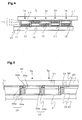
- Patent Documents 2 and 3 there has been proposed a dye-sensitized solar cell module having a structure shown in Fig. 11 .
- a porous semiconductor layer 112 and a catalyst layer 114 are alternately formed on two glass substrates 100 and 117 having transparent electrodes 111 and 118 formed in a comb-like shape by patterning, respectively.
- an insulating adhesive is applied between the porous semiconductor layer 112 on one substrate and the catalyst layer 114 of the other substrate.
- a dye-sensitized solar cell module (the so-called W-type module), in which a plurality of photoelectric conversion devices are connected in series, has been prepared.
- a dye-sensitized solar cell module (the so-called Z-type module) in which a plurality of photoelectric conversion devices are connected in series by providing electrical continuity between one conductive layer 121 and the other conductive layer 128 of adjacent photoelectric conversion devices 121a, 121a through a connecting conductive layer 129.
- the electrolyte layer 123 is isolated from the connecting conductive layer 129 by insulating layers 125, 125 between devices.
- a reference numeral 122 denotes a porous semiconductor layer
- a reference numeral 124 denotes a catalyst layer.
- Patent Document 1 Japanese Patent No. 2664194
- Patent Document 2 Domestic Re-Publication of PCT International Application W02002 / 052654 pamphlet
- Patent Document 3 Published Japanese Translation of a PCT application No. 2005-516364
- Patent Document 4 Japanese Unexamined Patent Publication No. 2001-357897
- the present invention was made in view of the above state of the art, it is an object of the present invention to provide a dye-sensitized solar cell module in which conversion efficiency and yield are improved and a method for manufacturing the same.
- a dye-sensitized solar cell module comprising a pair of opposed conductive substrates in which at least one of the substrates is transparent and a plurality of conductive layers are formed in parallel with one another on the each opposed surface of the substrates, a plurality of adjacent photoelectric conversion devices formed in a state of being electrically connected in series between the pair of conductive substrates, and insulating layers formed between the adjacent photoelectric conversion devices, wherein the photoelectric conversion devices have a porous semiconductor layer adsorbing a dye, an electrolyte layer and a catalyst layer and the insulating layer is formed by dividing into two or more times in the direction of a substrate thickness.
- a method for manufacturing a dye-sensitized solar cell module comprising the steps of: (A) providing a pair of substrates, in which at least one of the substrates is transparent and a plurality of conductive layers are formed in parallel with one another on the each surface of the substrates, and forming a plurality of strap-form insulating layers by dividing into two or more times in the direction of a substrate thickness at predetermined intervals on the conductive layers and on the surface of substrate of one substrate or both substrates of the pair of substrates, and (B) forming a photoelectric conversion device having a porous semiconductor layer adsorbing a dye, an electrolyte layer and a catalyst layer on the plurality of conductive layers, wherein the step of forming the first insulating layer in aforementioned step (A) is performed before or after the step (B).
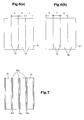
- a insulating layer of a layered structure composed of a plurality of layers between adjacent photoelectric conversion devices, and to give at least one of the insulating layers a role of controlling a gap between substrates and give other insulating layers a role of bonding and fixing at the time of bonding the substrates. Consequently, the following effects are achieved.
- a dye-sensitized solar cell module of the present invention contains a pair of opposed conductive substrates in which at least one of the substrates is transparent and a plurality of conductive layers are formed in parallel with one another on the each opposed surface of the substrates, a plurality of adjacent photoelectric conversion devices formed in a state of being electrically connected in series between the pair of conductive substrates, and insulating layers formed between the adjacent photoelectric conversion devices, wherein the photoelectric conversion devices have a porous semiconductor layer adsorbing a dye, an electrolyte layer and a catalyst layer and the insulating layer is formed by dividing into two or more times in the direction of a substrate thickness.
- the "dye-sensitized solar cell module” is referred to as just a “solar cell module” and the "porous semiconductor layer adsorbing a dye” is referred to as just a “porous semiconductor layer”.
- the "photoelectric conversion device” means a power generating layer which has a porous semiconductor layer adsorbing a dye, an electrolyte layer and a catalyst layer and substantially contributes to power generation.
- the insulating layer is formed by dividing into two or more times in the direction of a substrate thickness
- the insulating layer has a layer structure of two or more layers.
- This "layer structure”, as shown in Figs. 9 and 10 includes the form in which a second insulating layer to exert an adhesion effect is crushed due to bonding of the substrates in manufacturing a solar cell module, and crushed second insulating layer adheres to a periphery of a first insulating layer and a third insulating layer.
- Fig. 9 shows the case where the insulating layer has a two-layer structure
- Fig. 10 shows the case where the insulating layer has a three-layer structure.
- the first insulating layer of the two-layer structure and the first and the third insulating layers of the three-layer structure are an insulating layer which is formed prior to the second insulating layer in production steps, and the first insulating layer and the third insulating layer are respectively formed on separate substrates.
- first and “third” in the first insulating layer and the third insulating layer do not mean an order of forming.
- a thickness of the first insulating layer is preferably a thickness of the second insulating layer or more, and more preferably a thickness which is slightly (for example, at 50 ⁇ m or less) smaller than that of the photoelectric conversion device when the first insulating layer takes a role of substantially controlling a gap between substrates and the second insulating layer takes a role of substantially bonding a pair of the substrates to each other.
- a phrase “the first insulating layer substantially controls a gap between substrates” described above means that a distance between opposed surfaces of a pair of substrates having conductive layers is substantially determined by the film thickness of the first insulating layer.
- a phrase “the second insulating layer substantially bonds a pair of the substrates to each other” described above means that the second insulating layer ultimately bonds a pair of the substrates to each other with the first insulating layer at the time of manufacturing the solar cell module of the present invention.
- a thickness of the first insulating layer at a thickness which is slightly smaller than a thickness of the photoelectric conversion device, a thickness of the second insulating layer becomes small, a small amount of a material of the second insulating layer is sufficient for use in manufacturing this solar cell module, and spread (crush) of the material of the second insulating layer in a direction of substrate plane in bonding a pair of substrates to each other becomes small.
- an area at which the second insulating layer in a solar cell module manufactured and an adjacent photoelectric conversion device overlap is small, and therefore an effective area of a light-receiving plane of the solar cell module is increased and photoelectric conversion efficiency of the solar cell module is improved.
- a material composing the first insulating layer and a material composing the second insulating layer may be the same or may be different from each other.
- the material composing the first insulating and the material composing the second insulating layer both comprise a material containing organic polymer compounds
- the first insulating layer is made of inorganic materials
- the second insulating layer is made of materials containing organic polymer compounds.
- materials composing the insulating layer will be described in detail later.
- the insulating layer may have the three layer structure further having the third insulating layer.
- the second insulating layer to exert an adhesion effect is located between the third insulating layer and the first insulating layer, and the total thickness of a thickness of the first insulating layer and a thickness of the third insulating layer is preferably a thickness of the second insulating layer or more, and more preferably a thickness which is slightly (for example, at 50 ⁇ m or less) smaller than a thickness of the photoelectric conversion device.
- the first insulating layer and the third insulating layer are favorable for taking a role of substantially controlling a gap between substrates and for the second insulating layer to take a role of substantially bonding a pair of the substrates to each other.
- a phrase "the first insulating layer and the third insulating layer substantially controls a gap between substrates" described above means that a distance between opposed surfaces of a pair of substrates having conductive layers is substantially determined by the total film thickness of the first insulating layer and the third insulating layer.
- the second insulating layer substantially bonds a pair of the substrates to each other.
- the second insulating layer ultimately bonds a pair of the substrates to each other with the first insulating layer and the third insulating layer at the time of manufacturing the solar cell module of the present invention.
- the total thickness of a thickness of the first insulating layer and a thickness of the third insulating layer is a thickness which is slightly smaller than a thickness of the photoelectric conversion device, and thereby, a film thickness of the second insulating layer becomes small, and therefore a small amount of a material of the second insulating layer is sufficient for use in manufacturing this solar cell module, and spread of the material of the second insulating layer in a direction of substrate plane in bonding a pair of substrates to each other becomes small.
- a second insulating layer in a solar cell module manufactured does not penetrate into an adjacent photoelectric conversion device (for example, an electrolyte layer), and charge transportation between the porous semiconductor layer and the catalyst layer is not inhibited and an effective area of a light-receiving plane is increased, and photoelectric conversion efficiency of the solar cell module is improved.
- materials composing the first, the second and the third insulating layers may be the same or may be different from each other.
- these materials comprise a material containing organic polymer compounds
- the first insulating layer and the third insulating layer are made of inorganic materials and the second insulating layer is made of materials containing organic polymer compounds.
- the porous semiconductor layer and the catalyst layer respectively composing the photoelectric conversion device are laminated with the electrolyte layer therebetween, but an order of laminating the respective layers from a light-receiving plane side may be the same or may be reverse as in an adjacent cell as long as a plurality of cells are electrically connected in series. That is, when the order of laminating the respective layers from a light-receiving plane side is the porous semiconductor layer, the electrolyte layer, and the catalyst layer in an cell, the same order or a reverse order is used for an adjacent cell.
- the dye-sensitized solar cell module described above is applicable for the so-called W-type module in which the orders of laminating the respective layers (porous semiconductor layer, electrolyte layer, and catalyst layer) are reverse between adjacent cells.
- a conductive layer of one substrate contact a porous semiconductor layer in a cell and a catalyst layer in another cell adjacent to one side of the cell
- a conductive layer of the other substrate contact a catalyst layer in a cell and a porous semiconductor layer in another cell adjacent to the other side of the cell, and thereby a plurality of cells are electrically connected in series.
- the present invention is applicable to a dye-sensitized solar cell module having a structure (the so-called Z-type module) in which a pair of the insulating layers are located along one photoelectric conversion device and adjacent another photoelectric conversion device, respectively, and a connecting conductive layer electrically connected to the pair of aforementioned conductive layers is formed between the pair of aforementioned insulating layers.
- the connecting conductive layer may be one layer or two or more layers, and the connecting conductive layer of two or more layers is preferably used because physical and electric contact with the conductive layers on a pair of substrates becomes better.
- a thickness of the first connecting conductive layer is preferably a thickness of the second connecting conductive layer or more, and more preferably a thickness which is slightly (for example, at 50 ⁇ m or less) smaller than that of the photoelectric conversion device.
- the first connecting conductive layer also takes a role of substantially controlling a gap between substrates together with the first insulating layer.
- the second connecting conductive layer is prevented from spreading at the time of bonding a pair of substrates to each other and can contact the conductive layers on the pair of the substrates with reliability together with the first connecting conductive layer to reduce contact resistance.
- a substrate made of a material have a light transmitting property is used for a substrate used on the side of a light-receiving plane of a solar cell module and a light transmitting property is not particularly limited for a substrate used on the side of a non-light receiving plane.
- the transparent substrate generally, glass substrates made of soda-lime float glass, quartz glass or the like, and transparent polymer sheets made of tetraacetyl cellulose (TAC), poly(ethylene terephthalate) (PET), poly(phenylene sulfide) (PPS), polycarbonate (PC), polyallylate (PA), poly(ether imide) (PEI), a phenoxy resin or the like can be used.
- TAC tetraacetyl cellulose
- PET poly(ethylene terephthalate)
- PPS poly(phenylene sulfide)
- PC polycarbonate
- PA polyallylate
- PEI poly(ether imide)
- the transparent polymer sheets are advantageous in terms of cost and flexibility.
- the conductive layers formed thereon require to be transparent.
- the substrate used on the side of a non-light receiving plane include the above-mentioned transparent substrates and metal sheets.
- the metal sheet since the metal sheet may be subject to corrosion depending on a combination of a metal material and an electrolyte, it is preferable to coat at least the surface of the metal sheet, which comes into contact with the electrolyte layer, with a corrosion-resistant metal oxide film.
- a conductive layer made of a material have a light transmitting property is used for a conductive layer used on the side of a light-receiving plane of a solar cell module and a light transmitting property is not particularly limited for a conductive layer used on the side of a non-light receiving plane.
- a material of the transparent conductive layer include indium tin complex oxide (ITO), tin oxide (SnO 2 ), fluorine-doped tin oxide (F-doped SnO 2 , FTO), and zinc oxide (ZnO).
- the conductive layer used on the side of a non-light receiving plane include the above-mentioned transparent conductive layers and opaque materials such as metal films. When the opaque material is used, it is possible to omit the reduction in a film thickness, and when the electrolyte layer includes iodine, the conductive layer preferably has iodine resistance.
- the conductive layer can be formed on the substrate by an ordinary method such as a sputtering method, a spraying method or the like.
- a film thickness of the conductive layer is preferably about 0.02 to 5 ⁇ m.
- the conductive layer preferably has a lower film resistance and a film resistance is preferably 40 ohm/ sq or less.
- a transparent conductive substrate prepared by laminating a conductive layer made of fluorine-doped tin oxide on soda-lime float glass is particularly suitable.
- a metal lead may be added in order to reduce resistance of a transparent conductive layer.
- platinum, gold, silver, copper, aluminum, nickel, and titanium are preferable.
- a metal lead wire is formed on a substrate by a sputtering method or a vapor deposition method and thereon, a transparent conductive layer of tin oxide, ITO or the like is formed. Further, the metal lead wire may be formed by a sputtering method or a vapor deposition method after the transparent conductive layer of tin oxide, ITO or the like is formed. However, since installation of the metal lead wire leads to reduction in a quantity of incident light, a thickness of the metal lead wire is preferably 0.1 mm to several mm.
- the porous semiconductor layer may have various morphological states such as a granular state, a film-form state having a large number of fine pores, and the like at the surface and inside of the layer, and preferably the film-form state.
- a semiconductor used for the porous semiconductor layer any semiconductor can be used as long as it is generally used in photoelectric conversion materials, and examples of the semiconductor include simple compounds such as titanium oxide, zinc oxide, tin oxide, iron oxide, niobium oxide, zirconium oxide, cerium oxide, tungsten oxide, silicon oxide, aluminum oxide, nickel oxide, barium titanate, strontium titanate, cadmium sulfide, lead sulfide, zinc sulfide, indium phosphide, copper-indium sulfide (CuInS 2 ), CuAlO 2 , and SrCu 2 O 2 , or combinations thereof.
- titanium oxide, zinc oxide, tin oxide, and niobium oxide are preferable, and titanium oxide is preferable from the
- titanium oxide includes various titanium oxides in narrow definition such as anatase type titanium oxide, rutile type titanium dioxide, amorphous titanium oxide, metatitanic acid and orthotitanic acid, and titanium hydroxide and hydrated titanium oxide.
- Two types of crystals, anatase type and rutile type can become any type of anatase type and rutile type depending on their production methods or heat histories, but the anatase type is common.
- titanium oxide having a high content of anatase type is preferable and a proportion of the anatase type is preferably 80% or more.
- the anatase type has a shorter wavelength at a long wave end of photoabsorption than the rutile type and a degree of reduction in photoelectric conversion due to ultraviolet lay is small.
- one or more semiconductors of the above-mentioned semiconductors can be selected and used. These semiconductors may be a single crystal or may be a polycrystal, but the polycrystal is more preferable from the viewpoint of stability, difficulty of crystal growth, and production cost. Particularly, a fine powdered (nanometer to micrometer) polycrystalline semiconductor is preferable. Further, the same or different semiconductors having two or more particle sizes may be mixed. In this case, materials of the respective particles may be the same or may be different. The ratio between average particle diameters of the semiconductor particles having different particle sizes is preferably 10-folds or more.
- the particle with a larger particle diameter (100 to 500 nm) may be mixed for the purpose of scattering incident light and improving a light trapping ratio, and the particle with a smaller particle diameter (5 to 50 nm) may be mixed for the purpose of increasing number of adsorption points to make dye adsorption better.
- a semiconductor having high adsorption action is designated as a semiconductor with a smaller particle diameter.
- Titanium oxide which is the most preferable form of the semiconductor particle, can be prepared according to methods described in various references. Further, a method for obtaining chloride by high-temperature hydrolysis, developed by Degussa AG., may be employed.
- Examples of a method for forming the porous semiconductor layer include a method in which a suspension containing semiconductor particles is applied onto a transparent conductive film and the applied suspension is dried and/or fired.
- semiconductor particles are suspended in an appropriate solvent.
- the solvent include glyme solvents such as ethylene glycol monomethyl ether, alcohol solvents such as isopropyl alcohol, alcohol base mixed solvents such as isopropyl alcohol/toluene, and water.
- a commercially available titanium oxide paste Ti-Nanoxide, D, T/SP, D/SP, produced by Solaronix S.A may be used in place of these suspensions.
- Examples of a method for applying a suspension of semiconductor particles for forming a semiconductor layer to a substrate include publicly known methods such as a doctor blade method, a squeegee method, a spin coating method and a screen printing method. Then, the applied solution is dried and/or fired. Conditions of temperature, time, atmosphere and the like required for drying and firing can be appropriately adjusted according to kinds of the substrate and the semiconductor particles to be used, and examples of the conditions for drying and firing include a temperature within a range of about 50 to 800°C, for about 10 seconds to 12 hours, and an atmosphere of air or an atmosphere of inert gas. Drying and/or firing can be performed once at one temperature, or can be performed twice or more at varying temperatures. When the porous semiconductor layer is composed of a plurality of layers, two or more suspensions of semiconductor particles having different average particle diameters are provided, and the step of applying, drying and/or firing may be repeated twice or more.
- a thickness of each layer of the porous semiconductor layer is not particularly limited, and examples of the thickness include about 0.1 to 100 ⁇ m. Further, from another point of view, the porous semiconductor layer preferably has a large specific surface area, and examples of a preferable specific surface area include about 10 to 500 m 2 /g, and preferably 10 to 200 m 2 /g. In addition, a specific surface area shown in the present invention is a value measured by a BET adsorption method.
- the semiconductor layer may be treated, for example, with an aqueous solution of titanium tetrachloride for the purpose of improving electrical connection between semiconductor particles, improving an surface area of the porous semiconductor layer, and decreasing a defective level of semiconductor particles.
- the sensitizing dye is adsorbed on the porous semiconductor layer which serves as a photoelectrode.
- various organic dyes and metal complex dyes which have absorption in a region of visible light and/or an infrared region, are used.
- organic dyes include azo dyes, quinone dyes, quinone imine dyes, quinacridone dyes, squarylium dyes, cyanine dyes, merocyanine dyes, triphenylmethane dyes, xanthene dyes, porphyrin dyes, perylene dyes, indigo dyes, and naphthalocyanine dyes.
- the organic dyes generally have a larger absorptivity than metal complex dyes having a coordinate bond conformation in which molecules bond to a transition metal.
- the metal complex dyes can also be used in addition to the above descried organic dyes.
- the metal complex dye examples thereof such as phthalocyanine dyes and ruthenium dyes containing metals such as Cu, Ni, Fe, Co, V, Sn, Si, Ti, Ge, Cr, Zn, Ru, Mg, Al, Pb, Mn, In, Mo, Y, Zr, Nb, Sb, La, W, Pt, Ta, Ir, Pd, Os, Ga, Tb, Eu, Rb, Bi, Se, As, Sc, Ag, Cd, Hf, Re, Au, Ac, Tc, Te and Rh are preferably used.
- ruthenium metal complex dyes are more preferable.
- Ruthenium535 dye produced by Solaronix S.A. expressed by the formula (1)
- Ruthenium535-bisTBA dye compound 3, produced by Solaronix S.A.
- Ruthenium620-1H3TBA dye compound 4, produced by Solaronix S.A.
- an interlock group such as a carboxyl group, an alkoxy group, a hydroxyl group, a sulfonic acid group, an ester group, a mercapto group or a phosphonyl group in a dye molecule for adsorbing dye firmly on the porous semiconductor layer.
- the dye is fixed to a semiconductor with the interlock group interposed between the dye and the semiconductor, and has a function of providing an electrical bond to facilitate an electron transfer between a dye in an excited state and a conduction band of the semiconductor.
- the solvent of the dye solution is not particularly limited as long as it is a solvent, in which a photosensitized dye to be used is dissolved, and as the solvent of the dye solution, specifically, organic solvents such as alcohols, toluene, acetonitrile, THF, chloroform or dimethylformamide can be used.
- a purified solvent is preferably used. In order to enhance the solubility of a dye in a solvent, a temperature of the solvent may be elevated, or two or more kinds of different solvents may be mixed.
- the concentration of dye in the solvent can be adjusted in accordance with the species of a dye and a solvent to be used and conditions of a dye-adsorption step.
- the concentration of dye in the solution of a dye can be appropriately adjusted in accordance with the species of a dye and a solvent to be used, but a higher concentration is preferable for improving an adsorptive function, and for example, the concentration of 1 ⁇ 10 -5 mol/liter or more is preferable.
- a material of the catalyst layer is not particularly limited as long as it is a material, which activates an oxidation-reduction reaction of the electrolyte layer described later, and examples of the material include platinum, chloroplatinic acid, and carbons (carbon black, Ketjenblack, carbon nanotube, fullerene, etc.).
- the catalyst layer can be formed by methods such as a sputtering method, thermal cracking of chloroplatinic acid, a method in which a sol solution containing a catalyst material is applied and then at least one of drying and firing is performed, or electrodeposition.
- An oxidation-reduction electrolyte used for the electrolyte layer in the present invention is not particularly limited as long as it can be generally used in batteries or solar cells, and for example, an electrolyte solution containing an oxidation-reduction species such as I - /I 3 - type, Br 2 - /Br 3 - type, Fe 2 + /Fe 3 + type, quinine/hydroquinone type oxidation-reduction species and the like can be used.
- combinations of metal iodides such as lithium iodide (LiI), sodium iodide (NaI), potassium iodide (KI), and calcium iodide (CaI 2 ) and iodine (I 2 ), combinations of tetraalkyl ammonium salt such as tetraethylammonium iodide (TEAI), tetrapropylammonium iodide (TPAI), tetrabutylammonium iodide (TBAI), and tetrahexylammonium iodide (THAI) and iodine, and combinations of metal bromides such as lithium bromide (LiBr), sodium bromide (NaBr), potassium bromide (KBr), and calcium bromide (CaBr 2 ) and bromine are preferable, and among these combinations, the combination of LiI and I 2 is particularly preferable.
- metal iodides such as lithium
- Examples of a solvent of a liquid electrolyte layer include carbonate compounds such as propylene carbonate and the like, nitrile compounds such as acetonitrile and the like, alcohols such as ethanol and the like, water, and aprotic polar materials. Among these solvents, carbonate compounds and nitrile compounds are particularly preferable. These solvents may be used as a mixture of two or more thereof.
- nitrogen-containing aromatic compounds such as t-butylpyridine (TBP), or imidazole salts such as dimethylpropylimidazole iodide (DMPII), methylpropylimidazole iodide (MPII), ethylmethylimidazole iodide (EMII), ethylimidazole iodide (EII), and hexylmethylimidazole iodide (HMII) may be added to the liquid electrolyte layer as an additive.
- the concentration of electrolyte in the liquid electrolyte layer is preferably 0.001 to 1.5 mol/liter, and particularly preferably 0.01 to 0.7 mol/liter.
- Materials of the first and the third insulating layers preferably contains an inorganic material.
- an inorganic material particles of zirconium oxide, silicon oxide, or aluminum oxide are preferable, and these materials may be used alone or in combination, and among these, a material containing silicon oxide which hardly adsorbs a dye is particularly preferable.
- An average particle diameter of these inorganic particles is 10 to 500 ⁇ m, preferably 20 to 300 ⁇ m, and more preferably 20 to 100 ⁇ m.
- the first insulating layer and the third insulating layer can be formed by applying a suspension containing particles of, for example, the above-mentioned inorganic material onto the substrate surface and the conductive layer and drying and/or firing applied suspension.
- a suspension containing particles of, for example, the above-mentioned inorganic material onto the substrate surface and the conductive layer and drying and/or firing applied suspension.
- inorganic particles are suspended in an appropriate solvent to prepare a suspension.
- the solvent include glyme solvents such as ethylene glycol monomethyl ether, alcohol solvents such as isopropyl alcohol, alcohol base mixed solvents such as isopropyl alcohol/toluene, and water.
- a commercially available inorganic material paste may be used in place of these suspensions.
- Examples of a method for applying a suspension containing inorganic particles to a substrate include publicly known methods such as a doctor blade method, a squeegee method, a spin coating method and a screen printing method. Conditions of temperature, time, atmosphere and the like required for drying and/or firing the applied solution can be appropriately adjusted according to materials of the substrate and the semiconductor to be used. Further, the first insulating layer and the third insulating layer may be formed using the same material and the same method as those in the second insulating layer described later.
- the catalyst layer when the catalyst layer is formed by applying a sol solution of a catalyst material, and then performing at least one of drying and firing, it is preferable to form the catalyst layer after forming the insulating layer.
- a film thickness of the insulating layer is preferably 1 to 50 ⁇ m from the viewpoint of preventing flying of a catalyst material, and more preferably 5 to 30 ⁇ m.
- an insulating layer means a first insulating layer and a third insulating layer formed prior to the second insulating layer. Furthermore, in the present invention, it is preferable to form the insulating layers (the first and the third insulating layers) on the conductive substrate before forming the porous semiconductor layer, the catalyst layer and the electrolyte layer from the viewpoint of ease of a production step and improving properties of a produced solar cell module. The reason for this is that if the porous semiconductor layer is formed on the substrate before forming the insulating layers, the porous semiconductor layer becomes physical interference and it becomes difficult to form the insulating layer.
- the photosensitive resins include photosensitive polymers in which a resin itself absorbs light energy to be cured, photosensitive compound-containing polymers in which a photosensitive compound (sensitizer) in a resin absorbs light energy and thereby the resin is cured, and photopolymerizable monomer-containing polymers in which a photopolymerizable monomer in a resin absorbs light energy, and thereby, the monomer is converted to a resin and the resin is cured.
- the photosensitive resin is not particularly limited, and for example, a commercially available ultraviolet-curable resin (e.g., 31X-101: produced by Three Bond Co., Ltd.) can be used.
- the thermosetting resin is not particularly limited, and examples of the thermosetting resin include epoxy resins, acrylic resins, phenolic resins, polyester resins, and polyurethane resins; and a thermosetting resin (for example, 2212B: produced by Three Bond Co., Ltd.) having a curing temperature of 200°C or less, more preferably 150°C or less, can be used from the viewpoint of not degrading a dye.
- These resins are applied onto the first insulating layer or onto the conductive film and the substrate, and cured by irradiating ultraviolet lay to the resin or by heating the resin after a pair of substrates is bonded to each other to connect and fix two substrates to each other.
- the first connecting conductive layer As a material of the first connecting conductive layer, metals, carbon materials and conductive oxides, which have small specific resistance, are preferable, and specifically, platinum, gold, silver, copper, aluminum, nickel, titanium, graphite, carbon nanotube, fullerene, indium tin complex oxide (ITO), tin oxide (SnO 2 ), fluorine-doped tin oxide (F-doped SnO 2 , FTO), and zinc oxide (ZnO) are preferable.
- the first connecting conductive layer can be formed by applying a suspension containing particles of platinum, gold, silver, copper, aluminum, nickel or titanium onto the conductive substrate and drying and/or firing the applied suspension.
- the above-mentioned particles are suspended in an appropriate solvent to prepare a suspension:
- the solvent include glyme solvents such as ethylene glycol monomethyl ether, alcohols such as isopropyl alcohol, alcohol base mixed solvents such as isopropyl alcohol/toluene, and water.
- a commercially available conductive paste may be used in place of these suspensions.
- a method for applying a suspension onto a conductive substrate include publicly known methods such as a doctor blade method, a squeegee method, a spin coating method and a screen printing method. Then, the applied solution is dried and/or fired. Conditions of temperature, time, atmosphere and the like required for drying and/or firing can be appropriately adjusted according to materials of the substrate and the porous semiconductor layer to be used.
- the second connecting conductive layer is preferably made of metals or carbon materials which have small specific resistance, and specifically, it is preferably made of platinum, gold, silver, copper, aluminum, nickel, titanium, graphite, carbon nanotube, or fullerene.
- a conductive paste containing particles of the above-mentioned metals or carbon materials can be used as a material for forming the second connecting conductive layer.
- a conductive paste having a curing temperature of 200°C or less, more preferably 150°C or less, from the viewpoint of not degrading a dye for example, commercialized products such as a conductive paste produced by Fujikura Kasei Co., Ltd., a polymer type conductive paste produced by Asahi Chemical Research Laboratory Co., Ltd. and the like can be used.
- the dye-sensitized solar cell module of the present invention which has the above-mentioned constitution, can be manufactured by a method for manufacturing a dye-sensitized solar cell module in which a pair of substrates, in which at least one of the substrates is transparent and a plurality of conductive layers are formed in parallel with one another on the each opposed surface of the substrates, is provided, comprising the step (A) of forming a plurality of strap-form insulating layers separately divided into two or more fotmations in a direction of a substrate thickness at predetermined intervals on the conductive layers of one substrate or both substrates of the pair of substrates and on the surfaces of substrates, and the step (B) of forming a photoelectric conversion device having a porous semiconductor layer adsorbing a dye, an electrolyte layer and a catalyst layer on the plurality of conductive layers, wherein the step of forming a first insulating layer in the above-mentioned step (A) is performed before or after the step (B
- Fig. 1 is a sectional view showing a schematic constitution of a dye-sensitized solar cell module (W-type module) of Embodiment 1 of the present invention.
- a first photoelectric conversion device 1a and a second photoelectric conversion device 1b are alternately located in a state in which the first photoelectric conversion device 1a and the second photoelectric conversion device 1b are electrically connected in series between a pair of substrates 10, 17 having a plurality of conductive layers 11, 18 formed in parallel with one another on the surface of the substrates.
- a lower substrate in Fig. 1 is taken as a light-receiving plane side, and at least the lower substrate 10 and the conductive layer 11 have a light transmitting property.
- the first photoelectric conversion device 1a is formed by laminating the porous semiconductor layer 12, the electrolyte layer 13, and the catalyst layer 14 in succession from the lower substrate 10 and the second photoelectric conversion device 1b is formed by laminating the catalyst layer 14, the electrolyte layer 13, and the porous semiconductor layer 12 in succession from the lower substrate 10.
- the lower conductive layer 11 is divided into two or more parts so as to be connected to the porous semiconductor layer 12 of the first photoelectric conversion device 1a and the catalyst layer 14 of the second photoelectric conversion device 1b adjacent to one side of the first photoelectric conversion device 1a and the upper conductive layer 18 is divided into two or more parts so as to be connected to the catalyst layer 14 of the first photoelectric conversion device 1a and the porous semiconductor layer 12 of the second photoelectric conversion device 1b adjacent to the other side of the first photoelectric conversion device 1a.
- the insulating layer 16 formed by laminating the first insulating layer 16a and the second insulating layer 16b are formed between the first photoelectric conversion device 1a and the second photoelectric conversion device 1b
- the first insulating layer 16a is located on the transparent conductive layer 11 and between two adjacent transparent conductive layers 11 on the substrate 10
- the second insulating layer 16b is located between two adjacent transparent conductive layers 11 on the substrate 17 and on the transparent conductive layer 11.
- thicknesses of the conductive layers 11, 18 are 0.1 to 1 ⁇ m, respectively, a thickness of the porous semiconductor layer 12 is 1 to 50 ⁇ m, and a thickness of the catalyst layer 14 is 5 nm to 1 ⁇ m, but a catalyst material may adheres to the conductive layer in a cluster. Further, a thickness of the insulating layer 16 is 1 to 50 ⁇ m, and this thickness is equal to a distance between a lower or upper conductive layer and an upper or lower substrate, and a thickness of the first insulating layer 16a is 1 to 50 ⁇ m and a thickness of the second insulating layer 16b is less than 50 ⁇ m.
- the solar cell module shown in Fig. 1 can be produced according to the following procedure.
- a plurality of insulating layers (first insulating layer 16a) are formed on the conductive layer 11 and the surface of one substrate 10 of a pair of substrates 10, 17, and then in the step (B), the step (1) in which the porous semiconductor layer 12 and the catalyst layer 14 are formed between the insulating layers 16a on the conductive layers 11, 18 of the pair of the substrates, the step (2) in which a dye is adsorbed on the porous semiconductor layer 12, the step (3) in which an uncured resin material is applied onto the insulating layer 16a, the step (4) in which a pair of substrates 10 and 17 are overlaid on each other in such a way that the porous semiconductor layer 12 on one substrate and the catalyst layer 14 on the other substrate are opposed to each other, and the uncured resin material is cured to form a second insulating layer 16b, and
- a pair of substrates 10, 17 having a plurality of divided conductive layers 11, 18 at the surface are provided, and a plurality of insulating layers are formed on the conductive layers 11 of the substrate 10 on a light-receiving plane side and on the surface of the substrate 10 (step (A)).
- the insulating layer is a first insulating layer 16a.
- the first insulating layer 16a can be formed by the above-mentioned method.
- a reference numeral 21 represents a scribe line which divides the conductive layers 11, 18 into two or more parts.
- a thickness of the first insulating layer 16a is formed in a thickness (in this case, less than 50 ⁇ m) which is slightly smaller than a thickness (in this case, 1 to 50 ⁇ m) of cells 1a, 1b to be formed.
- the first insulating layer 16a plays a role of substantially decreasing a gap at the time of bonding the substrates and it becomes possible to reduce an amount of an uncured resin material, which is a material of the second insulating layer, applied at the time of bonding the substrates.
- a degree of spread of the uncured resin material (crush of the insulating adhesive) in a direction of substrate plane at the time of bonding becomes small, and therefore a rate of the uncured resin material to cover over a part of the porous semiconductor layer or the catalyst layer to be formed in a subsequent step can be decreased and performance of the solar cell module can be enhanced.
- a film thickness of the porous semiconductor layer is large, if a film thickness of the first insulating layer 16a is controlled, it becomes possible to bond the substrates with a small quantity of uncured resin material, and a problem that an uncured resin material (an insulating adhesive) applied to one substrate does not contact the other substrate can be solved.
- a material of the first insulating layer 16a a material having hardness after the insulating layer is formed is preferable to prevent the paste from being destroyed by a printing pressure in applying the paste of a porous semiconductor onto the conductive layer using a squeegee in a subsequent step, and if a material having hardness is used, a distance (gap) between substrates can be kept stable.
- inorganic materials for example, glass frits containing silicon oxide is preferable, as described.
- organic polymers may be used if organic polymers have hardness after ultraviolet irradiation or thermal curing.
- Step (1) As shown in Fig. 3(a) , the porous semiconductor layer 12 and the catalyst layer 14 are alternately formed between first insulating layers 16a on the conductive layer 11 of the substrate 10 on a light-receiving plane side, and as shown in Fig. 3(b) , the catalyst layer 14 and the porous semiconductor layer 12 are alternately formed between regions for forming an insulating layer on the conductive layer 18 of the substrate 17 on a non-light receiving plane side.
- the porous semiconductor layer 12 and the catalyst layer 14 can be formed by the above-mentioned method.
- a method for applying a paste of the porous semiconductor layer 12 As a method for applying a paste of the porous semiconductor layer 12, a method for applying by a dispenser and a method for applying by screen printing are preferable, and a method for applying by screen printing is most preferable.
- screen printing since the paste is pressed against a substrate at a constant pressure by a printing pressure by a squeegee even when the first insulating layer 16a exists, adhesion between the substrate and the porous insulating layer is improved compared with another methods.
- Step (2) A laminated body obtained by forming the porous semiconductor layers 12 and the catalyst layers 14 on the substrates 10, 17 is immersed in a dye solution as described above to adsorb the dye on each porous semiconductor layer 12. Then, each laminated body is withdrawn from the dye solution and dried.
- the uncured resin material of this case is a material for forming a second insulating layer 16b.
- the uncured resin material is preferably a resin having a curing temperature of 200°C or less, furthermore 150°C or less to decrease damage to a dye adsorbed on the porous semiconductor layer.
- Step (4) The respective substrates are overlaid on each other in such a way that the porous semiconductor layer 12 on the substrate 10 and the catalyst layer 14 on the substrate 17 are opposed to each other, and the uncured resin material is cured to form a second insulating layer 16b, and a pair of substrates 10, 17 are bonded to each other to be secured.
- the uncured resin material is a photosensitive material, it is cured by irradiating light (for example, ultraviolet lay) from the side of a substrate having a light transmitting property, and when the uncured resin material is a thermosetting resin, it is cured by heating at a temperature at which a dye is not degraded.
- Step (5) An electrolyte solution is filled into between a pair of substrates 10 and 17 to form an electrolyte layer 13 between the porous semiconductor layer 12 and the catalyst layer 14 of each photoelectric conversion device 1a, 1b.
- a gap part (not shown) is formed between substrates 10 and 17, and an electrolyte solution can be filled through this gap part by capillary action. Then, the gap part is sealed with a resin.
- Fig. 4 is a sectional view showing a schematic constitution of a dye-sensitized solar cell module (W-type module) of Embodiment 2 of the present invention.
- W-type module dye-sensitized solar cell module
- Fig. 4 the same reference numerals and characters are given to the constituent elements similar to Embodiment 1 shown in Fig. 1 .
- the solar cell module of Embodiment 2 has the same structure as in Embodiment 1 except that the insulating layer of this solar cell module has a structure of three layers as distinct from Embodiment 1.
- difference of a structure of this solar cell module from that of Embodiment 1 will be mainly described.
- the insulating layer 26 is formed by laminating the first insulating layer 26a, the second insulating layer 26b and the third insulating layer 26c.
- the first insulating layers 26a are formed on the conductive layer 11 and on the substrate 10 on a light-receiving plane side and the third insulating layers 26c are formed on the conductive layer 18 and on the substrate 17 on a non-light receiving plane side, and the second insulating layer 26b is formed between the first insulating layer 26a and the third insulating layer 26c.
- thicknesses of the respective layers other than the insulating layer 26 can be set at the same range of a thickness as in Embodiment 1.
- thicknesses of the first and the third insulating layers 26a, 26c are 1 to 50 ⁇ m and a thickness of the second insulating layer 26b is less than 50 ⁇ m.
- the solar cell module shown in Fig. 4 can be produced according to the following procedure.
- a plurality of insulating layers first and third insulating layers 26a, 26c
- the step (1) in which the porous semiconductor layer 12 and the catalyst layer 14 are formed between the insulating layers on the respective conductive layers 11, 18 of the pair of the substrates 10, 17, the step (2) in which a dye is adsorbed on the porous semiconductor layer 12, the step (3) in which an uncured resin material is applied onto the insulating layer, the step (4) in which a pair of substrates 10 and 17 are overlaid on each other in such a way that the porous semiconductor layer 12 on one substrate and the catalyst layer 14 on the other substrate are opposed to each other, and the uncured resin material is cured to
- a plurality of first insulating layers 26a are formed on the conductive layers 11 of one substrate 10 and on the surface of substrate 10
- a plurality of third insulating layers 26c are formed on the conductive layers 18 of the other substrate 17 and on the surface of the other substrate 17.
- the first and the third insulating layers 26a, 26c can be formed by the above-mentioned method.
- the total thickness of a thickness of the first insulating layer 26a and a thickness of the third insulating layer 26c is formed in a thickness (in this case less than 50 ⁇ m) which is slightly smaller than a thickness (in this case 1 to 50 ⁇ m) of photoelectric conversion devices 1a, 1b to be formed.
- Step (1) As with description in Fig. 3(a) , the porous semiconductor layer 12 and the catalyst layer 14 are alternately formed between first insulating layers 26a on the conductive layer 11 of the substrate 10 on a light-receiving plane side, and the catalyst layer 14 and the porous semiconductor layer 12 are alternately formed between third insulating layers 26c on the conductive layer 18 of the substrate 17 on a non-light receiving plane side.
- the porous semiconductor layer 12 and the catalyst layer 14 can be formed by the above-mentioned method.
- Step (2) A laminated body obtained by forming the porous semiconductor layers 12 and the catalyst layer 14 on the substrates 10, 17 is immersed in a dye solution as described above to adsorb the dye on each porous semiconductor layer 12. Then, each laminated body is withdrawn from the dye solution and dried.
- the uncured resin material of this case is a material for forming a second insulating layer 26b.
- the uncured resin material may be applied onto both first insulating layer 26a and third insulating layer 26c in about half the amount of resin material to be applied in applying to only one layer for each insulating layer.
- Step (4) The respective substrates are overlaid on each other in such a way that the porous semiconductor layer 12 on the substrate 10 and the catalyst layer 14 on the substrate 17 are opposed to each other, and the uncured resin material is cured to form a second insulating layer 26b, and a pair of substrates 10, 17 are bonded to each other to be secured.
- the uncured resin material is a photosensitive material, it is cured by irradiating light (for example, ultraviolet lay) from the side of a substrate having a light transmitting property, and when the uncured resin material is a thermosetting resin, it is cured by heating at a temperature at which a dye is not degraded.
- Step (5) An electrolyte solution is filled into between a pair of substrates 10 and 17 to form an electrolyte layer 13 between the porous semiconductor layer 12 and the catalyst layer 14 of each photoelectric conversion device 1a, 1b.
- a gap part (not shown) is formed between substrates 10 and 17, and an electrolyte solution can be filled through this gap part by capillary action. Then, the gap part is sealed with a resin.
- Fig. 5 is a sectional view showing a schematic constitution of a dye-sensitized solar cell module of Embodiment 3 of the present invention.
- a plurality of photoelectric conversion device 3a having the same constitutions are located in a state of being electrically connected in series between a pair of substrates 30, 37 having a plurality of conductive layers 31, 38 on the surface of the substrates.
- a lower substrate in Fig. 5 is taken as a light-receiving plane side, and at least the lower substrate 30 and the conductive layer 31 have a light transmitting property.
- the photoelectric conversion device 3a is formed by laminating the porous semiconductor layer 32, the electrolyte layer 33, and the catalyst layer 34 in succession from the lower substrate 30, and the upper and lower conductive layers 31 and 38 are divided into two or more parts so as to be connected to only the porous semiconductor layer 32 and the catalyst layer 34, respectively, in the respective photoelectric conversion devices 3a.
- Fig. 6(a) shows a plurality of conductive layers 31 formed in parallel with one another on the surface of the substrate 30, and
- Fig. 6(b) shows a plurality of conductive layers 38 formed in parallel with one another on the surface of the substrate 37
- a reference numeral 21 represents a scribe line which divides the conductive layers 31, 38 into two or more parts.
- each insulating layer 36 is composed of the first insulating layer 36a and the second insulating layer 36b as with Embodiment 1 and the connecting conductive layer 39 formed by laminating a first connecting conductive layer 39a and a second connecting conductive layer 39b.
- the first insulating layer 36a is formed on the lower conductive layer 31 in a state of contacting the porous semiconductor layer 32 and the second insulating layer 36b is formed between the upper adjacent conductive layer 38, 38 in a state of contacting the substrate 37.
- the first insulating layer 36a is formed on the lower substrate 30 between the adjacent conductive layers 31 and 31 and the second insulating layer 36b is formed in a state of contacting the upper conductive layer 38.
- first connecting conductive layer 39a is in contact with the lower conductive layer 31 and a second connecting conductive layer 39b is in contact with the upper conductive layer 38.
- constituent materials of the first connecting conductive layer 39a and the second connecting conductive layer 39b are preferably materials describe above.
- a plurality of photoelectric conversion devices 3a each of which is formed by laminating the porous semiconductor layer 32, the electrolyte layer 33, and the catalyst layer 34 in this order from the light-receiving plane side can be electrically connected through the connecting conductive layer 39.
- thicknesses of the conductive layers 31, 38 are 0.1 to 1 ⁇ m, respectively, a thickness of the porous semiconductor layer 32 is 1 to 50 ⁇ m, and a thickness of the catalyst layer 34 is 5 nm to 1 ⁇ m. Further, a thickness of the insulating layer 36 is 1 to 50 ⁇ m, and this thickness is equal to a distance between a lower or upper conductive layer and an upper or lower substrate, and a thickness of the first insulating layer 36a is 1 to 50 ⁇ m and a thickness of the second insulating layer 36b is less than 50 ⁇ m.
- a thickness of the connecting conductive layer 39 is 1 to 50 ⁇ m, and this thickness is equal to a distance between a lower conductive layer and an upper conductive layer, and a thickness of the first connecting conductive layer 39a is 1 to 50 ⁇ m and a thickness of the second connecting conductive layer 39b is less than 50 ⁇ m.
- the solar cell module shown in Fig. 5 can be produced according to the following procedure.
- the step (A) further comprises a step of forming a strap-form connecting conductive layer (first connecting conductive layer 39a) on a conductive layer 31 of one substrate 30, and in the step (A), after the formation of the connecting conductive layer, insulating layers (first insulating layers 36a) adjacent to both sides of each connecting conductive layer are formed on the conductive layer 31 and on the substrate surface before or after performing the above-mentioned step (B), and the step (B) comprises the step (1) in which the porous semiconductor layer 32 and the catalyst layer 34 are formed on the respective conductive layers 31, 38 of the pair of the substrates 30, 37, the step (2) in which a dye is adsorbed on the porous semiconductor layer 32, the step (3) in which an uncured resin material is applied onto the insulating layer, the step (4) in which a pair of substrates 30 and 37 are overlaid on each other in such a way that the porous semiconductor layer 32 on one substrate and the catalyst layer
- a plurality of strap-form connecting conductive layer are formed on the respective conductive layers 31 on the surface of one substrate 30 (refer to Fig. 6(a) ).
- This connecting conductive layer is a first connecting conductive layer 39a.
- the first connecting conductive layer 39a can be formed by the above-mentioned method.
- insulating layers adjacent to both sides of each first connecting conductive layer 39a are formed. These insulating layers are a first insulating layer 36a.
- one of a pair of first insulating layers 36a adjacent to one first connecting conductive layer 39a is formed on the conductive layer 31 and the other is formed on the substrate 30 (refer to Fig. 5 ).
- Embodiment 3 in the above-mentioned step (B), the step of applying an uncured conductive material onto the connecting conductive layer immediately before or after the above-mentioned step (3) of applying an uncured resin material onto the first insulating layer 36a, and the step of curing the uncured conductive material concurrently with or immediately after the above-mentioned step (4) of curing the uncured resin material are carried out.
- a drying step may be added after the uncured conductive material is applied.
- Step (B) will be specifically described.
- the following steps (1) to (5) are performed.
- the porous semiconductor layer 32 and the catalyst layer 34 can be formed by the above-mentioned method.
- Step (2) A laminated body obtained by forming the porous semiconductor layers 32 on the substrate 30 is immersed in a dye solution as described above to adsorb the dye on each porous semiconductor layer 32. Then, each laminated body is withdrawn from the dye solution and dried.
- the uncured conductive material is a material for forming a second connecting conductive layer and the uncured resin material is a material for forming a second insulating layer 36b.
- the uncured conductive material is preferably a material having a curing temperature of 200°C or less, furthermore 150°C or less to decrease damage to a dye adsorbed on the porous semiconductor layer.
- a dye-sensitized solar cell module shown in Fig. 4 was prepared according to the following procedure. First, two glass substrates with SnO 2 coating produced by Nippon Sheet Glass Co., Ltd having a size of 43 mm ⁇ 65 mm was provided as substrates 10, 17 on which a conductive layer made of a SnO 2 is respectively formed as shown in Figs. 2(a) and 2(b) . Next, scribing was performed by irradiating laser light (YAG laser, basic wavelength 1.06 ⁇ m, manufactured by SEISHIN TRADING Co., Ltd.) to a SnO 2 of a conductive layer in such a way that in Fig.
- laser light YAG laser, basic wavelength 1.06 ⁇ m, manufactured by SEISHIN TRADING Co., Ltd.
- a dimension I is 15.5 mm
- a dimension J is 15.5 mm
- a dimension K is 15.5 mm
- a dimension L is 15.5 mm to evaporate the SnO 2 .
- the dimensions I to L are the same, but these dimensions are not drawn to scale for convenience in Fig. 2 .
- a width of a region A is taken as 16 mm
- a width of a region B is taken as 10 mm
- a width of a region C is taken as 5 mm
- a width of a region D is taken as 7 mm
- a width of a region E is taken as 4 mm
- a width of a region F is taken as 10 mm
- a width of a region H is taken as 5 mm
- glass frits produced by Noritake Co., Ltd.
- glass frits which are a material of a first insulating layer
- a first insulating layer 26a was formed on the substrate 10 and a third insulating layer 26c was formed on the substrate 17.
- the first insulating layer 26a and the third insulating layer 26b respectively have a film thickness of about 25 ⁇ m and a width of about 500 ⁇ m. Measurement of the film thickness was performed with SURFCOM 1400A (manufactured by TOKYO SEIMITSU Co., Ltd.).
- a platinum film was formed in a film thickness of about 5 nm at a deposition rate of 0.1 ⁇ /sec as a catalyst layer 14 in the respective regions C of the substrates 10 and 17 using an electron beam vapor deposition machine EVD-500A (manufactured by ANELVA Corp.).
- a commercially available titanium oxide paste (produced by Solaronix S.A., trade name: Ti-Nanoxide D/SP, average particle diameter: 13 nm) was applied to the regions A, D and B of the substrate 10 and the regions D and D of the substrate 17 using a screen plate with an opening of 5.25 mm ⁇ 50 mm and a screen-printing machine (LS-150 manufactured by NEWLONG SEIMITSU KOGYO Co., Ltd.), and the applied titanium oxide paste was leveled at room temperature for 1 hour, and the resulting coat was pre-dried at 80°C for 20 minutes and fired at 450°C for 1 hour.
- LS-150 manufactured by NEWLONG SEIMITSU KOGYO Co., Ltd.
- This process step was repeated five times and thereby a titanium oxide film having a film thickness of 30 ⁇ m was obtained as a porous semiconductor layer 12. Measurement of the film thickness was performed with SURFCOM 1400A (manufactured by TOKYO SEIMITSU Co., Ltd.).
- a dye was adsorbed on each porous semiconductor layer 12 according to the following procedure.
- a sensitizing dye Ruthenium620-1H3TBA dye (produced by Solaronix S.A.) was used, and a mixed solution (concentration of the sensitizing dye; 4 ⁇ 10 -4 mol/liter) of this dye in a mixed solvent of acetonitrile (produced by Aldrich Chemical Company) and t-butyl alcohol (produced by Aldrich Chemical Company) in proportions by volume of 1:1 was prepared.
- a laminated body having the porous semiconductor layers 12 on the substrates 10, 17 was immersed in this mixed solution and left standing at a temperature of 40°C for 20 hours. Then, the laminated body was cleaned with ethanol (produced by Aldrich Chemical Company) and dried.
- a solution which was prepared by dissolving DMPII (produced by SHIKOKU CHEMICALS Corp.) with a concentration of 0.6 mol/l, LiI (produced by Aldrich Chemical Company) with a concentration of 0.1 mol/l, TBP (produced by Aldrich Chemical Company) with a concentration of 0.5 mol/l, and I 2 (produced by TOKYO CHEMICAL INDUSTRY Co., Ltd.) with a concentration of 0.01 mol/l in acetonitrile as an solvent, was provided.
- DMPII produced by SHIKOKU CHEMICALS Corp.
- LiI produced by Aldrich Chemical Company
- TBP produced by Aldrich Chemical Company
- I 2 produced by TOKYO CHEMICAL INDUSTRY Co., Ltd.
- an uncured UV-curable resin 31X-101 (produced by Three Bond Co., Ltd.) was applied onto the respective first insulating layer 26a of the substrate 10 using a dispenser (manufactured by EFD Corporation). In this time, an application speed and a discharge pressure were adjusted in such a way that a film thickness of an applied film is about 45 ⁇ m.
- a solar cell module corresponding to Fig. 4 was prepared by filling an oxidation-reduction electrolyte solution through a gap between the above two substrates by capillary action, and the filling portion was sealed with a photosensitive resin or a thermosetting resin.
- photoelectric conversion efficiency was taken as a value determined by multiplying Voc and FF by a value obtained by dividing Isc by an area of an aperture area (area surrounding several exterior frames of a photoelectric conversion device in a module).
- the solar cell module was decomposed, and the first, the second and the third insulating layers 26a, 26b and 26c were observed with an optical microscope SZX-12 (manufactured by Olympus Corp.), and consequently it was found that the second insulating layer 26b was crushed as shown in Fig. 10 and a film thickness of the second insulating layer 26b was 2 ⁇ m (at crushed portion).
- a solar cell module corresponding to Fig. 1 was prepared in the same manner as in Example 1 except that the first insulating layer 16a was formed on only the substrate 10 and a film thickness of the porous semiconductor layer 12 was 15 ⁇ m and a film thickness of the first insulating layer 16a was about 30 ⁇ m in Example 1.
- Photoelectric conversion efficiency was measured by irradiating light with an intensity of 1 kW/m 2 (an AM 1.5 Solar Simulator) to the resulting solar cell module, and the result of measurement is shown in Table 1.
- the solar cell module was decomposed, and the first insulating layer 16a and the second insulating layer 16b were observed with an optical microscope SZX-12 (manufactured by Olympus Corp.), and consequently it was found that the second insulating layer 16b was crushed as shown in Fig. 9 and a film thickness of the second insulating layer 26b was 1 ⁇ m (at crushed portion).
- Example 3 a solar cell module was prepared in the same manner as in Example 1 except for applying a catalyst paste (trade name: Pt-Catalyst T/SP, produced by Solaronix S.A.), which is a material of a catalyst layer, using a screen-printing machine (LS-150, manufactured by NEWLONG SEIMITSU KOGYO Co., Ltd.), and firing the applied catalyst paste at 450°C for 1 hour to form a catalyst layer.
- a photoelectric conversion efficiency was measured by irradiating light with an intensity of 1 kW/m 2 (an AM 1.5 Solar Simulator) to the resulting solar cell module, and the result of measurement is shown in Table 1.
- Example 4 a solar cell module was prepared in the same manner as in Example 1 except for adjusting a pressure of a screen-printing machine in such a way that film thicknesses of a first and a third insulating layers 26a and 26c were about 12 ⁇ m.
- a photoelectric conversion efficiency was measured by irradiating light with an intensity of 1 kW/m 2 (an AM 1.5 Solar Simulator) to the resulting solar cell module, and the result of measurement is shown in Table 1.
- the solar cell module was decomposed and film thicknesses of the first, the second and the third insulating layers were observed with an optical microscope SZX-12 (manufactured by Olympus Corp.), and consequently it was found that the film thicknesses were 11 ⁇ m, 6 ⁇ m and 12 ⁇ m, respectively.
- Example 5 a solar cell module was prepared in the same manner as in Example 1 except for adjusting a mesh count of a screen plate in such a way that film thicknesses of a first and a third insulating layers 26a and 26c were about 8 ⁇ m.
- a photoelectric conversion efficiency was measured by irradiating light with an intensity of 1 kW/m 2 (an AM 1.5 Solar Simulator) to the resulting solar cell module, and the result of measurement is shown in Table 1.
- the solar cell module was decomposed and film thicknesses of the first, the second and the third insulating layers were observed with an optical microscope SZX-12 (manufactured by Olympus Corp.), and consequently it was found that the film thicknesses were 8 ⁇ m, 14 ⁇ m and 9 ⁇ m, respectively.
- Example 6 a solar cell module was prepared in the same manner as in Example 1 except for adjusting a mesh count of a screen plate in such a way that film thicknesses of a first and a third insulating layers 26a and 26c were about 30 ⁇ m.
- a photoelectric conversion efficiency was measured by irradiating light with an intensity of 1 kW/m 2 (an AM 1.5 Solar Simulator) to the resulting solar cell module, and the result of measurement is shown in Table 1.
- the solar cell module was decomposed and film thicknesses of the first, the second and the third insulating layers were observed with an optical microscope SZX-12 (manufactured by Olympus Corp.), and consequently it was found that the film thicknesses were 28 ⁇ m, 1 ⁇ m and 27 ⁇ m, respectively.
- a solar cell module of Comparative Example 1 was prepared in the same manner as in Example 1 except that after the catalyst layer 14 and the porous semiconductor layer 12 were formed, the first and the third insulating layers were formed and a film thickness of the porous semiconductor layer 12 was 15 ⁇ m in Example 1.
- a photoelectric conversion efficiency was measured by irradiating light with an intensity of 1 kW/m 2 (an AM 1.5 Solar Simulator) to the resulting solar cell module, and the result of measurement is shown in Table 1.
- a solar cell module of Comparative Example 2 was prepared in the same manner as in Example 1 except that in Example 1, the first insulating layer 26a and the third insulating layer 26c were formed, but in Comparative Example 2, an uncured resin was applied in an applied film thickness of 40 ⁇ m on the substrate without forming the first insulating layer and the third insulating layer and then the applied uncured resin was cured to form the second insulating layer.
- the porous semiconductor layer titanium oxide film
- Comparative Example 3 a solar cell module of Comparative Example 3 was prepared in the same manner as in Comparative Example 2 except for adjusting an application speed and a discharge pressure in such a way that an applied film thickness is 140 ⁇ m using a dispenser (manufactured by EFD Corp.). In this case, an uncured resin at and about a substrate center was penetrated into between the porous semiconductor layer and the catalyst layer when two substrates were bonded to each other. A photoelectric conversion efficiency was measured by irradiating light with an intensity of 1 kW/m 2 (an AM 1.5 Solar Simulator) to the resulting solar cell module, and the result of measurement is shown in Table 1.
- a solar cell module was prepared in the same manner as in Comparative Example 1 except for forming a catalyst paste (trade name: Pt-Catalyst T/SP, produced by Solaronix S.A.), which is a material of a catalyst layer, using a screen-printing machine (LS-150 manufactured by NEWLONG SEIMITSU KOGYO Co., Ltd.), and firing the applied catalyst paste at 450°C for 1 hour to form a catalyst layer.
- a photoelectric conversion efficiency was measured by irradiating light with an intensity of 1 kW/m 2 (an AM 1.5 Solar Simulator) to the resulting solar cell module, and the result of measurement is shown in Table 1.
- a solar cell module was prepared in the same manner as in Comparative Example 2 except for forming a catalyst paste (trade name: Pt-Catalyst T/SP, produced by Solaronix S.A.), which is a material of a catalyst layer, using a screen-printing machine (LS-150 manufactured by NEWLONG SEIMITSU KOGYO Co., Ltd.), and firing the applied catalyst paste at 450°C for 1 hour to form a catalyst layer.
- a photoelectric conversion efficiency was measured by irradiating light with an intensity of 1 kW/m 2 (an AM 1.5 Solar Simulator) to the resulting solar cell module, and the result of measurement is shown in Table 1.
- a solar cell module shown in Fig. 5 was formed according to the following procedure.
- a SnO 2 layer was formed in a comb-like shape by patterning setting a pitch (a width of the region B), at which a unit photoelectric conversion device is formed, at 8 mm by irradiating laser light (YAG laser) to the SnO 2 layer in such a way that a width of the region A is 18 mm, a width of the region B is 8 mm and a width of the region G is 10 mm to evaporate the SnO 2 .
- a silver paste (produced by Noritake Co., Ltd.), which is a material for forming a first connecting conductive layer 39a, was applied along a scribe line 21 on right three conductive layers 31 on the substrate 30 shown in Fig. 6(a) , and the applied paste was pre-dried at 80°C for 20 minutes and then fired at 450°C for 1 hour to form a first connecting conductive layer 39a having a film thickness of 22 ⁇ m and a width of 300 ⁇ m (refer to Fig. 5 and Fig. 7 ).
- glass frits produced by Noritake Co., Ltd.
- LS-150 manufactured by NEWLONG SEIMITSU KOGYO Co., Ltd.
- the applied glass frits were pre-dried at 100°C for 10 minutes and then fired at 450°C for 1 hour to form a first insulating layer 36a, 36a having a film thickness of 21 ⁇ m and a width of 500 ⁇ m (refer to Fig. 5 and Fig. 7 ).
- a porous semiconductor layer 32 was formed by the same method as in Example 1, as shown in Fig. 8(a) , on a conductive layer 31 of the substrate 30 between the first connecting conductive layers 39a.
- a dye was adsorbed on each semiconductor layer 32 according to the following procedure.
- a sensitizing dye Ruthenium620-1H3TBA dye (produced by Solaronix S.A.) was used, and a mixed solution (concentration of the sensitizing dye; 4 ⁇ 10 -4 mol/liter) of this dye in a mixed solvent of acetonitrile and t-butyl alcohol in proportions by volume of 1:1 was prepared.
- a laminated body having the porous semiconductor layers 32 formed on the substrate 30 was immersed in this mixed solution and left standing at a temperature of 40°C for 20 hours. Thereby, the sensitizing dye was adsorbed on the inside of the porous semiconductor layers 32 in an amount about 7 ⁇ 10 -8 mol/cm 2 . Then, the laminated body was cleaned with ethanol (produced by Aldrich Chemical Company) and dried.
- a platinum film was formed in a film thickness of about 5 nm on the conductive layer 38 of the substrate 37 shown in Fig. 8(b) at a deposition rate of 0.1 ⁇ /sec as a catalyst layer using an electron beam vapor deposition machine EVD-500A (manufactured by ANELVA Corp.).
- a solution which was prepared by dissolving DMPII with a concentration of 0.6 mol/l, LiI with a concentration of 0.1 mol/l, TBP with a concentration of 0.5 mol/l, and I 2 with a concentration of 0.01 mol/l in acetonitrile as a solvent, was provided.
- an uncured UV-curable resin 31X-101 (produced by Three Bond Co., Ltd.) was applied onto the first insulating layer 36a, and furthermore, a conductive silver paste (produced by Fujikura Kasei Co., Ltd., trade name: "DOTITE") was applied onto the first connecting conductive layers 39a, and two substrates 30, 37 were bonded to each other with the porous semiconductor layer 32 of one substrate and the catalyst layer 34 of the other substrate opposed to each other.
- DOTITE Fujikura Kasei Co., Ltd., trade name: "DOTITE”
- a solar cell module corresponding to Fig. 5 was prepared by filling the electrolyte solution through a gap between two substrates 30 and 37 by capillary action, and applying an UV-curable material 31X-101 (produced by ThreeBond Co., Ltd.) to the periphery of the gap, and irradiating ultraviolet lay to the applied ultraviolet curable material.
- a photoelectric conversion efficiency was measured by irradiating light with an intensity of 1 kW/m 2 (an AM 1.5 Solar Simulator) to the resulting solar cell module, and the result of measurement is shown in Table 1.
- a solar cell module of Comparative Example 6 was prepared in the same manner as in Example 7 except that the first insulating layer 36a in Example 7 was formed after the porous semiconductor layer 32 was formed, and the second insulating layer and the second connecting conductive layer in Example 7 were omitted.
- a photoelectric conversion efficiency was measured by irradiating light with an intensity of 1 kW/m 2 (an AM 1.5 Solar Simulator) to the resulting solar cell module, and the result of measurement is shown in Table 1.
Landscapes
- Engineering & Computer Science (AREA)
- Power Engineering (AREA)
- Chemical & Material Sciences (AREA)
- Chemical Kinetics & Catalysis (AREA)
- Electrochemistry (AREA)
- Microelectronics & Electronic Packaging (AREA)
- Hybrid Cells (AREA)
- Photovoltaic Devices (AREA)
- Connection Of Batteries Or Terminals (AREA)
Applications Claiming Priority (2)
| Application Number | Priority Date | Filing Date | Title |
|---|---|---|---|
| JP2006187010 | 2006-07-06 | ||
| PCT/JP2007/063318 WO2008004556A1 (fr) | 2006-07-06 | 2007-07-03 | Module de cellule solaire sensible aux colorants et procédé de fabrication correspondant |
Publications (3)
| Publication Number | Publication Date |
|---|---|
| EP2043191A1 true EP2043191A1 (fr) | 2009-04-01 |
| EP2043191A4 EP2043191A4 (fr) | 2012-09-19 |
| EP2043191B1 EP2043191B1 (fr) | 2014-05-14 |
Family
ID=38894525
Family Applications (1)
| Application Number | Title | Priority Date | Filing Date |
|---|---|---|---|
| EP07768092.4A Not-in-force EP2043191B1 (fr) | 2006-07-06 | 2007-07-03 | Module de cellule solaire sensible aux colorants et procédé de fabrication correspondant |
Country Status (6)
| Country | Link |
|---|---|
| US (1) | US8314329B2 (fr) |
| EP (1) | EP2043191B1 (fr) |
| JP (1) | JP5140588B2 (fr) |
| CN (1) | CN101512828B (fr) |
| ES (1) | ES2475730T3 (fr) |
| WO (1) | WO2008004556A1 (fr) |
Cited By (7)
| Publication number | Priority date | Publication date | Assignee | Title |
|---|---|---|---|---|
| EP2293359A1 (fr) * | 2009-09-03 | 2011-03-09 | Samsung SDI Co., Ltd. | Produit d'obturation, cellule solaire sensibilisée aux colorants l'incluant et procédé de fabrication de la cellule solaire sensibilisée aux colorants |
| US20120006377A1 (en) * | 2010-07-12 | 2012-01-12 | Samsung Sdi Co., Ltd. | Photoelectric conversion module |
| WO2011070401A3 (fr) * | 2009-12-10 | 2012-01-12 | Universidade De Aveiro | Modules photovoltaïques et procédé associé de fabrication - interconnexion de cellules solaires à colorant |
| EP2337041A3 (fr) * | 2009-12-18 | 2012-10-31 | LG Display Co., Ltd. | Module de cellules solaires sensibilisées aux colorants et son procédé de fabrication |
| EP2555315A1 (fr) * | 2010-04-02 | 2013-02-06 | Fujikura Co., Ltd. | Dispositif électronique et procédé pour sa fabrication |
| US8754326B2 (en) | 2008-10-30 | 2014-06-17 | Fujikura Ltd. | Photoelectric conversion device |
| US9607772B2 (en) | 2009-04-30 | 2017-03-28 | Sharp Kabushiki Kaisha | Porous electrode, dye-sensitized solar cell, and dye-sensitized solar cell module |
Families Citing this family (21)
| Publication number | Priority date | Publication date | Assignee | Title |
|---|---|---|---|---|
| GB0808338D0 (en) * | 2008-05-08 | 2008-06-18 | Pilkington Group Ltd | Production of coated glass |
| KR101432022B1 (ko) * | 2008-07-11 | 2014-09-23 | 주식회사 동진쎄미켐 | 염료감응 태양전지 서브모듈 |
| JP4761327B2 (ja) * | 2010-01-12 | 2011-08-31 | シャープ株式会社 | 湿式太陽電池および湿式太陽電池モジュール |
| US8669468B2 (en) * | 2010-01-19 | 2014-03-11 | Samsung Sdi Co., Ltd. | Photoelectric conversion module |
| KR101117704B1 (ko) * | 2010-06-24 | 2012-02-29 | 삼성에스디아이 주식회사 | 광전 변환 모듈과, 이의 제조 방법 |
| JP2012014849A (ja) * | 2010-06-29 | 2012-01-19 | Sony Corp | 光電変換素子およびその製造方法ならびに光電変換素子モジュールおよびその製造方法 |
| IT1402150B1 (it) * | 2010-10-04 | 2013-08-28 | Dyepower | Elementi di connessione elettrica verticale di celle fotoelettrochimiche. |
| CN102468054A (zh) * | 2010-11-15 | 2012-05-23 | 海洋王照明科技股份有限公司 | 大面积染料敏化太阳能电池及其制备方法 |
| FR2969312B1 (fr) * | 2010-12-20 | 2013-01-18 | Rhodia Acetow Gmbh | Module photovoltaique |
| IT1403764B1 (it) * | 2011-01-31 | 2013-10-31 | Dyepower | Elementi di connessione elettrica verticale di celle fotoelettrochimiche. |
| JP2012190740A (ja) * | 2011-03-14 | 2012-10-04 | Toshiba Corp | 太陽電池及びその製造方法 |
| JP5746343B2 (ja) * | 2011-06-30 | 2015-07-08 | 株式会社フジクラ | 色素増感太陽電池及びその製造方法 |
| KR101258185B1 (ko) * | 2011-07-22 | 2013-04-25 | 광주과학기술원 | 태양전지 모듈 및 이의 제조방법 |
| US9934913B2 (en) * | 2011-10-26 | 2018-04-03 | Nokia Technologies Oy | Apparatus and associated methods |
| JP2013131482A (ja) * | 2011-11-21 | 2013-07-04 | Rohm Co Ltd | 色素増感太陽電池およびその製造方法 |
| SG11201408810TA (en) | 2012-07-05 | 2015-01-29 | Taiwan Liposome Co Ltd | Methods of treating arthritis |
| US20150020863A1 (en) * | 2013-07-22 | 2015-01-22 | International Business Machines Corporation | Segmented thin film solar cells |
| WO2015174219A1 (fr) * | 2014-05-12 | 2015-11-19 | 株式会社村田製作所 | Module de production d'énergie solaire et procédé de fabrication de module de production d'énergie solaire |
| CN105185913A (zh) * | 2015-08-27 | 2015-12-23 | 常州天合光能有限公司 | 一种大面积钙钛矿太阳电池组件及其制备方法 |
| CN106090804A (zh) * | 2016-07-27 | 2016-11-09 | 杨炳 | 一种具备自发电功能的户外照明装置 |
| CN112789745A (zh) * | 2018-08-20 | 2021-05-11 | 爱普施恩有限公司 | 层压模块 |
Citations (2)
| Publication number | Priority date | Publication date | Assignee | Title |
|---|---|---|---|---|
| WO1996029716A1 (fr) * | 1995-03-23 | 1996-09-26 | Ecole Polytechnique Federale De Lausanne (Epfl) | Procede d'application d'un certain volume de sensibilisateur sur une surface |
| JP2006134870A (ja) * | 2004-10-08 | 2006-05-25 | Sharp Corp | 色素増感太陽電池およびその製造方法ならびに色素増感太陽電池モジュール |
Family Cites Families (14)
| Publication number | Priority date | Publication date | Assignee | Title |
|---|---|---|---|---|
| CH674596A5 (fr) | 1988-02-12 | 1990-06-15 | Sulzer Ag | |
| DE69513203T2 (de) | 1995-10-31 | 2000-07-20 | Ecole Polytechnique Federale De Lausanne (Epfl), Lausanne | Batterie-anordnung von fotovoltaischen zellen und herstellungsverfahren |
| AUPP931799A0 (en) | 1999-03-18 | 1999-04-15 | Sustainable Technologies Australia Limited | Methods to implement interconnects in multi-cell regenerative photovoltaic photoelectrochemical devices |
| WO2001003232A1 (fr) * | 1999-06-30 | 2001-01-11 | Catalysts & Chemicals Industries Co., Ltd. | Cellule photoelectrique |
| US6706963B2 (en) * | 2002-01-25 | 2004-03-16 | Konarka Technologies, Inc. | Photovoltaic cell interconnection |
| JP2001357897A (ja) | 2000-06-14 | 2001-12-26 | Fuji Xerox Co Ltd | 光電変換モジュール |
| JP2004319383A (ja) | 2003-04-18 | 2004-11-11 | Sharp Corp | 色素増感太陽電池モジュール |
| JP2005093252A (ja) | 2003-09-18 | 2005-04-07 | Hitachi Maxell Ltd | 光電変換素子モジュール |
| JP4411955B2 (ja) | 2003-12-10 | 2010-02-10 | パナソニック電工株式会社 | 光電変換素子モジュール |
| JP5086520B2 (ja) | 2004-07-15 | 2012-11-28 | パナソニック株式会社 | 光電変換素子モジュール |
| JP2006100025A (ja) * | 2004-09-28 | 2006-04-13 | Sharp Corp | 太陽電池モジュール |
| JP4627427B2 (ja) | 2004-10-04 | 2011-02-09 | シャープ株式会社 | 色素増感太陽電池および色素増感太陽電池モジュール |
| JP4892186B2 (ja) * | 2004-12-06 | 2012-03-07 | シャープ株式会社 | 色素増感太陽電池および色素増感太陽電池モジュール |
| JP4396574B2 (ja) | 2005-05-11 | 2010-01-13 | アイシン精機株式会社 | 色素増感型太陽電池及びその製造方法 |
-
2007
- 2007-07-03 EP EP07768092.4A patent/EP2043191B1/fr not_active Not-in-force
- 2007-07-03 CN CN2007800331746A patent/CN101512828B/zh not_active Expired - Fee Related
- 2007-07-03 JP JP2008523692A patent/JP5140588B2/ja not_active Expired - Fee Related
- 2007-07-03 US US12/307,643 patent/US8314329B2/en active Active
- 2007-07-03 ES ES07768092.4T patent/ES2475730T3/es active Active
- 2007-07-03 WO PCT/JP2007/063318 patent/WO2008004556A1/fr active Application Filing
Patent Citations (2)
| Publication number | Priority date | Publication date | Assignee | Title |
|---|---|---|---|---|
| WO1996029716A1 (fr) * | 1995-03-23 | 1996-09-26 | Ecole Polytechnique Federale De Lausanne (Epfl) | Procede d'application d'un certain volume de sensibilisateur sur une surface |
| JP2006134870A (ja) * | 2004-10-08 | 2006-05-25 | Sharp Corp | 色素増感太陽電池およびその製造方法ならびに色素増感太陽電池モジュール |
Non-Patent Citations (1)
| Title |
|---|
| See also references of WO2008004556A1 * |
Cited By (10)
| Publication number | Priority date | Publication date | Assignee | Title |
|---|---|---|---|---|
| US8754326B2 (en) | 2008-10-30 | 2014-06-17 | Fujikura Ltd. | Photoelectric conversion device |
| US9607772B2 (en) | 2009-04-30 | 2017-03-28 | Sharp Kabushiki Kaisha | Porous electrode, dye-sensitized solar cell, and dye-sensitized solar cell module |
| EP2293359A1 (fr) * | 2009-09-03 | 2011-03-09 | Samsung SDI Co., Ltd. | Produit d'obturation, cellule solaire sensibilisée aux colorants l'incluant et procédé de fabrication de la cellule solaire sensibilisée aux colorants |
| WO2011070401A3 (fr) * | 2009-12-10 | 2012-01-12 | Universidade De Aveiro | Modules photovoltaïques et procédé associé de fabrication - interconnexion de cellules solaires à colorant |
| EP2337041A3 (fr) * | 2009-12-18 | 2012-10-31 | LG Display Co., Ltd. | Module de cellules solaires sensibilisées aux colorants et son procédé de fabrication |
| US8952248B2 (en) | 2009-12-18 | 2015-02-10 | Lg Display Co., Ltd. | Dye-sensitized solar cell module and method of fabricating the same |
| EP2555315A1 (fr) * | 2010-04-02 | 2013-02-06 | Fujikura Co., Ltd. | Dispositif électronique et procédé pour sa fabrication |
| EP2555315A4 (fr) * | 2010-04-02 | 2014-12-31 | Fujikura Co Ltd | Dispositif électronique et procédé pour sa fabrication |
| US10020120B2 (en) | 2010-04-02 | 2018-07-10 | Fujikura Ltd. | Electronic device and manufacturing method for same |
| US20120006377A1 (en) * | 2010-07-12 | 2012-01-12 | Samsung Sdi Co., Ltd. | Photoelectric conversion module |
Also Published As
| Publication number | Publication date |
|---|---|
| JP5140588B2 (ja) | 2013-02-06 |
| ES2475730T3 (es) | 2014-07-11 |
| US8314329B2 (en) | 2012-11-20 |
| CN101512828B (zh) | 2011-05-11 |
| EP2043191B1 (fr) | 2014-05-14 |
| EP2043191A4 (fr) | 2012-09-19 |
| CN101512828A (zh) | 2009-08-19 |
| US20100024875A1 (en) | 2010-02-04 |
| WO2008004556A1 (fr) | 2008-01-10 |
| JPWO2008004556A1 (ja) | 2009-12-03 |
Similar Documents
| Publication | Publication Date | Title |
|---|---|---|
| EP2043191B1 (fr) | Module de cellule solaire sensible aux colorants et procédé de fabrication correspondant | |
| US10366842B2 (en) | Dye-sensitized solar cell and method for manufacturing thereof | |
| EP2421084B1 (fr) | Cellule solaire à colorant et module de cellule solaire à colorant | |
| JP5377327B2 (ja) | 光増感太陽電池モジュールおよびその製造方法 | |
| US8933328B2 (en) | Dye-sensitized solar cell module and method of producing the same | |
| JP4683396B2 (ja) | 多孔質電極、色素増感太陽電池、および色素増感太陽電池モジュール | |
| JP3717506B2 (ja) | 色素増感型太陽電池モジュール | |
| EP2131441B1 (fr) | Module de cellules solaires à colorant photosensible et son procédé de fabrication | |
| JP4448478B2 (ja) | 色素増感型太陽電池モジュール | |
| US20140096813A1 (en) | Photoelectric conversion element and photoelectric conversion element module | |
| JP5657780B2 (ja) | 光電変換素子および光電変換モジュール | |
| JP2009043482A (ja) | 色素増感太陽電池および色素増感太陽電池モジュール | |
| WO2012086377A1 (fr) | Cellule solaire à colorant et module de cellules solaires à colorant, ainsi que procédés pour leur production | |
| JP5758400B2 (ja) | 色素増感太陽電池モジュールおよびその製造方法 | |
| WO2015133030A1 (fr) | Module de conversion photoélectrique et dispositif électronique le mettant en oeuvre |
Legal Events
| Date | Code | Title | Description |
|---|---|---|---|
| PUAI | Public reference made under article 153(3) epc to a published international application that has entered the european phase |
Free format text: ORIGINAL CODE: 0009012 |
|
| 17P | Request for examination filed |
Effective date: 20090121 |
|
| AK | Designated contracting states |
Kind code of ref document: A1 Designated state(s): AT BE BG CH CY CZ DE DK EE ES FI FR GB GR HU IE IS IT LI LT LU LV MC MT NL PL PT RO SE SI SK TR |
|
| AX | Request for extension of the european patent |
Extension state: AL BA HR MK RS |
|
| DAX | Request for extension of the european patent (deleted) | ||
| A4 | Supplementary search report drawn up and despatched |
Effective date: 20120817 |
|
| RIC1 | Information provided on ipc code assigned before grant |
Ipc: H01M 2/22 20060101ALI20120810BHEP Ipc: H01L 31/04 20060101ALI20120810BHEP Ipc: H01G 9/20 20060101ALI20120810BHEP Ipc: H01M 14/00 20060101AFI20120810BHEP |
|
| 17Q | First examination report despatched |
Effective date: 20130404 |
|
| GRAP | Despatch of communication of intention to grant a patent |
Free format text: ORIGINAL CODE: EPIDOSNIGR1 |
|
| INTG | Intention to grant announced |
Effective date: 20131210 |
|
| GRAS | Grant fee paid |
Free format text: ORIGINAL CODE: EPIDOSNIGR3 |
|
| GRAA | (expected) grant |
Free format text: ORIGINAL CODE: 0009210 |
|
| RIN1 | Information on inventor provided before grant (corrected) |
Inventor name: FUKUI, ATSUSHI Inventor name: YAMANAKA, RYOHSUKE Inventor name: FUKE, NOBUHIRO |
|
| AK | Designated contracting states |
Kind code of ref document: B1 Designated state(s): AT BE BG CH CY CZ DE DK EE ES FI FR GB GR HU IE IS IT LI LT LU LV MC MT NL PL PT RO SE SI SK TR |
|
| REG | Reference to a national code |
Ref country code: GB Ref legal event code: FG4D |
|
| REG | Reference to a national code |
Ref country code: AT Ref legal event code: REF Ref document number: 668887 Country of ref document: AT Kind code of ref document: T Effective date: 20140615 |
|
| REG | Reference to a national code |
Ref country code: IE Ref legal event code: FG4D |
|
| REG | Reference to a national code |
Ref country code: DE Ref legal event code: R096 Ref document number: 602007036732 Country of ref document: DE Effective date: 20140626 |
|
| REG | Reference to a national code |
Ref country code: ES Ref legal event code: FG2A Ref document number: 2475730 Country of ref document: ES Kind code of ref document: T3 Effective date: 20140711 |
|
| REG | Reference to a national code |
Ref country code: NL Ref legal event code: VDEP Effective date: 20140514 Ref country code: AT Ref legal event code: MK05 Ref document number: 668887 Country of ref document: AT Kind code of ref document: T Effective date: 20140514 |
|
| REG | Reference to a national code |
Ref country code: LT Ref legal event code: MG4D |
|
| PG25 | Lapsed in a contracting state [announced via postgrant information from national office to epo] |
Ref country code: IS Free format text: LAPSE BECAUSE OF FAILURE TO SUBMIT A TRANSLATION OF THE DESCRIPTION OR TO PAY THE FEE WITHIN THE PRESCRIBED TIME-LIMIT Effective date: 20140914 Ref country code: LT Free format text: LAPSE BECAUSE OF FAILURE TO SUBMIT A TRANSLATION OF THE DESCRIPTION OR TO PAY THE FEE WITHIN THE PRESCRIBED TIME-LIMIT Effective date: 20140514 Ref country code: FI Free format text: LAPSE BECAUSE OF FAILURE TO SUBMIT A TRANSLATION OF THE DESCRIPTION OR TO PAY THE FEE WITHIN THE PRESCRIBED TIME-LIMIT Effective date: 20140514 Ref country code: CY Free format text: LAPSE BECAUSE OF FAILURE TO SUBMIT A TRANSLATION OF THE DESCRIPTION OR TO PAY THE FEE WITHIN THE PRESCRIBED TIME-LIMIT Effective date: 20140514 Ref country code: GR Free format text: LAPSE BECAUSE OF FAILURE TO SUBMIT A TRANSLATION OF THE DESCRIPTION OR TO PAY THE FEE WITHIN THE PRESCRIBED TIME-LIMIT Effective date: 20140815 |
|
| PG25 | Lapsed in a contracting state [announced via postgrant information from national office to epo] |
Ref country code: SE Free format text: LAPSE BECAUSE OF FAILURE TO SUBMIT A TRANSLATION OF THE DESCRIPTION OR TO PAY THE FEE WITHIN THE PRESCRIBED TIME-LIMIT Effective date: 20140514 Ref country code: AT Free format text: LAPSE BECAUSE OF FAILURE TO SUBMIT A TRANSLATION OF THE DESCRIPTION OR TO PAY THE FEE WITHIN THE PRESCRIBED TIME-LIMIT Effective date: 20140514 Ref country code: LV Free format text: LAPSE BECAUSE OF FAILURE TO SUBMIT A TRANSLATION OF THE DESCRIPTION OR TO PAY THE FEE WITHIN THE PRESCRIBED TIME-LIMIT Effective date: 20140514 Ref country code: PL Free format text: LAPSE BECAUSE OF FAILURE TO SUBMIT A TRANSLATION OF THE DESCRIPTION OR TO PAY THE FEE WITHIN THE PRESCRIBED TIME-LIMIT Effective date: 20140514 |
|
| PG25 | Lapsed in a contracting state [announced via postgrant information from national office to epo] |
Ref country code: PT Free format text: LAPSE BECAUSE OF FAILURE TO SUBMIT A TRANSLATION OF THE DESCRIPTION OR TO PAY THE FEE WITHIN THE PRESCRIBED TIME-LIMIT Effective date: 20140915 |
|
| PG25 | Lapsed in a contracting state [announced via postgrant information from national office to epo] |
Ref country code: CZ Free format text: LAPSE BECAUSE OF FAILURE TO SUBMIT A TRANSLATION OF THE DESCRIPTION OR TO PAY THE FEE WITHIN THE PRESCRIBED TIME-LIMIT Effective date: 20140514 Ref country code: BE Free format text: LAPSE BECAUSE OF FAILURE TO SUBMIT A TRANSLATION OF THE DESCRIPTION OR TO PAY THE FEE WITHIN THE PRESCRIBED TIME-LIMIT Effective date: 20140514 Ref country code: EE Free format text: LAPSE BECAUSE OF FAILURE TO SUBMIT A TRANSLATION OF THE DESCRIPTION OR TO PAY THE FEE WITHIN THE PRESCRIBED TIME-LIMIT Effective date: 20140514 Ref country code: SK Free format text: LAPSE BECAUSE OF FAILURE TO SUBMIT A TRANSLATION OF THE DESCRIPTION OR TO PAY THE FEE WITHIN THE PRESCRIBED TIME-LIMIT Effective date: 20140514 Ref country code: DK Free format text: LAPSE BECAUSE OF FAILURE TO SUBMIT A TRANSLATION OF THE DESCRIPTION OR TO PAY THE FEE WITHIN THE PRESCRIBED TIME-LIMIT Effective date: 20140514 Ref country code: RO Free format text: LAPSE BECAUSE OF FAILURE TO SUBMIT A TRANSLATION OF THE DESCRIPTION OR TO PAY THE FEE WITHIN THE PRESCRIBED TIME-LIMIT Effective date: 20140514 |
|
| REG | Reference to a national code |
Ref country code: DE Ref legal event code: R097 Ref document number: 602007036732 Country of ref document: DE |
|
| PG25 | Lapsed in a contracting state [announced via postgrant information from national office to epo] |
Ref country code: LU Free format text: LAPSE BECAUSE OF FAILURE TO SUBMIT A TRANSLATION OF THE DESCRIPTION OR TO PAY THE FEE WITHIN THE PRESCRIBED TIME-LIMIT Effective date: 20140703 Ref country code: NL Free format text: LAPSE BECAUSE OF FAILURE TO SUBMIT A TRANSLATION OF THE DESCRIPTION OR TO PAY THE FEE WITHIN THE PRESCRIBED TIME-LIMIT Effective date: 20140514 |
|
| REG | Reference to a national code |
Ref country code: CH Ref legal event code: PL |
|
| PLBE | No opposition filed within time limit |
Free format text: ORIGINAL CODE: 0009261 |
|
| STAA | Information on the status of an ep patent application or granted ep patent |
Free format text: STATUS: NO OPPOSITION FILED WITHIN TIME LIMIT |
|
| 26N | No opposition filed |
Effective date: 20150217 |
|
| REG | Reference to a national code |
Ref country code: IE Ref legal event code: MM4A |
|
| REG | Reference to a national code |
Ref country code: FR Ref legal event code: ST Effective date: 20150331 |
|
| GBPC | Gb: european patent ceased through non-payment of renewal fee |
Effective date: 20140814 |
|
| PG25 | Lapsed in a contracting state [announced via postgrant information from national office to epo] |
Ref country code: LI Free format text: LAPSE BECAUSE OF NON-PAYMENT OF DUE FEES Effective date: 20140731 Ref country code: CH Free format text: LAPSE BECAUSE OF NON-PAYMENT OF DUE FEES Effective date: 20140731 |
|
| REG | Reference to a national code |
Ref country code: DE Ref legal event code: R097 Ref document number: 602007036732 Country of ref document: DE Effective date: 20150217 |
|
| PG25 | Lapsed in a contracting state [announced via postgrant information from national office to epo] |
Ref country code: FR Free format text: LAPSE BECAUSE OF NON-PAYMENT OF DUE FEES Effective date: 20140731 |
|
| PG25 | Lapsed in a contracting state [announced via postgrant information from national office to epo] |
Ref country code: GB Free format text: LAPSE BECAUSE OF NON-PAYMENT OF DUE FEES Effective date: 20140814 Ref country code: SI Free format text: LAPSE BECAUSE OF FAILURE TO SUBMIT A TRANSLATION OF THE DESCRIPTION OR TO PAY THE FEE WITHIN THE PRESCRIBED TIME-LIMIT Effective date: 20140514 |
|
| PG25 | Lapsed in a contracting state [announced via postgrant information from national office to epo] |
Ref country code: IE Free format text: LAPSE BECAUSE OF NON-PAYMENT OF DUE FEES Effective date: 20140703 |
|
| PG25 | Lapsed in a contracting state [announced via postgrant information from national office to epo] |
Ref country code: MC Free format text: LAPSE BECAUSE OF FAILURE TO SUBMIT A TRANSLATION OF THE DESCRIPTION OR TO PAY THE FEE WITHIN THE PRESCRIBED TIME-LIMIT Effective date: 20140514 |
|
| PG25 | Lapsed in a contracting state [announced via postgrant information from national office to epo] |
Ref country code: BG Free format text: LAPSE BECAUSE OF FAILURE TO SUBMIT A TRANSLATION OF THE DESCRIPTION OR TO PAY THE FEE WITHIN THE PRESCRIBED TIME-LIMIT Effective date: 20140514 |
|
| PG25 | Lapsed in a contracting state [announced via postgrant information from national office to epo] |
Ref country code: MT Free format text: LAPSE BECAUSE OF FAILURE TO SUBMIT A TRANSLATION OF THE DESCRIPTION OR TO PAY THE FEE WITHIN THE PRESCRIBED TIME-LIMIT Effective date: 20140514 |
|
| PG25 | Lapsed in a contracting state [announced via postgrant information from national office to epo] |
Ref country code: HU Free format text: LAPSE BECAUSE OF FAILURE TO SUBMIT A TRANSLATION OF THE DESCRIPTION OR TO PAY THE FEE WITHIN THE PRESCRIBED TIME-LIMIT; INVALID AB INITIO Effective date: 20070703 Ref country code: TR Free format text: LAPSE BECAUSE OF FAILURE TO SUBMIT A TRANSLATION OF THE DESCRIPTION OR TO PAY THE FEE WITHIN THE PRESCRIBED TIME-LIMIT Effective date: 20140514 |
|
| PGFP | Annual fee paid to national office [announced via postgrant information from national office to epo] |
Ref country code: ES Payment date: 20200922 Year of fee payment: 14 Ref country code: DE Payment date: 20200721 Year of fee payment: 14 |
|
| PGFP | Annual fee paid to national office [announced via postgrant information from national office to epo] |
Ref country code: IT Payment date: 20200724 Year of fee payment: 14 |
|
| REG | Reference to a national code |
Ref country code: DE Ref legal event code: R119 Ref document number: 602007036732 Country of ref document: DE |
|
| PG25 | Lapsed in a contracting state [announced via postgrant information from national office to epo] |
Ref country code: DE Free format text: LAPSE BECAUSE OF NON-PAYMENT OF DUE FEES Effective date: 20220201 |
|
| PG25 | Lapsed in a contracting state [announced via postgrant information from national office to epo] |
Ref country code: IT Free format text: LAPSE BECAUSE OF NON-PAYMENT OF DUE FEES Effective date: 20210703 |
|
| REG | Reference to a national code |
Ref country code: ES Ref legal event code: FD2A Effective date: 20220901 |
|
| PG25 | Lapsed in a contracting state [announced via postgrant information from national office to epo] |
Ref country code: ES Free format text: LAPSE BECAUSE OF NON-PAYMENT OF DUE FEES Effective date: 20210704 |