EP2041605B1 - Two component photodiode detector - Google Patents
Two component photodiode detector Download PDFInfo
- Publication number
- EP2041605B1 EP2041605B1 EP07872236.0A EP07872236A EP2041605B1 EP 2041605 B1 EP2041605 B1 EP 2041605B1 EP 07872236 A EP07872236 A EP 07872236A EP 2041605 B1 EP2041605 B1 EP 2041605B1
- Authority
- EP
- European Patent Office
- Prior art keywords
- substrate
- detector
- shield
- electrically conductive
- conductive paths
- Prior art date
- Legal status (The legal status is an assumption and is not a legal conclusion. Google has not performed a legal analysis and makes no representation as to the accuracy of the status listed.)
- Not-in-force
Links
Images


Classifications
-
- G—PHYSICS
- G01—MEASURING; TESTING
- G01T—MEASUREMENT OF NUCLEAR OR X-RADIATION
- G01T1/00—Measuring X-radiation, gamma radiation, corpuscular radiation, or cosmic radiation
- G01T1/16—Measuring radiation intensity
- G01T1/20—Measuring radiation intensity with scintillation detectors
- G01T1/2018—Scintillation-photodiode combinations
- G01T1/20188—Auxiliary details, e.g. casings or cooling
- G01T1/2019—Shielding against direct hits
-
- H—ELECTRICITY
- H10—SEMICONDUCTOR DEVICES; ELECTRIC SOLID-STATE DEVICES NOT OTHERWISE PROVIDED FOR
- H10F—INORGANIC SEMICONDUCTOR DEVICES SENSITIVE TO INFRARED RADIATION, LIGHT, ELECTROMAGNETIC RADIATION OF SHORTER WAVELENGTH OR CORPUSCULAR RADIATION
- H10F39/00—Integrated devices, or assemblies of multiple devices, comprising at least one element covered by group H10F30/00, e.g. radiation detectors comprising photodiode arrays
- H10F39/10—Integrated devices
- H10F39/12—Image sensors
- H10F39/18—Complementary metal-oxide-semiconductor [CMOS] image sensors; Photodiode array image sensors
- H10F39/189—X-ray, gamma-ray or corpuscular radiation imagers
- H10F39/1895—X-ray, gamma-ray or corpuscular radiation imagers of the hybrid type
-
- H—ELECTRICITY
- H10—SEMICONDUCTOR DEVICES; ELECTRIC SOLID-STATE DEVICES NOT OTHERWISE PROVIDED FOR
- H10F—INORGANIC SEMICONDUCTOR DEVICES SENSITIVE TO INFRARED RADIATION, LIGHT, ELECTROMAGNETIC RADIATION OF SHORTER WAVELENGTH OR CORPUSCULAR RADIATION
- H10F39/00—Integrated devices, or assemblies of multiple devices, comprising at least one element covered by group H10F30/00, e.g. radiation detectors comprising photodiode arrays
- H10F39/10—Integrated devices
- H10F39/12—Image sensors
- H10F39/18—Complementary metal-oxide-semiconductor [CMOS] image sensors; Photodiode array image sensors
- H10F39/189—X-ray, gamma-ray or corpuscular radiation imagers
- H10F39/1898—Indirect radiation image sensors, e.g. using luminescent members
-
- H—ELECTRICITY
- H10—SEMICONDUCTOR DEVICES; ELECTRIC SOLID-STATE DEVICES NOT OTHERWISE PROVIDED FOR
- H10F—INORGANIC SEMICONDUCTOR DEVICES SENSITIVE TO INFRARED RADIATION, LIGHT, ELECTROMAGNETIC RADIATION OF SHORTER WAVELENGTH OR CORPUSCULAR RADIATION
- H10F39/00—Integrated devices, or assemblies of multiple devices, comprising at least one element covered by group H10F30/00, e.g. radiation detectors comprising photodiode arrays
- H10F39/80—Constructional details of image sensors
- H10F39/804—Containers or encapsulations
-
- H—ELECTRICITY
- H10—SEMICONDUCTOR DEVICES; ELECTRIC SOLID-STATE DEVICES NOT OTHERWISE PROVIDED FOR
- H10F—INORGANIC SEMICONDUCTOR DEVICES SENSITIVE TO INFRARED RADIATION, LIGHT, ELECTROMAGNETIC RADIATION OF SHORTER WAVELENGTH OR CORPUSCULAR RADIATION
- H10F39/00—Integrated devices, or assemblies of multiple devices, comprising at least one element covered by group H10F30/00, e.g. radiation detectors comprising photodiode arrays
- H10F39/80—Constructional details of image sensors
- H10F39/805—Coatings
- H10F39/8057—Optical shielding
-
- H—ELECTRICITY
- H01—ELECTRIC ELEMENTS
- H01L—SEMICONDUCTOR DEVICES NOT COVERED BY CLASS H10
- H01L2224/00—Indexing scheme for arrangements for connecting or disconnecting semiconductor or solid-state bodies and methods related thereto as covered by H01L24/00
- H01L2224/01—Means for bonding being attached to, or being formed on, the surface to be connected, e.g. chip-to-package, die-attach, "first-level" interconnects; Manufacturing methods related thereto
- H01L2224/10—Bump connectors; Manufacturing methods related thereto
- H01L2224/15—Structure, shape, material or disposition of the bump connectors after the connecting process
- H01L2224/16—Structure, shape, material or disposition of the bump connectors after the connecting process of an individual bump connector
-
- H—ELECTRICITY
- H01—ELECTRIC ELEMENTS
- H01L—SEMICONDUCTOR DEVICES NOT COVERED BY CLASS H10
- H01L2924/00—Indexing scheme for arrangements or methods for connecting or disconnecting semiconductor or solid-state bodies as covered by H01L24/00
- H01L2924/0001—Technical content checked by a classifier
- H01L2924/00011—Not relevant to the scope of the group, the symbol of which is combined with the symbol of this group
-
- H—ELECTRICITY
- H01—ELECTRIC ELEMENTS
- H01L—SEMICONDUCTOR DEVICES NOT COVERED BY CLASS H10
- H01L2924/00—Indexing scheme for arrangements or methods for connecting or disconnecting semiconductor or solid-state bodies as covered by H01L24/00
- H01L2924/0001—Technical content checked by a classifier
- H01L2924/00014—Technical content checked by a classifier the subject-matter covered by the group, the symbol of which is combined with the symbol of this group, being disclosed without further technical details
Definitions
- the present invention relates, in general, to detector arrays and, more particularly, to a two component configuration of an X-ray photodiode detector sensor array having a flip chip bonded application specific integrated circuit.
- Modem X-ray computer tomography (CT) scanners commonly employ several hundred X-ray detectors to convert X-ray energy into visible light and ultimately into electrical signals.
- a detector is usually composed of a scintillator to convert X-ray energy into light and a photodiode to convert that light into an electrical current.
- the formats of photodiodes used in CT applications can range from a single element, 1-D array to a multi-element, 2-D array.
- Each active photodiode array comprises a series of scintillation crystals arranged on a substrate for converting X-ray radiation into light. Under each scintillator crystal is a back-illuminated photodiode that converts the light emitted from the scintillation crystals into an electrical charge. The electrical charge from the photodiodes is then conveyed via an electrical path to a signal processing circuit. Typically, the converted electrical charge leaves each photodiode via electrical connections through a plurality of paths in a substrate to the processing circuitry using a wire bonding technique as is commonly known in the art.
- the substrate serves both as a supporting mechanical foundation for the circuitry and the photodiode assembly, and as a means to house a shield to protect the processing circuitry from stray radiation.
- FIG. 1 provides a plan and side view of a highly abstract rendition of a typical photodiode array 100 as is known in the art.
- a scintillator crystal 110 is typically a six-sided cube that receives X-ray radiation 105 wherein the one transparent face is bonded to a photodiode 140 .
- the juncture between the scintillator crystal 110 and the photodiode 140 is normally a p+ on n- mating.
- the remaining sides of the crystal 110 are covered with an optically reflective material that facilitates channeling the light generated by the crystal to the transparent face and ultimately to the photodiode 140 below.
- the photodiode is thereafter connected to processing circuitry 160 via electrical paths amidst a substrate 150 . Interposed between the substrate 150 and the processing circuitry 160 is a radiation shield 145 .
- the shield 145 protects the processing circuitry from stray radiation that may result in false readings, imaging, and ghosting.
- a substrate 150 provides the basic structural support of the prior art detector array. Photodiodes 140 are arranged on the substrate 150 in a 2-D array. The substrate 150 also includes a signal transmission means 170 for transmitting electrical signals generated by each photodiode 140 to the signal processing circuitry 160 for image reconstruction.
- the processing circuitry associated with each electrical signal from each active photodiode element is typically a Complementary Metal-Oxide Semiconductor ( "CMOS" ) chip.
- CMOS Complementary Metal-Oxide Semiconductor
- CMOS is a major class of integrated circuits. CMOS chips include microprocessor, microcontroller, static RAM, and other digital logic circuits.
- a wire bond typically connects a top surface bond pad on one end of the photodiode to an external connection on the CMOS chip.
- the signal transmission arrangement typically includes electrically conductive circuit paths 170 (wires) printed into the substrate. Electrically conductive leads from each photodiode 140 to one or more of the paths 170 complete an electrical connection between each photodiode 140 and the processing circuitry 160 . As the number of photodiodes 140 in each array grows, the complexity of the substrate supporting the numerous electrical wires required for the array also expands. As will be appreciated by one skilled in the art, substrates can comprise of multiple layers to accommodate in excess of 500 individual circuit paths.
- each connection 170 between each photodiode 140 and the processing circuitry 160 must be bonded, and carefully looped, such that the wire 180 when bonded to a circuit path on the substrate 150 does not interfere with other wires or other conductive areas on the substrate 150 .
- the wire bond density becomes acute for 2-D arrays.
- a conductive trace from each inner photodiode element in a 2-D array must be connected to the "outside world". One trace is required per element and each trace usually terminates in a bond pad on substrate 150 . Wire bonds from each bond pad are then made to external connections.
- EP1603155 relates to a semiconductor device and a radiation detector employing it.
- a glass substrate is provided with through holes.
- the semiconductor element and the conductive member of the wiring substrate are connected via a bump electrode.
- US6510195 for example, relates to a CT scanner including a reconstruction processor and a mosaic X-radiation detector.
- the present invention involves an improved two component 2-D photo-detector device.
- a photodiode detector array is bonded to a first surface of a first substrate and electrically coupled to the second surface of the first substrate.
- a shield, opaque to X-ray radiation, is attached to the second surface of the first substrate.
- a processing chip is flip chip bonded and electrically coupled to the first surface of the second substrate.
- a portion of the first surface of the second substrate is physically and electrically joined to a portion of the second surface of the first substrate so as to allow processing of electrical signals from the photodiode array.
- the shield associated with the first substrate is aligned so as to prevent X-ray radiation from reaching the processing chip associated with second substrate.
- the shield and the processing chip are separated by an air space providing thermal and electrical isolation.
- the two component substrates are joined by BGA bonding.
- the shield associated with the first substrate is substantially composed of a material opaque to X-ray radiation such as Tungsten, Gold, or other elements having an atomic number in excess of 70.
- the dimensions of the shield are as large or larger than the processing chip to prevent X-ray radiation from reaching the processing chip.
- the processing chip can be encapsulated. The operational functionality of each substrate and its associated components are independently determinable.
- a two component 2-D photodiode detector array is illustrated and described in terms of the aforementioned Figures and the following text.
- a 2-D photodiode detector array is disclosed comprising two substrates wherein a circuit die is flip chip bonded to one substrate while a radiation shield and a photodiode array is bonded to the other.
- the two substrates are thereafter bonded together providing a means for transmission of the electrical signals generated from each photodiode to the circuit die.
- the shield is orientated so as to overlay yet directly oppose the circuit die when viewed from the perspective of the photodiode array.
- the circuit die and shield are positioned so to not touch creating a thermally and electrically insulating space between the circuit die and the shield.
- FIG. 2 shows a side view of a 2-D photodiode detector array according to one embodiment of the present invention.
- a first substrate component combination 200 and a second substrate component combination 225 are joined forming a photodiode detector array.
- X-ray radiation 105 or other types of detectable energy such as light, magnetic, thermal, etc. impact the photodiode array 100 resulting in the generation of an electrical signal.
- the photodiode array is comprised of two or more scintillator crystals 110 bonded individually to photodiodes 140 .
- X-ray radiation 105 impacts scintillator crystal 110 causing the generation of light.
- the six-sided scintillator crystal is coated on five sides with reflective material so as to drive the generated light to the photodiode 140 .
- the photodiode 140 thereafter generates an electrical signal that is available for processing.
- each scintillator crystal 110 to each photodiode 140 , and the p+ to a n- juncture that results, is well known to one skilled in the relevant art.
- the array of photodiodes 100 is bonded directly to the first substrate 210 .
- Contact pads located on the first surface 212 of the first substrate 210 are aligned with and make contact with each photodiode 140 .
- Each contact is capable of conveying the electrical signal produced by each photodiode to the substrate and ultimately to the circuit die 160 .
- the first substrate 210 thus possesses two or more transmission means 270 or paths capable of transmitting the electrical signals from each photodiode 140 to a corresponding connecting point on a second surface 214 of the first substrate 210 .
- Each path is individually routed through the substrate so as to isolate each electrical signal.
- the transmission paths are configured to minimize electromagnetic interference that may result in spurious signal generation, noise, and image ghosting.
- the first surface of the first substrate 212 is substantially planar.
- the planar nature of the photodiode array 100 requires the first substrate to possess sufficient rigidity to support the photodiode array 100 while minimizing cost; weight, and other design considerations.
- One significant design consideration of the first substrate is its thermal coefficient of expansion. While a significant portion of the energy in each X-ray 105 is ultimately transformed into an electrical signal, a bi-product to the conversion of X-ray to light and the light to electricity is heat. As the intensity of the X-rays 105 impacting each crystal 110 will vary, so will the heat generation throughout the array 100 . Furthermore, the placement of the circuit die 160 in contact with the first (or single) substrate also serves as a significant source of heat.
- a significant design consideration therefore, is ensuring that the first substrate's 210 coefficient of thermal expansion closely matches that of the photodiode array 100 . Distortion of the first substrate 210 can result in unreliable connections between the photodiodes 140 and the substrate 210 as well as cross talk and other undesirable imaging problems.
- the prior art's ability for the substrate to match the thermal gradients experienced by the photodiode array 100 has been limited due in part to the necessity placed on a single substrate of the prior art to convey a large number of electrical signals to the circuit die 160 via wire bonds.
- the present invention minimizes the number of layers required in the first substrate 210 thus decreasing both complexity, thermal gradient issues, and cost.
- the shield is composed of a material of high atomic number that is opaque to X-ray radiation. Tungsten, Gold and other elements with an atomic number in excess of 70 meet this requirement. While the combination of the photodiodes 140 and the scintillator crystals 110 of the photodiode array 100 capture the vast majority of X-ray radiation 105 , it is possible that spurious X-rays or X-rays that travel between a scintillator crystal 110 and photodiode 140 combination may reach the circuit die 160 .
- the first substrate 210 is characteristically composed of a material that is electrically insulating but is nonetheless transparent to X-ray radiation.
- a shield is interposed between the photodiode detector array 100 and the circuit die 160.
- the dimensions of the shield are such so that the shield 145 is as large or larger than the circuit die 160 .
- the shield 145 is positioned on the first substrate 210 in relation to the circuit die 160 so as to block any X-ray radiation that may pass through the photodiode array 100 .
- the shield 145 occupies a concave or recessed region of the first substrate 210. While other configurations are possible and contemplated by the present invention, in this embodiment the shield 145 is recessed so as not to extend above the second surface 214 of the first substrate 210.
- the second substrate combination 225 includes the circuit die 160 , passive electronic components 290 and the means for transmitting electrical signals from the first substrate 210 to the circuit die 160 and from the circuit die 160 to and from the passive electronic components 290 . Thereafter the electric signal interact with the system in which the two component 2-D photodiode detector array is part.
- the second substrate 160 is electrically joined to the first substrate 210 using a ball-grid array 230 .
- Ball-grid arrays are IC packages which place output pins in the form of solder ball matrix.
- the traces of BGA are generally fabricated on laminated substrates (BT-based) or polyimide-based films. Therefore, the entire area of substrates or films can be used to route the interconnection between components.
- the BGA 230 further lowers ground or power inductance by assigning ground or power nets via a shorter current path to PCB.
- Thermally enhanced mechanism heat sink, thermal balls, etc.
- the BGA 230 acts to connect each transmission path 270 of the first substrate 210 to a corresponding transmission path 260 of the second substrate 220.
- a grid of connecting points (as shown in Figure 4 ) on a portion of the second surface 214 of the first substrate 210 are aligned with and connected via the BGA 230 to a grid of receiving points (as shown in Figure 5 ) on a portion of the first surface 222 of the second substrate 220 .
- the circuit die 160 is flip chip bonded to the first surface 222 of the second substrate 220.
- the circuit die 160 is positioned on the first surface 222 of the second substrate 220 so as to overlay the shield 145 associated with the first substrate 210.
- Figure 2 shows the circuit die 160 flip chip bonded to the planar first surface 222 of the second substrate 220 .
- the first surface 222 of the second substrate 220 may be concave or possess a recessed region wherein the circuit die's 160 exposure beyond the planar surface 222 of the second substrate 220 is reduced.
- the joining of the two substrates using the BGA 230 and the positioning of the shield 145 and the circuit die 160 are constrained to create a region between the circuit die 160 and the shield 145 that is void of any object or material.
- This air space 250 creates a thermal and electrical insulating region between the shield 145 and the circuit die 160 . Due to this thermally insulating space, the heat generated by the photodiode array 100 is not conveyed to the circuit die 160. Similarly, heat generated by the circuit die 160 and the passive electronic components 290 associated with the second substrate 220 is not conveyed to the photodiode array 100 . In addition, the lack of actual contact between the shield 145 and the circuit die 160 negates the requirement of having an electrically insulating barrier between the two components. This and other advantages of the present invention act to reduce the cost of manufacturing and are of considerable improvement over the prior art.
- Flip chip bonding uses solder bumps similar in concept to BGA but with considerably increased refinements and tolerance requirements.
- Wafer bumping as it is referred to, is an advanced packaging technique where bumps or balls made of solder are formed on the substrates before being diced into individual chips. Bumping is an essential process in flip chip packaging, which connects the components face down, directly with the substrate or board through conductive bumps on the chip pads. These bumps provide the electrical, mechanical and thermal interconnection, hence, providing direct contact between the chip package and the device. This type of bonding possesses considerable advantages as opposed to traditional wire bonding.
- Flip chip derived its name from the method of flipping over the chip to connect with the substrate. Unlike conventional interconnection through wire bonding, flip chip uses solder or gold bumps. The input / output pads are distributed all over the surface of the chip and not only on the peripheral of the chip as in BGA and other techniques of the prior art. Flip chip bonding allows the circuit or transmission path to be optimized. Another advantage of flip chip is the absence of bonding wire and thus reducing signal inductance and interference. Flip chip bonding or interconnection also reduces signal propagation delay and relieves the constraints of power and ground distribution. Finally, by replacing wire bonding, flip chip interconnects reduce the size and weight and cost of the package.
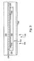
- Figure 3 shows a side view of a photodiode detector array according to one embodiment of the present invention.
- Figure 3 is a more representative rendition of a two component 2-D photodiode array with respect to the relative dimensions of the various components.
- the shield 145 is recessed in a cavity of the first substrate 210 so that the top surface of the shield is below the planar surface of the first substrate 210.
- the size of the BGA 230 in relation to the dimensions of the circuit die 160 are such that the circuit die 160 extends into the cavity of the first substrate 210.
- a further enhancement to the present invention is shown in Figure 3 as an encapsulation 310 of the circuit die 160.
- each substrate component combination 200 , 225 to be tested and verified independently.
- the circuit die represents fragile electronic components, it may be advantageous to encapsulate the circuit die 160 with a protective and in another embodiment of the present invention, an electrically insulating cover.
- the circuit die 160 is not in contact with the shield.
- the space 250 remains between the two components both thermally and electrically insulating them from each other.
- the encapsulation 310 of the circuit dies 160 add yet another level of isolation between the shield 145 and the circuit die 160 .
- an insulating layer adds increased reliability that the shield 145 will not contact the circuit die 160.
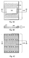
- FIG 4 shows a top, side (cross sectional) and bottom view of the first substrate component combination according to one embodiment of the present invention.
- the side view 410 of the first substrate 210 shows a recessed region 415 partially occupied by the shield 145 (note that the photodiode array is not shown in Figure 4 ).
- the first substrate is composed of 6 layers. Each layer of the substrate is capable of multiple transmission paths 270 for carrying electrical signals from the photodiode array 100 to the second substrate 220 and ultimately to the circuit die 160 .
- the top view 420 of the first substrate 210 shows a BGA 430 . Each circle represents a solder ball consistent with the description and functionality of a BGA. Note that the BGA 430 occupies only a portion of the second surface 212 of the first substrate 210 . As viewed from the top, the recessed region 415 and the shield 145 itself are shown not to possess any solder bumps associated with the BGA.
- the bottom view 440 of the first substrate shows a grid pattern 450 of contact pads consistent with the photodiode array 100 .
- Each photodiode 140 is bonded to the first substrate 210 via one of the contact pads shown in the grid pattern 450 .
- Each contact pad of the grid pattern 450 corresponds to and is connected via an electrically conductive transmission path to the BGA pattern 430 shown on the top view 420 of the first substrate 210 .
- the actual placement of the contact points for both the BGA pattern 430 and the grid pattern 450 for the photodiode array 100 may vary as will be appreciated by one skilled in the relevant art.
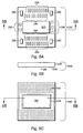
- Figure 5 shows a top, side (cross sectional) and bottom view of the second substrate component combination according to one embodiment of the present invention.
- the second substrate 220 and the circuit die 160 are shown in the various views of Figure 5 .
- the top view 520 shows a substantially planar second surface of the second substrate 220 .
- the various blocks shown on the top view 520 of the second substrate represent various passive electronic components 290 that are connected to the circuit die 160 via electrically conductive transmission paths and system interconnects 295 that connect the array to the system in which the array is implemented.
- a heat sink 525 is positioned on the second surface of the second substrate 220.
- the heat sink 525 is coupled thermally to the substrate and the circuit die 160 to control thermal expansion, contraction, and/or distortion of the second substrate 220.
- the side view 510 depicts solder bumps 230 associated with the BGA grid for connecting the second substrate 220 to the first substrate 210 and the circuit die 160 .
- the circuit die 160 is show as extending from a substantially planar first surface 222 of the second substrate 220. In other embodiments, the circuit die may be positioned in a recessed region or cavity within the second substrate 220.
- the bottom view 540 of the second substrate 220 shows a rendition of the first surface 222 of the second substrate 220 .
- the BGA pattern 550 shown on this surface corresponds directly to the BGA pattern found on the second surface 214 of the first substrate 210 (see Figure 4 ).
- Each bump of the BGA aligns a connector point located on the second surface 214 of the first substrate 210 with a receiving point located on the first surface 222 of the second substrate 222.
- Also shown in the bottom view 540 of the second substrate 220 in Figure 5 is the circuit die 160 and an encapsulating cover 310 .
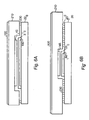
- Figure 6 shows opposing side views of one embodiment of a 2-D photodiode detector array according to one embodiment of the present invention.
- the first and second substrates 210 , 220 are not of the same dimensions.
- the second substrate 220 can be reduced in size as long as it is sufficient to house the circuit die 160 and the various passive electronic components 290 necessary for signal processing.
- various configurations of the first substrate 210 , the photodiode array 100 , the shield 145 , the second substrate 220 , and the circuit die 160 are possible without departing from the spirit and intent of the present invention.
- Figure 6 further illustrates the positioning of the shield 145 associated with the first substrate 210 in relation to the circuit die 160 associated with the second substrate 220. While the circuit die 160 is shown encapsulated 310 in this embodiment, it should be noted that a space remains between the circuit die 160 and the shield 145 and that the shield 145 is of the same dimensions or larger than the circuit die. In other embodiments of the present invention the shield 145 can be attached directly to the back of the circuit die 160 .
- Figure 7 is a flow chart for an embodiment of a method for creating a 2-D photodiode detector array according to one present invention.
- a photodiode array having two or more photodiodes is bonded 710 to a planar first surface of a first substrate so as to electrically couple each photodiode comprising the array to the first substrate.
- Electrically conductive transmission paths within the first substrate convey the electrical signals from each photodiode to the substrates' opposite second surface.
- the substrate is of sufficient rigidity to provide a distortional free structure for the photodiode array and is of a material possessing similar coefficient of thermal expansion as the photodiode array.
- a circuit die processing chip is flip chip bonded 720 to a portion of a first surface of a second substrate.
- Receiving points capable of receiving electrical signals from the photodiodes and located on another portion of the first surface of the second diode, are coupled to the circuit die via electrically conductive transmission paths within the second substrate.
- a shield, opaque to X-ray radiation is attached 730 to the opposing side of the first substrate and positioned so not to interfere with the two or more connecting points for the transmission paths from each photodiode, yet positioned so as prevent X-ray radiation from reaching the circuit die processing chip.
- Connecting points associated with the electrically conductive transmission paths of the first substrate are aligned with and electrically coupled 740 with the receiving points associated with the second substrate using BGA solder bumps.
- the first substrate and the second substrate are further aligned to interpose the shield associated with the first substrate between the circuit die of the second substrate and the incoming X-ray radiation.
- the joining of the two substrates and their various components is accomplished so as to preserve a buffering space between the shield and the circuit die for thermal and electrical isolation. Electrical signals from each photodiode are thereafter transmitted through the first substrate via the transmission paths, the BGA connection between the substrates, and the transmission paths associated with the second substrate to the circuit die.
Landscapes
- Physics & Mathematics (AREA)
- Health & Medical Sciences (AREA)
- Life Sciences & Earth Sciences (AREA)
- General Physics & Mathematics (AREA)
- High Energy & Nuclear Physics (AREA)
- Molecular Biology (AREA)
- Spectroscopy & Molecular Physics (AREA)
- Measurement Of Radiation (AREA)
- Solid State Image Pick-Up Elements (AREA)
- Light Receiving Elements (AREA)
- Apparatus For Radiation Diagnosis (AREA)
Applications Claiming Priority (2)
| Application Number | Priority Date | Filing Date | Title |
|---|---|---|---|
| US11/456,662 US7504637B2 (en) | 2006-07-11 | 2006-07-11 | Two component photodiode detector |
| PCT/US2007/072780 WO2008082689A1 (en) | 2006-07-11 | 2007-07-03 | Two component photodiode detector |
Publications (3)
| Publication Number | Publication Date |
|---|---|
| EP2041605A1 EP2041605A1 (en) | 2009-04-01 |
| EP2041605A4 EP2041605A4 (en) | 2012-01-18 |
| EP2041605B1 true EP2041605B1 (en) | 2014-04-30 |
Family
ID=38948316
Family Applications (1)
| Application Number | Title | Priority Date | Filing Date |
|---|---|---|---|
| EP07872236.0A Not-in-force EP2041605B1 (en) | 2006-07-11 | 2007-07-03 | Two component photodiode detector |
Country Status (5)
| Country | Link |
|---|---|
| US (1) | US7504637B2 (enExample) |
| EP (1) | EP2041605B1 (enExample) |
| JP (1) | JP5082064B2 (enExample) |
| IL (1) | IL196436A (enExample) |
| WO (1) | WO2008082689A1 (enExample) |
Families Citing this family (23)
| Publication number | Priority date | Publication date | Assignee | Title |
|---|---|---|---|---|
| US7535033B2 (en) * | 2004-09-14 | 2009-05-19 | Banpil Photonics, Inc. | Multicolor photodiode array and method of manufacturing |
| JP2007258199A (ja) * | 2006-03-20 | 2007-10-04 | Nec Electronics Corp | 撮像素子 |
| KR101441630B1 (ko) * | 2008-02-12 | 2014-09-23 | 삼성디스플레이 주식회사 | 엑스레이 검출기 및 이의 제조방법 |
| RU2505840C2 (ru) * | 2008-11-18 | 2014-01-27 | Конинклейке Филипс Электроникс Н.В. | Детектор спектральной визуализации |
| DE102010011582B4 (de) * | 2010-03-16 | 2011-12-01 | Siemens Aktiengesellschaft | Detektormodul für einen Strahlendetektor und Strahlendetektor |
| EP2671097B1 (en) | 2011-02-03 | 2016-10-19 | Koninklijke Philips N.V. | Single or multi-energy vertical radiation sensitive detectors |
| US8829454B2 (en) | 2012-02-27 | 2014-09-09 | Analog Devices, Inc. | Compact sensor module |
| US9116022B2 (en) | 2012-12-07 | 2015-08-25 | Analog Devices, Inc. | Compact sensor module |
| US20140348290A1 (en) * | 2013-05-23 | 2014-11-27 | General Electric Company | Apparatus and Method for Low Capacitance Packaging for Direct Conversion X-Ray or Gamma Ray Detector |
| DE102014211602B4 (de) * | 2014-06-17 | 2018-10-25 | Siemens Healthcare Gmbh | Detektormodul für einen Röntgendetektor |
| CN107003417B (zh) * | 2014-10-20 | 2019-06-21 | 模拟技术公司 | 用于辐射成像模态装置的探测器阵列的探测器单元 |
| DE102014222690B4 (de) * | 2014-11-06 | 2024-10-02 | Siemens Healthineers Ag | Detektormodul für einen Röntgendetektor |
| JP6285577B2 (ja) * | 2015-01-15 | 2018-02-28 | コーニンクレッカ フィリップス エヌ ヴェKoninklijke Philips N.V. | 撮像検出器モジュールアセンブリ |
| JP6559977B2 (ja) * | 2015-03-05 | 2019-08-14 | キヤノンメディカルシステムズ株式会社 | 検出器パック、x線ct装置 |
| US9835733B2 (en) * | 2015-04-30 | 2017-12-05 | Zhengrong Ying | Apparatus for detecting X-rays |
| US10074624B2 (en) | 2015-08-07 | 2018-09-11 | Analog Devices, Inc. | Bond pads with differently sized openings |
| US11156727B2 (en) * | 2015-10-02 | 2021-10-26 | Varian Medical Systems, Inc. | High DQE imaging device |
| US11056455B2 (en) | 2017-08-01 | 2021-07-06 | Analog Devices, Inc. | Negative fillet for mounting an integrated device die to a carrier |
| CN113228272B (zh) | 2018-12-06 | 2025-02-28 | 美国亚德诺半导体公司 | 具有无源器件组件的集成器件封装 |
| WO2020118102A1 (en) | 2018-12-06 | 2020-06-11 | Analog Devices, Inc. | Shielded integrated device packages |
| US11664340B2 (en) | 2020-07-13 | 2023-05-30 | Analog Devices, Inc. | Negative fillet for mounting an integrated device die to a carrier |
| CN116250085A (zh) * | 2020-11-13 | 2023-06-09 | Ams-欧司朗有限公司 | 用于检测x射线辐射的模块组件 |
| JP7724238B2 (ja) * | 2020-11-25 | 2025-08-15 | 浜松ホトニクス株式会社 | 撮像ユニット及び撮像システム |
Family Cites Families (7)
| Publication number | Priority date | Publication date | Assignee | Title |
|---|---|---|---|---|
| JP3957803B2 (ja) * | 1996-02-22 | 2007-08-15 | キヤノン株式会社 | 光電変換装置 |
| JP4532782B2 (ja) * | 2000-07-04 | 2010-08-25 | キヤノン株式会社 | 放射線撮像装置及びシステム |
| JP2003084066A (ja) * | 2001-04-11 | 2003-03-19 | Nippon Kessho Kogaku Kk | 放射線検出器用部品、放射線検出器および放射線検出装置 |
| US6510195B1 (en) * | 2001-07-18 | 2003-01-21 | Koninklijke Philips Electronics, N.V. | Solid state x-radiation detector modules and mosaics thereof, and an imaging method and apparatus employing the same |
| JP4133429B2 (ja) * | 2003-02-24 | 2008-08-13 | 浜松ホトニクス株式会社 | 半導体装置 |
| JP4364514B2 (ja) * | 2003-01-08 | 2009-11-18 | 浜松ホトニクス株式会社 | 配線基板、及びそれを用いた放射線検出器 |
| JP4421209B2 (ja) * | 2003-04-11 | 2010-02-24 | 浜松ホトニクス株式会社 | 放射線検出器 |
-
2006
- 2006-07-11 US US11/456,662 patent/US7504637B2/en active Active
-
2007
- 2007-07-03 JP JP2009519593A patent/JP5082064B2/ja not_active Expired - Fee Related
- 2007-07-03 EP EP07872236.0A patent/EP2041605B1/en not_active Not-in-force
- 2007-07-03 WO PCT/US2007/072780 patent/WO2008082689A1/en not_active Ceased
-
2009
- 2009-01-11 IL IL196436A patent/IL196436A/en not_active IP Right Cessation
Also Published As
| Publication number | Publication date |
|---|---|
| US7504637B2 (en) | 2009-03-17 |
| EP2041605A1 (en) | 2009-04-01 |
| JP2009544011A (ja) | 2009-12-10 |
| US20080011959A1 (en) | 2008-01-17 |
| IL196436A0 (en) | 2009-09-22 |
| WO2008082689A8 (en) | 2009-02-26 |
| WO2008082689A1 (en) | 2008-07-10 |
| IL196436A (en) | 2013-05-30 |
| JP5082064B2 (ja) | 2012-11-28 |
| EP2041605A4 (en) | 2012-01-18 |
Similar Documents
| Publication | Publication Date | Title |
|---|---|---|
| EP2041605B1 (en) | Two component photodiode detector | |
| US7572676B2 (en) | Packaging structure and method of an image sensor module | |
| US7423335B2 (en) | Sensor module package structure and method of the same | |
| US6093969A (en) | Face-to-face (FTF) stacked assembly of substrate-on-bare-chip (SOBC) modules | |
| US6525942B2 (en) | Heat dissipation ball grid array package | |
| US5789815A (en) | Three dimensional semiconductor package having flexible appendages | |
| JP2009544011A5 (enExample) | ||
| CN1180927A (zh) | 高性能低成本的多芯片组件封装件 | |
| US20230275176A1 (en) | Photon detector array assembly | |
| JP7491923B2 (ja) | シールドされた一体型デバイスパッケージ | |
| US6856027B2 (en) | Multi-chips stacked package | |
| CN110797415A (zh) | 引线组件及红外探测器 | |
| US6891275B2 (en) | Method for accommodating small minimum die in wire bonded area array packages | |
| JP4351012B2 (ja) | 半導体装置 | |
| US20060011931A1 (en) | Ic package with an integrated power source | |
| JP2005101315A (ja) | 半導体装置 | |
| JP7500876B2 (ja) | X線放射の検出のためのモジュールアセンブリ | |
| JP4799746B2 (ja) | 放射線検出器モジュール | |
| CN115332193B (zh) | 大功耗双面塑封AiP系统级封装结构及方法 | |
| CN111149208A (zh) | 集成辐射探测器设备 | |
| Fillion et al. | Advanced 3-D stacked technology | |
| JP2004088112A (ja) | マルチチップ集積モジュール | |
| CN118763081A (zh) | 光子探测器及其制备方法 | |
| Fillion et al. | Three D Vertically Stacked Electronic Structures for Array Sensors | |
| JP2000357709A (ja) | Lsiチップの実装構造 |
Legal Events
| Date | Code | Title | Description |
|---|---|---|---|
| PUAI | Public reference made under article 153(3) epc to a published international application that has entered the european phase |
Free format text: ORIGINAL CODE: 0009012 |
|
| 17P | Request for examination filed |
Effective date: 20090112 |
|
| AK | Designated contracting states |
Kind code of ref document: A1 Designated state(s): AT BE BG CH CY CZ DE DK EE ES FI FR GB GR HU IE IS IT LI LT LU LV MC MT NL PL PT RO SE SI SK TR |
|
| AX | Request for extension of the european patent |
Extension state: AL BA HR MK RS |
|
| A4 | Supplementary search report drawn up and despatched |
Effective date: 20111221 |
|
| RIC1 | Information provided on ipc code assigned before grant |
Ipc: G01T 1/24 20060101AFI20111215BHEP |
|
| DAX | Request for extension of the european patent (deleted) | ||
| 17Q | First examination report despatched |
Effective date: 20130429 |
|
| GRAP | Despatch of communication of intention to grant a patent |
Free format text: ORIGINAL CODE: EPIDOSNIGR1 |
|
| INTG | Intention to grant announced |
Effective date: 20131008 |
|
| GRAP | Despatch of communication of intention to grant a patent |
Free format text: ORIGINAL CODE: EPIDOSNIGR1 |
|
| GRAS | Grant fee paid |
Free format text: ORIGINAL CODE: EPIDOSNIGR3 |
|
| INTG | Intention to grant announced |
Effective date: 20140226 |
|
| GRAA | (expected) grant |
Free format text: ORIGINAL CODE: 0009210 |
|
| AK | Designated contracting states |
Kind code of ref document: B1 Designated state(s): AT BE BG CH CY CZ DE DK EE ES FI FR GB GR HU IE IS IT LI LT LU LV MC MT NL PL PT RO SE SI SK TR |
|
| REG | Reference to a national code |
Ref country code: GB Ref legal event code: FG4D Ref country code: CH Ref legal event code: EP |
|
| REG | Reference to a national code |
Ref country code: AT Ref legal event code: REF Ref document number: 665486 Country of ref document: AT Kind code of ref document: T Effective date: 20140515 |
|
| REG | Reference to a national code |
Ref country code: IE Ref legal event code: FG4D |
|
| REG | Reference to a national code |
Ref country code: DE Ref legal event code: R096 Ref document number: 602007036419 Country of ref document: DE Effective date: 20140612 |
|
| REG | Reference to a national code |
Ref country code: SE Ref legal event code: TRGR |
|
| REG | Reference to a national code |
Ref country code: AT Ref legal event code: MK05 Ref document number: 665486 Country of ref document: AT Kind code of ref document: T Effective date: 20140430 |
|
| REG | Reference to a national code |
Ref country code: LT Ref legal event code: MG4D |
|
| REG | Reference to a national code |
Ref country code: NL Ref legal event code: VDEP Effective date: 20140430 |
|
| PG25 | Lapsed in a contracting state [announced via postgrant information from national office to epo] |
Ref country code: CY Free format text: LAPSE BECAUSE OF FAILURE TO SUBMIT A TRANSLATION OF THE DESCRIPTION OR TO PAY THE FEE WITHIN THE PRESCRIBED TIME-LIMIT Effective date: 20140430 Ref country code: GR Free format text: LAPSE BECAUSE OF FAILURE TO SUBMIT A TRANSLATION OF THE DESCRIPTION OR TO PAY THE FEE WITHIN THE PRESCRIBED TIME-LIMIT Effective date: 20140731 Ref country code: LT Free format text: LAPSE BECAUSE OF FAILURE TO SUBMIT A TRANSLATION OF THE DESCRIPTION OR TO PAY THE FEE WITHIN THE PRESCRIBED TIME-LIMIT Effective date: 20140430 Ref country code: NL Free format text: LAPSE BECAUSE OF FAILURE TO SUBMIT A TRANSLATION OF THE DESCRIPTION OR TO PAY THE FEE WITHIN THE PRESCRIBED TIME-LIMIT Effective date: 20140430 Ref country code: IS Free format text: LAPSE BECAUSE OF FAILURE TO SUBMIT A TRANSLATION OF THE DESCRIPTION OR TO PAY THE FEE WITHIN THE PRESCRIBED TIME-LIMIT Effective date: 20140830 Ref country code: BG Free format text: LAPSE BECAUSE OF FAILURE TO SUBMIT A TRANSLATION OF THE DESCRIPTION OR TO PAY THE FEE WITHIN THE PRESCRIBED TIME-LIMIT Effective date: 20140730 Ref country code: FI Free format text: LAPSE BECAUSE OF FAILURE TO SUBMIT A TRANSLATION OF THE DESCRIPTION OR TO PAY THE FEE WITHIN THE PRESCRIBED TIME-LIMIT Effective date: 20140430 |
|
| PG25 | Lapsed in a contracting state [announced via postgrant information from national office to epo] |
Ref country code: ES Free format text: LAPSE BECAUSE OF FAILURE TO SUBMIT A TRANSLATION OF THE DESCRIPTION OR TO PAY THE FEE WITHIN THE PRESCRIBED TIME-LIMIT Effective date: 20140430 Ref country code: AT Free format text: LAPSE BECAUSE OF FAILURE TO SUBMIT A TRANSLATION OF THE DESCRIPTION OR TO PAY THE FEE WITHIN THE PRESCRIBED TIME-LIMIT Effective date: 20140430 Ref country code: LV Free format text: LAPSE BECAUSE OF FAILURE TO SUBMIT A TRANSLATION OF THE DESCRIPTION OR TO PAY THE FEE WITHIN THE PRESCRIBED TIME-LIMIT Effective date: 20140430 Ref country code: PL Free format text: LAPSE BECAUSE OF FAILURE TO SUBMIT A TRANSLATION OF THE DESCRIPTION OR TO PAY THE FEE WITHIN THE PRESCRIBED TIME-LIMIT Effective date: 20140430 |
|
| PG25 | Lapsed in a contracting state [announced via postgrant information from national office to epo] |
Ref country code: PT Free format text: LAPSE BECAUSE OF FAILURE TO SUBMIT A TRANSLATION OF THE DESCRIPTION OR TO PAY THE FEE WITHIN THE PRESCRIBED TIME-LIMIT Effective date: 20140901 |
|
| PG25 | Lapsed in a contracting state [announced via postgrant information from national office to epo] |
Ref country code: EE Free format text: LAPSE BECAUSE OF FAILURE TO SUBMIT A TRANSLATION OF THE DESCRIPTION OR TO PAY THE FEE WITHIN THE PRESCRIBED TIME-LIMIT Effective date: 20140430 Ref country code: BE Free format text: LAPSE BECAUSE OF FAILURE TO SUBMIT A TRANSLATION OF THE DESCRIPTION OR TO PAY THE FEE WITHIN THE PRESCRIBED TIME-LIMIT Effective date: 20140430 Ref country code: DK Free format text: LAPSE BECAUSE OF FAILURE TO SUBMIT A TRANSLATION OF THE DESCRIPTION OR TO PAY THE FEE WITHIN THE PRESCRIBED TIME-LIMIT Effective date: 20140430 Ref country code: SK Free format text: LAPSE BECAUSE OF FAILURE TO SUBMIT A TRANSLATION OF THE DESCRIPTION OR TO PAY THE FEE WITHIN THE PRESCRIBED TIME-LIMIT Effective date: 20140430 Ref country code: RO Free format text: LAPSE BECAUSE OF FAILURE TO SUBMIT A TRANSLATION OF THE DESCRIPTION OR TO PAY THE FEE WITHIN THE PRESCRIBED TIME-LIMIT Effective date: 20140430 Ref country code: CZ Free format text: LAPSE BECAUSE OF FAILURE TO SUBMIT A TRANSLATION OF THE DESCRIPTION OR TO PAY THE FEE WITHIN THE PRESCRIBED TIME-LIMIT Effective date: 20140430 |
|
| REG | Reference to a national code |
Ref country code: DE Ref legal event code: R097 Ref document number: 602007036419 Country of ref document: DE |
|
| PG25 | Lapsed in a contracting state [announced via postgrant information from national office to epo] |
Ref country code: LU Free format text: LAPSE BECAUSE OF FAILURE TO SUBMIT A TRANSLATION OF THE DESCRIPTION OR TO PAY THE FEE WITHIN THE PRESCRIBED TIME-LIMIT Effective date: 20140703 |
|
| REG | Reference to a national code |
Ref country code: CH Ref legal event code: PL |
|
| PLBE | No opposition filed within time limit |
Free format text: ORIGINAL CODE: 0009261 |
|
| STAA | Information on the status of an ep patent application or granted ep patent |
Free format text: STATUS: NO OPPOSITION FILED WITHIN TIME LIMIT |
|
| 26N | No opposition filed |
Effective date: 20150202 |
|
| REG | Reference to a national code |
Ref country code: IE Ref legal event code: MM4A |
|
| PG25 | Lapsed in a contracting state [announced via postgrant information from national office to epo] |
Ref country code: CH Free format text: LAPSE BECAUSE OF NON-PAYMENT OF DUE FEES Effective date: 20140731 Ref country code: LI Free format text: LAPSE BECAUSE OF NON-PAYMENT OF DUE FEES Effective date: 20140731 |
|
| REG | Reference to a national code |
Ref country code: DE Ref legal event code: R097 Ref document number: 602007036419 Country of ref document: DE Effective date: 20150202 |
|
| PG25 | Lapsed in a contracting state [announced via postgrant information from national office to epo] |
Ref country code: SI Free format text: LAPSE BECAUSE OF FAILURE TO SUBMIT A TRANSLATION OF THE DESCRIPTION OR TO PAY THE FEE WITHIN THE PRESCRIBED TIME-LIMIT Effective date: 20140430 |
|
| PG25 | Lapsed in a contracting state [announced via postgrant information from national office to epo] |
Ref country code: IE Free format text: LAPSE BECAUSE OF NON-PAYMENT OF DUE FEES Effective date: 20140703 |
|
| PG25 | Lapsed in a contracting state [announced via postgrant information from national office to epo] |
Ref country code: MC Free format text: LAPSE BECAUSE OF FAILURE TO SUBMIT A TRANSLATION OF THE DESCRIPTION OR TO PAY THE FEE WITHIN THE PRESCRIBED TIME-LIMIT Effective date: 20140430 |
|
| PG25 | Lapsed in a contracting state [announced via postgrant information from national office to epo] |
Ref country code: MT Free format text: LAPSE BECAUSE OF FAILURE TO SUBMIT A TRANSLATION OF THE DESCRIPTION OR TO PAY THE FEE WITHIN THE PRESCRIBED TIME-LIMIT Effective date: 20140430 |
|
| REG | Reference to a national code |
Ref country code: FR Ref legal event code: PLFP Year of fee payment: 10 |
|
| PG25 | Lapsed in a contracting state [announced via postgrant information from national office to epo] |
Ref country code: TR Free format text: LAPSE BECAUSE OF FAILURE TO SUBMIT A TRANSLATION OF THE DESCRIPTION OR TO PAY THE FEE WITHIN THE PRESCRIBED TIME-LIMIT Effective date: 20140430 Ref country code: HU Free format text: LAPSE BECAUSE OF FAILURE TO SUBMIT A TRANSLATION OF THE DESCRIPTION OR TO PAY THE FEE WITHIN THE PRESCRIBED TIME-LIMIT; INVALID AB INITIO Effective date: 20070703 |
|
| PGFP | Annual fee paid to national office [announced via postgrant information from national office to epo] |
Ref country code: IT Payment date: 20160727 Year of fee payment: 10 Ref country code: DE Payment date: 20160722 Year of fee payment: 10 Ref country code: GB Payment date: 20160721 Year of fee payment: 10 |
|
| PGFP | Annual fee paid to national office [announced via postgrant information from national office to epo] |
Ref country code: SE Payment date: 20160720 Year of fee payment: 10 Ref country code: FR Payment date: 20160721 Year of fee payment: 10 |
|
| REG | Reference to a national code |
Ref country code: DE Ref legal event code: R119 Ref document number: 602007036419 Country of ref document: DE |
|
| REG | Reference to a national code |
Ref country code: SE Ref legal event code: EUG |
|
| GBPC | Gb: european patent ceased through non-payment of renewal fee |
Effective date: 20170703 |
|
| REG | Reference to a national code |
Ref country code: FR Ref legal event code: ST Effective date: 20180330 |
|
| PG25 | Lapsed in a contracting state [announced via postgrant information from national office to epo] |
Ref country code: DE Free format text: LAPSE BECAUSE OF NON-PAYMENT OF DUE FEES Effective date: 20180201 Ref country code: SE Free format text: LAPSE BECAUSE OF NON-PAYMENT OF DUE FEES Effective date: 20170704 Ref country code: GB Free format text: LAPSE BECAUSE OF NON-PAYMENT OF DUE FEES Effective date: 20170703 |
|
| PG25 | Lapsed in a contracting state [announced via postgrant information from national office to epo] |
Ref country code: FR Free format text: LAPSE BECAUSE OF NON-PAYMENT OF DUE FEES Effective date: 20170731 |
|
| PG25 | Lapsed in a contracting state [announced via postgrant information from national office to epo] |
Ref country code: IT Free format text: LAPSE BECAUSE OF NON-PAYMENT OF DUE FEES Effective date: 20170703 |