EP2031546B1 - Dispositif semi-conducteur - Google Patents
Dispositif semi-conducteur Download PDFInfo
- Publication number
- EP2031546B1 EP2031546B1 EP08015142A EP08015142A EP2031546B1 EP 2031546 B1 EP2031546 B1 EP 2031546B1 EP 08015142 A EP08015142 A EP 08015142A EP 08015142 A EP08015142 A EP 08015142A EP 2031546 B1 EP2031546 B1 EP 2031546B1
- Authority
- EP
- European Patent Office
- Prior art keywords
- output
- charge pump
- circuit
- voltage
- semiconductor device
- Prior art date
- Legal status (The legal status is an assumption and is not a legal conclusion. Google has not performed a legal analysis and makes no representation as to the accuracy of the status listed.)
- Not-in-force
Links
- 239000004065 semiconductor Substances 0.000 title claims description 144
- 239000003990 capacitor Substances 0.000 claims description 17
- 239000010409 thin film Substances 0.000 claims description 13
- 230000004044 response Effects 0.000 claims description 4
- 239000010408 film Substances 0.000 description 245
- 238000000034 method Methods 0.000 description 63
- 239000010410 layer Substances 0.000 description 41
- 239000000758 substrate Substances 0.000 description 41
- XUIMIQQOPSSXEZ-UHFFFAOYSA-N Silicon Chemical compound [Si] XUIMIQQOPSSXEZ-UHFFFAOYSA-N 0.000 description 38
- 229910052710 silicon Inorganic materials 0.000 description 38
- 239000010703 silicon Substances 0.000 description 38
- 238000004891 communication Methods 0.000 description 36
- 229910052751 metal Inorganic materials 0.000 description 24
- 239000002184 metal Substances 0.000 description 24
- 239000000463 material Substances 0.000 description 23
- 230000006870 function Effects 0.000 description 22
- PXHVJJICTQNCMI-UHFFFAOYSA-N Nickel Chemical compound [Ni] PXHVJJICTQNCMI-UHFFFAOYSA-N 0.000 description 21
- 230000015572 biosynthetic process Effects 0.000 description 20
- 239000012535 impurity Substances 0.000 description 20
- 238000010586 diagram Methods 0.000 description 18
- 239000010936 titanium Substances 0.000 description 18
- 229910052581 Si3N4 Inorganic materials 0.000 description 14
- 239000000047 product Substances 0.000 description 14
- HQVNEWCFYHHQES-UHFFFAOYSA-N silicon nitride Chemical compound N12[Si]34N5[Si]62N3[Si]51N64 HQVNEWCFYHHQES-UHFFFAOYSA-N 0.000 description 14
- 239000010949 copper Substances 0.000 description 13
- KDLHZDBZIXYQEI-UHFFFAOYSA-N Palladium Chemical compound [Pd] KDLHZDBZIXYQEI-UHFFFAOYSA-N 0.000 description 12
- 229910052782 aluminium Inorganic materials 0.000 description 12
- XAGFODPZIPBFFR-UHFFFAOYSA-N aluminium Chemical compound [Al] XAGFODPZIPBFFR-UHFFFAOYSA-N 0.000 description 12
- BASFCYQUMIYNBI-UHFFFAOYSA-N platinum Chemical compound [Pt] BASFCYQUMIYNBI-UHFFFAOYSA-N 0.000 description 12
- 239000002356 single layer Substances 0.000 description 12
- 238000004544 sputter deposition Methods 0.000 description 12
- 238000005229 chemical vapour deposition Methods 0.000 description 11
- 239000011229 interlayer Substances 0.000 description 11
- 229910052750 molybdenum Inorganic materials 0.000 description 11
- 239000011733 molybdenum Substances 0.000 description 11
- 239000011347 resin Substances 0.000 description 11
- 229920005989 resin Polymers 0.000 description 11
- VYPSYNLAJGMNEJ-UHFFFAOYSA-N silicon dioxide Inorganic materials O=[Si]=O VYPSYNLAJGMNEJ-UHFFFAOYSA-N 0.000 description 11
- ZOKXTWBITQBERF-UHFFFAOYSA-N Molybdenum Chemical compound [Mo] ZOKXTWBITQBERF-UHFFFAOYSA-N 0.000 description 10
- RTAQQCXQSZGOHL-UHFFFAOYSA-N Titanium Chemical compound [Ti] RTAQQCXQSZGOHL-UHFFFAOYSA-N 0.000 description 10
- 150000004767 nitrides Chemical class 0.000 description 10
- 229910052814 silicon oxide Inorganic materials 0.000 description 10
- 229910052719 titanium Inorganic materials 0.000 description 10
- 239000010931 gold Substances 0.000 description 9
- 229910052715 tantalum Inorganic materials 0.000 description 9
- RYGMFSIKBFXOCR-UHFFFAOYSA-N Copper Chemical compound [Cu] RYGMFSIKBFXOCR-UHFFFAOYSA-N 0.000 description 8
- 229910052802 copper Inorganic materials 0.000 description 8
- 239000013078 crystal Substances 0.000 description 8
- 238000002425 crystallisation Methods 0.000 description 8
- 229910052759 nickel Inorganic materials 0.000 description 8
- 238000000206 photolithography Methods 0.000 description 8
- 230000002829 reductive effect Effects 0.000 description 8
- 229910052721 tungsten Inorganic materials 0.000 description 8
- 239000010937 tungsten Substances 0.000 description 8
- 239000000956 alloy Substances 0.000 description 7
- 230000004888 barrier function Effects 0.000 description 7
- 238000004519 manufacturing process Methods 0.000 description 7
- 238000005268 plasma chemical vapour deposition Methods 0.000 description 7
- 230000008569 process Effects 0.000 description 7
- 238000007650 screen-printing Methods 0.000 description 7
- 229910052709 silver Inorganic materials 0.000 description 7
- 239000004332 silver Substances 0.000 description 7
- GUVRBAGPIYLISA-UHFFFAOYSA-N tantalum atom Chemical compound [Ta] GUVRBAGPIYLISA-UHFFFAOYSA-N 0.000 description 7
- WFKWXMTUELFFGS-UHFFFAOYSA-N tungsten Chemical compound [W] WFKWXMTUELFFGS-UHFFFAOYSA-N 0.000 description 7
- MWUXSHHQAYIFBG-UHFFFAOYSA-N Nitric oxide Chemical compound O=[N] MWUXSHHQAYIFBG-UHFFFAOYSA-N 0.000 description 6
- BQCADISMDOOEFD-UHFFFAOYSA-N Silver Chemical compound [Ag] BQCADISMDOOEFD-UHFFFAOYSA-N 0.000 description 6
- CSDREXVUYHZDNP-UHFFFAOYSA-N alumanylidynesilicon Chemical compound [Al].[Si] CSDREXVUYHZDNP-UHFFFAOYSA-N 0.000 description 6
- 230000005540 biological transmission Effects 0.000 description 6
- 239000011651 chromium Substances 0.000 description 6
- 230000008025 crystallization Effects 0.000 description 6
- 238000009832 plasma treatment Methods 0.000 description 6
- 229910021420 polycrystalline silicon Inorganic materials 0.000 description 6
- 150000001875 compounds Chemical class 0.000 description 5
- 230000003247 decreasing effect Effects 0.000 description 5
- 238000007599 discharging Methods 0.000 description 5
- PCHJSUWPFVWCPO-UHFFFAOYSA-N gold Chemical compound [Au] PCHJSUWPFVWCPO-UHFFFAOYSA-N 0.000 description 5
- 229910052737 gold Inorganic materials 0.000 description 5
- 238000010438 heat treatment Methods 0.000 description 5
- 238000007254 oxidation reaction Methods 0.000 description 5
- 239000001301 oxygen Substances 0.000 description 5
- 229910052760 oxygen Inorganic materials 0.000 description 5
- 230000001681 protective effect Effects 0.000 description 5
- 238000000926 separation method Methods 0.000 description 5
- OKTJSMMVPCPJKN-UHFFFAOYSA-N Carbon Chemical compound [C] OKTJSMMVPCPJKN-UHFFFAOYSA-N 0.000 description 4
- OAICVXFJPJFONN-UHFFFAOYSA-N Phosphorus Chemical compound [P] OAICVXFJPJFONN-UHFFFAOYSA-N 0.000 description 4
- 229910009372 YVO4 Inorganic materials 0.000 description 4
- QVGXLLKOCUKJST-UHFFFAOYSA-N atomic oxygen Chemical compound [O] QVGXLLKOCUKJST-UHFFFAOYSA-N 0.000 description 4
- UMIVXZPTRXBADB-UHFFFAOYSA-N benzocyclobutene Chemical compound C1=CC=C2CCC2=C1 UMIVXZPTRXBADB-UHFFFAOYSA-N 0.000 description 4
- 229910052799 carbon Inorganic materials 0.000 description 4
- 229910052804 chromium Inorganic materials 0.000 description 4
- 238000005530 etching Methods 0.000 description 4
- 239000011521 glass Substances 0.000 description 4
- 229910010272 inorganic material Inorganic materials 0.000 description 4
- 239000011147 inorganic material Substances 0.000 description 4
- 238000002955 isolation Methods 0.000 description 4
- 239000010955 niobium Substances 0.000 description 4
- 239000011368 organic material Substances 0.000 description 4
- 230000003647 oxidation Effects 0.000 description 4
- 229910052763 palladium Inorganic materials 0.000 description 4
- 229910052698 phosphorus Inorganic materials 0.000 description 4
- 239000011574 phosphorus Substances 0.000 description 4
- 229910052697 platinum Inorganic materials 0.000 description 4
- 229920005591 polysilicon Polymers 0.000 description 4
- 241001465754 Metazoa Species 0.000 description 3
- 229910052779 Neodymium Inorganic materials 0.000 description 3
- 239000004952 Polyamide Substances 0.000 description 3
- 239000004642 Polyimide Substances 0.000 description 3
- NIXOWILDQLNWCW-UHFFFAOYSA-N acrylic acid group Chemical group C(C=C)(=O)O NIXOWILDQLNWCW-UHFFFAOYSA-N 0.000 description 3
- 229910021417 amorphous silicon Inorganic materials 0.000 description 3
- -1 and the like Substances 0.000 description 3
- 235000013339 cereals Nutrition 0.000 description 3
- 230000008859 change Effects 0.000 description 3
- 239000013065 commercial product Substances 0.000 description 3
- 230000005674 electromagnetic induction Effects 0.000 description 3
- 238000010894 electron beam technology Methods 0.000 description 3
- 239000007789 gas Substances 0.000 description 3
- 238000005468 ion implantation Methods 0.000 description 3
- 238000001459 lithography Methods 0.000 description 3
- 150000002739 metals Chemical class 0.000 description 3
- 239000004033 plastic Substances 0.000 description 3
- 229920002647 polyamide Polymers 0.000 description 3
- 229920001721 polyimide Polymers 0.000 description 3
- 230000001737 promoting effect Effects 0.000 description 3
- 238000011084 recovery Methods 0.000 description 3
- 229910021332 silicide Inorganic materials 0.000 description 3
- FVBUAEGBCNSCDD-UHFFFAOYSA-N silicide(4-) Chemical compound [Si-4] FVBUAEGBCNSCDD-UHFFFAOYSA-N 0.000 description 3
- 238000003860 storage Methods 0.000 description 3
- QGZKDVFQNNGYKY-UHFFFAOYSA-N Ammonia Chemical compound N QGZKDVFQNNGYKY-UHFFFAOYSA-N 0.000 description 2
- IJGRMHOSHXDMSA-UHFFFAOYSA-N Atomic nitrogen Chemical compound N#N IJGRMHOSHXDMSA-UHFFFAOYSA-N 0.000 description 2
- VYZAMTAEIAYCRO-UHFFFAOYSA-N Chromium Chemical compound [Cr] VYZAMTAEIAYCRO-UHFFFAOYSA-N 0.000 description 2
- 239000004593 Epoxy Substances 0.000 description 2
- 229910052691 Erbium Inorganic materials 0.000 description 2
- GQPLMRYTRLFLPF-UHFFFAOYSA-N Nitrous Oxide Chemical compound [O-][N+]#N GQPLMRYTRLFLPF-UHFFFAOYSA-N 0.000 description 2
- CBENFWSGALASAD-UHFFFAOYSA-N Ozone Chemical compound [O-][O+]=O CBENFWSGALASAD-UHFFFAOYSA-N 0.000 description 2
- 229910052775 Thulium Inorganic materials 0.000 description 2
- 229910052769 Ytterbium Inorganic materials 0.000 description 2
- 230000004913 activation Effects 0.000 description 2
- 238000001994 activation Methods 0.000 description 2
- 239000000853 adhesive Substances 0.000 description 2
- 230000001070 adhesive effect Effects 0.000 description 2
- 238000000137 annealing Methods 0.000 description 2
- 229910052785 arsenic Inorganic materials 0.000 description 2
- RQNWIZPPADIBDY-UHFFFAOYSA-N arsenic atom Chemical compound [As] RQNWIZPPADIBDY-UHFFFAOYSA-N 0.000 description 2
- 239000005388 borosilicate glass Substances 0.000 description 2
- 239000000919 ceramic Substances 0.000 description 2
- 238000006243 chemical reaction Methods 0.000 description 2
- 229910017052 cobalt Inorganic materials 0.000 description 2
- 239000010941 cobalt Substances 0.000 description 2
- GUTLYIVDDKVIGB-UHFFFAOYSA-N cobalt atom Chemical compound [Co] GUTLYIVDDKVIGB-UHFFFAOYSA-N 0.000 description 2
- 239000004020 conductor Substances 0.000 description 2
- 238000010168 coupling process Methods 0.000 description 2
- 229910021419 crystalline silicon Inorganic materials 0.000 description 2
- KPUWHANPEXNPJT-UHFFFAOYSA-N disiloxane Chemical class [SiH3]O[SiH3] KPUWHANPEXNPJT-UHFFFAOYSA-N 0.000 description 2
- 239000002019 doping agent Substances 0.000 description 2
- 238000001312 dry etching Methods 0.000 description 2
- 230000003203 everyday effect Effects 0.000 description 2
- 235000013305 food Nutrition 0.000 description 2
- 229910052839 forsterite Inorganic materials 0.000 description 2
- 238000007646 gravure printing Methods 0.000 description 2
- 239000012943 hotmelt Substances 0.000 description 2
- 239000011810 insulating material Substances 0.000 description 2
- 150000002500 ions Chemical class 0.000 description 2
- 238000004518 low pressure chemical vapour deposition Methods 0.000 description 2
- HCWCAKKEBCNQJP-UHFFFAOYSA-N magnesium orthosilicate Chemical compound [Mg+2].[Mg+2].[O-][Si]([O-])([O-])[O-] HCWCAKKEBCNQJP-UHFFFAOYSA-N 0.000 description 2
- 239000011572 manganese Substances 0.000 description 2
- 229910044991 metal oxide Inorganic materials 0.000 description 2
- 150000004706 metal oxides Chemical class 0.000 description 2
- 229910021421 monocrystalline silicon Inorganic materials 0.000 description 2
- 229910052758 niobium Inorganic materials 0.000 description 2
- GUCVJGMIXFAOAE-UHFFFAOYSA-N niobium atom Chemical compound [Nb] GUCVJGMIXFAOAE-UHFFFAOYSA-N 0.000 description 2
- 230000001590 oxidative effect Effects 0.000 description 2
- 238000004806 packaging method and process Methods 0.000 description 2
- 239000002245 particle Substances 0.000 description 2
- 239000005360 phosphosilicate glass Substances 0.000 description 2
- 238000007747 plating Methods 0.000 description 2
- 238000007639 printing Methods 0.000 description 2
- 230000009467 reduction Effects 0.000 description 2
- 239000010948 rhodium Substances 0.000 description 2
- 229910000679 solder Inorganic materials 0.000 description 2
- 238000000638 solvent extraction Methods 0.000 description 2
- 230000000087 stabilizing effect Effects 0.000 description 2
- 229910019655 synthetic inorganic crystalline material Inorganic materials 0.000 description 2
- MZLGASXMSKOWSE-UHFFFAOYSA-N tantalum nitride Chemical compound [Ta]#N MZLGASXMSKOWSE-UHFFFAOYSA-N 0.000 description 2
- JBQYATWDVHIOAR-UHFFFAOYSA-N tellanylidenegermanium Chemical compound [Te]=[Ge] JBQYATWDVHIOAR-UHFFFAOYSA-N 0.000 description 2
- XLYOFNOQVPJJNP-UHFFFAOYSA-N water Substances O XLYOFNOQVPJJNP-UHFFFAOYSA-N 0.000 description 2
- ZOXJGFHDIHLPTG-UHFFFAOYSA-N Boron Chemical compound [B] ZOXJGFHDIHLPTG-UHFFFAOYSA-N 0.000 description 1
- 241000196324 Embryophyta Species 0.000 description 1
- 241000282414 Homo sapiens Species 0.000 description 1
- XEEYBQQBJWHFJM-UHFFFAOYSA-N Iron Chemical compound [Fe] XEEYBQQBJWHFJM-UHFFFAOYSA-N 0.000 description 1
- PWHULOQIROXLJO-UHFFFAOYSA-N Manganese Chemical compound [Mn] PWHULOQIROXLJO-UHFFFAOYSA-N 0.000 description 1
- 229910017502 Nd:YVO4 Inorganic materials 0.000 description 1
- 240000007594 Oryza sativa Species 0.000 description 1
- 235000007164 Oryza sativa Nutrition 0.000 description 1
- KJTLSVCANCCWHF-UHFFFAOYSA-N Ruthenium Chemical compound [Ru] KJTLSVCANCCWHF-UHFFFAOYSA-N 0.000 description 1
- 229910004205 SiNX Inorganic materials 0.000 description 1
- 229910004286 SiNxOy Inorganic materials 0.000 description 1
- ATJFFYVFTNAWJD-UHFFFAOYSA-N Tin Chemical compound [Sn] ATJFFYVFTNAWJD-UHFFFAOYSA-N 0.000 description 1
- NRTOMJZYCJJWKI-UHFFFAOYSA-N Titanium nitride Chemical compound [Ti]#N NRTOMJZYCJJWKI-UHFFFAOYSA-N 0.000 description 1
- 230000002159 abnormal effect Effects 0.000 description 1
- 230000003213 activating effect Effects 0.000 description 1
- 229910045601 alloy Inorganic materials 0.000 description 1
- 229910021529 ammonia Inorganic materials 0.000 description 1
- GPBUGPUPKAGMDK-UHFFFAOYSA-N azanylidynemolybdenum Chemical compound [Mo]#N GPBUGPUPKAGMDK-UHFFFAOYSA-N 0.000 description 1
- 235000013405 beer Nutrition 0.000 description 1
- 230000008901 benefit Effects 0.000 description 1
- YXTPWUNVHCYOSP-UHFFFAOYSA-N bis($l^{2}-silanylidene)molybdenum Chemical compound [Si]=[Mo]=[Si] YXTPWUNVHCYOSP-UHFFFAOYSA-N 0.000 description 1
- 230000000903 blocking effect Effects 0.000 description 1
- 229910052796 boron Inorganic materials 0.000 description 1
- 239000000969 carrier Substances 0.000 description 1
- 230000001413 cellular effect Effects 0.000 description 1
- 230000007547 defect Effects 0.000 description 1
- 238000006356 dehydrogenation reaction Methods 0.000 description 1
- 230000000694 effects Effects 0.000 description 1
- 230000005684 electric field Effects 0.000 description 1
- 230000005611 electricity Effects 0.000 description 1
- 238000000609 electron-beam lithography Methods 0.000 description 1
- 238000001704 evaporation Methods 0.000 description 1
- 230000005284 excitation Effects 0.000 description 1
- 230000002349 favourable effect Effects 0.000 description 1
- 230000005669 field effect Effects 0.000 description 1
- 239000010419 fine particle Substances 0.000 description 1
- 239000001257 hydrogen Substances 0.000 description 1
- 229910052739 hydrogen Inorganic materials 0.000 description 1
- 125000004435 hydrogen atom Chemical class [H]* 0.000 description 1
- 238000007689 inspection Methods 0.000 description 1
- 229910052741 iridium Inorganic materials 0.000 description 1
- GKOZUEZYRPOHIO-UHFFFAOYSA-N iridium atom Chemical compound [Ir] GKOZUEZYRPOHIO-UHFFFAOYSA-N 0.000 description 1
- 238000005224 laser annealing Methods 0.000 description 1
- 238000003698 laser cutting Methods 0.000 description 1
- 230000000670 limiting effect Effects 0.000 description 1
- 239000007788 liquid Substances 0.000 description 1
- 239000004973 liquid crystal related substance Substances 0.000 description 1
- 229910052748 manganese Inorganic materials 0.000 description 1
- 239000000203 mixture Substances 0.000 description 1
- 230000004048 modification Effects 0.000 description 1
- 238000012986 modification Methods 0.000 description 1
- 150000002751 molybdenum Chemical class 0.000 description 1
- 229910021344 molybdenum silicide Inorganic materials 0.000 description 1
- 239000002105 nanoparticle Substances 0.000 description 1
- QEFYFXOXNSNQGX-UHFFFAOYSA-N neodymium atom Chemical compound [Nd] QEFYFXOXNSNQGX-UHFFFAOYSA-N 0.000 description 1
- 229910052757 nitrogen Inorganic materials 0.000 description 1
- QJGQUHMNIGDVPM-UHFFFAOYSA-N nitrogen(.) Chemical compound [N] QJGQUHMNIGDVPM-UHFFFAOYSA-N 0.000 description 1
- 230000010355 oscillation Effects 0.000 description 1
- 229910052762 osmium Inorganic materials 0.000 description 1
- SYQBFIAQOQZEGI-UHFFFAOYSA-N osmium atom Chemical compound [Os] SYQBFIAQOQZEGI-UHFFFAOYSA-N 0.000 description 1
- 230000003071 parasitic effect Effects 0.000 description 1
- 230000035515 penetration Effects 0.000 description 1
- 239000012071 phase Substances 0.000 description 1
- 230000010287 polarization Effects 0.000 description 1
- 238000005498 polishing Methods 0.000 description 1
- 239000010453 quartz Substances 0.000 description 1
- 239000002994 raw material Substances 0.000 description 1
- 230000000717 retained effect Effects 0.000 description 1
- 229910052703 rhodium Inorganic materials 0.000 description 1
- MHOVAHRLVXNVSD-UHFFFAOYSA-N rhodium atom Chemical compound [Rh] MHOVAHRLVXNVSD-UHFFFAOYSA-N 0.000 description 1
- 235000009566 rice Nutrition 0.000 description 1
- 239000010979 ruby Substances 0.000 description 1
- 229910001750 ruby Inorganic materials 0.000 description 1
- 229910052707 ruthenium Inorganic materials 0.000 description 1
- VSZWPYCFIRKVQL-UHFFFAOYSA-N selanylidenegallium;selenium Chemical compound [Se].[Se]=[Ga].[Se]=[Ga] VSZWPYCFIRKVQL-UHFFFAOYSA-N 0.000 description 1
- 230000008054 signal transmission Effects 0.000 description 1
- 239000007790 solid phase Substances 0.000 description 1
- 238000003746 solid phase reaction Methods 0.000 description 1
- 238000001228 spectrum Methods 0.000 description 1
- 239000010935 stainless steel Substances 0.000 description 1
- 229910001220 stainless steel Inorganic materials 0.000 description 1
- 230000003068 static effect Effects 0.000 description 1
- 238000007725 thermal activation Methods 0.000 description 1
- 229910021341 titanium silicide Inorganic materials 0.000 description 1
- WQJQOUPTWCFRMM-UHFFFAOYSA-N tungsten disilicide Chemical compound [Si]#[W]#[Si] WQJQOUPTWCFRMM-UHFFFAOYSA-N 0.000 description 1
- 229910021342 tungsten silicide Inorganic materials 0.000 description 1
Images


Classifications
-
- G—PHYSICS
- G06—COMPUTING; CALCULATING OR COUNTING
- G06K—GRAPHICAL DATA READING; PRESENTATION OF DATA; RECORD CARRIERS; HANDLING RECORD CARRIERS
- G06K19/00—Record carriers for use with machines and with at least a part designed to carry digital markings
- G06K19/06—Record carriers for use with machines and with at least a part designed to carry digital markings characterised by the kind of the digital marking, e.g. shape, nature, code
- G06K19/067—Record carriers with conductive marks, printed circuits or semiconductor circuit elements, e.g. credit or identity cards also with resonating or responding marks without active components
- G06K19/07—Record carriers with conductive marks, printed circuits or semiconductor circuit elements, e.g. credit or identity cards also with resonating or responding marks without active components with integrated circuit chips
- G06K19/0723—Record carriers with conductive marks, printed circuits or semiconductor circuit elements, e.g. credit or identity cards also with resonating or responding marks without active components with integrated circuit chips the record carrier comprising an arrangement for non-contact communication, e.g. wireless communication circuits on transponder cards, non-contact smart cards or RFIDs
-
- G—PHYSICS
- G06—COMPUTING; CALCULATING OR COUNTING
- G06K—GRAPHICAL DATA READING; PRESENTATION OF DATA; RECORD CARRIERS; HANDLING RECORD CARRIERS
- G06K19/00—Record carriers for use with machines and with at least a part designed to carry digital markings
- G06K19/06—Record carriers for use with machines and with at least a part designed to carry digital markings characterised by the kind of the digital marking, e.g. shape, nature, code
- G06K19/067—Record carriers with conductive marks, printed circuits or semiconductor circuit elements, e.g. credit or identity cards also with resonating or responding marks without active components
- G06K19/07—Record carriers with conductive marks, printed circuits or semiconductor circuit elements, e.g. credit or identity cards also with resonating or responding marks without active components with integrated circuit chips
- G06K19/0701—Record carriers with conductive marks, printed circuits or semiconductor circuit elements, e.g. credit or identity cards also with resonating or responding marks without active components with integrated circuit chips at least one of the integrated circuit chips comprising an arrangement for power management
- G06K19/0713—Record carriers with conductive marks, printed circuits or semiconductor circuit elements, e.g. credit or identity cards also with resonating or responding marks without active components with integrated circuit chips at least one of the integrated circuit chips comprising an arrangement for power management the arrangement including a power charge pump
Definitions
- the present invention relates to a semiconductor device.
- the present invention particularly relates to a semiconductor device capable of wireless data communication, a so-called IC chip (also referred to as an ID chip or a transponder) for RFID (radio frequency identification).
- IC chip also referred to as an ID chip or a transponder
- RFID radio frequency identification
- the semiconductor device herein means all devices that can function by utilizing the semiconductor characteristics.
- a semiconductor device receives a wireless signal transmitted from a communication device by an antenna.
- the antenna generates a signal of AC voltage (hereinafter referred to as an AC signal) by receiving the wireless signal.
- the AC signal is converted into a signal of DC voltage (hereinafter referred to as a DC signal) by a rectifier circuit which performs rectification.
- the DC signal is input to a constant voltage circuit (also referred to as a regulator or a power supply circuit) so that a power supply voltage Vdd is generated.
- the power supply voltage Vdd generated in the constant voltage circuit is applied to a plurality of circuits included in the semiconductor device.
- Patent Document 1 Japanese Published Patent Application No. 2007-43568 .
- a structure is disclosed in which, in order to increase energy efficiency of a wireless signal to be received by an antenna, a voltage of a DC signal is boosted by a boosting circuit with a charge pump, and the DC signal is supplied to an RF transmission circuit after electric power is accumulated in a charging/discharging circuit.
- a semiconductor storage device has a variable-stage charge pump, and a memory cell array to which an output from an output line of the variable-stage charge pump is fed.
- first and second charge pumps are connected in parallel between a common input bus and a common output bus.
- a first n-channel MOSFET is provided on a line connecting an output terminal of the first charge pump and the common output bus
- another n-channel MOSFET is provided on a line connecting the second charge pump and the common output bus.
- First switches are provided between the output terminal of the first charge pump and the first n-channel MOSFET, and between the input terminal of the second charge pump and the second switch.
- a second switch is provided on a line connecting an input terminal of the second charge pump and the common input bus.
- an identification (ID) tag includes a substrate having an input capable of receiving a high frequency signal.
- a first charge pump is coupled to the input and is configured to convert the high frequency signal to a substantially direct current (DC) voltage.
- a data recovery circuit is coupled to the input and is capable of recovering data from the high frequency signal.
- a back scatter switch is coupled to the input and is capable of modifying an impedance of the input, responsive to a control signal.
- a state machine is disposed on the substrate and is responsive to the data recovered by the second charge pump, where the state machine is capable of generating the control signal for the back scatter switch in response to the data.
- the DC voltage from the first charge pump is capable of providing a voltage supply for at least one of the data recovery circuit, the back scatter switch, and the state machine.
- the data recovery circuit includes a second charge pump that is capable of operating on the high frequency signal simultaneously with the first charge pump.
- the first charge pump can generate the supply voltage for the ID tag from the high frequency signal, while the second charge pump simultaneously retrieves the data from the high frequency signal.
- the first charge pump also includes a means for limiting the amplitude of the DC voltage by reducing the charge pump efficiency, once a threshold voltage is reached.
- a semiconductor device includes a capacitor element to store charge generated by receiving a wireless signal by an antenna.
- the structure of the semiconductor device including the capacitor element is effective for stabilizing power supply and accumulating electric power.
- the area or a holding voltage of the capacitor element is necessary to be increased in order to increase the amount of charge to be stored.
- to manufacture the capacitor element with an area as small as possible can achieve advantages in cost, usage and power consumption.
- a method in which voltage is boosted by a charge pump in order to increase the amount of charge to be stored and charge is stored in the capacitor element at a high voltage can be used.
- the boosting circuit with the charge pump disclosed in Patent Document 1 outputs a voltage at a last stage in the boosting circuit.
- an output voltage is uniquely determined.
- a relation between an input voltage and an output voltage which is uniquely determined by the input voltage is hard to be dealt with for the semiconductor device in which an input voltage is variable.
- electric power P supplied from a communication device changes by approximately P ⁇ 1/ r 4 .
- the semiconductor device that is capable of wireless data communication is different from general electronic devices.
- the semiconductor device that is capable of wireless data communication is used not in an environment in which constant electric power is supplied, but mainly in an environment in which electric power supply is varied depending on a communication distance.
- the semiconductor device determines a power supply voltage generated in a circuit counting on electric power supply.
- a voltage generated and supplied to a power supply circuit is increased.
- the voltage generated and supplied to the power supply circuit is decreased.
- a voltage generated in the semiconductor device has a variation depending on the distance between the semiconductor device and the communication device.
- An output of the boosting circuit is provided only at the end stage, an output voltage is uniquely determined with respect to a given input electric power.
- An object of this invention is to provide a semiconductor device that includes a booting circuit with a charge pump for efficiently using electric power supplied and can operate even if the communication distance between the communication device and the semiconductor device becomes long.
- a semiconductor device including a boosting circuit having a plurality of charge pumps for efficiently using electric power supplied is provided with a structure that adjusts an output stage of the boosting circuit.
- the semiconductor device of an embodiment of the invention includes an antenna, a plurality of charge pumps each having a diode and a capacitor element, a boosting circuit having a switch provided between the charge pumps, a reference voltage supply circuit which generates a reference voltage, and a voltage comparison circuit having a comparator.
- An output voltage from each of the plurality of charge pumps included in the boosting circuit is compared with the reference voltage by using the comparator.
- On/off of the switch of the boosting circuit are switched to control output in accordance with an output signal of the comparator.
- the semiconductor device of an embodiment of the invention includes a boosting circuit with a charge pump for efficiently using electric power supplied so that the semiconductor device of this invention can operate even if a communication distance with a communication device becomes long.
- a stage that follows a stage of the charge pumps used for predetermined boosting is not used. Since the boosting circuit does not boost a voltage to be higher than a required output voltage, a loss of electric power for boosting operation can be kept to the minimum in the boosting circuit. Therefore, the boosting circuit can be optimized and electric power consumption can be reduced.
- a semiconductor device of this invention is described with reference to a block diagram shown in FIG. 1 .
- the semiconductor device of this invention is used as a semiconductor device capable of wireless data communication, a so-called IC chip (also referred to as an ID chip, an IC chip, or a transponder) for RFID (radio frequency identification).
- IC chip also referred to as an ID chip, an IC chip, or a transponder
- RFID radio frequency identification
- a semiconductor device 100 shown in FIG. 1 includes an antenna 110, a boosting circuit 101, a reference voltage supply circuit 102, a voltage comparison circuit 103, a switch controller 104, an output changeover switch 105, and a logic circuit 106.
- the semiconductor device shown in FIG 1 transmits and receives signals and receives radio waves that serve as electric power source by the antenna 110.
- the boosting circuit 101 has a function of generating a voltage from the radio wave received and generating a voltage higher than a power supply voltage of the semiconductor device.
- the reference voltage supply circuit 102 is a circuit for obtaining a constant output voltage by stepping down an input voltage and has a function of generating a reference voltage to be input to the voltage comparison circuit 103.
- the voltage comparison circuit 103 has a function of comparing the reference voltage generated in the reference voltage supply circuit 102 and a voltage based on an output voltage from each of a plurality of charge pumps included in the boosting circuit 101 and generating a logic signal (also referred to as an output signal) which is a result from comparison of voltages, and a function of controlling on/off of a switch provided in the boosting circuit 101.
- the switch controller 104 has a function of outputting a control signal for controlling on/off of the output changeover switch 105 on the basis of the logic signal which is the result from comparison in the voltage comparison circuit 103.
- the output changeover switch 105 includes a plurality of switches, and on/off of which switch is controlled in accordance with the control signal output from the switch controller 104.
- the same number of switches as that of the plurality of charge pumps included in the boosting circuit 101 is required for the output changeover switch 105.
- the output voltage of the boosting circuit 101 which is selected by the output changeover switch 105 is supplied to the logic circuit 106.
- the logic circuit 106 may have any structure as long as it functions as a semiconductor device; for example, a structure including a demodulation circuit, a modulation circuit, a CPU (central processing unit), a ROM (read only memory), and a RAM (random access memory) may be employed. In operation of the logic circuit 106, the signal received by the antenna 110 is boosted by the boosting circuit 101.
- the boosted signal is demodulated by a demodulation circuit in the logic circuit and a CPU, a ROM, and a RAM performs arithmetic processing or reading-out in accordance with data corresponding to a command.
- the data subjected to the arithmetic processing or read out by the CPU, the ROM, and the RAM is demodulated in the demodulation circuit and is transmitted to the communication device by the antenna 110.
- an electromagnetic coupling method As a transmission method of a signal that can be applied to the antenna 110 in the semiconductor device 100, an electromagnetic coupling method, an electromagnetic induction method, a microwave method, or the like can be employed. A practitioner may select a transmission method in consideration of use as appropriate and an antenna with an appropriate length and shape with respect to the transmission method is provided.
- a conductive film which functions as an antenna is formed into a circular shape (e.g., a loop antenna) or a spiral shape (e.g., a spiral antenna) to utilize electromagnetic induction due to changes in electric field density.
- the length or the shape of the conductive film functioning as the antenna may be set as appropriate in consideration of a wavelength of a radio wave used for signal transmission.
- the conductive film functioning as the antenna can be formed into a linear shape (e.g., a dipole antenna), a flat shape (e.g., a patch antenna), or the like.
- the shape of the conductive film functioning as an antenna is not limited to a linear shape but may be a curved shape, a meandering shape, or a combination thereof in consideration of the wavelength of an electromagnetic wave.
- the semiconductor device and the communication device communicate by one-way communication or two-way communication, employing any one of a space division multiplex method, a polarization division multiplex method, a frequency division multiplex method, a time division multiplex method, a code division multiplex method, or an orthogonal frequency division multiplex method.
- any of the following may be employed: higher than or equal to 300 GHz and lower than 3 THz, which is the frequency of a submillimeter wave; higher than or equal to 30 GHz and lower than 300 GHz, which is the frequency of a millimeter wave; higher than or equal to 3 GHz and lower than 30 GHz, which is the frequency of a microwave; higher than or equal to 300 MHz and lower than 3 GHz, which is the frequency of an ultrahigh frequency wave; higher than or equal to 30 MHz and lower than 300 MHz, which is the frequency of a very high frequency wave; higher than or equal to 3 MHz and lower than 30 MHz, which is the frequency of a short wave; higher than or equal to 300 kHz and lower than 3 MHz, which is the frequency of a medium wave; higher than or equal to 30 kHz and lower than 300 kHz, which is the frequency of a long wave; and higher than or equal to 3 kHz and lower than 30 kHz, which
- a carrier wave of the semiconductor device and the communication device may be modulated by either analog modulation or digital modulation, and any one of amplitude modulation, phase modulation, frequency modulation, or spread spectrum modulation may be employed. It is preferable that the amplitude modulation or the frequency modulation be used.
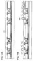
- FIG 2 shows a structure of a boosting circuit with four stages provided with four charge pumps as an example.
- This invention is not limited to the boosting circuit with four stages provided with four charge pumps and may be a boosting circuit with n stages (n is a natural number of 2 or more) provided with n charge pumps.
- the boosting circuit 101 shown in FIG. 2 includes an input wiring 200, a first charge pump 201, a second charge pump 202, a third charge pump 203, a fourth charge pump 204, a first n-channel transistor 205, and a second n-channel transistor 206.
- the input wiring 200 to which output from the antenna 110 is input is electrically connected to input terminals of the first to fourth charge pumps 201 to 204.
- An output terminal of the first charge pump 201 is electrically connected to the input terminal of the second charge pump 202.
- An output terminal of the second charge pump 202 is electrically connected to a first terminal of the first n-channel transistor 205.
- a second terminal of the first n-channel transistor 205 is electrically connected to the input terminal of the third charge pump 203.
- An output terminal of the third charge pump 203 is electrically connected to a first terminal of the second n-channel transistor 206.
- a second terminal of the second n-channel transistor 206 is electrically connected to the input terminal of the fourth charge pump 204.
- An output terminal of the fourth charge pump 204 is electrically connected to the output changeover switch 105.
- a first output wiring 223, a second output wiring 224, a third output wiring 225, and a fourth output wiring 226 that output output voltages from the first to fourth charge pumps 201 to 204 are electrically connected to the output changeover switch 105.
- Gates of the first n-channel transistor 205 and the second n-channel transistor 206 are electrically connected to an output wiring 418 and an output wiring 419, respectively, of the voltage comparison circuit 103 in order to control on/off of the transistors.
- the first n-channel transistor 205 and the second n-channel transistor 206 function as switches that change the number of stages of the charge pumps in the boosting circuit 101.
- the first n-channel transistor 205 and the second n-channel transistor 206 are the switches that change the number of charge pumps actually used for boosting voltage in the plurality of charge pumps in the boosting circuit 101.
- the first n-channel transistor 205 and the second n-channel transistor 206 also function as switches that change the number of output stages in the boosting circuit 101.
- Gates of the first n-channel transistor 205 and the second n-channel transistor 206 are electrically connected to the output wiring 418 and the output wiring 419, respectively, of the voltage comparison circuit 103.
- the gate of the first n-channel transistor 205 opens or closes a channel between the first terminal and the second terminal of the first n-channel transistor 205 in response to a signal from the output wiring 418 in the voltage comparison circuit 103
- the gate of the second n-channel transistor 206 opens or closes a channel between the first terminal and the second terminal of the second n-channel transistor 206 in response to a signal from the output wiring 419 in the voltage comparison circuit 103.
- a switch provided between each of the plurality of charge pumps may be provided for every plurality of charge pumps or every single charge pump. When one switch is provided for the plurality of charge pumps, the number of switches can be reduced and the semiconductor device can be downsized. Alternatively, when the switch is provided for every charge pump, a predetermined output voltage can be easily obtained.
- a transistor is an element having at least three terminals of a gate, a drain, and a source.
- the transistor has a channel between the drain and the source, and current can flow through the drain, the channel, and the source.
- a region functioning as a source and a drain may not be called the source or the drain in some cases. In that case, they are referred to as a first terminal or a second terminal, for example.
- the first to fourth charge pumps 201 to 204 included in the boosting circuit 101 shown in FIG. 2 each include a first capacitor element 207, a second capacitor element 208, a first diode 215, and a second diode 216 by way of example.
- a first electrode of the first capacitor element 207 is electrically connected to the input wiring 200.
- a second electrode of the first capacitor element 207 is electrically connected to a second electrode of the first diode 215 and a first electrode of the second diode 216.
- a first electrode of the first diode 215 is electrically connected to ground potential.
- the second diode 216 is electrically connected to the first electrode of the first diode 215 in the second charge pump.
- a second electrode of the second diode 216 is electrically connected to the first electrode of the first diode 215 in the third charge pump through the first n-channel transistor 205.
- a second electrode of the second diode 216 is electrically connected to the first electrode of the first diode 215 in the fourth charge pump through the second n-channel transistor 206.
- a first electrode of the second capacitor element 208 is electrically connected to the second electrode of the second diode 216 which is an output of the first charge pump, and a second electrode of the second capacitor element 208 is electrically connected to the ground potential.
- the capacitor elements shown in FIG 2 each have an electrical connection using two terminals. In that case, one electrode of each of the capacitor elements is called a first electrode and the other electrode is called a second electrode. Further, the diodes shown in FIG 2 each have an electrical connection using two terminals. In that case, an anode of each of the diodes is called a first electrode and a cathode of each of the diodes is called a second electrode.
- the charge pump is a circuit having a function of outputting a higher voltage than a voltage to be input.
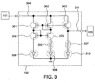
- FIG 3 shows a structural example of the reference voltage supply circuit 102 shown in FIG. 1 .
- the charge pump operates as a rectifier circuit. Since the semiconductor device is supplied with electric power through an electromagnetic wave with high frequency from the communication device, electromotive force obtained in the antenna 110 is AC voltage. Output of the first charge pump 201 is input to the reference voltage supply circuit 102 as source of voltage supply because a rectified DC voltage is necessary for the reference voltage supply circuit 102.
- the reference voltage supply circuit 102 includes an input wiring 300, a first p-channel transistor 301, a second p-channel transistor 302, a third p-channel transistor 303, a first n-channel transistor 304, a second n-channel transistor 305, a first resistor element 306, a second resistor element 307, a first diode 308, a second diode 309, and a third diode 310.
- the input wiring 300 to which an output voltage is input from the boosting circuit 101 is electrically connected to the output wiring 223 of the first charge pump.
- the input wiring 300 is electrically connected to a first terminal of each of the first to third p-channel transistors 301 to 303.
- a gate electrode of each of the first p-channel transistor 301 and the second p-channel transistor 302 is electrically connected to a second terminal of the second p-channel transistor 302.
- a second terminal of the first p-channel transistor 301 is electrically connected to a first terminal and a gate electrode of the first n-channel transistor 304 and a gate electrode of the second n-channel transistor 305.
- a first terminal of the second n-channel transistor 305 is electrically connected to a second terminal of the second p-channel transistor 302, and a second terminal of the second n-channel transistor 305 is electrically connected to ground potential through the first resistor element 306 and the second diode 309.
- a second terminal of the first n-channel transistor 304 is electrically connected to the ground potential through the first diode 308.
- a second terminal of the third p-channel transistor 303 is electrically connected to the output wiring 311, and the ground potential through the second resistor element 307 and the third diode 310.
- a second electrode of each of the first to third diodes 308 to 310 is electrically connected to the ground potential.
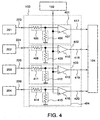
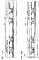
- FIG 4 shows a structural example of the voltage comparison circuit 103 shown in FIG 1 .
- the voltage comparison circuit 103 shown in FIG. 4 includes a first voltage comparison circuit 401, a second voltage comparison circuit 402, a third voltage comparison circuit 403, and a fourth voltage comparison circuit 404 which correspond to the number of the plurality of charge pumps included in the boosting circuit 101. Then, input terminals of the first to fourth voltage comparison circuit 401 to 404 are electrically connected to the output wiring 223 of the first charge pump 201, the output wiring 224 of the second charge pump 202, the output wiring 225 of the third charge pump 203, and the output wiring 226 of the fourth charge pump 204, respectively.
- an output wiring 417 of the first voltage comparison circuit 401, an output wiring 418 of the second voltage comparison circuit 402, an output wiring 419 of the third voltage comparison circuit 403, and an output wiring 420 of the fourth voltage comparison circuit 404 are electrically connected to the switch controller 104.
- the first voltage comparison circuit 401 includes a first resistor element 405, a second resistor element 406, and a first comparator 407.
- the first resistor element 405 is electrically connected to the output wiring 223 of the first charge pump 201, the second resistor element 406, and an inverting input terminal of the first comparator 407.
- the second resistor element 406 is grounded.
- a non-inverting input terminal of the first comparator 407 is electrically connected to an output of the reference voltage supply circuit 102. Note that a voltage obtained by dividing an output voltage from the first charge pump 201 by the first resistor element 405 and the second resistor element 406 is denoted as a voltage V _1 which is based on the output voltage from the first charge pump 201.
- the second voltage comparison circuit 402 includes a third resistor element 408, a fourth resistor element 409, and a second comparator 410.
- the third resistor element 408 is electrically connected to the output wiring 224 of the second charge pump 202, the fourth resistor element 409, and an inverting input terminal of the second comparator 410.
- a non-inverting input terminal of the second comparator 410 is electrically connected to an output of the reference voltage supply circuit 102.
- the third voltage comparison circuit 403 includes a fifth resistor element 411, a sixth resistor element 412, and a third comparator 413.
- the fifth resistor element 411 is electrically connected to the output wiring 225 of the third charge pump 203, the sixth resistor element 412, and an inverting input terminal of the third comparator 413.
- a non-inverting input terminal of the third comparator 413 is electrically connected to the output of the reference voltage supply circuit 102.
- the fourth voltage comparison circuit 404 includes a seventh resistor element 414, an eighth resistor element 415, and a fourth comparator 416.
- the seventh resistor element 414 is electrically connected to the output wiring 226 of the fourth charge pump 204, the eighth resistor element 415, and an inverting input terminal of the fourth comparator 416.
- a non-inverting input terminal of the fourth comparator 416 is electrically connected to the output of the reference voltage supply circuit 102.
- a voltage obtained by dividing an output voltage from the second charge pump 202 by the third resistor element 408 and the fourth resistor element 409 is denoted as a voltage V _2 which is based on the output voltage from the second charge pump 202.
- a voltage obtained by dividing an output voltage from the third charge pump 203 by the fifth resistor element 411 and the sixth resistor element 412 is denoted as a voltage V _3 which is based on the output voltage from the third charge pump 203.
- a voltage obtained by dividing an output voltage from the fourth charge pump 204 by the seventh resistor element 414 and the eighth resistor element 415 is denoted as a voltage V _4 which is based on the output voltage from the fourth charge pump 204.
- gate electrodes of the first n-channel transistor 205 and the second n-channel transistor 206 for switching an output stage of the boosting circuit 101 are connected to the output wiring 418 of the second voltage comparison circuit 402 and the output wiring 419 of the third voltage comparison circuit 403, respectively, as described above.
- An n-channel transistor is not provided between the first charge pump 201 and the second charge pump 202 in the boosting circuit 101 shown in FIG. 2 in order to secure the output voltage of the boosting circuit 101.
- the switch controller 104 that changes the output stage of the boosting circuit 101 uses a voltage based on an output voltage of a stage which is a next stage of the output stage, as a control signal for selecting the output stage of the charge pump.
- the output voltage of the second charge pump 202 is always necessary to be monitored by the voltage comparison circuit 103. Therefore, a switch using a transistor or the like does not need to be provided between the first charge pump 201 and the second charge pump 202 for electrical isolation. Thus, operation is possible without providing an n-channel transistor between the first charge pump 201 and the second charge pump 202, whereby an effect such as reduction in the number of transistors can be achieved in this embodiment mode.
- N is a natural number
- a voltage output from the output wiring 223 of the first charge pump 201 is input to the first voltage comparison circuit 401, the first comparator 407 compares an intermediate voltage ( V _1), which is divided by the first resistor element 405 and the second resistor element 406, of a node between them, with a voltage ( V ref) supplied from the reference voltage supply circuit 102, and an output signal of the first comparator 407 is determined in accordance with a magnitude relation of these voltages.
- output signals from the second comparator 410, the third comparator 413, and the fourth comparator 416 are determined in accordance with V _2 to V _4 and V ref.
- Output from the first to fourth comparators are digital signals of "high” (also referred to as a high potential signal or simply, an H signal) or "low” (also referred to as a low potential signal or simply, an L signal).
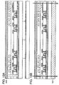
- FIG 5 shows a structural example of the switch controller 104 shown in FIG 1 .
- the switch controller 104 shown in FIG 5 includes a first Exclusive-OR (Ex-OR) circuit 501, a second Ex-OR circuit 502, and a third Ex-OR circuit 503.
- the Ex-OR circuits output an L signal when two input signals are the same and output an H signal when two input signals are different.
- the output wiring 417 of the first voltage comparison circuit 401 and the output wiring 418 of the second voltage comparison circuit 402 are electrically connected to terminals on an input side of the first Ex-OR circuit 501.
- the output wiring 418 of the second voltage comparison circuit 402 and the output wiring 419 of the third voltage comparison circuit 403 are electrically connected to terminals on an input side of the second Ex-OR circuit 502.
- the output wiring 419 of the third voltage comparison circuit 403 and the output wiring 420 of the fourth voltage comparison circuit 404 are electrically connected to terminals on an input side of the third Ex-OR circuit 503.
- first to fourth controller output wirings 504 to 507 to which a signal of the output wiring 420 of the fourth voltage comparison circuit 404 and output signals of the first to third Ex-OR circuits 501 to 503 are output from the switch controller 104, are electrically connected to the output changeover switch 105.
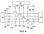
- FIG 6 shows a structural example of the output changeover switch 105 shown in FIG. 1 .
- the output changeover switch 105 includes a third n-channel transistor 601, a fourth n-channel transistor 602, a fifth n-channel transistor 603, and a sixth n-channel transistor 604.
- a first terminal of the third n-channel transistor 601 is electrically connected to the output wiring 223 of the first charge pump 201, a second terminal of the third n-channel transistor 601 is electrically connected to the first output wiring 605, and a gate of the third n-channel transistor 601 is electrically connected to the first controller output wiring 504.
- a first terminal of the fourth n-channel transistor 602 is electrically connected to the output wiring 224 of the second charge pump 202, a second terminal of the fourth n-channel transistor 602 is electrically connected to the second output wiring 606, and a gate of the fourth n-channel transistor 602 is electrically connected to the second controller output wiring 505.
- a first terminal of the fifth n-channel transistor 603 is electrically connected to the output wiring 225 of the third charge pump 203, a second terminal of the fifth n-channel transistor 603 is electrically connected to the third output wiring 607, and a gate of the fifth n-channel transistor 603 is electrically connected to the third controller output wiring 506.
- a first terminal of the sixth n-channel transistor 604 is electrically connected to the output wiring 226 of the fourth charge pump 204, a second terminal of the sixth n-channel transistor 604 is electrically connected to the fourth output wiring 608, and a gate of the sixth n-channel transistor 604 is electrically connected to the fourth controller output wiring 507.
- the third to sixth n-channel transistors 601 to 604 function as opening or closing switches that determine whether output voltages from the first to fourth charge pumps 201 to 204 are input to the logic circuit 106 or not.
- the output stage is always only one selected stage.
- the semiconductor device receives a receive signal transmitted from the communication device by the antenna.
- electric power output from the communication device is constant, electric power obtained through the receive signal depends on a distance between the communication device and the semiconductor device. Thus, the shorter the distance becomes, the larger the amount of the electric power to be supplied to the semiconductor device becomes.
- the number of stages of the charge pumps in the boosting circuit (the number of charge pumps actually used for boosting voltage among the plurality of charge pumps in the boosting circuit 101) is changed when the switch controller 104 selects an appropriate output stage in accordance with a result from comparison of the reference voltage V ref with each output from the first to fourth charge pumps 201 to 204 in the voltage comparison circuit.
- the output stage of the boosting circuit is selected in accordance with a communication distance at that time and an appropriate output voltage can be obtained.
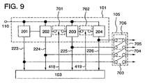
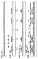
- FIGS. 7A and 7B , FIGS. 8A and 8B , and FIG. 9 show the first charge pump 201, the second charge pump 202, the third charge pump 203, the fourth charge pump 204, a first switch 701, a second switch 702, a third switch 703, a fourth switch 704, a fifth switch 705, a sixth switch 706, the output wiring 223 of the first charge pump, the output wiring 224 of the second charge pump, the output wiring 225 of the third charge pump, and the output wiring 226 of the fourth charge pump. Since FIGS.
- FIGS. 7A and 7B , FIGS. 8A and 8B , and FIG. 9 are diagrams for describing on/off operation of each switch, circuits and the like about the boosting circuit are not shown in detail. Moreover, in FIGS. 7A and 7B , FIGS. 8A and 8B , and FIG. 9 , in order to express electrical connection of n-channel transistors, the n-channel transistors are denoted as switches and the electrical connection is described by on/off of the switches.
- the first to fourth charge pumps 201 to 204 are electrically connected to the antenna 110.
- the first charge pump 201 is electrically connected to the second charge pump 202.
- the second charge pump 202 is electrically connected to the third charge pump 203 through the first switch 701.
- the third charge pump 203 is electrically connected to the fourth charge pump 204 through the second switch 702.
- the output wirings 223 to 226 of the first to fourth charge pumps 201 to 204 are electrically connected to the third to sixth switches 703 to 706, respectively.
- an output voltage of a charge pump in an n-th stage is denoted as Vn and the output voltage of the reference voltage supply circuit is denoted as V ref.
- Vn the output voltage of the reference voltage supply circuit
- V ref the output voltage of the reference voltage supply circuit
- the first switch 701 and the second switch 702 Since a signal for controlling on/off of the first switch 701 is the same as the signal from the output wiring 418 of the second comparator 410, and a signal for controlling on/off of the second switch 702 is the same as the signal from the output wiring 419 of the third comparator 413, the first switch 701 and the second switch 702 to which the L signals are input are turned off. Therefore, the third charge pump 203 and the fourth charge pump 204 are not electrically connected to the first charge pump 201 and the second charge pump 202 and not supplied with electric power, whereby the output voltages from the third charge pump 203 and the fourth charge pump 204 cannot be obtained. Moreover, in the switch controller 104 described in FIG.
- the first controller output wiring 504 outputs an H signal and the second to fourth controller output wirings 505 to 507 output L signals.
- the third switch 703 is turned on and the fourth to sixth switches 704 to 706 are turned off. Therefore, only the output voltage V 1 from the first charge pump 201 can be obtained.
- the third charge pump 203 is electrically connected to the first charge pump 201 and the second charge pump 202 so that the output voltage can be obtained. That is, the output voltage from the third charge pump 203 is obtained by switching the output stage of the boosting circuit when the distance between the semiconductor device and the communication device is changed and the electric power supply is increased or decreased.
- the fourth charge pump 204 is not electrically connected to the first to third charge pumps 201 to 203 and not supplied with electric power, whereby the output voltage from the fourth charge pump 204 cannot be obtained.
- the second controller output wiring 505 outputs an H signal and the first controller output wiring 504, the third controller output wiring 506, and the fourth controller output wiring 507 output L signals.
- the fourth switch 704 is turned on and the third switch 703, the fifth switch 705, and the sixth switch 706 are turned off. Therefore, only an output voltage V 2 from the second charge pump 202 can be obtained.
- the signal for controlling on/off of the first switch 701 is the same as the signal from the output wiring 418 of the second comparator 410, and the signal for controlling on/off of the second switch 702 is the same as the signal from the output wiring 419 of the third comparator 413, the first switch 701 and the second switch 702 to which the H signals are input are turned on. Therefore, the third charge pump 203 and the fourth charge pump 204 are electrically connected to the first charge pump 201 and the second charge pump 202 so that the output voltages can be obtained. That is, the output voltage from the fourth charge pump 204 is obtained by switching the output stage of the boosting circuit when the distance between the semiconductor device and the communication device is changed and the electric power supply is increased or decreased.
- the third controller output wiring 506 outputs an H signal and the first controller output wiring 504, the second controller output wiring 505, and the fourth controller output wiring 507 output L signals.
- the fifth switch 705 is turned on and the third switch 703, the fourth switch 704 and the sixth switch 706 are turned off. Therefore, only the output voltage V 3 from the third charge pump 203 can be obtained.
- the third charge pump 203 and the fourth charge pump 204 are electrically connected to the first charge pump 201 and the second charge pump 202 so that the output voltages can be obtained. That is, the output voltage from the fourth charge pump 204 is obtained by switching the output stage of the boosting circuit when the distance between the semiconductor device and the communication device is changed and the electric power supply is increased or decreased.
- the fourth controller output wiring 507 outputs an H signal and the first to third controller output wirings 504 to 506 output L signals.
- the sixth switch 706 is turned on and the third switch 703, the fourth switch 704, and the fifth switch 705 are turned off. Therefore, only the output voltage V 4 from the fourth charge pump 204 can be obtained.
- the number of outputs can be increased or decreased by changing the structure of the logic circuit in the switch controller 104.
- the resistance ratio of two resistor elements in the voltage comparison circuit is changed, voltage for comparison in the charge pump varies; therefore, in order to adjust the voltage for comparison, the resistance value may be changed.
- the output stage of the boosting circuit corresponds to the charge pump that is at the last stage of the plurality of charge pumps actually used for boosting voltage.
- each of the first charge pump 201 in FIG. 7B , the second charge pump 202 in FIG. 8A , the third charge pump 203 in FIG. 8B , and the fourth charge pump 204 in FIG. 9 corresponds to the output stage in the boosting circuit 101.
- a voltage value which depends on the distance between the semiconductor device and the communication device can be controlled at a constant value; this can reduce a loss of electric power in the boosting circuit in the semiconductor device and expand a range of operable distance.
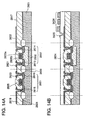
- a mode is particularly described in which a semiconductor device is provided with a transistor fabricated using a semiconductor film formed over an insulating substrate is formed.
- a release layer 1902 is formed on one surface of a substrate 1901, and then an insulating film 1903 to be a base and an amorphous semiconductor film 1904 (for example, a film containing amorphous silicon) are formed ( FIG. 10A ).
- the release layer 1902, the insulating film 1903, and the amorphous semiconductor film 1904 can be successively formed. Being formed successively, they are not exposed to the air and thus mixture of an impurity can be prevented.
- a glass substrate, a quartz substrate, a metal substrate, a stainless steel substrate, a plastic substrate which has heat resistance to a process temperature in the process, or the like is preferably used.
- Such a substrate has no significant limitation on its area or its shape.
- productivity can be significantly increased.
- Such a merit is greatly advantageous as compared to a case of using a circular silicon substrate. Therefore, even in a case of forming an integrated circuit portion or an antenna larger, the cost can be low as compared to the case of using a silicon substrate.
- the release layer 1902 may be selectively formed as necessary by a photolithography method after a release layer is formed over an entire surface of the substrate 1901. Further, while the release layer 1902 is formed so as to be in contact with the substrate 1901, it is also allowed that an insulating film such as a silicon oxide (SiO x ) film, a silicon oxynitride (SiO x N y ) (x > y) film, a silicon nitride (SiN x ) film, or a silicon nitride oxide (SiN x O y ) ( x > y ) film is formed and the release layer 1902 is formed so as to be in contact with the insulating film, as necessary.
- an insulating film such as a silicon oxide (SiO x ) film, a silicon oxynitride (SiO x N y ) (x > y) film, a silicon nitride (SiN x ) film, or
- a metal film, a layered structure of a metal film and a metal oxide film, or the like can be used as the release layer 1902.
- the metal film is formed to have a single-layer structure or a layered structure of a film formed of an element selected from tungsten (W), molybdenum (Mo), titanium (Ti), tantalum (Ta), niobium (Nb), nickel (Ni), cobalt (Co), zirconium (Zr), zinc (Zn), ruthenium (Ru), rhodium (Rh), palladium (Pd), osmium (Os), or iridium (Ir), or an alloy material or a compound material including any of the above elements as its main component.
- the metal film can be formed by a sputtering method, various CVD methods such as a plasma CVD method, or the like.
- a sputtering method various CVD methods such as a plasma CVD method, or the like.
- an oxide or oxynitride of the metal film can be formed on the surface of the metal film by performing plasma treatment in an oxygen atmosphere or an N 2 O atmosphere, or heat treatment in an oxygen atmosphere or an N 2 O atmosphere.
- a metal film is formed and then a surface thereof is treated with a highly oxidative solution such as an ozone solution, so that an oxide or oxynitride of the metal film can be formed on the surface of the metal film.
- the insulating film 1903 is formed to have a single-layer structure or a layered structure of a film containing oxide of silicon or nitride of silicon by a sputtering method, a plasma CVD method, or the like.
- a silicon nitride oxide film may be formed for a first layer
- a silicon oxynitride film may be formed for a second layer, for example.
- a silicon oxide film, a silicon nitride oxide film, and a silicon oxynitride film may be formed for a first layer, a second layer, and a third layer, respectively.
- a silicon oxynitride film, a silicon nitride oxide film, and a silicon oxynitride film may be formed for a first layer, a second layer, and a third layer, respectively.
- the insulating film to be a base functions as a blocking film for preventing impurities from entering from the substrate 1901.
- the semiconductor film 1904 is formed to a thickness of from 25 to 200 nm (preferably, from 30 to 150 nm) by a sputtering method, an LPCVD method, a plasma CVD method, or the like.
- a sputtering method preferably, from 30 to 150 nm
- an amorphous silicon film may be formed, for example.
- the amorphous semiconductor film 1904 is crystallized by laser light irradiation.
- the amorphous semiconductor film 1904 may be crystallized by a method in which laser light irradiation is combined with a thermal crystallization method using an RTA or an annealing furnace, or a thermal crystallization method using a metal element for promoting crystallization, or the like.
- the obtained crystalline semiconductor film is etched so as to have a desired shape, so that semiconductor films 1904a to 1904d are formed.
- a gate insulating film 1905 is formed so as to cover the semiconductor films 1904a to 1904d (see FIG. 10B ).
- an amorphous semiconductor film for example, an amorphous silicon film
- a plasma CVD method a solution containing nickel that is a metal element for promoting crystallization is retained on the amorphous semiconductor film, and a dehydrogenation treatment (at 500°C, for one hour) and a thermal crystallization treatment (at 550°C, for four hours) are performed on the amorphous semiconductor film, so that a crystalline semiconductor film is formed.
- the crystalline semiconductor film is irradiated with laser light from a laser oscillator, and a photolithography method is used, so that the semiconductor films 1904a to 1904d are formed.
- the amorphous semiconductor film may be crystallized only by laser light irradiation.
- a continuous wave laser beam (a CW laser beam) or a pulsed wave laser beam (a pulsed laser beam) can be used.
- a laser beam which can be used here a laser beam emitted from one or more of the following can be used: a gas laser such as an Ar laser, a Kr laser, or an excimer laser; a laser of which medium is single crystalline YAG, YVO 4 , forsterite (Mg 2 SiO 4 ), YAlO 3 , or GdVO 4 , or polycrystalline (ceramic) YAG, Y 2 O 3 , YVO 4 , YAlO 3 , or GdVO 4 , added with one or more of Nd, Yb, Cr, Ti, Ho, Er, Tm, and Ta as a dopant; a glass laser; a ruby laser; an alexandrite laser; a Ti:sapphire laser; a copper vapor laser; and a gold vapor laser.
- the second harmonic (532 nm) or the third harmonic (355 nm) of an Nd:YVO 4 laser (fundamental wave of 1064 nm) can be used.
- a power density of approximately 0.01 to 100 MW/cm 2 (preferably, 0.1 to 10 MW/cm 2 ) is necessary. Irradiation is conducted at a scanning rate of approximately 10 to 2000 cm/sec.
- a laser beam is oscillated at a repetition rate of higher than or equal to 10 MHz
- the semiconductor film is irradiated with a next pulse. Therefore, unlike a case of using a pulsed laser with a low repetition rate, a solid-liquid interface can be continuously moved in the semiconductor film, so that crystal grains which continuously grow in a scanning direction can be obtained.
- a gate insulating film 1905 which covers the semiconductor films 1904a to 1904d is formed.
- the gate insulating film 1905 is formed to have a single-layer structure or a layered structure of a film containing oxide of silicon or nitride of silicon by a CVD method, a sputtering method, or the like.
- the gate insulating film 1905 is formed to have a single-layer structure or a layered structure of a silicon oxide film, a silicon oxinitride film, or a silicon nitride oxide film.
- the gate insulating film 1905 may be formed by performing a high-density plasma treatment on the amorphous semiconductor films 1904a to 1904d to oxidize or nitride the surfaces thereof.
- the gate insulating film 1905 is formed by a plasma treatment introducing a mixed gas of a rare gas such as He, Ar, Kr, or Xe and oxygen, nitrogen oxide (NO 2 ), ammonia, nitrogen, hydrogen, or the like.
- a mixed gas of a rare gas such as He, Ar, Kr, or Xe
- oxygen nitrogen oxide (NO 2 )
- NO 2 nitrogen oxide
- ammonia nitrogen, hydrogen, or the like.
- the surfaces of the semiconductor films can be oxidized or nitrided.
- an insulating film formed by the high-density plasma treatment may be used by itself, or an insulating film of silicon oxide, silicon oxynitride, silicon nitride, or the like may be formed thereover by a CVD method using plasma or thermal reaction, so as to make a stacked layer.
- transistors each including an insulating film formed by high-density plasma, in part of the gate insulating film or in the whole gate insulating film can reduce variation in the characteristics.
- a semiconductor film is irradiated with a continuous wave laser light or a laser light oscillated at a repetition rate of higher than or equal to 10 MHz and is scanned in one direction for crystallization, so that each of the semiconductor films 1904a to 1904d which has a characteristic that the crystal grows in the scanning direction of the laser light is obtained.
- transistors are provided so that the scanning direction is aligned with the channel length direction (a direction in which carriers flow when a channel formation region is formed) and the above gate insulating layer is used, thin film transistors (TFTs) with less characteristic variation and high field effect mobility can be obtained.
- first conductive film and a second conductive film are stacked over the gate insulating film 1905.
- the first conductive film is formed to a thickness of from 20 to 100 nm by a plasma CVD method, a sputtering method, or the like
- the second conductive film is formed to a thickness of from 100 to 400 nm.
- the first conductive film and the second conductive film are formed using an element selected from tantalum (Ta), tungsten (W), titanium (Ti), molybdenum (Mo), aluminum (Al), copper (Cu), chromium (Cr), niobium (Nb), and the like, or an alloy material or a compound material containing the above elements as its main component.
- a semiconductor material typified by polycrystalline silicon doped with an impurity element such as phosphorus.
- an impurity element such as phosphorus.
- a combination of the first conductive film and the second conductive film a tantalum nitride film and a tungsten film, a tungsten nitride film and a tungsten film, a molybdenum nitride film and a molybdenum film, and the like can be given. Since tungsten and tantalum nitride have high heat resistance, heat treatment for thermal activation can be performed after the first conductive film and the second conductive film are formed.
- a layered structure of a molybdenum film, an aluminum film, and a molybdenum film is preferably employed.
- a resist mask is formed by a photolithography method, and etching treatment for forming a gate electrode and a gate wiring is performed, so that gate electrodes 1907 are formed over the semiconductor films 1904a to 1904d.
- a resist mask is formed by a photolithography method, and an impurity element imparting n-type conductivity is added to the semiconductor films 1904a to 1904d at low concentration by an ion doping method or an ion implantation method.
- an impurity element imparting n-type conductivity an element which belongs to Group 15 may be used. For example, phosphorus (P) or arsenic (As) is used.
- an insulating film is formed so as to cover the gate insulating film 1905 and the gate electrodes 1907.
- the insulating film is formed to have a single-layer structure or a layered structure of a film including an inorganic material such as silicon, an oxide of silicon, or a nitride of silicon, and an organic material such as an organic resin, by a plasma CVD method, a sputtering method, or the like.
- the insulating film is selectively etched by anisotropic etching for mainly etching in a perpendicular direction, so that insulating films 1908 (also referred to as side walls) which are in contact with side surfaces of the gate electrodes 1907 are formed.
- the insulating films 1908 are used as masks for doping when LDD (lightly doped drain) regions are formed later.
- a resist mask formed by a photolithography method, the gate electrodes 1907, and the insulating films 1908 are used as masks to add an impurity element imparting n-type conductivity to the semiconductor films 1904a to 1904d, so that channel formation regions 1906a, first impurity regions 1906b, and second impurity regions 1906c are formed (see FIG. 10C ).
- the first impurity regions 1906b function as source and drain regions of the thin film transistor, and the second impurity regions 1906c function as LDD regions.
- the concentration of impurity elements contained in the second impurity regions 1906c is lower than that of impurity elements contained in the first impurity regions 1906b.
- an insulating film is formed as a single layer or a stacked layer so as to cover the gate electrodes 1907, the insulating films 1908, and the like, and conductive films 1931 which function as source and drain electrodes of the thin film transistor are formed over the insulating film. Consequently, thin film transistors 1930a to 1930d are obtained ( FIG 10D ).
- the insulating film is formed as a single layer or a stacked layer using an inorganic material such as an oxide of silicon or a nitride of silicon, an organic material such as polyimide, polyamide, benzocyclobutene, acrylic, or epoxy, a siloxane material, or the like, by a CVD method, a sputtering method, an SOG method, a droplet discharging method, a screen printing method, or the like.
- the insulating film is formed to have a two-layer structure.
- a silicon nitride oxide film is formed as a first insulating film 1909
- a silicon oxynitride film is formed as a second insulating film 1910.
- heat treatment for recovering the crystallinity of the semiconductor films 1904a to 1904d, for activating the impurity element which has been added to the semiconductor film, or for hydrogenating the semiconductor film is preferably performed.
- thermal annealing a laser annealing method, an RTA method, or the like is preferably employed.
- the conductive films 1931 are formed in the following manner.
- the insulating films 1909 and 1910, and the like are etched by a photolithography method, and contact holes are formed to expose the first impurity regions 1906b.
- a conductive film is formed so as to fill the contact holes and the conductive film is selectively etched so as to form the conductive films 1931.
- a silicide may be formed over the surfaces of the semiconductor films 1904a to 1904d exposed in the contact holes.
- the conductive film 1931 is formed by a CVD method, a sputtering method, or the like to have a single-layer structure or a layered structure with the use of an element selected from aluminum (Al), tungsten (W), titanium (Ti), tantalum (Ta), molybdenum (Mo), nickel (Ni), platinum (Pt), copper (Cu), gold (Au), silver (Ag), manganese (Mn), neodymium (Nd), carbon (C), and silicon (Si), or an alloy material or a compound material containing any of the above elements as its main component.
- an element selected from aluminum (Al), tungsten (W), titanium (Ti), tantalum (Ta), molybdenum (Mo), nickel (Ni), platinum (Pt), copper (Cu), gold (Au), silver (Ag), manganese (Mn), neodymium (Nd), carbon (C), and silicon (Si), or an alloy material or a compound material containing any
- An alloy material containing aluminum as its main component corresponds to a material which contains aluminum as its main component and also contains nickel, or an alloy material which contains aluminum as its main component and also contains nickel and one or both of carbon and silicon, for example.
- the conductive film 1931 may employ, for example, a layered structure of a barrier film, an aluminum-silicon (Al-Si) film, and a barrier film, or a layered structure of a barrier film, an aluminum-silicon (Al-Si) film, a titanium nitride film, and a barrier film.
- a barrier film corresponds to a thin film formed by using titanium, a nitride of titanium, molybdenum, or a nitride of molybdenum.
- Aluminum and aluminum silicon which have low resistance and are inexpensive are optimal materials for forming the conductive film 1931.
- generation of a hillock of aluminum or aluminum silicon can be prevented when upper and lower barrier layers are formed.
- the barrier film is formed by using titanium that is a highly-reducible element, even if a thin natural oxide film is formed over the crystalline semiconductor film, the natural oxide film can be reduced so that favorable contact with the crystalline semiconductor film can be obtained.
- an insulating film 1911 is formed so as to cover the conductive films 1931 ( FIG 11A ).
- the insulating film 1911 is formed to have a single-layer structure or a layered structure by using an inorganic material or an organic material by a CVD method, a sputtering method, an SOG method, a droplet discharging method, a screen printing method, or the like.
- the insulating film 1911 is preferably formed to a thickness of 0.75 to 3 ⁇ m.
- a conductive film 1912 which functions as an antenna is selectively formed on a surface of the insulating film 1911 ( FIG. 11B ).
- the conductive film 1912 is formed in the following manner. After the insulating film 1911 is etched by a photolithography method to form a contact hole which exposes the conductive film 1931, a conductive film is formed so as to fill the contact hole and the conductive film is selectively etched.
- the conductive film 1912 may be formed using a conductive material by a CVD method, a sputtering method, a printing method such as screen printing or gravure printing, a plating process, or the like.
- the conductive material is formed to have a single-layer structure or a layered structure with the use of an element selected from aluminum (Al), titanium (Ti), silver (Ag), copper (Cu), gold (Au), platinum (Pt), nickel (Ni), palladium (Pd), tantalum (Ta), or molybdenum (Mo), or an alloy material or a compound material containing any of the above-described elements as its main component.
- the conductive films can be formed by being selectively printed with conductive paste in which conductive particles each having a grain size of from several nm to several tens of ⁇ m are dissolved or dispersed in an organic resin.
- conductive particle a fine particle or a dispersive nanoparticle of one or more metals of silver (Ag), gold (Au), copper (Cu), nickel (Ni), platinum (Pt), palladium (Pd), tantalum (Ta), molybdenum (Mo), and titanium (Ti) or silver halide can be used.
- a screen printing method a process can be simplified and cost reduction can be achieved.
- an insulating film 1913 is formed so as to cover the conductive film 1912 functioning as an antenna ( FIG. 12A ).
- the insulating film 1913 is formed having a single-layer structure of an inorganic material such as an oxide of silicon or a nitride of silicon (for example, a silicon oxide film, a silicon oxynitride film, a silicon nitride film, or a silicon nitride oxide film); or an organic material such as polyimide, polyamide, benzocyclobutene, acrylic, or epoxy; a siloxane material; or the like or a layered structure of any of the above by a CVD method, a sputtering method, an. SOG method, a droplet discharging method, a screen printing method, or the like.
- an inorganic material such as an oxide of silicon or a nitride of silicon (for example, a silicon oxide film, a silicon oxynitride film, a silicon nitride film, or a silicon nitride oxide film); or an organic material such as polyimide, polyamide, benzocyclobut
- an element formation layer including the thin film transistors 1930a to 1930d and the conductive film 1912 which functions as an antenna, and the like is separated from the substrate 1901.
- an opening 1918 is formed by laser light irradiation ( FIG 12B ).
- one surface (here, a surface of the insulating film 1917) of the element formation layer is attached to a first sheet material 1920, and then the element formation layer is separated from the substrate 1901 by a physical force ( FIG. 13A ).
- a hot-melt film or the like can be used as the first sheet material 1920.
- a heat separation tape of which adhesion is reduced by being heated can be used.
- separation is performed with a surface to be separated getting wet with water or a solution such as ozone water, so that elements such as the thin film transistors 1930a to 1930d can be prevented from being damaged by static electricity or the like. Further, by reusing of the substrate 1901 from which the element formation layer is separated, the cost can be reduced.
- a second sheet material 1921 is formed on the other surface of the element formation layer (a surface exposed by separation from the substrate 1901) ( FIG. 13B ).
- the second sheet material 1921 can be attached to the other surface of the element formation layer by either one or both a heat treatment and a pressure treatment using a hot-melt film or the like.
- separation can be performed utilizing heat applied at the time of attaching the second sheet material 1921.
- the element formation layer provided over the second sheet material 1921 is selectively cut by dicing, scribing, a laser cutting method, or the like and thus, a plurality of semiconductor devices can be obtained.
- a flexible substrate such as a plastic substrate for the second sheet material 1921, a flexible semiconductor device can be formed.
- this illustrative example shows the case where an element such as a thin film transistor or an antenna is formed over the substrate 1901 and then separated from the substrate 1901 so that a flexible semiconductor device is formed
- the present invention is not limited to this.
- a semiconductor device in which an element such as a thin film transistor or an antenna is formed over the substrate 1901 may be formed by, for example, applying the process in FIG. 13A and FIG. 10A without providing the release layer 1902 over the substrate 1901.
- an antenna and a semiconductor element are formed over one substrate
- an antenna which is separately formed may be electrically connected to an integrated circuit.
- the antenna and the integrated circuit can be electrically connected to each other by being pressure-bonded with an anisotropic conductive film (ACF), anisotropic conductive paste (ACP), or the like.
- ACF anisotropic conductive film
- ACP anisotropic conductive paste
- a conductive adhesive such as a silver paste, a copper paste, or a carbon paste; solder joint; or the like may be used for the connection.
- a fabrication process of a transistor is described with reference to FIG. 14A .
- a silicon substrate 2601 made of single-crystal silicon is prepared.
- a p-well 2602 is selectively formed in an element formation region in a main surface (an element formation surface or a circuit formation surface) of the n-type silicon substrate 2601.
- the silicon substrate 2601 can be made thinner by, for example, polishing the back surface thereof. By making the silicon substrate 2601 thinner in advance, a lightweight and thin semiconductor device can be formed.
- a field oxide film 2603 to be an element isolation region for partitioning the first element formation region and the second element formation region is formed.
- the field oxide film 2603 is a thick thermal oxide film and may be formed by a known LOCOS (local oxidation of silicon) method.
- LOCOS local oxidation of silicon
- the method for partitioning the element formation regions is not limited to the LOCOS method.
- the element isolation region may be formed to have a trench structure, or a combination of a LOCOS structure and a trench structure.
- a gate insulating film 2604 is formed by, for example, thermally oxidizing the surface of the silicon substrate.
- the gate insulating film 2604 may be formed by a CVD method; and a silicon oxynitride film, a silicon oxide film, a silicon nitride film, or a stack thereof can be used.
- layered films of polysilicon layers 2605a and silicide layers 2605b are formed over the entire surface.
- gate electrodes 2605 each having a polycide structure are formed over the gate insulating film.
- the polysilicon layers 2605a may be doped with phosphorus (P) at a concentration of approximately 10 21 /cm 3 in advance, or alternatively, an n-type impurity may be diffused into the polysilicon layers 2605a at a high concentration after forming a polysilicon film.
- the silicide layers 2605b can be formed of a material such as molybdenum silicide (MoSi x ), tungsten silicide (WSi x ), tantalum siliside (TaSi x ), or titanium silicide (TiSi x ) by a known method.
- MoSi x molybdenum silicide
- WSi x tungsten silicide
- TaSi x tantalum siliside
- TiSi x titanium silicide
- sidewalls are formed on the side walls of the gate electrodes.
- an insulating material layer formed of silicon oxide may be deposited on the entire surface by a CVD method, and the insulating material layer may be etched back to form the sidewalls. At the etch back, the gate insulating film may be selectively removed in a self-aligned manner.
- the exposed silicon substrate is subjected to ion implantation, to form a source region and a drain region.
- the first element formation region for forming a p-channel FET is coated with a resist material, and arsenic (As) or phosphorus (P), which is an n-type impurity, is implanted into the silicon substrate to form a source region 2613 and a drain region 2614.
- the second element formation region for forming an n-channel FET is coated with a resist material, and boron (B), which is a p-type impurity, is implanted into the silicon substrate to form a source region 2615 and a drain region 2616.
- an activation treatment is performed in order to activate the ion-implanted impurities and to recover crystal defects in the silicon substrate, which are caused by the ion implantation.
- an interlayer insulating film, a metal wiring which functions as a source electrode or a drain electrode, and the like are formed.
- An interlayer insulating film 2617 is formed of a silicon oxide film, a silicon oxynitride film, or the like by a plasma CVD method or a low-pressure CVD method. Note that an interlayer insulating film of phosphosilicate glass (PSG), borosilicate glass (BSG), or phosphoborosilicate glass (PBSG) may be further formed thereover.
- PSG phosphosilicate glass
- BSG borosilicate glass
- PBSG phosphoborosilicate glass
- Metal electrodes 2619, 2621, 2620, and 2622 are formed after contact holes reaching the source regions and the drain regions of the respective FETs in the interlayer insulating film 2617 and the gate insulating film 2604 are formed.
- Aluminum which is commonly used as a low resistance material, may be used for the metal electrodes 2019, 2021, 2020, and 2022. Alternatively, a layered structure of aluminum and titanium may be employed.
- the contact holes may be formed by electron beam direct writing lithography.
- electron beam direct writing lithography positive resist for electron beam lithography is formed on the entire surface of the interlayer insulating film 2617, and a portion irradiated with an electron beam is dissolved using a developing solution. Then, holes are opened in the resist of a position where the contact holes are to be formed, and dry etching is performed using the resist as a mask, so that predetermined positions in the interlayer insulating film 2617 and the gate insulating film 2604 can be etched to form the contact holes.
- a p-channel transistor 2651 and an n-channel transistor 2652 can be fabricated using a single crystal substrate ( FIG. 14A ).
- an interlayer film 2624 is formed. Then, the interlayer film 2624 is etched to form a contact hole so that the metal electrode 2622 is partly exposed.
- the interlayer film 2624 is not limited to a resin and may be any other film such as a CVD oxidation film; however, the interlayer film 2624 is desirably a resin in terms of planarity. Alternatively, a contact hole may be formed using a photosensitive resin without the etching. After that, a wiring 2625 in contact with the metal electrode 2622 through the contact hole is formed over the interlayer film 2624.
- a conductive film 2626 functioning as an antenna is formed so as to contact with the wiring 2625.
- the conductive film 2626 can be formed using a metal such as silver (Ag), gold (Au), copper (Cu), palladium (Pd), chromium (Cr), platinum (Pt), molybdenum (Mo), titanium (Ti), tantalum (Ta), tungsten (W), aluminum (Al), iron (Fe), cobalt (Co), Zinc (Zn), Tin (Sn), or nickel (Ni).
- a film formed of an alloy containing any of the above metals as its main component or a film formed of a compound containing any of the above metals may be used.
- the conductive film 2626 can be formed to have a single-layer structure or layered structure of the above films.
- the conductive films 2626 can be formed by a CVD method, a sputtering method, a printing method such as screen printing or gravure printing, a droplet discharging method, a dispenser method, a plating method, a photolithography method, an evaporation method, or the like.
- an antenna and a semiconductor element are formed over one substrate
- an antenna which is separately formed may be electrically connected to an integrated circuit.
- the antenna and the integrated circuit can be electrically connected to each other by being pressure-bonded with an anisotropic conductive film (ACF), anisotropic conductive paste (ACP), or the like.
- ACF anisotropic conductive film
- ACP anisotropic conductive paste
- a conductive adhesive such as a silver paste, a copper paste, or a carbon paste; solder joint; or the like may be used for the connection.
- a protective film 2627 is formed so as to cover the conductive film 2626 which functions as an antenna.
- the protective film 2627 is formed of a silicon nitride film, a silicon oxide film, or a silicon nitride oxide film.
- an organic resin film may be formed instead of the silicon nitride film or the like, or an organic resin film may be stacked over the protective film.
- an organic resin material polyimide, polyamide, acrylic, benzocyclobutene (BCB), or the like can be used. It is advantageous to use an organic resin film in that, for example, the method for forming the film is simple, parasitic capacitance can be reduced because of the low dielectric constant, and it is suitable for planarization. It is needless to say that an organic resin film other than the ones described above may be used alternatively.
- a semiconductor device can be completed by being covered with films 2628.
- a protective film may be provided on a surface of the film 2628 to prevent penetration of moisture, oxygen, or the like.
- the protective film can be formed of oxide containing silicon or nitride containing silicon. Further, a pattern which is to be a booster antenna of the semiconductor device may be formed on the film.
- a product which is reduced in size and weight can be provided by using such a semiconductor device formed over a single crystal substrate. Further, a semiconductor device which is reduced in size can be made by using such a semiconductor device, and a variation in transistor characteristics is small, which is preferable.
- the semiconductor device of this invention can be used as a so-called IC label, IC tag, or IC card provided in, for example, bills, coins, securities, bearer bonds, documents (such as driver's licenses or resident's cards), packaging containers (such as wrapping paper or bottles), storage media (such as DVD software or video tapes), vehicles (such as bicycles), personal belongings (such as bags or glasses), foods, plants, animals, human bodies, clothing, everyday articles, or tags on products such as an electronic appliances or on packs.
- the electronic devices include a liquid crystal display device, an EL display device, a television unit (also simply referred to as a TV, a TV receiver or a television receiver), a cellular phone, and the like.
- IC cards mean cards which are formed by embedding a thin semiconductor integrated circuit (an IC chip) in a plastic card so as to store data.
- IC cards can be categorized as a "contact type” or a “non-contact type” depending on the method of reading/writing data.
- the non-contact type card is incorporated with an antenna, which can communicate with a terminal by utilization of weak radio waves.
- an IC tag refers to a small IC chip used for identification of objects, which stores data such as its own identification code, and is capable of transmitting and receiving data to/from a management system with radio waves.
- the IC tag having a size of several tens millimeters can communicate with a reader through radio waves or electromagnetic waves.
- An IC tag of this invention that is applied to a semiconductor device which wirelessly communicates data can be used in various applications such as card-form objects, labels (called IC labels), or certificates.
- FIG. 16A shows an example of a state of completed products of a semiconductor device which is the semiconductor device of this invention.
- a plurality of IC labels 3003 each including a semiconductor device 3002 is formed on a label board (separate paper) 3001. Further, the IC label 3003 is stored in a box 3004.
- IC labels 3003 information on a commercial product or service (e.g., a name of the product, a brand, a trademark, a trademark owner, a seller, or a manufacturer) is written while an ID number which is specific to the commercial product (or the kind of the commercial product) is assigned to the incorporated semiconductor device, so that forgery, infringement of intellectual property rights such as a patent and a trademark, and illegality such as unfair competition can be easily figured out.
- a commercial product or service e.g., a name of the product, a brand, a trademark, a trademark owner, a seller, or a manufacturer
- a lot of data which is too much to be written clearly on a container or a label of the product for example, production area, selling area, quality, raw material, efficacy, use, quantity, shape, price, production method, directions for use, production time, time of the use, expiration date, instructions of the product, data on the intellectual property of the product, and the like can be inputted in the semiconductor device; therefore, a trader and a consumer can access the data with the use of a simple reader.
- information can also be rewritten, erased, or the like with the producer side, information cannot be rewritten, erased, or the like by the trader and the consumer sides.
- FIG. 16B shows an IC tag 3011 with a label form, in which a semiconductor device 3012 is incorporated.
- FIG. 16C shows an example of the state of a completed product of an IC card 3021 including a semiconductor device 3022 of this invention.
- the IC card 3021 may be any kind of card, including a cash card, a credit card, a prepaid card, an electronic ticket, electronic money, a telephone card, and a membership card.
- the IC card can be used even if transformed by being bent as shown in FIG. 16D by using a thin film transistor as a transistor included in the semiconductor device.
- FIG 16E shows a completed product of a bearer bond 3031.
- a semiconductor device 3032 is embedded in the bearer bond 3031 and is protected by a resin formed in the periphery thereof.
- the bearer bond 3031 can be formed in the same manner as the IC label, the IC tag, or the IC card of this invention.
- examples of the aforementioned bearer bond include, but not limited to, stamps, tickets, admission tickets, merchandise coupons, book coupons, stationery coupons, beer coupons, rice coupons, various gift coupons, various service coupons, and the like.
- an authentication function can be provided. With the authentication function, forgery can be prevented.
- the efficiency of a system such as an inspection system can be improved by provision of the semiconductor device of this invention in, for example, books, packaging containers, storage media, personal belongings, foods, clothing, everyday articles, electronic appliances, or the like.
- the semiconductor device being provided for vehicles can prevent forgery or theft of the vehicles.
- identification of the individual creature can be easily carried out. For example, when a wireless tag is implanted into creatures such as domestic animals, the year of birth, sex, breed and the like of them can be identified easily.
- the semiconductor devices according to this invention can be provided to various kinds of goods (including creatures).
- a voltage value depending on the distance between the semiconductor device and the communication device can be controlled at a constant value; this can reduce a loss of electric power in the boosting circuit in the semiconductor device and expand a range of operable distance.
Landscapes
- Engineering & Computer Science (AREA)
- Computer Hardware Design (AREA)
- Microelectronics & Electronic Packaging (AREA)
- Physics & Mathematics (AREA)
- General Physics & Mathematics (AREA)
- Theoretical Computer Science (AREA)
- Computer Networks & Wireless Communication (AREA)
- Dc-Dc Converters (AREA)
- Semiconductor Integrated Circuits (AREA)
- Metal-Oxide And Bipolar Metal-Oxide Semiconductor Integrated Circuits (AREA)
Claims (8)
- Dispositif à semiconducteur (100) comprenant :une antenne (110) ;un premier circuit (101) connecté électriquement à l'antenne (110), dans lequel le premier circuit (101) comporte au moins une première pompe de charge (201), une deuxième pompe de charge (203) et un premier commutateur (701) connectant électriquement la borne de sortie de la première pompe de charge (201) et une première borne d'entrée de la deuxième pompe de charge (203) ; etla borne de sortie de l'antenne (110) connectée électriquement à une borne d'entrée de la première pompe de charge (201) et à une deuxième borne d'entrée de la deuxième pompe de charge (203) ;le dispositif à semiconducteur étant caractérisé en ce qu'il comprend en outreun deuxième circuit (102) configuré pour générer une tension de référence en fonction d'une première tension de sortie fournie par la première pompe de charge (201) ; etun troisième circuit (103) configuré pour comparer la tension de référence, la première tension de sortie et une deuxième tension de sortie fournie par la deuxième pompe de charge (203),dans lequel le premier commutateur (701) est activé ou désactivé en fonction d'un signal de sortie fourni par le troisième circuit (103).
- Dispositif à semiconducteur selon la revendication 1, comprenant en outre :un deuxième commutateur (105) connectant électriquement le premier circuit (101) et un circuit logique (106) par l'intermédiaire d'un câblage de sortie ; etun contrôleur (104) configuré pour commander le deuxième commutateur (105) en fonction d'un signal de sortie fourni par le troisième circuit (103).
- Dispositif à semiconducteur selon la revendication 2, dans lequel chacune de la première pompe de charge (201) et de la deuxième pompe de charge (203) comporte une diode et un élément de condensateur et est configurée pour fournir en sortie une tension supérieure à une tension destinée à être appliqué en entrée.
- Dispositif à semiconducteur selon les revendications 1, 2 et 3, dans lequel le premier commutateur (701) est un transistor à couches minces et dans lequel, dans le deuxième circuit (102), la borne de sortie de la première pompe de charge (201) est connectée électriquement à une première borne d'un autre transistor à couches minces (303) et une deuxième borne de l'autre transistor à couches minces (303) est connectée électriquement à une borne d'entrée du troisième circuit (103) pour fournir la tension de référence au troisième circuit (103).
- Dispositif à semiconducteur selon les revendications 2 et 3, dans lequel le troisième circuit (103) comporte au moins deux comparateurs, dans lequel les bornes de sortie des première et deuxième pompes de charge (201, 203) sont connectées électriquement aux bornes d'entrée inverseuses des comparateurs, les bornes d'entrée non inverseuses des comparateurs sont connectées électriquement à la borne de sortie du deuxième circuit (102) et les bornes de sortie des comparateurs sont connectées électriquement à la borne d'entrée du contrôleur (104).
- Dispositif à semiconducteur selon les revendications 1, 2 et 3, dans lequel le premier commutateur (701) comporte un transistor (205), dans lequel la grille du transistor (205) est connectée électriquement à un câblage de sortie (418) du troisième circuit (103) configuré pour commander le blocage/le déblocage du transistor (205) en ouvrant ou en fermant un canal entre une première borne et une deuxième borne du transistor (205) en réponse à un signal provenant du câblage de sortie (418) du troisième circuit (103).
- Dispositif à semiconducteur selon les revendications 2 et 3, dans lequel le contrôleur (104) comporte au moins deux circuits OU exclusif configurés pour fournir en sortie un signal de faible potentiel lorsqu'on entre les mêmes signaux dans les circuits OU exclusif et pour fournir en sortie un signal de potentiel élevé lorsqu'on entre des signaux différents dans les circuits OU exclusif.
- Dispositif à semiconducteur selon les revendications 2 et 3, dans lequel le deuxième commutateur (105) comporte un transistor configuré pour fonctionner comme commutateur d'ouverture ou de fermeture qui détermine si les tensions de sortie des première et deuxième pompes de charge (201), (203) sont ou non appliquées à l'entrée du circuit logique (106).
Applications Claiming Priority (1)
| Application Number | Priority Date | Filing Date | Title |
|---|---|---|---|
| JP2007223644 | 2007-08-30 |
Publications (3)
| Publication Number | Publication Date |
|---|---|
| EP2031546A2 EP2031546A2 (fr) | 2009-03-04 |
| EP2031546A3 EP2031546A3 (fr) | 2010-01-13 |
| EP2031546B1 true EP2031546B1 (fr) | 2012-06-06 |
Family
ID=39829008
Family Applications (1)
| Application Number | Title | Priority Date | Filing Date |
|---|---|---|---|
| EP08015142A Not-in-force EP2031546B1 (fr) | 2007-08-30 | 2008-08-27 | Dispositif semi-conducteur |
Country Status (3)
| Country | Link |
|---|---|
| US (1) | US8127998B2 (fr) |
| EP (1) | EP2031546B1 (fr) |
| JP (2) | JP5324161B2 (fr) |
Cited By (1)
| Publication number | Priority date | Publication date | Assignee | Title |
|---|---|---|---|---|
| US11270177B2 (en) | 2019-10-02 | 2022-03-08 | Nxp B.V. | RFID transponder and corresponding operating method |
Families Citing this family (10)
| Publication number | Priority date | Publication date | Assignee | Title |
|---|---|---|---|---|
| JP5179849B2 (ja) * | 2006-12-28 | 2013-04-10 | 株式会社半導体エネルギー研究所 | 半導体装置 |
| EP2000956B1 (fr) | 2007-05-31 | 2010-12-15 | Semiconductor Energy Laboratory Co., Ltd. | dispositif d'alimentation de transpondeur RFID |
| CN102165579B (zh) * | 2008-09-29 | 2014-03-12 | 株式会社半导体能源研究所 | 半导体器件 |
| JP2010267368A (ja) * | 2009-04-17 | 2010-11-25 | Semiconductor Energy Lab Co Ltd | 半導体記憶装置 |
| KR101712070B1 (ko) * | 2010-05-06 | 2017-03-06 | 삼성디스플레이 주식회사 | 전압 발생회로 및 이를 구비한 표시장치 |
| FR2967538B1 (fr) * | 2010-11-16 | 2013-11-01 | St Microelectronics Rousset | Procede pour moduler l'impedance d'un circuit d'antenne |
| KR20130022743A (ko) * | 2011-08-26 | 2013-03-07 | 에스케이하이닉스 주식회사 | 고전압 생성회로 및 이를 구비한 반도체 장치 |
| JP2020190974A (ja) * | 2019-05-23 | 2020-11-26 | 学校法人慶應義塾 | 無線タグ、無線タグシステム、及び半導体装置 |
| EP4002208A1 (fr) * | 2020-11-20 | 2022-05-25 | Nxp B.V. | Circuits redresseurs et procédés correspondants pour dispositifs rfid |
| US11936295B2 (en) | 2022-06-10 | 2024-03-19 | SK Hynix Inc. | Charge pump circuit related to overvoltage |
Family Cites Families (23)
| Publication number | Priority date | Publication date | Assignee | Title |
|---|---|---|---|---|
| JP2917914B2 (ja) * | 1996-05-17 | 1999-07-12 | 日本電気株式会社 | 昇圧回路 |
| JP3646472B2 (ja) * | 1997-05-19 | 2005-05-11 | 株式会社日立製作所 | 非接触型icカードおよび送受信回路 |
| JP2000262044A (ja) * | 1999-03-09 | 2000-09-22 | Mitsubishi Electric Corp | 半導体集積回路装置 |
| JP3475173B2 (ja) * | 1999-12-08 | 2003-12-08 | 三洋電機株式会社 | チャージポンプ回路 |
| JP2001309642A (ja) * | 2000-04-26 | 2001-11-02 | New Japan Radio Co Ltd | 可変昇圧回路 |
| US6989750B2 (en) | 2001-02-12 | 2006-01-24 | Symbol Technologies, Inc. | Radio frequency identification architecture |
| JP2003088103A (ja) * | 2001-09-17 | 2003-03-20 | Nec Microsystems Ltd | チャージポンプ方式電源回路 |
| JP4222768B2 (ja) | 2002-03-27 | 2009-02-12 | 三洋電機株式会社 | 昇圧装置及びこれを用いた撮像装置 |
| JP2004348806A (ja) * | 2003-03-26 | 2004-12-09 | Sharp Corp | 半導体記憶装置およびそれを備えた携帯電子機器 |
| US7494066B2 (en) | 2003-12-19 | 2009-02-24 | Semiconductor Energy Laboratory Co., Ltd. | Semiconductor device |
| US7015735B2 (en) * | 2003-12-19 | 2006-03-21 | Renesas Technology Corp. | Semiconductor integrated circuit having built-in PLL circuit |
| JP2005191961A (ja) * | 2003-12-25 | 2005-07-14 | Sharp Corp | 非接触型icカード、電子情報機器、携帯型電子情報機器、開放型システム、消費電力制御方法、制御プログラムおよび可読記録媒体 |
| JP2006109429A (ja) * | 2004-09-09 | 2006-04-20 | Semiconductor Energy Lab Co Ltd | 無線チップ |
| US7804203B2 (en) | 2004-09-09 | 2010-09-28 | Semiconductor Energy Laboratory Co., Ltd. | Wireless chip |
| US7847488B2 (en) * | 2005-02-08 | 2010-12-07 | Rohm Co., Ltd. | Power supply circuit and portable device |
| JP2006345611A (ja) * | 2005-06-08 | 2006-12-21 | Fujitsu Ten Ltd | チャージポンプ回路 |
| JP4498242B2 (ja) | 2005-08-04 | 2010-07-07 | セイコーインスツル株式会社 | 電子機器 |
| WO2007026289A1 (fr) * | 2005-09-02 | 2007-03-08 | Nxp B.V. | Circuit a pompe de charge pour circuits integres d'identification par radiofrequence |
| JP4936303B2 (ja) * | 2005-11-08 | 2012-05-23 | ルネサスエレクトロニクス株式会社 | 半導体集積回路装置 |
| EP1966618B1 (fr) * | 2005-12-20 | 2012-08-22 | Nxp B.V. | Circuit et support de donnees a interface radiofrequence |
| US7495501B2 (en) | 2005-12-27 | 2009-02-24 | Semiconductor Energy Laboratory Co., Ltd. | Charge pump circuit and semiconductor device having the same |
| KR101301698B1 (ko) * | 2006-08-24 | 2013-08-30 | 고려대학교 산학협력단 | 선형 위상검출기 및 그것을 포함하는 클럭 데이터 복원회로 |
| EP2070019A4 (fr) | 2006-10-02 | 2015-07-01 | Semiconductor Energy Lab | Dispositif à semi-conducteur |
-
2008
- 2008-08-21 JP JP2008212587A patent/JP5324161B2/ja not_active Expired - Fee Related
- 2008-08-27 US US12/230,286 patent/US8127998B2/en not_active Expired - Fee Related
- 2008-08-27 EP EP08015142A patent/EP2031546B1/fr not_active Not-in-force
-
2013
- 2013-07-18 JP JP2013149060A patent/JP5583248B2/ja not_active Expired - Fee Related
Cited By (1)
| Publication number | Priority date | Publication date | Assignee | Title |
|---|---|---|---|---|
| US11270177B2 (en) | 2019-10-02 | 2022-03-08 | Nxp B.V. | RFID transponder and corresponding operating method |
Also Published As
| Publication number | Publication date |
|---|---|
| JP2013254967A (ja) | 2013-12-19 |
| US8127998B2 (en) | 2012-03-06 |
| JP5324161B2 (ja) | 2013-10-23 |
| JP5583248B2 (ja) | 2014-09-03 |
| JP2009076884A (ja) | 2009-04-09 |
| EP2031546A2 (fr) | 2009-03-04 |
| EP2031546A3 (fr) | 2010-01-13 |
| US20090057418A1 (en) | 2009-03-05 |
Similar Documents
| Publication | Publication Date | Title |
|---|---|---|
| EP2031546B1 (fr) | Dispositif semi-conducteur | |
| US10256669B2 (en) | Semiconductor device and power receiving device | |
| US7663447B2 (en) | Oscillator circuit having a stable output signal resistant to power supply voltage fluctuation | |
| US8816484B2 (en) | Semiconductor device | |
| US7830113B2 (en) | Semiconductor device, communication system, and method of charging the semiconductor device | |
| US7832647B2 (en) | Semiconductor device | |
| US20070229279A1 (en) | Semiconductor device | |
| US20130334319A1 (en) | Semiconductor device | |
| US8339245B2 (en) | Semiconductor device and IC label, IC tag, and IC card provided with the semiconductor device | |
| US8036604B2 (en) | Transmitting and receiving circuit and semiconductor device including the same | |
| JP5346459B2 (ja) | 発振回路およびそれを備えた半導体装置 |
Legal Events
| Date | Code | Title | Description |
|---|---|---|---|
| PUAI | Public reference made under article 153(3) epc to a published international application that has entered the european phase |
Free format text: ORIGINAL CODE: 0009012 |
|
| AK | Designated contracting states |
Kind code of ref document: A2 Designated state(s): AT BE BG CH CY CZ DE DK EE ES FI FR GB GR HR HU IE IS IT LI LT LU LV MC MT NL NO PL PT RO SE SI SK TR |
|
| AX | Request for extension of the european patent |
Extension state: AL BA MK RS |
|
| PUAL | Search report despatched |
Free format text: ORIGINAL CODE: 0009013 |
|
| AK | Designated contracting states |
Kind code of ref document: A3 Designated state(s): AT BE BG CH CY CZ DE DK EE ES FI FR GB GR HR HU IE IS IT LI LT LU LV MC MT NL NO PL PT RO SE SI SK TR |
|
| AX | Request for extension of the european patent |
Extension state: AL BA MK RS |
|
| 17P | Request for examination filed |
Effective date: 20100701 |
|
| 17Q | First examination report despatched |
Effective date: 20100803 |
|
| AKX | Designation fees paid |
Designated state(s): DE FI FR GB NL |
|
| GRAP | Despatch of communication of intention to grant a patent |
Free format text: ORIGINAL CODE: EPIDOSNIGR1 |
|
| GRAS | Grant fee paid |
Free format text: ORIGINAL CODE: EPIDOSNIGR3 |
|
| GRAA | (expected) grant |
Free format text: ORIGINAL CODE: 0009210 |
|
| AK | Designated contracting states |
Kind code of ref document: B1 Designated state(s): DE FI FR GB NL |
|
| REG | Reference to a national code |
Ref country code: GB Ref legal event code: FG4D |
|
| REG | Reference to a national code |
Ref country code: DE Ref legal event code: R096 Ref document number: 602008016109 Country of ref document: DE Effective date: 20120802 |
|
| REG | Reference to a national code |
Ref country code: NL Ref legal event code: VDEP Effective date: 20120606 |
|
| PG25 | Lapsed in a contracting state [announced via postgrant information from national office to epo] |
Ref country code: FI Free format text: LAPSE BECAUSE OF FAILURE TO SUBMIT A TRANSLATION OF THE DESCRIPTION OR TO PAY THE FEE WITHIN THE PRESCRIBED TIME-LIMIT Effective date: 20120606 |
|
| PGFP | Annual fee paid to national office [announced via postgrant information from national office to epo] |
Ref country code: GB Payment date: 20120822 Year of fee payment: 5 |
|
| PGFP | Annual fee paid to national office [announced via postgrant information from national office to epo] |
Ref country code: FR Payment date: 20120823 Year of fee payment: 5 |
|
| PG25 | Lapsed in a contracting state [announced via postgrant information from national office to epo] |
Ref country code: NL Free format text: LAPSE BECAUSE OF FAILURE TO SUBMIT A TRANSLATION OF THE DESCRIPTION OR TO PAY THE FEE WITHIN THE PRESCRIBED TIME-LIMIT Effective date: 20120606 |
|
| PLBE | No opposition filed within time limit |
Free format text: ORIGINAL CODE: 0009261 |
|
| STAA | Information on the status of an ep patent application or granted ep patent |
Free format text: STATUS: NO OPPOSITION FILED WITHIN TIME LIMIT |
|
| 26N | No opposition filed |
Effective date: 20130307 |
|
| REG | Reference to a national code |
Ref country code: DE Ref legal event code: R097 Ref document number: 602008016109 Country of ref document: DE Effective date: 20130307 |
|
| GBPC | Gb: european patent ceased through non-payment of renewal fee |
Effective date: 20130827 |
|
| REG | Reference to a national code |
Ref country code: FR Ref legal event code: ST Effective date: 20140430 |
|
| PG25 | Lapsed in a contracting state [announced via postgrant information from national office to epo] |
Ref country code: GB Free format text: LAPSE BECAUSE OF NON-PAYMENT OF DUE FEES Effective date: 20130827 |
|
| PG25 | Lapsed in a contracting state [announced via postgrant information from national office to epo] |
Ref country code: FR Free format text: LAPSE BECAUSE OF NON-PAYMENT OF DUE FEES Effective date: 20130902 |
|
| PGFP | Annual fee paid to national office [announced via postgrant information from national office to epo] |
Ref country code: DE Payment date: 20170822 Year of fee payment: 10 |
|
| REG | Reference to a national code |
Ref country code: DE Ref legal event code: R119 Ref document number: 602008016109 Country of ref document: DE |
|
| PG25 | Lapsed in a contracting state [announced via postgrant information from national office to epo] |
Ref country code: DE Free format text: LAPSE BECAUSE OF NON-PAYMENT OF DUE FEES Effective date: 20190301 |