EP2030114B1 - Procédé de test transparent et bascule à balayage - Google Patents
Procédé de test transparent et bascule à balayage Download PDFInfo
- Publication number
- EP2030114B1 EP2030114B1 EP07798355A EP07798355A EP2030114B1 EP 2030114 B1 EP2030114 B1 EP 2030114B1 EP 07798355 A EP07798355 A EP 07798355A EP 07798355 A EP07798355 A EP 07798355A EP 2030114 B1 EP2030114 B1 EP 2030114B1
- Authority
- EP
- European Patent Office
- Prior art keywords
- dft
- enabled
- input
- scan
- flop
- Prior art date
- Legal status (The legal status is an assumption and is not a legal conclusion. Google has not performed a legal analysis and makes no representation as to the accuracy of the status listed.)
- Active
Links
Images


Classifications
-
- G—PHYSICS
- G06—COMPUTING; CALCULATING OR COUNTING
- G06F—ELECTRIC DIGITAL DATA PROCESSING
- G06F11/00—Error detection; Error correction; Monitoring
- G06F11/22—Detection or location of defective computer hardware by testing during standby operation or during idle time, e.g. start-up testing
- G06F11/26—Functional testing
-
- G—PHYSICS
- G11—INFORMATION STORAGE
- G11C—STATIC STORES
- G11C29/00—Checking stores for correct operation ; Subsequent repair; Testing stores during standby or offline operation
- G11C29/04—Detection or location of defective memory elements, e.g. cell constructio details, timing of test signals
- G11C29/08—Functional testing, e.g. testing during refresh, power-on self testing [POST] or distributed testing
- G11C29/12—Built-in arrangements for testing, e.g. built-in self testing [BIST] or interconnection details
- G11C29/18—Address generation devices; Devices for accessing memories, e.g. details of addressing circuits
- G11C29/30—Accessing single arrays
- G11C29/32—Serial access; Scan testing
-
- G—PHYSICS
- G01—MEASURING; TESTING
- G01R—MEASURING ELECTRIC VARIABLES; MEASURING MAGNETIC VARIABLES
- G01R31/00—Arrangements for testing electric properties; Arrangements for locating electric faults; Arrangements for electrical testing characterised by what is being tested not provided for elsewhere
- G01R31/28—Testing of electronic circuits, e.g. by signal tracer
- G01R31/317—Testing of digital circuits
- G01R31/3181—Functional testing
- G01R31/3185—Reconfiguring for testing, e.g. LSSD, partitioning
- G01R31/318533—Reconfiguring for testing, e.g. LSSD, partitioning using scanning techniques, e.g. LSSD, Boundary Scan, JTAG
- G01R31/318583—Design for test
-
- G—PHYSICS
- G11—INFORMATION STORAGE
- G11C—STATIC STORES
- G11C29/00—Checking stores for correct operation ; Subsequent repair; Testing stores during standby or offline operation
-
- G—PHYSICS
- G01—MEASURING; TESTING
- G01R—MEASURING ELECTRIC VARIABLES; MEASURING MAGNETIC VARIABLES
- G01R31/00—Arrangements for testing electric properties; Arrangements for locating electric faults; Arrangements for electrical testing characterised by what is being tested not provided for elsewhere
- G01R31/28—Testing of electronic circuits, e.g. by signal tracer
- G01R31/317—Testing of digital circuits
- G01R31/3181—Functional testing
- G01R31/3185—Reconfiguring for testing, e.g. LSSD, partitioning
- G01R31/318533—Reconfiguring for testing, e.g. LSSD, partitioning using scanning techniques, e.g. LSSD, Boundary Scan, JTAG
- G01R31/318541—Scan latches or cell details
-
- G—PHYSICS
- G11—INFORMATION STORAGE
- G11C—STATIC STORES
- G11C29/00—Checking stores for correct operation ; Subsequent repair; Testing stores during standby or offline operation
- G11C29/04—Detection or location of defective memory elements, e.g. cell constructio details, timing of test signals
- G11C29/08—Functional testing, e.g. testing during refresh, power-on self testing [POST] or distributed testing
- G11C29/12—Built-in arrangements for testing, e.g. built-in self testing [BIST] or interconnection details
- G11C29/18—Address generation devices; Devices for accessing memories, e.g. details of addressing circuits
- G11C29/30—Accessing single arrays
- G11C2029/3202—Scan chain
Definitions
- Stuck- At fault occurs when a particular connection in the circuit remains at ("stuck at") a low level (known as Stuck-At 0 or SAO) or remains at (“stuck at") a high level (known as Stuck-At 1 or SA1).
- a SAO fault on a connection is detected when the circuit is controlled to place a 1 (high) value on that connection, but a 0 (low) value is observed on that connection.
- a SA1 fault on a connection is detected when the circuit is controlled to place a 0 value on that connection, but a 1 value is observed on that connection. Circuits whose internal connections are easily controlled and observed are more testable than circuits whose internal connections are more difficult to control and observe.
- Scan testing is a widely used technique to detect manufacturing defects in integrated circuits.
- a scanned circuit some or all of the flip-flops are replaced by scan flip-flops.
- a scanned circuit is using "full scan” if all the flip-flops are scan flip-flops; otherwise the circuit is using "partial scan”.
- Scan provides a method of increasing the controllability and observability of a circuit.
- Mux-scan is the most common method of implementing scan test.
- a mux-scan flip-flop has two modes: a normal operation mode and a scan shift mode.
- normal operation mode the scan flip-flops implement the user's desired (non-test mode) behavior.
- scan shift mode the scan flip-flops are interconnected into one or more shift registers (scan chains).
- Figure 1 shows a prior-art mux-scan flip-flop with asynchronous reset and asynchronous preset pins.
- SE scan enable
- SE scan enable
- SE scan shift mode
- the CLK pin is used to clock data into the flip-flop.
- a 0 value on the RN asynchronous pin loads the flip-flop with a 0 value.
- a 0 value on the SN asynchronous pin loads the flip-flop with a 1 value.
- the SN asynchronous preset and RN asynchronous reset pins both must remain at a 1 value during scan shift mode. Otherwise, incorrect values will be loaded into the scan chains.
- Flip-flops may be designed to have reset priority (i.e., when SN and RN both have a 0 value, the flip-flop is asynchronously loaded with a 0 value).
- Flip-flops may also be designed to have preset priority (i.e., when SN and RN both have a 0 value, the flip-flop is asynchronously loaded with a 1 value).
- a typical scan test sequence is: scan-in, normal operation (with one or more clocks applied to the circuit), and scan-out. Circuit defects are detected when the scan-out values do not match the expected values for a good circuit.
- One scan test sequence can detect multiple faults.
- Automated Test Pattern Generation (ATPG) programs usually generate the scan test sequences.
- the ATPG programs use the scan flip-flops as control points (values can be scanned in) and observe points (values can be scanned out) when creating scan test sequences to detect faults.
- control points values can be scanned in
- observe points values can be scanned out
- DFT rules design-for-test rules
- Gate arrays and logic arrays both use pre-designed logic that can be configured by routing to implement a user-design circuit. Manufacturing steps prior to customization routing can be done before the user-designed circuit has been designed.
- the pre-designed logic in a gate array has usually been implemented using custom designed logic.
- Custom designed logic usually requires more time to design and to validate than logic implemented in standard cell.
- the Modular Array also known as structured array and more recently as a logic array, uses standard cells to implement the pre-designed logic. This technique is described in U.S. Patent Application Serial No. 10/447,465, filed May 28, 2003 , and published December 2, 2004 as Publication No. US 2004/0243966 , Modular Array Defined by Standard Cell Logic, which is owned by the owner of the instant application. Constructing logic array building blocks from standard cells allow logic arrays to be implemented more quickly than if custom designed logic was used to implement the building blocks.
- the available macros of both gate-arrays and logic arrays are implemented as a base array portion of pre-designed lower layers and a customization portion of at least one upper layer. These macros are necessarily pre-selected and pre -placed. (This is in contrast with conventional standard cell design, which permits the designer of the application circuit to make largely unrestricted selection and placement of instances of cells copied from a standard cell library.)
- the available macros are allocated to the corresponding functions of the application (user) circuit netlist.
- the macros are implemented using custom circuit design and generally are relatively primitive functions.
- the macros are implemented using a pre-existing standard cell library (that frequently is specified by the user rather than the logic array tool vendor) and generally include both primitive and relatively higher-order functions.
- mux-scan can certainly be used to test user-designed circuits.
- the designer must follow all the associated DFT rules. Providing a test method that insures effortless automatic compliance with DFT rules and is compatible with logic arrays, would make it even easier and faster for a designer to have a user-designed circuit manufactured.
- US Patent No. 5,252,917 discloses a scanning circuit apparatus for test that includes a first selecting circuit for selecting one of a normal data signal and a scanning data signal by a first control signal and for transmitting the selected data signal, a second selecting circuit for selecting one of a normal clock signal and a scanning clock signal by a second control signal and for transmitting a first clock signal based on the selected clock signal, a data transferring clock signal generating circuit for generating a second clock signal based on a clock signal for transferring data, a latch section connected to the first selecting circuit, the second selecting circuit and the clock signal generating device for receiving the selected data signal, the first clock signal and the second clock signal and for outputting a signal corresponding to the selected data signal and defined by a logical product of the first clock signal and the second clock signal.
- US Patent No. 6,393,592 discloses a scan flop cell that includes a D flip-flop, a scan multiplexer, and a clock multiplexer.
- the clock multiplexer is configured to receive a functional clock and a scan clock.
- a scan mode terminal is connected to the scan multiplexer to control the clock output of the clock multiplexer.
- the scan flop cell also preferably includes a data terminal, a scan input terminal, a scan enable terminal, a functional clock terminal, a scan clock terminal, and the scan mode terminal.
- the invention may be implemented in numerous ways, including as a process, an article of manufacture, an apparatus, a system, a composition of matter, and a computer readable medium such as a computer readable storage medium or a computer network wherein program instructions are sent over optical or electronic communication links.
- these implementations, or any other form that the invention may take, may be referred to as techniques.
- the order of the operations of disclosed processes may be altered within the scope of the invention.
- the Detailed Description provides an exposition of one or more embodiments of the invention that enable improvements in performance, efficiency, and utility of use in the field identified above.
- the Detailed Description includes an Introduction to facilitate the more rapid understanding of the remainder of the Detailed Description.
- Logic blocks for IC designs (including gate-array, standard cell, or logic array designs) provide Design-for-Test-enabled flip-flops (DFT-enabled FFs) that inherently insure compliance with DFT rules associated with scan shifting.
- Test scan-chains are configured by daisy-chaining instances of the logic block in a manner transparent (invisible, hidden) to user-designed application circuits, which can be designed without any user-inserted test structures or other regard for DFT considerations.
- User asynchronous set and reset inputs and all Stuck-At faults on all user pins on these DFT-enabled FFs are observable via capture and scan-out.
- a first type of these DFT-enabled FFs features addressable control to partition test the application circuit.
- a second type of these DFT-enabled FFs features integral capture buffering that eliminates the need for partition test, simplifying control logic and reducing the number of test vectors needed.
- Providing the DFT-enabled FF cells in a given design flow enables transparent effortless automatic compliance with DFT rules when porting a pre-existing application design (such as from an FPGA prototype) that was developed with little or no regard for testability.
- a gate level netlist designed without observation of DFT rules is transformed in a single-pass to a gate level netlist that complies with all DFT rules, by using DFT-enabled FF cells for each application specified FF and interconnecting the DFT-enabled FF cells to form scan-chains.
- the DFT-enabled FFs cells are used in gate-array, standard-cell, and logic array design flows for the design of integrated circuits (chips).
- at least one type of DFT-enabled FF is added to the standard cell library.
- the pre-placed pre-selected set of logic macros is expanded to include at least one type of DFT-enabled FF.
- the DFT-enabled FF macros are implemented using components from an existing standard cell library. In other embodiments, DFT-enabled FF macros are implemented as custom circuit designs.
- Fig. 1 shows a prior-art mux-scan flip-flop with asynchronous reset and asynchronous preset pins.
- Fig. 2 shows a first DFT-enabled FF embodiment.
- Fig. 3 shows high-level waveforms associated with this DFT-enabled FF's normal operation mode, scan shift mode, and capture mode.
- Fig. 4 illustrates setting the DFT-enabled FF's CLK pin to a 0 value when a rising edge at the core flip-flop's CLK pin (MCLK signal) is not desired.
- Fig. 5 shows high-level waveforms for capture mode.
- Fig. 6 shows a variation of the DFT-enabled FF.
- Fig. 7 shows high-level waveforms for capture mode - specifically when both R and S have a 1 value, resulting in the core flip-flop with a final capture value of 1 (preset priority).
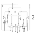
- Fig. 8 illustrates adding a NOR gate to the DFT-enabled FF of Fig. 2 as an alternative method of a generating a "FREEZE_LOW-equivalent" signal.
- Fig. 9 illustrates adding a NOR gate to the DFT-enabled FF of Fig. 6 as an alternative method of a generating a "FREEZE_LOW-equivalent" signal.
- Fig. 10 shows the truth table associated with this implementation - when either or both CC or CR is set to a 1 value, FREEZE_LOW is at a 0 value.
- Fig. 11 shows how adding two inverters and 2 NORs to the DFT-enabled FF (previously shown in Figure 2 ) allows the DFT-enabled FF to behave as a DFT-enabled latch.
- Fig. 12 shows how adding one inverter to the DFT-enabled FF (of Figure 2 ) allows the DFT-enabled FF to behave as a DFT-enabled buffer test point.
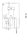
- Figure 13 shows a DFT-enabled latch embodiment that behaves like a flip-flop during scan shift, but behaves like a latch during normal operation and capture mode.
- Figure 14 is the first of two examples of unstable circuits.
- the flip-flop oscillates between 0 to 1 and 1 to 0.
- Figure 15 shows another example of a non-deterministic circuit - in this case, a ring oscillator.
- Figure 16 shows how two DFT-enabled buffers break the loop, without affecting the user circuit's functionality - the user circuit still oscillates.
- Figure 17 shows how one DFT-enabled buffer breaks a loop, without affecting the user circuit's functionality - the user circuit still oscillates.
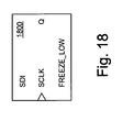
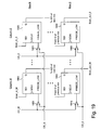
- Figure 18 shows a simplified diagram of a DFT-enabled FF - with the following test pins SDI, SCLK, FREEZE_LOW and the output pin Q is shown.
- Figure 19 shows how the simplified DFT-enabled FFs (of Figure 18 ) can be placed in a two-dimension array and selected using row and column addressing.
- Fig. 20 illustrates a DFT-Enabled FF that eliminates the need for partitioning circuits, simplifies loop breaking, and reduces the vector count required to test circuits.
- Fig. 21 illustrates the timing of the DFT-Enabled FF of Fig. 20 .
- word labels including but not limited to: first, last, certain, various, further, other, particular, select, some, and notable
- word labels may be applied to separate sets of embodiments; as used herein such labels are expressly not meant to convey quality, or any form of preference or prejudice, but merely to conveniently distinguish among the separate sets.
- the order of some operations of disclosed processes is alterable within the scope of the invention.
- multiple embodiments serve to describe variations in process, method, and/or program instruction features
- other embodiments are contemplated that in accordance with a predetermined or a dynamically determined criterion perform static and/or dynamic selection of one of a plurality of modes of operation corresponding respectively to a plurality of the multiple embodiments.
- EC2 The method of EC 1, wherein the DFT-enabled storage circuit is a DFT-enabled flip-flop.
- EC3 The method of EC1, wherein the DFT-enabled storage circuit is a DFT-enabled latch.
- each sequential storage function has normal-operation pins including a clock input and at least one asynchronous control input.
- EC7 The method of EC1, wherein the design-for-testability functionality of the DFT-enabled storage circuit is transparent to the normal operation (i.e., non-test mode operation) of the integrated circuit.
- DFT-enabled FF embodiments are taught herein that insure inherent compliance with the majority of the DFT rules associated with mux-scan. Further embodiments combine the DFT-enabled FF with partition test techniques to achieve testing methods that can test user-designed circuits without requiring any user-inserted test structures - in other words, the test methods are transparent to the user.
- the DFT-enabled FF includes logic that ensures correct scan shift mode, and also provides a novel method of observing (capturing) data.
- Figure 2 shows an implementation of the DFT-enabled FF.
- the user pins are D, CLK, R, S, and Q. From a user's functional viewpoint (e.g., when the DFT-enabled FF is not in test mode), when R has a 1 value, the core flip-flop is asynchronously loaded with a 0 value. From a user's functional viewpoint (e.g., when the DFT-enabled FF is not in test mode), when S has a 1 value, the core flip-flop is asynchronously loaded with a 1 value.
- the core flip-flop has active low asynchronous RN and SN pins, while the DFT-enabled FF implements the user-controlled asynchronous reset R and preset S pins as active high signals, because in current common semiconductor technologies, a 2-input NAND gate usually has a smaller area than a 2-input OR gate of equivalent drive.
- This diagram shows a DFT-enabled FF whose core flip-flop has reset priority, which means the DFT-enabled FF should also implement reset priority.
- the test pins are SDI (scan data in), SCLK (scan clock), SE (scan enable), and FREEZE_LOW (freeze - active low).
- SDI scan data in
- SCLK scan clock
- SE scan enable
- FREEZE_LOW freeze - active low.
- the Q of one DFT-enabled FF is connected to the SDI of the next DFT-enabled FF in the scan chain.
- Some DFT-enabled FF implementations may include a separate SDO (scan data out) pin. In that case, the SDO of one DFT-enabled FF is connected to the SDI of the next DFT-enabled FF in the scan chain.
- This DFT-enabled FF has 3 modes of operation: normal operation mode, scan shift mode, and capture mode.
- a typical scan test sequence is: scan-in, capture mode, and scan-out. Circuit defects are detected when the scan-out values do not match the expected values for a good circuit.
- Figure 3 shows high-level waveforms associated with this DFT-enabled FF's normal operation mode, scan shift mode, and capture mode. (In a scan chain of N-bit depth, there are N SCLK cycles of scan-in and N SCLK cycles of scan-out.)
- the DFT-enabled FF When the DFT-enabled FF's SE pin is at a 1 value, and FREEZE_LOW is at a 0 value, the DFT-enabled FF is in scan shift mode.
- scan shift mode the asynchronous reset RN and asynchronous preset SN pins on the core flip-flop are forced to a 1 value, independent of the values on R and S.
- the user pins, D and CLK, are also bypassed - SCLK is used to clock SDI data into the core flip-flop.
- the DFT-enabled FF ensures that the core flip-flop is not affected by normal operation (user circuit) values. In other words, the core flip-flop is "frozen" with respect to user circuit inputs.
- the DFT-enabled FF is in capture mode when the DFT-enabled FF exits scan shift mode and enters capture mode in order to observe values on the DFT-enabled FF's user pins.
- exiting scan shift mode is known as "unfreeze” or “unfreezing”
- freeze is known as "freeze" or “freezing”.
- Capture mode can observe user circuit values presented on all user pins (D, CLK, S, and R).
- the state of CLK is inferable through manipulation of the SCLK and FREEZE_LOW.
- the DFT-enabled FF's SCLK pin is set to a 0 value and the DFT-enabled FF's CLK pin is a 1 value - a rising edge is automatically generated at the core flip-flop's CLK pin when FREEZE_LOW transitions from a 0 value to a 1 value.
- the SE signal is at a 0 value, the core flip-flop clocks in the value presented at its D input.
- Figure 3 's capture mode waveforms show the rising edge presented to the core flip-flop's CLK pin (MCLK signal).
- the core flip-flop's CLK pin (MCLK signal) will remain a constant 0 value (regardless of the FREEZE_LOW pulse) as shown in Figure 4 .
- the user circuit's values on the R and S pins control the asynchronous reset and preset behavior of the core flip-flop, which enables these functional paths inside the DFT-enabled FF to be verified.
- Figure 6 shows a variation of the DFT-enabled FF.
- the user pins are D, CLK, R, S, and Q. From a user's functional viewpoint (e.g., when the DFT-enabled FF is not in test mode), when R has a 1 value, the core flip-flop is asynchronously loaded with a 0 value. From a user's functional viewpoint (e.g., when the DFT-enabled FF is not in test mode), when S has a 1 value, the core flip-flop is asynchronously loaded with a 1 value.
- This figure shows a DFT-enabled FF whose core flip-flop has preset priority, which means the DFT-enabled FF should also implement preset priority.
- the buffer in the diagram adds sufficient delay to the FREEZE_LOW_delay signal to ensure that if both R and S have a 1 value when the DFT-enabled FF enters capture mode, the core flip-flop will correctly be loaded with a 1 value.
- Figure 7 shows high-level waveforms for capture mode - specifically when both R and S have a 1 value, resulting in the core flip-flop with a final capture value of 1 (preset priority).
- Figure 10 shows the truth table associated with this implementation - when either or both CC or CR is set to a 1 value, FREEZE_LOW is at a 0 value.
- the test pins are SDI (scan data in), SCLK (scan clock), SE (scan enable), and CC (cut column) and CR (cut row).
- Using two signals to place the DFT-enabled FF into freeze mode provides a convenient way of addressing (selecting) a sub-set of DFT-enabled FFs, when the DFT-enabled FFs are arrayed in a regular 2-dimensional array.
- Adding a NOR gate to DFT-enabled simulated latches, DFT-enabled buffers, and DFT-enabled latches also allow them to be mixed with DFT-enabled FFs for arraying in a regular 2-dimensional array.
- the DFT-enabled FF can also implement latch behavior in a user circuit.
- Figure 11 shows how adding two inverters and 2 NORs to the DFT-enabled FF (previously shown in Figure 2 ) allows the DFT-enabled FF to behave as a DFT-enabled latch.
- the user pins are Latch_D, Latch_E, and Q.
- the test pins remain SDI, SCLK, SE, and FREEZE_LOW.
- Latch_E has a 1 value
- the core flip-flop's value depends on the Latch_D value.
- Latch_E has a 0 value
- the core flip-flop holds its current value.
- the DFT-enabled FF can also implement a buffer test point in a user circuit.
- Figure 12 shows how adding one inverter to the DFT-enabled FF (previously shown in Figure 2 ) allows the DFT-enabled FF to behave as a DFT-enabled buffer test point.
- the user pins are TA and TZ.
- the test pins remain SDI, SCLK, SE, and FREEZE_LOW.
- the core flip-flop's value (and TZ pin) is 1.
- the core flip-flop's value (and TZ pin) is 0.
- DFT-enabled buffer test points are useful increasing the testability of a user circuit's without modifying the user circuit's functionality.
- DFT-enabled FF that implements latch behavior (shown in Figure 11 ) will be referred to as a DFT-enabled simulated latch, while the DFT-enabled FF that implements a buffer test point (shown in Figure 12 ) will be referred to as a DFT-enabled buffer.
- Figure 13 shows a DFT-enabled latch embodiment that behaves like a flip-flop during scan shift, but behaves like a latch during normal operation and capture mode.
- the user pins are D, E, and Q.
- the test pins remain SDI, SCLK, SE, and FREEZE_LOW.
- DFT-enabled FFs and DFT-enabled latches can be placed within the same scan chain. If the user pin E is tied high, then the DFT-enabled latch can be used as a DFT-enabled buffer.
- Embodiments are envisioned that consolidate some of the DFT-enabled FF's logic into integrated cells.
- a mux-scan flip-flop or mux flip-flop can be used instead of a discrete mux and flip-flop.
- Other envisioned embodiments consolidate all of the DFT-enabled FF's logic into one integrated cell.
- the DFT-enabled FFs may be implemented with only an asynchronous reset, or with only an asynchronous preset, or without any asynchronous reset or preset. In those cases, the appropriate NAND gate(s) and buffer would not be required and can be removed as an optimization. The muxes shown in Figures 11 and 12 can also be removed as an optimization.
- Embodiments are next described where the DFT-enabled FF, DFT-enabled simulated latch, DFT-enabled buffer, or DFT-enabled latch circuits are combined with addressable control and partition test.
- This testing method can test user circuits without requiring complex DFT rules or any user-inserted test structures.
- This testing method can also test "unstable" circuits; two examples of unstable circuits are shown in Figures 14 and 15 . These circuits are usually considered non-deterministic and untestable from a normal scan test perspective.
- the flip-flop oscillates between 0 to 1 and 1 to 0.
- the flip-flop's user pins are shown because this scenario applies to flip-flops in general. If the flip-flop output has a 0 value, then the asynchronous preset S pin is asserted and the flip-flop is loaded with a 1 value. If the flip-flop output has a 1 value, then the asynchronous reset R pin is asserted and the flip-flop is loaded with a 0 value. A known value can be scanned into the flip-flop. However, the capture (observed) value for this flip-flop is not deterministic because of speed variations caused by manufacturing, temperature and voltage.
- Figure 15 shows another example of a non-deterministic circuit - in this case, a ring oscillator.
- the value of OZ switches from 0 to 1 and 1 to 0.
- the value of OZ at a specific time X after power is applied to the circuit is non-deterministic because the initial conditions at power up cannot be controlled sufficiently. If OZ is driving a flip-flop's user clock pin, then that flip-flop's value at time X also cannot be determined, which means the capture (observed) value for this flip-flop is also non-deterministic.
- loop breaking a concept known as "loop breaking" is introduced.
- component types within a circuit assigned into three different categories: 0_break, 1_break, and 2_break. For counting purposes, 0_breaks are ignored, while two 1_breaks is equivalent to one 2_break.
- DFT-enabled simulated latches ( Figure 11 ), DFT-enabled buffers ( Figure 12 ), and DFT-enabled latches ( Figure 13 ) are 1_break cells.
- DFT-enabled FFs are 1_break cells, when encountered through their user asynchronous preset or reset pins.
- DFT-enabled FFs are 2_break cells, when encountered through their user clock or D pin.
- the entire user circuit is traversed using graph traversal techniques (that are generally known in the art), while keeping track of the number of "breaks" encountered.
- a loop is detected, if a cycle exists (i.e., a node is visited more than once) and the number of breaks is less than two. If the number of breaks is zero, then insert two DFT-enabled buffers to break the loop.
- Figure 16 shows how two DFT-enabled buffers break the loop, without affecting the user circuit's functionality - the user circuit still oscillates. If the number of breaks is one, then insert one DFT-enabled buffer to break the loop.
- Figure 17 shows how one DFT-enabled buffer breaks a loop, without affecting the user circuit's functionality - the user circuit still oscillates. To simplify Figures 16 and 17 only the user pins from each DFT-enabled buffer is shown. Figure 16 also shows only the user pins of the DFT-enabled FF. By inserting DFT-enabled buffers, unstable circuits now have deterministic capture values and are also more testable.
- DFT-enabled FF when the DFT-enabled FF unfreezes, it becomes sensitive to the values on the user pins.
- the DFT-enabled simulated latch, DFT-enabled buffer, and DFT-enabled latch also become sensitive to values on the user pins when they unfreeze.
- DFT-enabled FFs are divided into partitions using the following approach:
- the DFT-enabled FFs within the tested partition can enter capture mode, while the DFT-enabled FFs in all other partitions must remain frozen.
- capture values no longer depend on the order that each DFT-enabled FF unfreezes. In other words, partition test guarantees deterministic capture values.
- Addressable control is a method of that enables DFT-enabled FFs (of the type described herein) to be selected individually, in groups, or in entirety to operate in normal operation mode, scan shift mode, and capture mode.
- the address selection can be pre-designed or can be hard-wired.
- One approach of a pre-designed addressing scheme utilizes row and column addressing, where each DFT-enabled FF is assigned a unique row and column address. Row and column addressing would be efficient in a logic array or gate array. Row and column addressing enables testing of any user-designed circuit that can implemented in the logic array (or gate array); prior knowledge of the user-designed circuits is not required.
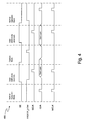
- Figure 18 shows a simplified diagram of a DFT-enabled FF - with the following test pins SDI, SCLK, FREEZE_LOW and the output pin Q is shown.
- the test pin SE and the user pins are not shown.
- Figure 19 shows how the simplified DFT-enabled FFs (of Figure 18 ) can be placed in a two-dimension array and selected using row and column addressing.
- there are M+1 columns (numbered right to left: 0 to M) and there are N+1 rows (numbered bottom to top: 0 to N).
- the DFT-enabled FFs in a column are connected into scan chains.
- Each column has its own column select line (numbered from right to left: CC_0 to CC_M), while each row has its own row select line (numbered from bottom to top: CR_0 to CR_N).
- a row is frozen by setting that row's select line to a 1 value
- a column is frozen by setting that column's select line to a 1 value.
- a DFT-enabled FF is frozen when either or both of its row select line or column select lines is at a 1 value.
- Figures 8 and 9 show two examples of DFT-enabled FFs that are compatible with this row and column addressing method. In this case, each DFT-enabled FF's CC test pin would be connected to the appropriate column select line, and each DFT-enabled FF's CR test pin would be connected to the appropriate row select line.
- DFT-enabled FFs can be addressed (frozen or unfrozen) individually, in groups, or in entirety. When a partition is being tested, only the DFT-enabled FFs in that partition can be selected to enter capture mode.
- DFT-enabled FFs are not arranged in rows and columns - for example, in a standard cell ASIC - hard-wired addressing can be used to select individual, groups or all of the DFT-enabled FFs in the user-designed circuit.
- Hard-wired addressing requires prior knowledge of the user-designed circuit.
- the DFT-enabled FFs in the user-designed circuit are divided into partitions. Each partition requires a separate and distinct FREEZE_LOW signal. All the DFT-enabled FFs in a given partition share the same FREEZE_LOW signal.
- every partition's FREEZE_LOW has a 0 value.
- capture mode only one partition's FREEZE_LOW switches between 0 to 1 to 0 values.
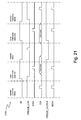
- Fig. 20 illustrates a DFT-Enabled FF 2000 that eliminates the need for partitioning circuits, simplifies loop breaking, and reduces the vector count required to test circuits.
- the Nor gate 935 that is used to generate FREEZE_LOW from CC and CR in the DFT-Enabled FF 900 of Fig. 9 is eliminated, and instead a single freeze_ low signal is brought into the cell 2000.
- the output of flip flop 2025 is run through 2-1 mux 2040 that is controlled by a new signal called freeze_output.
- the other input of the mux 2040 is connected to the output of latch 2030 which has it's D input connected to the output of the new mux 2040 and it's enable input connected to the freeze_output signal.
- Fig. 21 illustrates the timing of the DFT-Enabled FF 2000 of Fig. 20 .
- the freeze output line is held high, and during the Capture mode cycle freeze_output is low and encloses the freeze_low pulse.
- adjacent FFs are partitioned into separate logic cones to insure that testing in a first partition does not inadvertently alter the state of the adjacent FFs.
- the separate partitions are tested in respectively separate test cycles.
- the DFT-Enabled FF 2000 of Fig. 20 allows partitioning to be eliminated because it effectively freezes the driving stimulus to "adjacent" FFs while the FF outputs are captured. Since partitioning is no longer required, individual CC and CR lines are no longer needed to select which partitions are in capture mode. The CC and CR lines are replaced with one freeze_low line. Furthermore, since there are no partitions, every flop can be captured during each test cycle, reducing test vector counts.
- Loop breaking also gets simpler when using the DFT-Enabled FF 2000 of Fig. 20 , because now a flip flop that feeds back to it's own set or reset pin is not a problem and does not need a loop breaking element added. Pure combinational loops must be still broken but they only require a single loop breaking element under all circumstances.
- interconnect and function-unit bit-widths, clock speeds, and the type of technology used are variable according to various embodiments in each component block.
- the names given to interconnect and logic are merely exemplary, and should not be construed as limiting the concepts described.
- the order and arrangement of flowchart and flow diagram process, action, and function elements are variable according to various embodiments.
- value ranges specified, maximum and minimum values used, or other particular specifications are merely those of the described embodiments, are expected to track improvements and changes in implementation technology, and should not be construed as limitations.
Landscapes
- Engineering & Computer Science (AREA)
- General Engineering & Computer Science (AREA)
- Physics & Mathematics (AREA)
- General Physics & Mathematics (AREA)
- Theoretical Computer Science (AREA)
- Computer Hardware Design (AREA)
- Quality & Reliability (AREA)
- Tests Of Electronic Circuits (AREA)
- Semiconductor Integrated Circuits (AREA)
Claims (8)
- Bloc logique (2000) à bascule activée par conception en vue du test, à FF activée par DFT comprenant :une première entrée de commande, une deuxième entrée de commande, une troisième entrée de commande, une entrée de données utilisateur, une entrée de données de balayage, une entrée d'horloge de noyau, une entrée d'horloge de balayage et une sortie ;une première bascule de type D (2025) incluant une première entrée de données, une première sortie de données et une première entrée d'horloge ;un sélecteur d'entrée de données (2010) configuré pour choisir entre l'entrée de données utilisateur et l'entrée de données de balayage en fonction de la première entrée de commande afin de fournir la première entrée de données ; etun sélecteur d'entrée d'horloge (2020) configuré pour choisir entre l'entrée d'horloge de noyau et l'entrée d'horloge de balayage en fonction de la deuxième entrée de commande afin de fournir la première entrée d'horloge ; caractérisé parune seconde bascule de type D (2030) incluant une deuxième entrée de données, une deuxième sortie de données et une troisième sortie couplée à la troisième entrée de données ;un sélecteur de sortie (2040) configuré pour choisir entre la première sortie de données et la deuxième sortie de données en fonction de la troisième entrée de commande afin de fournir une troisième sortie de données couplée à la deuxième entrée de données ;dans lequel la troisième sortie de données fournit la sortie du bloc logique à FF activée par DFT ;dans lequel, dans un mode utilisateur, le sélecteur d'entrée de données (2010) choisit l'entrée de données utilisateur pour un couplage à la première entrée de données et le sélecteur d'entrée d'horloge (2020) choisit l'entrée d'horloge de noyau pour un couplage à la première entrée d'horloge ; etdans lequel, dans un mode de test, le sélecteur d'entrée de données (2010) choisit l'entrée de données de balayage pour un couplage à la première entrée de données et le sélecteur d'entrée d'horloge (2020) choisit l'entrée d'horloge de balayage pour un couplage à la première entrée d'horloge.
- Chaîne de balayage comprenant au moins des premier et second blocs logiques (2000) à FF activée par DFT, chacun selon la revendication 1, dans laquelle la sortie du premier bloc logique (2000) à FF activée par DFT est couplée à l'entrée de données de balayage du second bloc logique (2000) à FF activée par DFT.
- Chaîne de balayage selon la revendication 2, dans laquelle des premières et deuxièmes entrées de commande correspondantes des premier et second blocs logiques (2000) à FF activée par DFT de la chaîne de balayage sont logiquement identiques et sont chacune configurées pour fonctionner dans le mode utilisateur lorsque les premières entrées de commande respectives sont réglées sur les entrées de données utilisateur respectives et que les deuxièmes entrées de données respectives sont réglées sur les entrées d'horloge de noyau respectives.
- Chaîne de balayage selon la revendication 3, dans laquelle les premier et second blocs logiques (2000) à FF activée par DFT de la chaîne de balayage sont configurés pour fonctionner dans un sous-mode de décalage du mode de test lorsque les premières entrées de commande respectives sont réglées sur les entrées de données de balayage respectives et que les deuxièmes entrées de commande respectives sont réglées sur les entrées d'horloge de balayage respectives.
- Chaîne de balayage selon la revendication 3, dans laquelle les premier et second blocs logiques (2000) à FF activée par DFT de la chaîne de balayage sont configurés pour fonctionner dans un sous-mode de saisie du mode de test lorsque les premières entrées de commande respectives sont réglées sur les entrées de données utilisateur respectives et que les troisièmes entrées de commande respectives sont réglées sur les deuxièmes sorties de données respectives ; et
dans laquelle les blocs logiques (2000) à FF activée par DFT sont configurés de telle sorte qu'un résultat de saisie dans le premier bloc logique (2000) à FF activée par DFT n'influence pas le résultat de saisie dans le second bloc logique (2000) à FF activée par DFT. - Chaîne de balayage selon la revendication 5, dans laquelle, dans le sous-mode de saisie, les entrées de données utilisateur respectives sont configurées pour être basculées sélectivement dans la première bascule de type D respective en fonction de l'entrée d'horloge de balayage respective, l'entrée d'horloge de noyau respective, et la deuxième entrée de commande respective.
- Chaîne de balayage selon la revendication 6, dans laquelle la première bascule de type D respective comprend en outre une entrée de réglage asynchrone de noyau respective et une entrée de réinitialisation asynchrone de noyau respective, et dans laquelle les blocs logiques (2000) à FF activée par DFT respectifs comprennent chacun en outre :une logique de porte de réglage (2005) générant un premier signal de commande asynchrone respectif afin d'activer l'entrée de réglage asynchrone de noyau respective lorsqu'une entrée de réglage asynchrone respective et la deuxième entrée de commande respective sont toutes deux dans un état actif ; etune logique de porte de réinitialisation (2015) générant un second signal de commande asynchrone respectif afin d'activer l'entrée de réinitialisation asynchrone de noyau respective lorsqu'une entrée de réinitialisation asynchrone respective et la deuxième entrée de commande respective sont toutes deux dans un état actif ;dans laquelle l'entrée de réglage asynchrone respective et l'entrée de réinitialisation asynchrone respective sont configurées pour être efficaces uniquement dans le mode utilisateur et le sous-mode de saisie.
- Chaîne de balayage selon la revendication 7, dans laquelle les premier et second blocs logiques à FF activée par DFT de la chaîne de balayage comprennent chacun en outre au moins un élément de retard (2030) configuré pour fournir un retard de propagation de front de descente entre les premiers signaux de commande asynchrones respectifs et les seconds signaux de commande asynchrones respectifs si les premiers signaux de commande asynchrones respectifs et les seconds signaux de commande asynchrones respectifs sont activés simultanément.
Applications Claiming Priority (3)
| Application Number | Priority Date | Filing Date | Title |
|---|---|---|---|
| US80428306P | 2006-06-09 | 2006-06-09 | |
| US80508706P | 2006-06-18 | 2006-06-18 | |
| PCT/US2007/070821 WO2007146849A1 (fr) | 2006-06-09 | 2007-06-09 | Procédé de test transparent et bascule à balayage |
Publications (3)
| Publication Number | Publication Date |
|---|---|
| EP2030114A1 EP2030114A1 (fr) | 2009-03-04 |
| EP2030114A4 EP2030114A4 (fr) | 2011-05-18 |
| EP2030114B1 true EP2030114B1 (fr) | 2013-01-23 |
Family
ID=38832108
Family Applications (1)
| Application Number | Title | Priority Date | Filing Date |
|---|---|---|---|
| EP07798355A Active EP2030114B1 (fr) | 2006-06-09 | 2007-06-09 | Procédé de test transparent et bascule à balayage |
Country Status (5)
| Country | Link |
|---|---|
| US (1) | US8122413B2 (fr) |
| EP (1) | EP2030114B1 (fr) |
| JP (1) | JP5131997B2 (fr) |
| KR (1) | KR101006822B1 (fr) |
| WO (1) | WO2007146849A1 (fr) |
Cited By (2)
| Publication number | Priority date | Publication date | Assignee | Title |
|---|---|---|---|---|
| CN109884516A (zh) * | 2019-01-29 | 2019-06-14 | 中国科学院微电子研究所 | 异步复位触发器验证电路以及集成电路验证装置 |
| CN110601811A (zh) * | 2019-09-12 | 2019-12-20 | 北京大学软件与微电子学院 | 一种在dft中使用的安全性的测试模式译码电路 |
Families Citing this family (20)
| Publication number | Priority date | Publication date | Assignee | Title |
|---|---|---|---|---|
| US8332793B2 (en) | 2006-05-18 | 2012-12-11 | Otrsotech, Llc | Methods and systems for placement and routing |
| US8667437B2 (en) * | 2008-03-17 | 2014-03-04 | Xilinx, Inc. | Creating a standard cell circuit design from a programmable logic device circuit design |
| KR20100078431A (ko) * | 2008-12-30 | 2010-07-08 | 주식회사 동부하이텍 | 표준 셀 라이브러리의 성능 개선을 위한 측정 장치 |
| JP5629309B2 (ja) * | 2010-03-15 | 2014-11-19 | 株式会社日立製作所 | 半導体装置およびそのテスト方法 |
| KR101709071B1 (ko) * | 2010-05-19 | 2017-02-22 | 삼성전자주식회사 | 컴프레션 모드 스캔 테스트를 위한 집적 회로 |
| US8788896B2 (en) * | 2012-01-11 | 2014-07-22 | Lsi Corporation | Scan chain lockup latch with data input control responsive to scan enable signal |
| US9086457B2 (en) | 2013-03-26 | 2015-07-21 | International Business Machines Corporation | Scan chain latch design that improves testability of integrated circuits |
| TWI508450B (zh) * | 2013-04-10 | 2015-11-11 | Mstar Semiconductor Inc | 半動態正反器 |
| CN104124946B (zh) * | 2013-04-24 | 2016-10-05 | 晨星半导体股份有限公司 | 半动态触发器 |
| CN104809072A (zh) * | 2013-06-28 | 2015-07-29 | 哈尔滨工业大学 | 基于Perl的EDIF网表级电路的自动可测性设计系统的自动可测性设计方法 |
| US9793881B2 (en) * | 2013-08-05 | 2017-10-17 | Samsung Electronics Co., Ltd. | Flip-flop with zero-delay bypass mux |
| WO2015035144A1 (fr) * | 2013-09-06 | 2015-03-12 | Blue Pearl Software, Inc. | Cellule grise d'utilisateur |
| CN103530479B (zh) * | 2013-10-31 | 2016-09-21 | 哈尔滨工业大学 | 基于Perl的EDIF网表级电路的部分可测性设计系统及部分可测性设计方法 |
| CN103699422A (zh) * | 2013-12-25 | 2014-04-02 | 哈尔滨工业大学 | 使用Perl语言对电路verilog网表描述进行可测性设计的系统及方法 |
| KR101697213B1 (ko) * | 2014-09-02 | 2017-01-17 | 성균관대학교산학협력단 | 디지털 회로의 방사선 내성평가 시스템 및 방사선 내성평가 방법 |
| US10317464B2 (en) * | 2017-05-08 | 2019-06-11 | Xilinx, Inc. | Dynamic scan chain reconfiguration in an integrated circuit |
| US10936774B1 (en) * | 2018-02-15 | 2021-03-02 | Real Intent, Inc. | Methods for identifying integrated circuit failures caused by reset-domain interactions |
| CN110262616B (zh) * | 2019-05-22 | 2021-01-15 | 西安理工大学 | 一种超细粒度控制门级单元电源供应的方法 |
| CN111931445B (zh) * | 2020-10-09 | 2020-12-29 | 芯华章科技股份有限公司 | 用于调试逻辑系统设计的方法、仿真器及存储介质 |
| US11901902B2 (en) | 2021-05-25 | 2024-02-13 | Samsung Electronics Co., Ltd. | Integrated circuit including flip-flop and computing system for designing the integrated circuit |
Family Cites Families (21)
| Publication number | Priority date | Publication date | Assignee | Title |
|---|---|---|---|---|
| JPS63300528A (ja) * | 1987-05-29 | 1988-12-07 | Nec Corp | ゲ−トアレイ集積回路 |
| JP2945103B2 (ja) * | 1990-05-15 | 1999-09-06 | 株式会社リコー | テスト用スキャン回路装置 |
| US5166604A (en) * | 1990-11-13 | 1992-11-24 | Altera Corporation | Methods and apparatus for facilitating scan testing of asynchronous logic circuitry |
| JPH05341016A (ja) * | 1992-06-11 | 1993-12-24 | Seiko Epson Corp | 半導体集積回路装置およびテスト方法 |
| US6096567A (en) * | 1997-12-01 | 2000-08-01 | Electroglas, Inc. | Method and apparatus for direct probe sensing |
| JP3556502B2 (ja) * | 1999-01-20 | 2004-08-18 | 松下電器産業株式会社 | D型フリップフロップ |
| US6393592B1 (en) * | 1999-05-21 | 2002-05-21 | Adaptec, Inc. | Scan flop circuitry and methods for making the same |
| US6701491B1 (en) * | 1999-06-26 | 2004-03-02 | Sei-Yang Yang | Input/output probing apparatus and input/output probing method using the same, and mixed emulation/simulation method based on it |
| JP4428489B2 (ja) | 1999-08-23 | 2010-03-10 | パナソニック株式会社 | 集積回路装置及びそのテスト方法 |
| JP3699019B2 (ja) * | 2001-08-01 | 2005-09-28 | Necマイクロシステム株式会社 | スキャン用フリップフロップおよびスキャンテスト回路 |
| US7127695B2 (en) * | 2002-07-18 | 2006-10-24 | Incentia Design Systems Corp. | Timing based scan chain implementation in an IC design |
| FR2842913B1 (fr) * | 2002-07-23 | 2004-11-19 | Schlumberger Services Petrol | Dispositif compact de mesure de vitesse et de sens de rotation d'un objet |
| US6938225B2 (en) * | 2002-09-04 | 2005-08-30 | Intel Corporation | Scan design for double-edge-triggered flip-flops |
| US7313739B2 (en) * | 2002-12-31 | 2007-12-25 | Analog Devices, Inc. | Method and apparatus for testing embedded cores |
| US7137078B2 (en) | 2003-03-27 | 2006-11-14 | Jasper Design Automation, Inc. | Trace based method for design navigation |
| US20040230933A1 (en) | 2003-05-15 | 2004-11-18 | Weaver Edward G. | Tool flow process for physical design of integrated circuits |
| US7134061B2 (en) * | 2003-09-08 | 2006-11-07 | Texas Instruments Incorporated | At-speed ATPG testing and apparatus for SoC designs having multiple clock domain using a VLCT test platform |
| KR20050051856A (ko) | 2003-11-28 | 2005-06-02 | 삼성전자주식회사 | 디버깅용 주사 체인을 가지는 반도체 장치 및 주사 체인을이용한 디버깅 방법 |
| US7030651B2 (en) * | 2003-12-04 | 2006-04-18 | Viciciv Technology | Programmable structured arrays |
| KR100604904B1 (ko) | 2004-10-02 | 2006-07-28 | 삼성전자주식회사 | 스캔 입력을 갖는 플립 플롭 회로 |
| KR20060066634A (ko) * | 2004-12-13 | 2006-06-16 | 양세양 | 검증 성능과 검증 효율성을 높이는 동적검증 기법 방식의검증 장치 및 이를 이용한 검증 방법론 |
-
2007
- 2007-06-09 EP EP07798355A patent/EP2030114B1/fr active Active
- 2007-06-09 US US12/303,938 patent/US8122413B2/en active Active
- 2007-06-09 WO PCT/US2007/070821 patent/WO2007146849A1/fr active Application Filing
- 2007-06-09 JP JP2009514561A patent/JP5131997B2/ja active Active
- 2007-06-09 KR KR1020097000531A patent/KR101006822B1/ko active IP Right Grant
Cited By (3)
| Publication number | Priority date | Publication date | Assignee | Title |
|---|---|---|---|---|
| CN109884516A (zh) * | 2019-01-29 | 2019-06-14 | 中国科学院微电子研究所 | 异步复位触发器验证电路以及集成电路验证装置 |
| CN109884516B (zh) * | 2019-01-29 | 2021-01-12 | 中国科学院微电子研究所 | 异步复位触发器验证电路以及集成电路验证装置 |
| CN110601811A (zh) * | 2019-09-12 | 2019-12-20 | 北京大学软件与微电子学院 | 一种在dft中使用的安全性的测试模式译码电路 |
Also Published As
| Publication number | Publication date |
|---|---|
| KR101006822B1 (ko) | 2011-01-10 |
| JP2009540302A (ja) | 2009-11-19 |
| EP2030114A1 (fr) | 2009-03-04 |
| US20100169856A1 (en) | 2010-07-01 |
| EP2030114A4 (fr) | 2011-05-18 |
| WO2007146849A1 (fr) | 2007-12-21 |
| KR20090051157A (ko) | 2009-05-21 |
| JP5131997B2 (ja) | 2013-01-30 |
| US8122413B2 (en) | 2012-02-21 |
Similar Documents
| Publication | Publication Date | Title |
|---|---|---|
| EP2030114B1 (fr) | Procédé de test transparent et bascule à balayage | |
| Huang et al. | Testing configurable LUT-based FPGA's | |
| US6021513A (en) | Testable programmable gate array and associated LSSD/deterministic test methodology | |
| Crouch | Design-for-test for Digital IC's and Embedded Core Systems | |
| US6434733B1 (en) | System and method for high-level test planning for layout | |
| US6314539B1 (en) | Boundary-scan register cell with bypass circuit | |
| US6686759B1 (en) | Techniques for testing embedded cores in multi-core integrated circuit designs | |
| Ghosh et al. | Design for hierarchical testability of RTL circuits obtained by behavioral synthesis | |
| JP3842228B2 (ja) | 半導体集積回路装置と設計自動化装置及び方法並びにプログラム | |
| US20020035442A1 (en) | Hierarchical test circuit structure for chips with multiple circuit blocks | |
| JP4361681B2 (ja) | Asic用試験回路 | |
| US7181705B2 (en) | Hierarchical test circuit structure for chips with multiple circuit blocks | |
| WO2001053844A1 (fr) | Structure de circuit de controle hierarchique pour puces a blocs de circuit multiples | |
| US8381050B2 (en) | Method and apparatus for increased effectiveness of delay and transition fault testing | |
| US7111217B1 (en) | Method and system for flexibly nesting JTAG TAP controllers for FPGA-based system-on-chip (SoC) | |
| US6615392B1 (en) | Hierarchical design and test method and system, program product embodying the method and integrated circuit produced thereby | |
| Jahanirad et al. | BIST-based Testing and Diagnosis of LUTs in SRAM-based FPGAs | |
| US7073110B1 (en) | Method and system for programmable boundary-scan instruction register | |
| US4682329A (en) | Test system providing testing sites for logic circuits | |
| US20050015689A1 (en) | Electronic component and method for measuring its qualification | |
| Agrawal et al. | A distributed, reconfigurable, and reusable BIST infrastructure for test and diagnosis of 3-D-Stacked ICs | |
| Aleksejev et al. | Virtual reconfigurable scan-chains on FPGAs for optimized board test | |
| WO2007143220A2 (fr) | Structure de réseau à balayage reconfigurable | |
| Wagner | Robust scan-based logic test in VDSM technologies | |
| Nelson et al. | Physical-design-friendly hierarchical logic built-in self-test—A case study |
Legal Events
| Date | Code | Title | Description |
|---|---|---|---|
| PUAI | Public reference made under article 153(3) epc to a published international application that has entered the european phase |
Free format text: ORIGINAL CODE: 0009012 |
|
| 17P | Request for examination filed |
Effective date: 20090106 |
|
| AK | Designated contracting states |
Kind code of ref document: A1 Designated state(s): AT BE BG CH CY CZ DE DK EE ES FI FR GB GR HU IE IS IT LI LT LU LV MC MT NL PL PT RO SE SI SK TR |
|
| AX | Request for extension of the european patent |
Extension state: AL BA HR MK RS |
|
| DAX | Request for extension of the european patent (deleted) | ||
| RBV | Designated contracting states (corrected) |
Designated state(s): DE FR GB |
|
| RAP1 | Party data changed (applicant data changed or rights of an application transferred) |
Owner name: OTRSOTECH, LIMITED LIABILITY COMPANY |
|
| A4 | Supplementary search report drawn up and despatched |
Effective date: 20110419 |
|
| RIC1 | Information provided on ipc code assigned before grant |
Ipc: G11C 29/00 20060101ALI20110413BHEP Ipc: G01R 31/3185 20060101ALI20110413BHEP Ipc: G06F 11/26 20060101AFI20080228BHEP |
|
| 17Q | First examination report despatched |
Effective date: 20120202 |
|
| REG | Reference to a national code |
Ref country code: DE Ref legal event code: R079 Ref document number: 602007028248 Country of ref document: DE Free format text: PREVIOUS MAIN CLASS: G06F0011260000 Ipc: G11C0029320000 |
|
| RIC1 | Information provided on ipc code assigned before grant |
Ipc: G01R 31/3185 20060101ALI20120613BHEP Ipc: G11C 29/32 20060101AFI20120613BHEP |
|
| GRAP | Despatch of communication of intention to grant a patent |
Free format text: ORIGINAL CODE: EPIDOSNIGR1 |
|
| GRAS | Grant fee paid |
Free format text: ORIGINAL CODE: EPIDOSNIGR3 |
|
| GRAA | (expected) grant |
Free format text: ORIGINAL CODE: 0009210 |
|
| AK | Designated contracting states |
Kind code of ref document: B1 Designated state(s): DE FR GB |
|
| REG | Reference to a national code |
Ref country code: GB Ref legal event code: FG4D |
|
| REG | Reference to a national code |
Ref country code: DE Ref legal event code: R096 Ref document number: 602007028248 Country of ref document: DE Effective date: 20130321 |
|
| PLBE | No opposition filed within time limit |
Free format text: ORIGINAL CODE: 0009261 |
|
| STAA | Information on the status of an ep patent application or granted ep patent |
Free format text: STATUS: NO OPPOSITION FILED WITHIN TIME LIMIT |
|
| 26N | No opposition filed |
Effective date: 20131024 |
|
| REG | Reference to a national code |
Ref country code: DE Ref legal event code: R097 Ref document number: 602007028248 Country of ref document: DE Effective date: 20131024 |
|
| REG | Reference to a national code |
Ref country code: FR Ref legal event code: PLFP Year of fee payment: 9 |
|
| REG | Reference to a national code |
Ref country code: FR Ref legal event code: PLFP Year of fee payment: 10 |
|
| REG | Reference to a national code |
Ref country code: FR Ref legal event code: PLFP Year of fee payment: 11 |
|
| REG | Reference to a national code |
Ref country code: FR Ref legal event code: PLFP Year of fee payment: 12 |
|
| P01 | Opt-out of the competence of the unified patent court (upc) registered |
Effective date: 20230527 |
|
| PGFP | Annual fee paid to national office [announced via postgrant information from national office to epo] |
Ref country code: FR Payment date: 20230509 Year of fee payment: 17 Ref country code: DE Payment date: 20230509 Year of fee payment: 17 |
|
| PGFP | Annual fee paid to national office [announced via postgrant information from national office to epo] |
Ref country code: GB Payment date: 20230510 Year of fee payment: 17 |