EP2023486B1 - Grenzfrequenzregelungsverfahren, GmC-Filterschaltung und Halbleiterbauelement - Google Patents
Grenzfrequenzregelungsverfahren, GmC-Filterschaltung und Halbleiterbauelement Download PDFInfo
- Publication number
- EP2023486B1 EP2023486B1 EP08155300A EP08155300A EP2023486B1 EP 2023486 B1 EP2023486 B1 EP 2023486B1 EP 08155300 A EP08155300 A EP 08155300A EP 08155300 A EP08155300 A EP 08155300A EP 2023486 B1 EP2023486 B1 EP 2023486B1
- Authority
- EP
- European Patent Office
- Prior art keywords
- circuit
- capacitor
- value
- ota
- gmc filter
- Prior art date
- Legal status (The legal status is an assumption and is not a legal conclusion. Google has not performed a legal analysis and makes no representation as to the accuracy of the status listed.)
- Not-in-force
Links
Images



Classifications
-
- H—ELECTRICITY
- H03—ELECTRONIC CIRCUITRY
- H03H—IMPEDANCE NETWORKS, e.g. RESONANT CIRCUITS; RESONATORS
- H03H11/00—Networks using active elements
- H03H11/02—Multiple-port networks
- H03H11/04—Frequency selective two-port networks
- H03H11/0422—Frequency selective two-port networks using transconductance amplifiers, e.g. gmC filters
- H03H11/0472—Current or voltage controlled filters
-
- H—ELECTRICITY
- H03—ELECTRONIC CIRCUITRY
- H03H—IMPEDANCE NETWORKS, e.g. RESONANT CIRCUITS; RESONATORS
- H03H11/00—Networks using active elements
- H03H11/02—Multiple-port networks
- H03H11/04—Frequency selective two-port networks
- H03H11/0422—Frequency selective two-port networks using transconductance amplifiers, e.g. gmC filters
-
- H—ELECTRICITY
- H03—ELECTRONIC CIRCUITRY
- H03H—IMPEDANCE NETWORKS, e.g. RESONANT CIRCUITS; RESONATORS
- H03H11/00—Networks using active elements
- H03H11/02—Multiple-port networks
- H03H11/04—Frequency selective two-port networks
- H03H11/12—Frequency selective two-port networks using amplifiers with feedback
- H03H11/1291—Current or voltage controlled filters
-
- H—ELECTRICITY
- H03—ELECTRONIC CIRCUITRY
- H03H—IMPEDANCE NETWORKS, e.g. RESONANT CIRCUITS; RESONATORS
- H03H2210/00—Indexing scheme relating to details of tunable filters
- H03H2210/02—Variable filter component
- H03H2210/021—Amplifier, e.g. transconductance amplifier
- H03H2210/023—Tuning of transconductance via tail current source
-
- H—ELECTRICITY
- H03—ELECTRONIC CIRCUITRY
- H03H—IMPEDANCE NETWORKS, e.g. RESONANT CIRCUITS; RESONATORS
- H03H2210/00—Indexing scheme relating to details of tunable filters
- H03H2210/04—Filter calibration method
Definitions
- the present invention generally relates to cutoff frequency adjusting methods, GmC filter circuits and semiconductor devices, and more particularly to a cutoff frequency adjusting method for adjusting a cutoff frequency of a GmC filter, a GmC filter circuit which employs such a cutoff frequency adjusting method, and a semiconductor device having such a GmC filter circuit.
- Electronic apparatuses having an analog data processing circuit such as portable telephones, includes a filter circuit for noise reduction and the like.
- a cutoff frequency of the filter circuit deviates depending on inconsistencies that are introduced at a production stage of elements forming the filter circuit, and for this reason, the filter circuit in most cases cannot eliminate all target frequencies.
- FIG. 1 is a circuit diagram showing an example of a conventional GmC filter circuit.
- a GmC filter circuit 1 includes an Operational Transconductance Amplifier (OTA) circuit 2 and a capacitor C that are connected as shown in FIG. 1 .
- Vin an input signal to the GmC filter circuit 1
- Vout an output signal of the GmC filter circuit 1
- C a capacitance of the capacitor C
- Gm a gm value of the OTA circuit 2
- a GmC value of the GmC filter circuit 1 can be set arbitrarily by setting the Gm value of the OTA circuit 2 and the capacitance C of the capacitor C to appropriate designed values.
- the GmC filter circuit 1 has a Low-Pass Filter (LPF) characteristic.
- LPF Low-Pass Filter
- the Gm value and the capacitance C deviate from the respective designed values due to inconsistencies introduced at the production stage of the semiconductor integrated circuit, and the desired LPF characteristic cannot be obtained.
- the cutoff frequency Fc of the GmC filter circuit 1 cannot be determined because there is no means for detecting the GmC value, and it is difficult to form the GmC filter circuit 1 which can maintain the cutoff frequency Fc to a constant value.
- a capacitor having a capacitance equal to or proportional to the capacitance of the capacitor within the GmC filter circuit is provided within the OTA circuit in order to maintain the GmC value constant.
- a switched capacitor may be used for the capacitor within the OTA circuit, and the GmC value can be controlled constant by constantly inputting an arbitrary clock to the GmC filter circuit.
- the clock must constantly be input to the GmC filter circuit, and it is difficult to reduce the power consumption of the GmC filter circuit. For this reason, this kind of GmC filter circuit is unsuited for use in electronic apparatuses which require low power consumption, such as portable telephones.
- a filter circuit using a conductance amplifier is proposed in a Japanese Laid-Open Patent Application No. 2004-266316 .
- GmC filter circuits are proposed in Japanese Laid-Open Patent Applications No. 2003-8398 , No. 2005-348109 and No. 2005-286778 , for example.
- the Japanese Laid-Open Patent Application No. 2005-348109 proposes a GmC filter circuit using a switched capacitor.
- Another and more specific object of the present invention is to provide a cutoff frequency adjusting method, a GmC filter circuit and a semiconductor device, which can simultaneously maintain the GmC value constant and realize a low power consumption.
- a cutoff frequency adjusting method for adjusting a cutoff frequency of a GmC filter circuit which has a capacitor and an Operational Transconductance Amplifier (OTA) circuit with a controllable Gm value, characterized in that there are provided the steps of (a) detecting a Gm value of the OTA circuit based on a voltage of the capacitor which is charged by an output of the OTA circuit; and (b) setting a cutoff frequency of the GmC circuit to a desired value by controlling the Gm value of the OTA circuit constant based on the Gm value detected in said step (a).
- the cutoff frequency adjusting method it is possible to simultaneously maintain the GmC value constant and realize a low power consumption.
- a GmC filter circuit characterized in that there are provided an Operational Transconductance Amplifier (OTA) circuit with a controllable Gm value; a capacitor; a detecting circuit configured to detect a Gm value based on a voltage of the capacitor which is charged by an output of the OTA circuit; and a control circuit configured to set a cutoff frequency of the GmC filter circuit to a desired value by controlling the Gm value of the OTA circuit constant based on the Gm value detected by the detecting circuit.
- OTA Operational Transconductance Amplifier
- a semiconductor device characterized in that there is provided a GmC filter circuit, wherein the GmC filter circuit comprises an Operational Transconductance Amplifier (OTA) circuit with a controllable Gm value; a capacitor; a detecting circuit configured to detect a Gm value based on a voltage of the capacitor which is charged by an output of the OTA circuit; and a control circuit configured to set a cutoff frequency of the GmC filter circuit to a desired value by controlling the Gm value of the OTA circuit constant based on the Gm value detected by the detecting circuit.
- OTA Operational Transconductance Amplifier
- a cutoff frequency of a GmC filter circuit which has a capacitor and an Operational Transconductance Amplifier (OTA) circuit with a controllable Gm value, is automatically adjusted.
- a Gm value of the OTA circuit is detected based on a voltage of the capacitor which is charged by an output of the OTA circuit, and a cutoff frequency of the GmC circuit is set to a desired value by controlling the Gm value of the OTA circuit constant based on the detected Gm value.
- OTA Operational Transconductance Amplifier
- FIG. 2 is a circuit diagram showing a GmC filter circuit in a first embodiment of the present invention.
- a GmC filter circuit 11 includes an OTA circuit 12 having a controllable gm value, switches SW1, SW2 and SW3, a capacitor C, a comparator circuit 13 and a control circuit 14 which are connected as shown in FIG. 2 .
- the switches SW1, SW2 and SW3 and the capacitor C are connected via a node N1.
- a capacitance of the capacitor C is denoted by C
- the gm value of the OTA circuit 12 is denoted by Gm
- Vref a reference signal input to the comparator circuit 13
- An input signal Vin to the GmC filter circuit 11 is input to the OTA circuit 12, and an input signal Vin having a known value Vinref is input to the OTA circuit 12 when adjusting the Gm value of the OTA circuit 12.
- An output signal Vout of the GmC filter circuit 11 is output via the node N1.
- An output signal Vcomp of the comparator circuit 13 is fed back to the OTA circuit 12 via the control circuit 14, and the Gm value of the OTA circuit 12 is controlled by a bias control of a control signal VB which is output from the control circuit 14.
- ON and OFF timings (hereinafter simply referring to as ON/OFF timings) of the switches SW1, SW2 and SW3 may be controlled by ON/OFF control signals output from the control circuit 14 within the GmC filter circuit 11 or, by ON/OFF control signals output from a control means (not shown), such as a control circuit, a controller and a processor, such as a Central Processing Unit (CPU), which is provided outside the GmC filter circuit 11.
- a control means such as a control circuit, a controller and a processor, such as a Central Processing Unit (CPU), which is provided outside the GmC filter circuit 11.
- CPU Central Processing Unit
- the cutoff frequency adjusting method adjusts a cutoff frequency Fc of the GmC filter circuit 11 by feeding back the output signal Vcomp of the comparator circuit 13 to the OTA circuit 12, and controlling the Gm value of the OTA circuit 12 by controlling the ON/OFF timings of the switches SW1, SW2 and SW3 by the control circuit or means which is internal or external to the GmC filter circuit 11, in order to control the Gm value of the OTA circuit 12.
- the ON/OFF timings of the switches SW1, SW2 and SW3 are controlled by the control means which is external to the GmC filter circuit 11, the output signal Vcomp of the comparator circuit 13 is supplied to this external control means.
- the GmC filter circuit 11 When forming the GmC filter circuit 11 in a semiconductor integrated circuit such as a Large Scale Integrated (LSI) circuit, the GmC filter circuit 11 is formed on the same substrate as the external control means (that is, the control circuit, the controller or the processor, such as the CPU), which is provided externally to the GmC filter circuit 11, to thereby form a semiconductor device or semiconductor chip.
- the external control means that is, the control circuit, the controller or the processor, such as the CPU
- LPF Low-Pass Filter
- the GmC value of the GmC filter circuit 11 can be set arbitrarily by setting the Gm value of the OTA circuit 12 and the capacitance C of the capacitor C to appropriate designed values.
- the Gm value and the capacitance C deviate from the respective designed values due to inconsistencies introduced during the production stage of the semiconductor integrated circuit.
- the Gm value of the OTA circuit 12 is controlled based on the output signal Vcomp of the comparator circuit 13 in order to control the Gm/C value constant and to maintain the LPF characteristic constant.
- FIG. 3 is a circuit diagram showing the OTA circuit 12.
- the OTA circuit 12 includes current sources 121 and 122, and NMOS transistors 123, 124 and 125 which are connected as shown in FIG. 3 .
- the input signal Vin is input to a gate of the NMOS transistor 123
- the control signal VB is input to a gate of the NMOS transistor 125.
- V DD denotes a power supply voltage
- SG denotes a reference signal input to a gate of the NMOS transistor 124
- I SS denotes a tail current flowing through the NMOS transistor 125
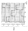
- FIG. 4 is a time chart for explaining an operation of the GmC filter circuit 11.
- the ordinate indicates the voltage (V)
- the abscissa indicates the time ( ⁇ s).
- FIG. 4 (a) shows the output signal Vcomp of the comparator circuit 13
- (b) shows the ON/OFF control signal input to the switch SW3
- (c) shows the ON/OFF control signal input to the switch SW1
- (d) shows the ON/OFF control signal input to the switch SW2
- e shows a potential at the node N1, that is, the output signal Vout of the GmC filter circuit 11.
- each of the switches SW1, SW2 and SW3 is turned ON (that is, assumes a closed state for passing an incoming signal) during a high-level period of the ON/OFF control signal that is input thereto, and is turned OFF (that is, assumes an open state for blocking an incoming signal) during a low-level period of the ON/OFF control signal that is input thereto.
- the switch SW3 is turned ON for a time t1 to carry out an initializing (or clearing) process in order to discharge the charge in the capacitor C1, and the switch SW3 is thereafter turned OFF for a time t2 in order to enable a charge to be charged in the capacitor C.
- the input signal Vin to the GmC filter circuit 11 is input to the OTA circuit 12, and the switch SW1 is turned ON for a time t3 as shown in FIG. 4(c) .
- Vc (Vin ⁇ Gm)t3/C.
- the switch SW1 is turned OFF, and the switch SW2 is turned ON for a time t4 as shown in FIG. 4(d) .
- a relationship t2 > (t3 + t4) stands among the times t2, t3 and t4.
- the value of the reference signal Vref is preset to the value of the voltage Vc which is required to obtain a desired GmC value.
- the switches SW1, SW2 and SW3 and the comparator circuit 13 form a detecting circuit or means for detecting the Gm value of the OTA circuit 12.
- the control circuit 14 judges that the Gm value of the OTA circuit 12 is the designed value when the output signal Vcomp of the comparator circuit 13 has a high level in the case of the positive logic, and when the output signal Vcomp of the comparator circuit 13 has a low level in the case of the negative logic.
- the control circuit 14 judges that the Gm value of the OTA circuit 12 is the designed value, the control circuit 14 supplies the control signal VB, corresponding to the designed Gm value, to the OTA circuit 12 of the GmC filter circuit 11.
- the comparator circuit 13 compares the voltage Vc and the voltage of the reference signal Vref, and turns the switch SW2 OFF and turns the switch SW3 ON when Vc ⁇ Vref, in order to short-circuit the two terminals of the capacitor C and clear (or discharge) the charge.
- the LPF characteristic can be maintained constant by controlling the Gm/C value constant, by controlling the Gm value of the OTA circuit 12 based on the output signal Vcomp of the comparator circuit 13.
- the cutoff frequency Fc of the GmC filter circuit 11 it is possible to set the cutoff frequency Fc of the GmC filter circuit 11 to a desired value.
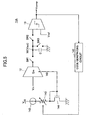
- FIG. 5 is a circuit diagram showing a GmC filter circuit in a second embodiment of the present invention.
- a GmC filter circuit 11A includes, in a feedback path of the output signal Vcomp of the comparator circuit 13, a code generating circuit 141, a current source 142, a variable resistor 143 and an NMOS transistor 144 which are connected as shown in FIG. 5 .
- the code generating circuit 141, the current source 142, the variable resistor 143 and the NMOS transistor 144 correspond to the control circuit 14 of the first embodiment shown in FIG. 2 .
- the code generating circuit 141 maintains the value of an output code when the output signal Vcomp of the comparator circuit 13 has a high level, and increases the value of the output code by a predetermined value when the output signal Vcomp of the comparator circuit 13 has a low level. For example, the value of the output code when the output signal Vcomp of the comparator circuit 13 has the high level is held in a register (not shown) within the code generating circuit 141.
- a resistance of the variable resistor 143 which is connected to the current source 142 is variable set based on the output code from the code generating circuit 141, and the resistance of the variable resistor 143 increases when the value of the output code increases.
- the control signal VB which is supplied to the OTA circuit 12 is output from a gate of the NMOS transistor 144 which has the gate and a source that are connected in common to the variable resistor 143 and has a drain that is grounded.
- FIG. 6 is a circuit diagram showing a GmC filter circuit in a third embodiment of the present invention.
- those parts that are the same as those corresponding parts in FIG. 2 are designated by the same reference numerals, and a description thereof will be omitted.
- a plurality of GmC filter circuits having the same basic structure are provided within a single semiconductor device.
- a control circuit for controlling the Gm value may only be provided with respect to one GmC filter circuit in order to simplify the circuit structure.
- the control signal VB which is output from the control circuit is supplied to each of the GmC filter circuits within the single semiconductor device.
- a first GmC filter circuit 11 of the first embodiment having the structure shown in FIG. 2 or, a first GmC filter circuit 11A of the second embodiment having the structure shown in FIG. 5 , and one or a plurality of second GmC filter circuits 52 are provided within a single semiconductor device 51 as shown in FIG. 6 .
- Each second GmC filter circuit 52 has the same basic structure as the first GmC filter circuit 11, and is made up solely of an OTA circuit 12 and a capacitor C which are produced by the same production processes as the OTA circuit 12 and the capacitor C within the GmC filter circuit 11.
- each second GmC filter circuit 52 has the same basic structure as the first GmC filter circuit 11A, and is made up solely of an OTA circuit 12 and a capacitor C which are produced by the same production processes as the OTA circuit 12 and the capacitor C within the GmC filter circuit 11A.
- the control signal VB generated within the first GmC filter circuit 11 or 11A is supplied to the OTA circuit 12 within the first GmC filter circuit 11 or 11A and to the OTA circuit 12 within each second GmC filter circuit 52.
- the Gm/C values of all of the first GmC filter circuit 11 or 11A and the one or plurality of second GmC filter circuits 52 are maintained constant and the respective cutoff frequencies Fc are set to desired values.
- the first and second GmC filter circuits 11 or 11A and 52 have the same basic structure, and the OTA circuits 12 and the capacitors C of the first and second GmC filter circuits 11 or 11A and 52 are produced by the same production processes. In other words, the inconsistencies in the OTA circuits 12 and the capacitors C introduced at the production stage are the same for each of the first and second GmC filter circuits 11 or 11A and 52.
- Vin1 and Vin2 denote input signals of corresponding second GmC filter circuits 52
- Vout1 and Vout2 denote output signals of the corresponding second GmC filter circuits 52.
Landscapes
- Networks Using Active Elements (AREA)
Claims (7)
- GmC-Filterschaltung (11A), in der vorgesehen sind:eine Transkonduktanz-Operationsverstärker-(OTA)-Schaltung (12) mit steuerbarem Gm-Wert;ein Kondensator (C);eine Detektionsschaltung, die konfiguriert ist, um einen Gm-Wert auf der Basis einer Spannung des Kondensators (Vc) zu detektieren, der durch eine Ausgabe der OTA-Schaltung (12) geladen wird; undeine Steuerschaltung (14), die konfiguriert ist, um eine Grenzfrequenz der GmC-Filterschaltung durch Konstantsteuerung des Gm-Wertes der OTA-Schaltung auf der Basis des durch die Detektionsschaltung detektierten Gm-Wertes auf einen gewünschten Wert zu setzen, dadurch gekennzeichet, dassdie Steuerschaltung (14) eine Codeerzeugungsschaltung (141) mit einem Register, eine Stromquelle (142), einen veränderbare Widerstand (143) und einen NMOS-Transistor (144) enthält.
- GmC-Filterschaltung (11A) nach Anspruch 1, bei der die Detektionsschaltung umfasst:einen ersten Schalter (SW1), der konfiguriert ist, um den Kondensator (C) zu laden, indem die Ausgabe der OTA-Schaltung (12) dem Kondensator (C) während einer bekannten Zeit zugeführt wird; undeine Komparatorschaltung (13), die konfiguriert ist, um die Spannung des Kondensators (Vc), der geladen ist, und eine Spannung des Kondensator (Vref) zu vergleichen, wenn der Gm-Wert erhalten wird, der einen gewünschten Wert hat;bei der die Steuerschaltung (14) eine Rückführungssteuerung ausführt, wodurch der Gm-Wert der OTA-Schaltung (12) erhöht wird, wenn die Komparatorschaltung (13) ein Signal ausgibt, das angibt, dass die Spannung des Kondensators (Vc), der geladen ist, niedriger als die Spannung des Kondensators (Vref) ist, wenn der Gm-Wert den gewünschten Wert hat.
- GmC-Filterschaltung (11A) nach Anspruch 2, in der ferner vorgesehen ist:ein zweiter Schalter (SW3), der konfiguriert ist, um einen Initialisierungsprozess durch Kurzschließen des Kondensators (C) vor dem Detektieren des Gm-Wertes durch die Detektionsschaltung auszuführen.
- GmC-Filterschaltung (11A) nach Anspruch 3, in der ferner vorgesehen ist:ein dritter Schalter (SW2), der konfiguriert ist, um die Spannung des Kondensators (Vc), der geladen ist, der Komparatorschaltung (13) zuzuführen.
- GmC-Filterschaltung (11A) nach Anspruch 3, bei der die Steuerschaltung (14) eine Zeitlage steuert, wenn der Kondensator (C) durch den zweiten Schalter (SW3) kurzgeschlossen wird, eine Zeitlage, wenn der Kondensator (C) durch Zuführen der Ausgabe der OTA-Schaltung (12) zu dem Kondensator (C) während der bekannten Zeit durch den ersten Schalter (SW1) geladen wird, und eine Zeitlage, wenn der dritte Schalter (SW2) die Spannung des Kondensators (Vc), der geladen ist, der Komparaturschaltung (13) zuführt und die Komparatorschaltung die Spannung des Kondensators (Vc), der geladen ist, und die Spannung des Kondensators (Vref) vergleicht, wenn der Gm-Wert, der den gewünschten Wert hat, erhalten wird.
- Halbleiterbauelement (51), in dem vorgesehen ist:die GmC-Filterschaltung (11A) nach Anspruch 1.
- Halbleiterbauelement (51) nach Anspruch 6, in dem ferner vorgesehen ist:eine oder eine Vielzahl von GmC-Filterschaltungen (52), die jeweils eine OTA-Schaltung (12) haben, die mit der genannten OTA-Schaltung (12) identisch ist, und einen Kondensator (C), der mit dem genannten Kondensator (C) identisch ist,bei dem ein Steuersignal (VB) zur Konstantsteuerung des Gm-Wertes der OTA-Schaltung der genannten OTA-Schaltung (12) und jeder OTA-Schaltung (12) der genannten einen oder der Vielzahl von GmC-Filterschaltungen (52) zugeführt wird.
Applications Claiming Priority (1)
| Application Number | Priority Date | Filing Date | Title |
|---|---|---|---|
| JP2007193424A JP2009033323A (ja) | 2007-07-25 | 2007-07-25 | カットオフ周波数調整方法、GmCフィルタ回路及び半導体装置 |
Publications (2)
| Publication Number | Publication Date |
|---|---|
| EP2023486A1 EP2023486A1 (de) | 2009-02-11 |
| EP2023486B1 true EP2023486B1 (de) | 2010-08-04 |
Family
ID=39639435
Family Applications (1)
| Application Number | Title | Priority Date | Filing Date |
|---|---|---|---|
| EP08155300A Not-in-force EP2023486B1 (de) | 2007-07-25 | 2008-04-28 | Grenzfrequenzregelungsverfahren, GmC-Filterschaltung und Halbleiterbauelement |
Country Status (4)
| Country | Link |
|---|---|
| US (1) | US7764116B2 (de) |
| EP (1) | EP2023486B1 (de) |
| JP (1) | JP2009033323A (de) |
| DE (1) | DE602008002021D1 (de) |
Families Citing this family (9)
| Publication number | Priority date | Publication date | Assignee | Title |
|---|---|---|---|---|
| US7782127B2 (en) * | 2008-01-25 | 2010-08-24 | Broadcom Corporation | Multi-mode reconstruction filter |
| US9059773B2 (en) * | 2009-10-11 | 2015-06-16 | SiTune Corporation | Radio frequency tuner |
| JP5423875B2 (ja) * | 2010-03-23 | 2014-02-19 | 富士通株式会社 | 周波数可変フィルタ |
| JP5667503B2 (ja) * | 2011-04-13 | 2015-02-12 | 三菱電機株式会社 | フィルタ装置 |
| JP6132655B2 (ja) * | 2013-05-13 | 2017-05-24 | オリンパス株式会社 | 信号処理回路およびカプセル内視鏡 |
| US10181840B1 (en) | 2014-08-21 | 2019-01-15 | National Technology & Engineering Solutions Of Sandia, Llc | Gm-C filter and multi-phase clock circuit |
| KR101832733B1 (ko) * | 2016-08-10 | 2018-02-28 | 지투지솔루션(주) | 생체 신호 측정 시스템 |
| KR101832734B1 (ko) * | 2016-08-10 | 2018-02-28 | 지투지솔루션(주) | 개선된 생체 신호 측정 시스템 |
| CN121036752A (zh) * | 2025-08-13 | 2025-11-28 | 北京石油化工学院 | 一种带滤波功能的接口电路 |
Family Cites Families (16)
| Publication number | Priority date | Publication date | Assignee | Title |
|---|---|---|---|---|
| JP2973491B2 (ja) * | 1990-08-22 | 1999-11-08 | ソニー株式会社 | Ntsc/pal信号判別回路およびこの判別回路を用いたアクティブフィルタ |
| JP2829123B2 (ja) * | 1990-11-15 | 1998-11-25 | 株式会社東芝 | 自動調整icフィルタ回路 |
| JP3318725B2 (ja) * | 1994-01-12 | 2002-08-26 | 株式会社日立製作所 | アナログフィルタ回路 |
| US6112125A (en) * | 1995-03-08 | 2000-08-29 | Silicon Systems, Inc. | Self-tuning method and apparatus for continuous-time filters |
| JPH08298438A (ja) * | 1995-04-26 | 1996-11-12 | Hitachi Ltd | 半導体集積回路装置 |
| US6084465A (en) * | 1998-05-04 | 2000-07-04 | Tritech Microelectronics, Ltd. | Method for time constant tuning of gm-C filters |
| US6304135B1 (en) * | 1999-11-17 | 2001-10-16 | Texas Instruments Incorporated | Tuning method for Gm/C filters with minimal area overhead and zero operational current penalty |
| JP2003008398A (ja) | 2001-06-25 | 2003-01-10 | Matsushita Electric Ind Co Ltd | フィルタ回路 |
| JP4566742B2 (ja) * | 2002-09-05 | 2010-10-20 | エヌエックスピー ビー ヴィ | 連続時間フィルタの自己キャリブレーション、およびかかるフィルタを備えるシステム |
| JP4045959B2 (ja) | 2003-01-20 | 2008-02-13 | 日本電気株式会社 | 利得可変電圧・電流変換回路とこれを用いたフィルタ回路 |
| EP1513253A1 (de) * | 2003-09-05 | 2005-03-09 | Semiconductor Ideas to The Market (ItoM) BV | Programmierbarer Hochpräzisionsfilter |
| JP2005286778A (ja) | 2004-03-30 | 2005-10-13 | Toyota Industries Corp | フィルタ |
| JP2005348109A (ja) | 2004-06-03 | 2005-12-15 | Toyota Industries Corp | gmCフィルタの周波数自動調整回路、相互コンダクタンス増幅器のgm自動調整回路及びそのMOS集積回路 |
| TWI312231B (en) * | 2005-02-17 | 2009-07-11 | Via Tech Inc | Gm-c time constant tuning circuit |
| KR100633361B1 (ko) * | 2005-05-12 | 2006-10-13 | 인티그런트 테크놀로지즈(주) | 튜닝 회로. |
| KR100750650B1 (ko) * | 2005-06-22 | 2007-08-20 | 인티그런트 테크놀로지즈(주) | 튜닝 회로. |
-
2007
- 2007-07-25 JP JP2007193424A patent/JP2009033323A/ja active Pending
-
2008
- 2008-04-28 EP EP08155300A patent/EP2023486B1/de not_active Not-in-force
- 2008-04-28 DE DE602008002021T patent/DE602008002021D1/de active Active
- 2008-04-29 US US12/111,556 patent/US7764116B2/en active Active
Also Published As
| Publication number | Publication date |
|---|---|
| EP2023486A1 (de) | 2009-02-11 |
| DE602008002021D1 (de) | 2010-09-16 |
| US7764116B2 (en) | 2010-07-27 |
| JP2009033323A (ja) | 2009-02-12 |
| US20090027115A1 (en) | 2009-01-29 |
Similar Documents
| Publication | Publication Date | Title |
|---|---|---|
| US7764116B2 (en) | Cutoff frequency adjusting method, GmC filter circuit and semiconductor device | |
| US9014398B2 (en) | Charging circuit and amplifier | |
| US8111093B2 (en) | Power supply noise rejection in PLL or DLL circuits | |
| US7929716B2 (en) | Voltage supply circuit, power supply circuit, microphone unit using the same, and microphone unit sensitivity adjustment method | |
| US7724551B2 (en) | Step-up circuit and portable device using it | |
| US12323062B2 (en) | Multi-phase switching regulator including interleaving circuit and switching regulating method using the same | |
| JP5676961B2 (ja) | 電源の制御回路、電子機器及び電源の制御方法 | |
| US20110156760A1 (en) | Temperature-stable oscillator circuit having frequency-to-current feedback | |
| US9444468B2 (en) | Oscillator devices and methods | |
| US8008978B2 (en) | Oscillator circuit and memory system | |
| KR101725862B1 (ko) | 스위칭 레귤레이터, 이의 동작 방법, 및 이를 포함하는 전자 장치 | |
| US20080007443A1 (en) | Input interface circuit adapted to both of analog and digital signals | |
| CN116643609B (zh) | 具有电源噪声消除的电压调节器 | |
| CN100587646C (zh) | 电压供应电路、电源电路、扩音器单元及灵敏度调节方法 | |
| US7026824B2 (en) | Voltage reference generator with negative feedback | |
| JP2007281876A (ja) | 比較回路及びその増幅回路 | |
| JPH08223018A (ja) | ばらつき補償技術による半導体集積回路 | |
| US8373500B2 (en) | Voltage biasing circuit and data processing system having the same | |
| KR20150019000A (ko) | 기준 전류 생성 회로 및 이의 구동 방법 | |
| USRE40053E1 (en) | Delay circuit having delay time adjustable by current | |
| US8058923B2 (en) | Charge pump circuit and slice level control circuit | |
| US7064599B1 (en) | Apparatus and method for signal transmission | |
| WO2015072679A1 (en) | Device and method for controlling output amplitude of voltage control oscillator in electronic device | |
| CN110869874B (zh) | 升压产生电路以及相关电路、芯片以及穿戴设备 | |
| JP2008507023A (ja) | バッテリ給電ハンドセット装置用のコモンモード電圧発生器 |
Legal Events
| Date | Code | Title | Description |
|---|---|---|---|
| PUAI | Public reference made under article 153(3) epc to a published international application that has entered the european phase |
Free format text: ORIGINAL CODE: 0009012 |
|
| AK | Designated contracting states |
Kind code of ref document: A1 Designated state(s): AT BE BG CH CY CZ DE DK EE ES FI FR GB GR HR HU IE IS IT LI LT LU LV MC MT NL NO PL PT RO SE SI SK TR |
|
| AX | Request for extension of the european patent |
Extension state: AL BA MK RS |
|
| 17P | Request for examination filed |
Effective date: 20090805 |
|
| AKX | Designation fees paid |
Designated state(s): DE FR GB |
|
| GRAP | Despatch of communication of intention to grant a patent |
Free format text: ORIGINAL CODE: EPIDOSNIGR1 |
|
| RAP1 | Party data changed (applicant data changed or rights of an application transferred) |
Owner name: FUJITSU SEMICONDUCTOR LIMITED |
|
| GRAS | Grant fee paid |
Free format text: ORIGINAL CODE: EPIDOSNIGR3 |
|
| GRAA | (expected) grant |
Free format text: ORIGINAL CODE: 0009210 |
|
| AK | Designated contracting states |
Kind code of ref document: B1 Designated state(s): DE FR GB |
|
| REG | Reference to a national code |
Ref country code: GB Ref legal event code: FG4D |
|
| REF | Corresponds to: |
Ref document number: 602008002021 Country of ref document: DE Date of ref document: 20100916 Kind code of ref document: P |
|
| PLBE | No opposition filed within time limit |
Free format text: ORIGINAL CODE: 0009261 |
|
| STAA | Information on the status of an ep patent application or granted ep patent |
Free format text: STATUS: NO OPPOSITION FILED WITHIN TIME LIMIT |
|
| 26N | No opposition filed |
Effective date: 20110506 |
|
| REG | Reference to a national code |
Ref country code: DE Ref legal event code: R097 Ref document number: 602008002021 Country of ref document: DE Effective date: 20110506 |
|
| REG | Reference to a national code |
Ref country code: FR Ref legal event code: ST Effective date: 20111230 |
|
| PG25 | Lapsed in a contracting state [announced via postgrant information from national office to epo] |
Ref country code: FR Free format text: LAPSE BECAUSE OF NON-PAYMENT OF DUE FEES Effective date: 20110502 |
|
| GBPC | Gb: european patent ceased through non-payment of renewal fee |
Effective date: 20120428 |
|
| PG25 | Lapsed in a contracting state [announced via postgrant information from national office to epo] |
Ref country code: GB Free format text: LAPSE BECAUSE OF NON-PAYMENT OF DUE FEES Effective date: 20120428 |
|
| REG | Reference to a national code |
Ref country code: DE Ref legal event code: R082 Ref document number: 602008002021 Country of ref document: DE Representative=s name: REICHERT & LINDNER PARTNERSCHAFT PATENTANWAELT, DE |
|
| REG | Reference to a national code |
Ref country code: DE Ref legal event code: R082 Ref document number: 602008002021 Country of ref document: DE Representative=s name: REICHERT & LINDNER PARTNERSCHAFT PATENTANWAELT, DE Effective date: 20150512 Ref country code: DE Ref legal event code: R081 Ref document number: 602008002021 Country of ref document: DE Owner name: SOCIONEXT INC., YOKOHAMA-SHI, JP Free format text: FORMER OWNER: FUJITSU SEMICONDUCTOR LTD., YOKOHAMA, KANAGAWA, JP Effective date: 20150512 |
|
| PGFP | Annual fee paid to national office [announced via postgrant information from national office to epo] |
Ref country code: DE Payment date: 20240418 Year of fee payment: 17 |
|
| REG | Reference to a national code |
Ref country code: DE Ref legal event code: R119 Ref document number: 602008002021 Country of ref document: DE |
|
| PG25 | Lapsed in a contracting state [announced via postgrant information from national office to epo] |
Ref country code: DE Free format text: LAPSE BECAUSE OF NON-PAYMENT OF DUE FEES Effective date: 20251104 |