EP2023331A1 - Anzeigevorrichtung und Verfahren zu ihrer Ansteuerung - Google Patents
Anzeigevorrichtung und Verfahren zu ihrer Ansteuerung Download PDFInfo
- Publication number
- EP2023331A1 EP2023331A1 EP08006206A EP08006206A EP2023331A1 EP 2023331 A1 EP2023331 A1 EP 2023331A1 EP 08006206 A EP08006206 A EP 08006206A EP 08006206 A EP08006206 A EP 08006206A EP 2023331 A1 EP2023331 A1 EP 2023331A1
- Authority
- EP
- European Patent Office
- Prior art keywords
- gate
- pixel
- signal
- sub
- clock signal
- Prior art date
- Legal status (The legal status is an assumption and is not a legal conclusion. Google has not performed a legal analysis and makes no representation as to the accuracy of the status listed.)
- Pending
Links
Images

Classifications
-
- G—PHYSICS
- G09—EDUCATION; CRYPTOGRAPHY; DISPLAY; ADVERTISING; SEALS
- G09G—ARRANGEMENTS OR CIRCUITS FOR CONTROL OF INDICATING DEVICES USING STATIC MEANS TO PRESENT VARIABLE INFORMATION
- G09G3/00—Control arrangements or circuits, of interest only in connection with visual indicators other than cathode-ray tubes
- G09G3/20—Control arrangements or circuits, of interest only in connection with visual indicators other than cathode-ray tubes for presentation of an assembly of a number of characters, e.g. a page, by composing the assembly by combination of individual elements arranged in a matrix no fixed position being assigned to or needed to be assigned to the individual characters or partial characters
- G09G3/34—Control arrangements or circuits, of interest only in connection with visual indicators other than cathode-ray tubes for presentation of an assembly of a number of characters, e.g. a page, by composing the assembly by combination of individual elements arranged in a matrix no fixed position being assigned to or needed to be assigned to the individual characters or partial characters by control of light from an independent source
- G09G3/36—Control arrangements or circuits, of interest only in connection with visual indicators other than cathode-ray tubes for presentation of an assembly of a number of characters, e.g. a page, by composing the assembly by combination of individual elements arranged in a matrix no fixed position being assigned to or needed to be assigned to the individual characters or partial characters by control of light from an independent source using liquid crystals
- G09G3/3607—Control arrangements or circuits, of interest only in connection with visual indicators other than cathode-ray tubes for presentation of an assembly of a number of characters, e.g. a page, by composing the assembly by combination of individual elements arranged in a matrix no fixed position being assigned to or needed to be assigned to the individual characters or partial characters by control of light from an independent source using liquid crystals for displaying colours or for displaying grey scales with a specific pixel layout, e.g. using sub-pixels
-
- G—PHYSICS
- G09—EDUCATION; CRYPTOGRAPHY; DISPLAY; ADVERTISING; SEALS
- G09G—ARRANGEMENTS OR CIRCUITS FOR CONTROL OF INDICATING DEVICES USING STATIC MEANS TO PRESENT VARIABLE INFORMATION
- G09G3/00—Control arrangements or circuits, of interest only in connection with visual indicators other than cathode-ray tubes
- G09G3/20—Control arrangements or circuits, of interest only in connection with visual indicators other than cathode-ray tubes for presentation of an assembly of a number of characters, e.g. a page, by composing the assembly by combination of individual elements arranged in a matrix no fixed position being assigned to or needed to be assigned to the individual characters or partial characters
- G09G3/34—Control arrangements or circuits, of interest only in connection with visual indicators other than cathode-ray tubes for presentation of an assembly of a number of characters, e.g. a page, by composing the assembly by combination of individual elements arranged in a matrix no fixed position being assigned to or needed to be assigned to the individual characters or partial characters by control of light from an independent source
- G09G3/36—Control arrangements or circuits, of interest only in connection with visual indicators other than cathode-ray tubes for presentation of an assembly of a number of characters, e.g. a page, by composing the assembly by combination of individual elements arranged in a matrix no fixed position being assigned to or needed to be assigned to the individual characters or partial characters by control of light from an independent source using liquid crystals
-
- G—PHYSICS
- G02—OPTICS
- G02F—OPTICAL DEVICES OR ARRANGEMENTS FOR THE CONTROL OF LIGHT BY MODIFICATION OF THE OPTICAL PROPERTIES OF THE MEDIA OF THE ELEMENTS INVOLVED THEREIN; NON-LINEAR OPTICS; FREQUENCY-CHANGING OF LIGHT; OPTICAL LOGIC ELEMENTS; OPTICAL ANALOGUE/DIGITAL CONVERTERS
- G02F1/00—Devices or arrangements for the control of the intensity, colour, phase, polarisation or direction of light arriving from an independent light source, e.g. switching, gating or modulating; Non-linear optics
- G02F1/01—Devices or arrangements for the control of the intensity, colour, phase, polarisation or direction of light arriving from an independent light source, e.g. switching, gating or modulating; Non-linear optics for the control of the intensity, phase, polarisation or colour
- G02F1/13—Devices or arrangements for the control of the intensity, colour, phase, polarisation or direction of light arriving from an independent light source, e.g. switching, gating or modulating; Non-linear optics for the control of the intensity, phase, polarisation or colour based on liquid crystals, e.g. single liquid crystal display cells
- G02F1/133—Constructional arrangements; Operation of liquid crystal cells; Circuit arrangements
-
- G—PHYSICS
- G09—EDUCATION; CRYPTOGRAPHY; DISPLAY; ADVERTISING; SEALS
- G09G—ARRANGEMENTS OR CIRCUITS FOR CONTROL OF INDICATING DEVICES USING STATIC MEANS TO PRESENT VARIABLE INFORMATION
- G09G3/00—Control arrangements or circuits, of interest only in connection with visual indicators other than cathode-ray tubes
- G09G3/20—Control arrangements or circuits, of interest only in connection with visual indicators other than cathode-ray tubes for presentation of an assembly of a number of characters, e.g. a page, by composing the assembly by combination of individual elements arranged in a matrix no fixed position being assigned to or needed to be assigned to the individual characters or partial characters
- G09G3/34—Control arrangements or circuits, of interest only in connection with visual indicators other than cathode-ray tubes for presentation of an assembly of a number of characters, e.g. a page, by composing the assembly by combination of individual elements arranged in a matrix no fixed position being assigned to or needed to be assigned to the individual characters or partial characters by control of light from an independent source
- G09G3/36—Control arrangements or circuits, of interest only in connection with visual indicators other than cathode-ray tubes for presentation of an assembly of a number of characters, e.g. a page, by composing the assembly by combination of individual elements arranged in a matrix no fixed position being assigned to or needed to be assigned to the individual characters or partial characters by control of light from an independent source using liquid crystals
- G09G3/3611—Control of matrices with row and column drivers
- G09G3/3648—Control of matrices with row and column drivers using an active matrix
- G09G3/3659—Control of matrices with row and column drivers using an active matrix the addressing of the pixel involving the control of two or more scan electrodes or two or more data electrodes, e.g. pixel voltage dependant on signal of two data electrodes
-
- G—PHYSICS
- G09—EDUCATION; CRYPTOGRAPHY; DISPLAY; ADVERTISING; SEALS
- G09G—ARRANGEMENTS OR CIRCUITS FOR CONTROL OF INDICATING DEVICES USING STATIC MEANS TO PRESENT VARIABLE INFORMATION
- G09G3/00—Control arrangements or circuits, of interest only in connection with visual indicators other than cathode-ray tubes
- G09G3/20—Control arrangements or circuits, of interest only in connection with visual indicators other than cathode-ray tubes for presentation of an assembly of a number of characters, e.g. a page, by composing the assembly by combination of individual elements arranged in a matrix no fixed position being assigned to or needed to be assigned to the individual characters or partial characters
- G09G3/34—Control arrangements or circuits, of interest only in connection with visual indicators other than cathode-ray tubes for presentation of an assembly of a number of characters, e.g. a page, by composing the assembly by combination of individual elements arranged in a matrix no fixed position being assigned to or needed to be assigned to the individual characters or partial characters by control of light from an independent source
- G09G3/36—Control arrangements or circuits, of interest only in connection with visual indicators other than cathode-ray tubes for presentation of an assembly of a number of characters, e.g. a page, by composing the assembly by combination of individual elements arranged in a matrix no fixed position being assigned to or needed to be assigned to the individual characters or partial characters by control of light from an independent source using liquid crystals
- G09G3/3611—Control of matrices with row and column drivers
- G09G3/3674—Details of drivers for scan electrodes
- G09G3/3677—Details of drivers for scan electrodes suitable for active matrices only
-
- G—PHYSICS
- G11—INFORMATION STORAGE
- G11C—STATIC STORES
- G11C19/00—Digital stores in which the information is moved stepwise, e.g. shift registers
- G11C19/28—Digital stores in which the information is moved stepwise, e.g. shift registers using semiconductor elements
-
- H—ELECTRICITY
- H03—ELECTRONIC CIRCUITRY
- H03K—PULSE TECHNIQUE
- H03K5/00—Manipulating of pulses not covered by one of the other main groups of this subclass
- H03K5/15—Arrangements in which pulses are delivered at different times at several outputs, i.e. pulse distributors
- H03K5/15013—Arrangements in which pulses are delivered at different times at several outputs, i.e. pulse distributors with more than two outputs
- H03K5/1506—Arrangements in which pulses are delivered at different times at several outputs, i.e. pulse distributors with more than two outputs with parallel driven output stages; with synchronously driven series connected output stages
- H03K5/15093—Arrangements in which pulses are delivered at different times at several outputs, i.e. pulse distributors with more than two outputs with parallel driven output stages; with synchronously driven series connected output stages using devices arranged in a shift register
-
- G—PHYSICS
- G09—EDUCATION; CRYPTOGRAPHY; DISPLAY; ADVERTISING; SEALS
- G09G—ARRANGEMENTS OR CIRCUITS FOR CONTROL OF INDICATING DEVICES USING STATIC MEANS TO PRESENT VARIABLE INFORMATION
- G09G2300/00—Aspects of the constitution of display devices
- G09G2300/08—Active matrix structure, i.e. with use of active elements, inclusive of non-linear two terminal elements, in the pixels together with light emitting or modulating elements
- G09G2300/0809—Several active elements per pixel in active matrix panels
- G09G2300/0814—Several active elements per pixel in active matrix panels used for selection purposes, e.g. logical AND for partial update
-
- G—PHYSICS
- G09—EDUCATION; CRYPTOGRAPHY; DISPLAY; ADVERTISING; SEALS
- G09G—ARRANGEMENTS OR CIRCUITS FOR CONTROL OF INDICATING DEVICES USING STATIC MEANS TO PRESENT VARIABLE INFORMATION
- G09G2310/00—Command of the display device
- G09G2310/02—Addressing, scanning or driving the display screen or processing steps related thereto
- G09G2310/0202—Addressing of scan or signal lines
- G09G2310/0205—Simultaneous scanning of several lines in flat panels
-
- G—PHYSICS
- G09—EDUCATION; CRYPTOGRAPHY; DISPLAY; ADVERTISING; SEALS
- G09G—ARRANGEMENTS OR CIRCUITS FOR CONTROL OF INDICATING DEVICES USING STATIC MEANS TO PRESENT VARIABLE INFORMATION
- G09G2310/00—Command of the display device
- G09G2310/02—Addressing, scanning or driving the display screen or processing steps related thereto
- G09G2310/0243—Details of the generation of driving signals
- G09G2310/0251—Precharge or discharge of pixel before applying new pixel voltage
-
- G—PHYSICS
- G09—EDUCATION; CRYPTOGRAPHY; DISPLAY; ADVERTISING; SEALS
- G09G—ARRANGEMENTS OR CIRCUITS FOR CONTROL OF INDICATING DEVICES USING STATIC MEANS TO PRESENT VARIABLE INFORMATION
- G09G2310/00—Command of the display device
- G09G2310/06—Details of flat display driving waveforms
-
- G—PHYSICS
- G09—EDUCATION; CRYPTOGRAPHY; DISPLAY; ADVERTISING; SEALS
- G09G—ARRANGEMENTS OR CIRCUITS FOR CONTROL OF INDICATING DEVICES USING STATIC MEANS TO PRESENT VARIABLE INFORMATION
- G09G2320/00—Control of display operating conditions
- G09G2320/02—Improving the quality of display appearance
- G09G2320/0219—Reducing feedthrough effects in active matrix panels, i.e. voltage changes on the scan electrode influencing the pixel voltage due to capacitive coupling
-
- G—PHYSICS
- G09—EDUCATION; CRYPTOGRAPHY; DISPLAY; ADVERTISING; SEALS
- G09G—ARRANGEMENTS OR CIRCUITS FOR CONTROL OF INDICATING DEVICES USING STATIC MEANS TO PRESENT VARIABLE INFORMATION
- G09G2320/00—Control of display operating conditions
- G09G2320/02—Improving the quality of display appearance
- G09G2320/0223—Compensation for problems related to R-C delay and attenuation in electrodes of matrix panels, e.g. in gate electrodes or on-substrate video signal electrodes
-
- G—PHYSICS
- G09—EDUCATION; CRYPTOGRAPHY; DISPLAY; ADVERTISING; SEALS
- G09G—ARRANGEMENTS OR CIRCUITS FOR CONTROL OF INDICATING DEVICES USING STATIC MEANS TO PRESENT VARIABLE INFORMATION
- G09G2320/00—Control of display operating conditions
- G09G2320/02—Improving the quality of display appearance
- G09G2320/0252—Improving the response speed
-
- G—PHYSICS
- G09—EDUCATION; CRYPTOGRAPHY; DISPLAY; ADVERTISING; SEALS
- G09G—ARRANGEMENTS OR CIRCUITS FOR CONTROL OF INDICATING DEVICES USING STATIC MEANS TO PRESENT VARIABLE INFORMATION
- G09G2320/00—Control of display operating conditions
- G09G2320/02—Improving the quality of display appearance
- G09G2320/0271—Adjustment of the gradation levels within the range of the gradation scale, e.g. by redistribution or clipping
- G09G2320/0276—Adjustment of the gradation levels within the range of the gradation scale, e.g. by redistribution or clipping for the purpose of adaptation to the characteristics of a display device, i.e. gamma correction
-
- G—PHYSICS
- G09—EDUCATION; CRYPTOGRAPHY; DISPLAY; ADVERTISING; SEALS
- G09G—ARRANGEMENTS OR CIRCUITS FOR CONTROL OF INDICATING DEVICES USING STATIC MEANS TO PRESENT VARIABLE INFORMATION
- G09G2320/00—Control of display operating conditions
- G09G2320/02—Improving the quality of display appearance
- G09G2320/028—Improving the quality of display appearance by changing the viewing angle properties, e.g. widening the viewing angle, adapting the viewing angle to the view direction
-
- G—PHYSICS
- G09—EDUCATION; CRYPTOGRAPHY; DISPLAY; ADVERTISING; SEALS
- G09G—ARRANGEMENTS OR CIRCUITS FOR CONTROL OF INDICATING DEVICES USING STATIC MEANS TO PRESENT VARIABLE INFORMATION
- G09G3/00—Control arrangements or circuits, of interest only in connection with visual indicators other than cathode-ray tubes
- G09G3/20—Control arrangements or circuits, of interest only in connection with visual indicators other than cathode-ray tubes for presentation of an assembly of a number of characters, e.g. a page, by composing the assembly by combination of individual elements arranged in a matrix no fixed position being assigned to or needed to be assigned to the individual characters or partial characters
- G09G3/34—Control arrangements or circuits, of interest only in connection with visual indicators other than cathode-ray tubes for presentation of an assembly of a number of characters, e.g. a page, by composing the assembly by combination of individual elements arranged in a matrix no fixed position being assigned to or needed to be assigned to the individual characters or partial characters by control of light from an independent source
- G09G3/36—Control arrangements or circuits, of interest only in connection with visual indicators other than cathode-ray tubes for presentation of an assembly of a number of characters, e.g. a page, by composing the assembly by combination of individual elements arranged in a matrix no fixed position being assigned to or needed to be assigned to the individual characters or partial characters by control of light from an independent source using liquid crystals
- G09G3/3611—Control of matrices with row and column drivers
- G09G3/3614—Control of polarity reversal in general
Definitions
- the present invention relates to a display apparatus and more particularly, to a display apparatus having substantially reduced distortion of images displayed thereon.
- a liquid crystal display is widely used as an alternative to a cathode ray tube in an image display device.
- the liquid crystal display includes two substrates spaced apart from each other at a predetermined distance and having liquid crystals disposed therebetween.
- an electric field is applied to the liquid crystals to control an intensity of an electric field between the two substrates to adjust an amount of light passing therethrough, thereby displaying a desired image.
- a size of the liquid crystal display must be increased to display an increased amount of image information.
- images displayed thereon are distorted at different viewing angles.
- the present invention provides a display apparatus having substantially reduced or effectively prevented distortion of images displayed thereon.
- a display apparatus includes a panel part, a data driver, and a gate driver part.
- the panel part includes a plurality of gate lines, a plurality of data lines, and a plurality of pixels.
- Each pixel of the plurality of pixels includes a first sub-pixel and a second sub-pixel.
- the first sub-pixel is connected to a first gate line of the plurality of gate lines
- the second sub-pixel is connected to a second gate line of the plurality of gate lines
- the first sub-pixel and the second sub-pixel are each commonly connected to one data line of the plurality of data lines.
- the data driver receives image data and outputs a data signal to the plurality of data lines.
- the gate driver part is disposed on the panel part and applies a plurality of gate signals to the plurality of gate lines.
- a current gate signal of the plurality of gate signals is temporally overlapped with a previous gate signal for a predetermined time interval.
- the gate driver part includes a plurality of stages, each of which is connected to a corresponding gate line of the plurality of gate lines.
- the gate driver further includes a first gate driver which applies a first gate signal to the first sub-pixel and a second gate driver which applies a second gate signal to the second sub-pixel.
- the first gate driver and the second gate driver output the first gate signal and the second gate signal, respectively, at a logic high state during a first time interval of a horizontal scanning period to drive the first sub-pixel and the second sub-pixel, respectively, and the second gate driver outputs the second gate signal at the logic high state during a second time interval of the horizontal scanning period to drive the second sub-pixel.
- the data driver outputs the data signal having a first voltage level to the first sub-pixel and the second sub-pixel during the first time interval of the horizontal scanning period, and outputs the data signal having a second voltage level lower than the first voltage level to the second sub-pixel during the second time interval of the horizontal scanning period.
- a polarity of the data signal is inverted for each consecutive frame and each consecutive row.
- the first sub-pixel of a current pixel is precharged with the data signal having the second voltage level while the second sub-pixel of an adjacent previous pixel is charged with the data signal having the second voltage level.
- the first sub-pixel is connected to odd-numbered gate lines of the plurality of gate lines and the second sub-pixel is connected to even-numbered gate lines of the plurality of gate lines.
- the first gate driver includes odd-numbered stages connected to corresponding odd-numbered gate lines of the plurality of gate lines, and the second gate driver includes even-numbered stages connected to corresponding even-numbered gate lines of the gate lines.
- a first stage of the odd-numbered stages receives a scanning start signal and remaining stages of the odd-numbered stages receive a first clock signal and a second clock signal.
- a first stage of the even-numbered stages receives a scanning start signal and remaining even-numbered stages receive a third clock signal and a fourth clock signal.
- a phase difference between the first clock signal and the second clock signal is about 180 degrees and a phase difference between the third clock signal and the fourth clock signal is about 180 degrees.
- a phase difference between the first clock signal and the third clock signal is about 90 degrees and a phase difference between the second clock signal and the fourth clock signal is about 90 degrees.
- Periods of the first clock signal, the second clock signal, the third clock signal and the fourth clock signal are substantially equal.
- the current gate signal and the previous gate signal temporally overlap each other for one fourth of one period of the periods of the first clock signal, the second clock signal, the third clock signal and the fourth clock signal.
- An amplitude of the first gate signal output from the first gate driver is different than an amplitude of the second gate signal output from the second gate driver.
- Amplitudes of the first clock signal and the second clock signal are different than amplitudes of the third clock signal and the fourth clock signal.
- a display apparatus may further include a timing controller which receives the image data from the outside and outputs the image data to the data driver and a gray-scale voltage generator which provides a gray-scale voltage to the data driver to generate the data signal output to the plurality of data lines.
- a method of driving a display apparatus having a pixel including a first sub-pixel and a second sub-pixel includes: applying a first gate signal at a high logic state and a data signal at a first voltage level to the first sub-pixel during a first time interval of a horizontal scanning period; applying a second gate signal at a high logic state and a data signal at the first voltage level to the second sub-pixel during the first time interval of the horizontal scanning period; and applying the second gate signal at a high logic state and a data signal at a second voltage level to the second sub-pixel during a second time interval of the horizontal scanning period
- the second voltage level is lower than the first voltage level and at least one of a previous first gate signal and a previous second gate signal temporally overlap at least one of a current first gate signal and a current second gate signal, respectively.
- An amplitude of the first gate signal is different than an amplitude of the second gate signal.
- first,” “second,” “third” etc. may be used herein to describe various elements, components, regions, layers and/or sections, these elements, components, regions, layers and/or sections should not be limited by these terms. These terms are only used to distinguish one element, component, region, layer or section from another element, component, region, layer or section. Thus, a first element, component, region, layer or section discussed below could be termed a second element, component, region, layer or section without departing from the teachings of the present invention.
- relative terms such as “lower” or “bottom” and “upper” or “top” may be used herein to describe one element's relationship to other elements as illustrated in the Figures. It will be understood that relative terms are intended to encompass different orientations of the device in addition to the orientation depicted in the Figures. For example, if the device in one of the figures is turned over, elements described as being on the “lower” side of other elements would then be oriented on the “upper” side of the other elements. The exemplary term “lower” can, therefore, encompass both an orientation of “lower” and “upper,” depending upon the particular orientation of the figure.
- Exemplary embodiments of the present invention are described herein with reference to cross section illustrations which are schematic illustrations of idealized embodiments of the present invention. As such, variations from the shapes of the illustrations as a result, for example, of manufacturing techniques and/or tolerances, are to be expected. Thus, embodiments of the present invention should not be construed as limited to the particular shapes of regions illustrated herein but are to include deviations in shapes which result, for example, from manufacturing. For example, a region illustrated or described as flat may, typically, have rough and/or nonlinear features. Moreover, sharp angles which are illustrated may be rounded. Thus, the regions illustrated in the figures are schematic in nature and their shapes are not intended to illustrate the precise shape of a region and are not intended to limit the scope of the present invention.
- FIG. 1 is a block diagram of a liquid crystal display according to an exemplary embodiment of the present invention.
- a liquid crystal display (“LCD”) 160 includes a display panel 100, a gate driver 110, a data driver 120, a gray-scale voltage generator 130, a timing controller 140 and a voltage supplier 150.
- the display panel 100 includes a plurality of gate lines including gate lines GL 1-odd , GL 1-even , ..., GL n-odd , and GL n-even , a plurality of data lines including data lines DL 1 -DL m , and a plurality of pixels (not shown).
- Each pixel of the plurality of pixels includes two sub-pixels each connected to a different gate line and each connected to a same data line, as described in further detail below with respect to FIG. 2 .
- the timing controller 140 receives image signals R, G and B from a graphics controller (not shown) and outputs a first control signal CON 1, a second control signal CON2, a third control signal CON3 and an image signal DAT based on a timing control signal CT.
- the voltage supplier 150 receives a power voltage Vp from an outside source (not shown) and outputs a first driving voltage AVDD and a second driving voltage VSS based on the first control signal CON1.
- the first driving voltage AVDD is applied to the gray-scale voltage generator 130
- the second driving voltage VSS is applied to the gray-scale voltage generator 130 and the gate driver 110, as shown in FIG. 1 .
- the gate driver 110 receives the second driving voltage VSS from the voltage supplier 150 and the second control signal CON2 from the timing controller 140 to sequentially output a plurality of gate signals.
- the gate driver 110 is directly formed on an end portion of the display panel 100 through a thin film process and is electrically connected to the gate lines GL 1-odd , GL 1-even , ..., GL n-odd , and GL n-even disposed on the display panel 100.
- the gate driver 110 sequentially applies the gate signals to the gate lines GL 1-odd , GL 1-even , ..., GL n-odd , and GL n-even , as described in further detail below.
- the gray-scale voltage generator 130 has a resistor-string structure in which individual resistors of a plurality of resistors are connected in a string, e.g., in electrical series with each other. Each individual resistor in the resistor-string structure has the same resistance.
- the first driving voltage AVDD and the second driving voltage VSS from the voltage supplier 150 are applied to opposite end terminals of the resistor-string structure.
- the second driving voltage VSS is a ground voltage, but alternative exemplary embodiments are not limited thereto.
- the gray-scale voltage generator 130 outputs gray scale voltages V GMMA of a plurality of gray-scale voltages V GMMA through output terminals, each of which is connected to a corresponding connection node between the individual resistors of the resistor-string structure.
- the gray-scale voltage generator 130 is not limited to the above-described configuration. Rather, alternative exemplary embodiments of the present invention may include various configurations which output the gray-scale voltages V GMMA of the plurality of gray-scale voltages V GMMA
- the data driver 120 receives the image signal DAT and the third control signal CON3 from the timing controller 140 and receives the gray-scale voltages V GMMA from the gray-scale voltage generator 130. Based on the third control signal CON3, the data driver 120 converts the image signal DAT, which is a digital signal, to an analog data voltage based on the gray-scale voltages V GMMA .
- the data driver 120 is electrically connected to the data lines DL 1 -DL m disposed on the display panel 100. Accordingly, the analog data voltage output from the data driver 120 is applied to the data lines DL 1 -DL m .
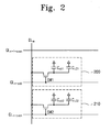
- FIG. 2 is an equivalent schematic circuit diagram of a pixel of the LCD according to the exemplary embodiment of the present invention shown in FIG. 1 .
- a pixel includes a first sub-pixel 200 and a second sub-pixel 210.
- the first sub-pixel 200 includes a first switching device SW1, a first storage capacitor C st1 , and a first liquid crystal capacitor C LC1 .
- the first switching device SW1 includes a control terminal connected to an n-th odd-numbered gate line GL n-odd , an input terminal connected to an m-th data line DL m , and an output terminal connected to the first liquid crystal capacitor C LC1 and to the first storage capacitor C st1 .
- the first storage capacitor C st1 maintains an electric charge charged into the first liquid crystal capacitor C LC1 .
- the first liquid crystal capacitor C LC1 is charged with a data voltage applied to the m-th data line DL m connected to the input terminal of the first switching device SW1.
- the gate signal is defined as a signal which has a voltage level sufficient to turn on the first switching device SW1.
- the data voltage charged in the first liquid crystal capacitor C LC1 is maintained by the first storage capacitor C st1 during one frame.
- the second sub-pixel 210 includes a second switching device SW2, a second liquid crystal capacitor C LC2 , and a second storage capacitor C st2 . Since the second sub-pixel 210 has substantially the same structure and function as the first sub-pixel 200, a repetitive detailed description of the second sub-pixel 210 will be omitted.
- the n-th even-numbered gate line GL n-even connected to the second switching device SW2 is disposed adjacent to, e.g., subsequent to, the n-th odd-numbered gate line GL n-odd connected to the first switching device SW1, as shown in FIG. 2 .
- the first liquid crystal capacitor C LC1 of the first sub-pixel 200 and the second liquid crystal capacitor C LC2 of the second sub-pixel 210 are charged with different voltages from each other at different times during one frame, as described in further detail below with reference to FIG. 3 . Since the voltage charged in the first sub-pixel 200 is different from the voltage charged in the second sub-pixel 210, distortion of a displayed image at different viewing angles is substantially reduced or effectively prevented in the LCD 160 according to an exemplary embodiment of the present invention.
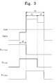
- FIG. 3 is a waveform timing diagram of a data signal and a gate signal applied to the pixel of the LCD according to the exemplary embodiment of the present invention shown in FIG. 2 .
- a gate-on signal e.g., a gate signal having a high value
- a gate signal having a high value is applied to both the n-th odd-numbered gate line GL n-odd and the n-th even-numbered gate line GL n-even connected to the first sub-pixel 200 and the second sub-pixel 210, respectively, during a first time interval t1, and a gray-scale data voltage Vdata having a high positive value with respect to a common voltage Vcom is applied to the m-th data line DL m . Therefore, the first sub-pixel 200 and the second sub-pixel 210 are charged with the gray-scale data voltage having the high positive value.
- the gate-on signal is not applied to the n-th odd-numbered gate line GL n-odd connected to the first sub-pixel 200, while the gate-on signal is still applied to the n-th even-numbered gate line GL n-even connected to the second sub-pixel 210.
- a gray-scale data voltage Vdata having a value less than the high positive data value of the gray-scale data voltage Vdata in the first time interval t1 but greater than the common voltage Vcom is applied to the m-th data line D m connected to the first sub-pixel 200 and the second sub-pixel 210 during the second time interval t2.
- the lower gray-scale data voltage Vdata e.g., the gray-scale data voltage Vdata having a value less than the high positive data value of the gray-scale data voltage Vdata in the first time interval t1 but greater than the common voltage Vcom
- the first sub-pixel 200 maintains the relatively high positive gray-scale data voltage charged therein during the first time interval t1.
- the first time interval t1 and the second time interval t2 define one horizontal scanning period 1 H.
- the first sub-pixel 200 is charged with the data voltage Vdata having a high value while the second sub-pixel 210 is charged with the data voltage Vdata having the relatively low value, during a specific time interval, e.g., the second time interval t2, of one horizontal scanning period 1 H, as illustrated in FIG. 3 .
- the gate-on signal is applied to the n-th odd-numbered gate line GL n-odd and a previous even-numbered gate line GL n-1-even during a pre-first time interval t0.
- the gray-scale data voltage Vdata having the relatively low value e.g., the gray-scale data voltage Vdata having a value less than the high positive data value of the gray-scale data voltage Vdata in the first time interval t1 but greater than the common voltage Vcom
- a second sub-pixel 210 of a pixel scanned at a time adjacent and prior to the pixel which is scanned during the first time interval t1 and the second time interval t2 hereinafter referred to as a "present pixel").
- the first sub-pixel 200 of the present pixel is also charged with the gray-scale data voltage Vdata having the relatively low value.
- a polarity of the gray scale data voltage Vdata is inverted every row (referred to as row inversion). Therefore, the gray-scale data voltage Vdata having the relatively low value which is charged in the second sub-pixel 210 of the pixel adjacent and prior to the present pixel has a negative polarity with respect to the common voltage, while the first sub-pixel 200 and the second sub-pixel 210 of the present pixel are each charged by the gray-scale data voltage Vdata having a positive polarity, as shown in FIG. 3 .
- the gray-scale data voltage Vdata having the relatively low negative polarity value is precharged in the first sub-pixel 200 of the present pixel, since the gate-on signal is applied to the n-th odd-numbered gate line GL n-odd during the pre-first time interval t0, prior to and adjacent to the first time interval t1. Further, the gray-scale data voltage Vdata having the relatively low negative polarity value has a voltage level relatively higher, e.g., closer to the common voltage Vcom, than that of the high gray-scale data voltage Vdata having the negative polarity in a time period (not labeled) adjacent and prior to the pre-first tie period T0 in FIG. 3 .
- the first sub-pixel 200 of the present pixel when the first sub-pixel 200 of the present pixel is precharged by the gray-scale data voltage Vdata having the relatively low negative polarity value, the first sub-pixel 200 of the present pixel reaches the gray-scale data voltage Vdata having the relatively high positive polarity value in the first time interval t1 faster than in a case when the first sub-pixel 200 of the present pixel is precharged by the gray-scale data voltage Vdata having the relatively high negative polarity.
- the gray-scale data voltage Vdata having the relatively high value and the gray-scale voltage Vdata having the relatively low value are applied to the first sub-pixel 200 and the second sub-pixel 210, respectively, thereby substantially reducing or effectively eliminating distortion of a displayed image at different viewing angles, thereby substantially improving a range of viewing angles of the LCD 160.
- the first sub-pixel 200 of the present pixel is precharged, a charging time of the first sub-pixel 200 of the present pixel is reduced, thereby improving a response time of the LCD 160.
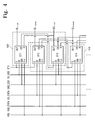
- FIG. 4 is a block diagram of a gate driver of the LCD according to the exemplary embodiment of the present invention shown in FIG. 1 .
- the gate driver 110 ( FIG. 1 ) according to an exemplary embodiment includes a plurality of stages, including a first stage ST1, a second stage ST2, a third stage ST3 and a fourth stage ST4, as shown in FIG. 4 .
- the gate driver 110 is divided into a first gate driver part 400 and a second gate driver part 410. More specifically, the first gate driver part 400 includes odd-numbered first stage ST1 and third stage ST3, while the second gate driver part 410 includes even-numbered second stage ST2 and the fourth stage ST4.
- the first gate driver part 400 provides gate signals to the odd-numbered gate lines GL 1-odd and GL 2-odd
- the second gate driver 410 provides gate signals to the even-numbered gate lines GL 1-even and GL 2-even .
- Each of the first stage ST1, the second stage ST2, the third stage ST3 and the fourth stage ST4 includes a set terminal S, a gate voltage terminal Vin, a first clock terminal CK, a second clock terminal CKB, a reset terminal R, a gate output terminal OUT and a carry output terminal CR.
- Each of the odd-numbered stages receives a carry signal output from a carry output terminal CR of an adjacent previous odd-numbered stage through the set terminal S thereof and receives a gate signal output from the gate output terminal OUT of an adjacent subsequent odd-numbered stage through the reset terminal R thereof.
- the first stage ST1 of the first gate driver part 400 receives a scanning start signal STV through the set terminal S thereof in lieu of a carry signal from a previous odd-numbered stage.
- each odd-numbered stage e.g., the first stage ST1 and the third stage ST3 receives a first clock signal CK_ODD and a second clock signal CKB_ODD alternatively applied to the first clock terminal CK and the second clock terminal CKB, respectively, and receives a gate-off voltage VSS through the gate voltage terminal Vin thereof. More specifically, when the first clock signal CK_ODD is applied to the first clock terminal CK, the second clock signal CKB_ODD is applied to the second clock terminal CKB of a given odd-numbered stage. Further, the first clock signal CK_ODD and the second clock signal CKB_ODD are alternately applied to the first clock terminal CK and the second clock terminal CKB of each consecutive odd-numbered stage, as shown in FIG. 4 .
- each even-numbered stage receives a carry signal output from a carry output terminal CR of an adjacent previous even-numbered stage through the set terminal S thereof and receives a gate signal output from the gate output terminal OUT of an adjacent subsequent even-numbered stage through the reset terminal R thereof.
- the second stage ST2 of the second gate driver part 400 receives the scanning start signal STV through the set terminal S thereof in lieu of a carry signal from a previous even-numbered stage.
- each even-numbered stage e.g., the second stage ST2 and the fourth stage ST4 receives a third clock signal CK_EVEN and a fourth clock signal CKB_EVEN alternatively applied to the first clock terminal CK and the second clock terminal CKB, respectively, and receives the gate-off voltage VSS through the gate voltage terminal Vin thereof.
- the third clock signal CK_EVEN is applied to the first clock terminal CK
- the fourth clock signal CKB_EVEN is applied to the second clock terminal CKB of a given even-numbered stage.
- the third clock signal CK_EVEN and the fourth clock signal CKB_EVEN are alternately applied to the first clock terminal CK and the second clock terminal CKB, respectively, of each even-numbered stage.
- the first to fourth clock signals CK_ODD, CKB_ODD, CK_EVEN and CKB_EVEN respectively, have a high voltage level substantially equal to a voltage level which turns on a switching device of the pixel of the LCD 160, as well as a low voltage level substantially equal to a voltage level which turns off the switching device thereof.
- the scanning start signal STV, and the first to fourth clock signals CK_ODD, CKB_ODD, CK_EVEN, and CKB_EVEN, respectively, are included in the second control signal CN2 output from the timing controller 140 to the gate driver 110 ( FIG. 1 ), but alternative exemplary embodiments are not limited thereto.
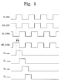
- FIG. 5 is a waveform timing diagram of first to fourth clock signals and first to fourth gate signals of the gate driver according to the exemplary embodiment of the present invention shown in FIG. 4 .
- the first to fourth clock signals CK_ODD, CKB_ODD, CK_EVEN, and CKB_EVEN respectively, have a substantially equal period.
- a phase difference between the first clock signal CK_ODD and the second clock signal CKB_ODD is substantially 180 degrees, e.g., one half of one period, and a phase difference between the third clock signal CK_EVEN and the fourth clock signal CKB_EVEN is substantially 180 degrees.
- a phase difference ⁇ t between the first clock signal CK_ODD and the third clock signal CK_EVEN is substantially 90 degrees, e.g., substantially one half of one period
- a phase difference ⁇ t between the second clock signal CKB_ODD and the fourth clock signal CKB_EVEN is substantially 90 degrees.
- the first gate driver part 400 provides gate signals corresponding to high periods of the first clock signal CK_ODD and the second clock signal CKB_ODD to the first odd-numbered gate line GL 1-odd and the first even-numbered gate line GL 2-odd , respectively.
- the second gate driver part 410 provides gate signals corresponding to high periods of the third clock signal CK_EVEN and the fourth clock signal CKB_EVEN to the first even-numbered gate line G 1-even and the first even-numbered gate line GL 2-even , respectively, as shown in FIG. 5 .
- the gate signal applied to the first odd-numbered gate line GL 1-odd overlaps the gate signal applied to the first even-numbered gate line GL 1-even during a specific time interval, e. g., one quarter of one period, as shown in FIG. 5 .
- the gate signal applied to the second odd-numbered gate line GL 2-odd overlaps the gate signal applied to the second even-numbered gate line GL 2-even during the specific time interval, e. g., one quarter of one period.
- a polarity of a data voltage applied to a given pixel is inverted every frame and is opposite to a polarity of a data voltage applied to an adjacent pixel to prevent deterioration of the liquid crystal.
- a given gate signal overlaps with a gate signal applied to an adjacent gate line, thereby achieving a precharge effect. More specifically, the precharge effect is achieved during an overlapping time interval wherein an odd-numbered gate signal overlaps a previous even-numbered gate signal, and a charge in the corresponding pixel is maintained until the respective gate signal is turned off after the associated precharge effect is achieved.
- the pixel of the LCD 160 includes the first sub-pixel 200 and the second sub-pixel 210, wherein the first sub-pixel 200 is connected to an odd-numbered gate line and the second sub-pixel 210 is connected to an even-numbered gate line, as shown in FIG. 2 .
- Vdata gray-scale data voltage
- the first sub-pixel 200 of an adjacent subsequent pixel is precharged with the gray-scale data voltage Vdata having the relatively low negative polarity value when the gray-scale data voltage Vdata having the relatively low negative polarity value is applied to the second sub-pixel 210 of an adjacent previous pixel. Since the adjacent subsequent pixel is charged with the gray-scale data voltage Vdata having the relatively high negative polarity value during the previous frame, the precharge is achieved when the next pixel is charged with the gray-scale data voltage Vdata having the relatively low negative polarity value.
- the second sub-pixel 210 charged with the gray-scale data voltage Vdata having the relatively low negative polarity value in the previous frame is precharged with the gray-scale data voltage Vdata having the relatively high positive polarity value.
- the first clock signal CK_ODD and the third clock signal CK_EVEN have a phase difference of substantially 90 degrees therebetween and the second clock signal CKB_ODD and the fourth clock signal CKB_EVEN also have a phase difference of substantially 90 degrees therebetween, but alternative exemplary embodiments are not limited thereto.
- the phase difference between the first clock signal CK_ODD and the third clock signal CK_EVEN and/or the phase difference between the second clock signal CKB_ODD and the fourth clock signal CKB_EVEN may be set to different and various values based on a desired precharging time.
- a gate signal output from the first gate driver part 400 may have a voltage amplitude different from a voltage amplitude of a gate signal output from the second driver part 410 in order to prevent a kickback voltage, e.g., a shift in pixel voltage, which may be generated between the first sub-pixel 200 charged with the high gray-scale data voltage and the second sub-pixel 210 charged with the low gray-scale data voltage, as will now be described in further detail with reference to FIG. 6 .
- a kickback voltage e.g., a shift in pixel voltage
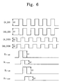
- FIG. 6 is a waveform timing diagram of first to fourth clock signals and first to fourth gate signals of a gate driver of an LCD according to an alternative exemplary embodiment of the present invention.
- the first clock signal CK_ODD and the second clock signal CKB_ODD have a first clock amplitude A1, while the third clock signal CK_EVEN and the fourth clock signal CKB_EVEN have a second clock amplitude A2 smaller than the first clock amplitude A1.
- a phase difference between the first clock signal CK_ODD and the second clock signal CKB_ODD is substantially 180 degrees, while a phase difference between the third clock signal CK_EVEN and the fourth clock signal CKB_EVEN is substantially 180 degrees, as shown in FIG. 6 .
- the first clock signal CK_ODD and the third clock signal CK_EVEN have a phase difference of substantially 90 degrees therebetween
- the second clock signal CKB_ODD and the fourth clock signal CKB_EVEN also have a phase difference of substantially 90 degrees therebetween.
- a gate signal output from the first gate driver part 400 and applied to odd-numbered gate lines GL 1-odd and GL 2-odd has a first gate voltage amplitude V1 based on the first clock signal CK_ODD and the second clock signal CKB_ODD
- a gate signal output from the second gate driver part 410 and applied to even-numbered gate lines GL 1-even and GL 2-even has a second gate voltage amplitude V2 different than the first gate voltage amplitude V1.
- the first gate voltage amplitude V1 of the gate signal output from the first gate driver part 400 is greater than the second gate voltage amplitude V2 of the gate signal output from the second gate driver part 410, as shown in FIG. 6 .
- Relationships and values of the amplitudes of the first to fourth clock signals CK_ODD, CKB_ODD, CK_EVEN, and CKB_EVEN, respectively, in alternative exemplary embodiments of the present invention are not limited to those shown in FIG. 6 . Rather, the amplitudes of the first to fourth clock signals CK_ODD, CKB_ODD, CK_EVEN, and CKB_EVEN, respectively, may be set to different and various values. As a result, a voltage amplitude of a sub-pixel, e.g., the first sub-pixel 200 and/or the second sub-pixel 210, is sufficiently charged during operation of the LCD 160 according to an exemplary embodiment of the present invention.
- a voltage amplitude of the gate signal applied to a sub-pixel which may be charged insufficiently, e.g., the first sub-pixel 200, is set to relatively high value with respect to a voltage amplitude of the gate signal applied to the other sub-pixel, e.g., the second sub-pixel 210, thereby reducing kickback voltage difference between the first sub-pixel 200 and the second sub-pixel 210.
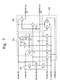
- FIG. 7 is a schematic circuit diagram of a single stage of the gate driver according to the exemplary embodiment of the present invention shown in FIG. 4 .
- the stages of the gate driver 110 ( FIG. 1 ), e.g., the first stage ST1, the second stage ST2, the third stage ST3 and the fourth stage ST4 ( FIG. 4 ), each have substantially the same configuration and function, as described in greater detail above. Therefore only one stage is illustrated in further detail in FIG. 7 , and only one stage will now be described in further detail, in order to avoid redundancy.
- a single stage includes an input part 620, a pull-up driving part 630, a pull-down driving part 640 and an output part 650.
- the single stage further includes first to fourteenth transistors T1 to T14, respectively, first to third capacitors C1 to C3, respectively, and first to fourth nodes J1 to J4, respectively.
- the input part 620 includes the fifth, tenth and eleventh transistors T5, T10 and T11, respectively, connected in series with each other between a set terminal S of the single stage and a gate voltage terminal Vin of the single stage.
- Gates of the fifth and eleventh transistors T5 and T11, respectively, are connected to a second clock terminal CKB of the single stage, and a gate of the tenth transistor T10 is connected to a first clock terminal CK of the single stage.
- a contact point between the eleventh transistor T11 and the tenth transistor T10 is connected to the first node J1, and a contact point between the tenth transistor T10 and the fifth transistor T5 is connected to the second node J2, as shown in FIG. 7 .
- the pull-up driving part 630 includes the fourth transistor T4 connected between the set terminal S of the single stage and the first node J1, the twelfth transistor T12 connected between the first clock terminal CK and the third node J3, and the seventh transistor T7 connected between the first clock terminal CK and the fourth node J4.
- the fourth transistor T4 includes a gate and a drain commonly connected to the set terminal S, and a source connected to the first node J1.
- the twelfth transistor T12 includes a gate and a drain commonly connected to the first clock terminal CK, e.g., the fifth node J5, and a source connected to the third node J3.
- the seventh transistor T7 includes a gate connected to the third node J3 and connected to the first clock terminal CK, e.g., the fifth node J5, through the first capacitor C1, a drain connected to the first clock terminal CK, and a source connected to the fourth node J4.
- the pull-up driving part 630 further includes the second capacitor C2 connected between the third node J3 and the fourth node J4.
- the pull-down driving part 640 includes the sixth, ninth, thirteenth, eighth, third and second transistors T6, T9, T13, T8, T3 and T2, respectively, each receiving the gate-off voltage VSS to a source thereof through the gate voltage terminal Vin of the single stage.
- the sixth transistor T6 and the ninth transistor T9 output the gate-off voltage V SS through a drain thereof to the first node J1
- the thirteenth transistor T13 outputs the gate-off voltage V SS through a drain thereof to the third node J3
- the eighth transistor T8 outputs the gate-off voltage V SS through a drain thereof to the fourth node J4
- the third transistor T3 and the second transistor T2 output the gate-off voltage V SS through a drain thereof to the second node J2.
- the sixth transistor T6 includes a gate connected to a frame reset terminal FR of the single stage and a drain connected to the first node J1
- the ninth transistor T9 includes a gate connected to a reset terminal R of the single stage and a drain connected to the first node J1.
- Gates of the thirteenth and eighth transistors T13 and T8, respectively, are commonly connected to the second node J2, and drains of the thirteenth and eighth transistors T13 and T8, respectively, are connected to the third node J3 and the fourth node J4, respectively.
- the third transistor T3 includes a gate connected to the fourth node J4 and a drain connected to the second node J2.
- the second transistor T2 includes a gate connected to the reset terminal R of the single stage and a drain connected to the second node J2.
- the output part 650 includes the first and fourteenth transistors T1 and T14, respectively.
- the first transistor T1 includes a gate connected to the first node J1, a drain connected to the first clock terminal CK of the single stage, and a source connected to an output terminal OUT of the single stage, through which a gate signal Gout is output, and to the second node J2.
- the fourteenth transistor T14 includes a gate connected to the first node J1, a drain connected to the first clock terminal CK of the single stage, and a source connected to a carry terminal CR of the single stage, through which a carry signal Cout is output.
- the output part 650 further includes the third capacitor C3 connected between the first node J1 and the second node J2.
- each of the first to fourteenth transistors T1 to T14 is an NMOS transistor, as shown in FIG. 7 , but alternative exemplary embodiments are not limited thereto.
- any or all of the first to fourteenth transistors T1 to T14, respectively may be a PMOS transistor.
- the first, second and third capacitors C1, C2 and C3, respectively may be implemented as a parasitic capacitance formed between a gate, drain, and/or source of one or more of the first to fourteenth transistors T1 to T14, respectively, but alternative exemplary embodiments are not limited to the foregoing description.
- a voltage corresponding to a high level of a clock signal applied to the first clock terminal CK of the single stage has a level substantially the same as a level of voltage which turns on switching devices of the LCD 160, and will hereinafter be referred to as a high voltage.
- a voltage corresponding to a low level of a clock signal applied to the second clock terminal CKB of the single stage e.g., the second clock signal CKB_ODD ( FIG. 4 )
- has a level substantially equal to a level of the gate-off voltage VSS and will hereinafter be referred to as a low voltage.
- the gates signal Gout and the carry signal Cout output through the output terminal OUT and the carry terminal CR, respectively, are at the low voltage level. Further, the third capacitor C3 is charged to a voltage substantially corresponding to a difference between the high voltage and the low voltage.
- the second node J2 remains at the logic low state, and the tenth, ninth, twelfth, thirteenth, eighth, and second transistors T10, T9, T12, T13, T8, and T2, respectively, are turned off.
- the eleventh and fifth transistors T11 and T5 are turned off.
- the clock signal applied to the first clock terminal CK of the current single stage transitions to a logic high state, and an output voltage of the first transistor T1 and a voltage of the second node J2 therefore transition to the high voltage.
- the high voltage is applied to the gate of the tenth transistor T10, the electric potential difference between the gate and source of the tenth transistor T10 is substantially zero because the source of the tenth transistor T10 connected to the second node J2 is at the high voltage.
- the tenth transistor T10 remains in a turned-off state. Accordingly, the first node J1 is in a floating state and an electric potential of the first node J1 increases to substantially the high voltage charged to the third capacitor C3.
- the clock signal applied to the first clock terminal CK of the current single stage and the second node J2 have the high voltage, and the twelfth, thirteenth and eighth transistors T12, T13, and T8, respectively, are thereby turned on.
- the twelfth transistor T12 and the thirteenth transistor T13 are connected in series with each other between the high voltage and the low voltage, e.g., between the first clock terminal CK and the gate voltage terminal Vin of the current single stage, the third node J3 is at an electric potential substantially corresponding to a voltage value substantially equal to a value determined by turn-on resistance values of the twelfth and thirteenth transistors T12 and T13, respectively, e.g., a value voltage-divided between the twelfth and thirteenth transistors T12 and T13, respectively.
- a turn-on resistance value of the thirteenth transistor T13 is about ten thousand times greater than a turn-on resistance value of the twelfth transistor T12, and the voltage value of third node J3 is therefore substantially equal to the high voltage.
- the seventh transistor T7 is turned on. Since the seventh transistor T7 is connected in electrical series with the eighth transistor T8 through the fourth node J4, the fourth node J4 has an electric potential substantially corresponding to a voltage value voltage-divided by turn-on resistance values of the seventh and eighth transistors T7 and T8, respectively.
- the turn-on resistance values of the seventh and eight transistors T7 and T8 are substantially the same value, and the fourth node J4 therefore has an electric potential corresponding to an intermediate voltage value substantially between the high voltage and the low voltage.
- the third transistor T3 is maintained in a turned off state.
- the gate signal Gout of a subsequent single stage, applied through the reset terminal R of the current single stage is at a logic low level, and the ninth and second transistors T9 and T2, respectively, are maintained in a turned off state. Accordingly, the gate signal Gout and the carry signal Cout having the high voltage are output through the output terminal OUT and the carry terminal CR, respectively, of the current single stage.
- the first capacitor C1 is charged to a voltage substantially corresponding to an electric potential difference between the third node J3 and the fifth node J5, while the second capacitor C2 is charged to a voltage substantially corresponding to an electric potential difference between the fourth node J4 and the fifth node J5. Further, a voltage at the third node J3 is lower than a voltage at the fifth node J5, since the clock signal applied to the first clock terminal CK, e.g., to the fifth node J5, of the current single stage is at a logic high level.
- the ninth and second transistors T9 and T2, respectively are turned on, thereby applying the low voltage to the first and second nodes J1 and J2, respectively.
- a voltage at the first node J1 drops to the low voltage level while the third capacitor C3 discharges.
- a predetermined time elapses before the voltage at the first node J1 transitions to the low voltage level, due to a discharging time of the third capacitor C3.
- the first and fourteenth transistors T1 and T14 are maintained in a turned on state during a portion of the predetermined time after to the gate signal Gout of the subsequent single stage transitions to a logic high level, e.g., the gate signal Gout and the carry signal Cout of the current single stage do not transition to the low voltage level until the predetermined time elapses.
- the fourteenth transistor T14 is turned off and the carry terminal CR is electrically disconnected from the first clock terminal CK of the current single stage, and the carry signal Cout is thereby floated, e.g., is maintained at substantially the low voltage level.
- the first transistor T1 is turned off, the output terminal OUT of the current single stage receives the low voltage through the second transistor T2, and the low voltage is thereby continuously output from the output terminal OUT of the current single stage.
- the third node J3 When the twelfth and thirteenth transistors T12 and T13, respectively, are turned off, the third node J3 is in a floating state. A voltage at the fifth node J5 is thereby lowered below a voltage at the fourth node J4 while a voltage at the third node J3 is lowered below a voltage at the fifth node J5, thereby turning off the seventh transistor T7. Substantially simultaneously, the third transistor T3 is turned off and a voltage at the fourth node J4 is lowered, and the third transistor T3 is therefore maintained in a turned off state. Further, the clock signal applied to the first clock terminal CK of the current single stage is at the low voltage and is applied to the gate of the tenth transistor T10. A voltage at the second node J2 therefore transitions to a logic low level, to thereby maintain the tenth transistor T10 in a turned off state.
- the tenth transistor T10 When the clock signal having the high voltage level applied to the first clock terminal of the current single stage is applied to the gate of the tenth transistor T10, the tenth transistor T10 is turned on and the voltage level at the second node J2, e.g., the low voltage, is thereby applied to the first node J1.
- the first clock terminal CK is connected to the drains of the thirteenth and fourteenth transistors T13 and T14, respectively.
- the thirteenth transistor T13 has a large size compared with the other transistors, and a parasitic capacitance between the gate and the drain of the thirteenth transistor T13 is thereby relatively large, and a voltage variation of the drain influences a gate voltage thereof.
- the thirteenth transistor T13 is turned on by the gate voltage increased by the parasitic capacitance between the gate and the drain thereof.
- the gate voltage of the thirteenth transistor T13 is maintained at the low voltage level, thereby preventing the thirteenth transistor T13 from turning on.
- a voltage at the first node J1 is maintained at the low voltage level until the carry signal Cout from the previous single stage transitions to a logic high level, and the voltage of the second node J2 is maintained at the low voltage level, through the third transistor T3, when the clock signal applied to the first clock terminal CK of the current single stage is at a logic high state and the clock signal applied to the second clock terminal CKB of the current single stage is at a logic low state.
- the voltage at the second node J2 is maintained at the low voltage through the fifth transistor T5 when the clock signal applied to the first clock terminal CK of the current single stage transitions back to a logic low level and the clock signal applied to he second stage CKB of the current single stage transitions back to a logic high level.
- the sixth transistor T6 applies the gate-off voltage VSS to the first node J1 in response to an initializing signal applied through the frame reset terminal FR of the current single stage, and a voltage at the first node J1 is thereby set to the low voltage level again.
- the initializing signal is the carry signal Cout generated from a last single stage among the single stages of the gate driver 110, e.g., the single stage associated with a last odd-numbered gate line GL n-odd or a last even-numbered gate line GL n-even , but alternative exemplary embodiments are not limited thereto.
- the second gate driver part 410 may generate the carry signal Cout and the gate signal Gout based on a previous carry signal and a next gate signal, respectively, obtained by synchronizing with a clock signal, e.g., the third clock signal CK_EVEN and/or the fourth clock signal CKB_EVEN, but alternative exemplary embodiments are not limited thereto.
- a clock signal e.g., the third clock signal CK_EVEN and/or the fourth clock signal CKB_EVEN, but alternative exemplary embodiments are not limited thereto.
- an LCD display apparatus As described herein, in an LCD display apparatus according to an exemplary embodiment of the present invention, distortion of a displayed image at different viewing position is substantially reduced or effectively prevented, thereby substantially improving a display quality of the LCD display apparatus. Further, a sub-pixel is precharged in the LCD display apparatus according to an exemplary embodiment, thereby reducing a charging time of the sub-pixel and improving a response time of the LCD display apparatus. In addition, a gate driver is directly disposed on a display panel, thereby improving a manufacturing efficiency of the LCD display apparatus.
- a method of driving a display apparatus having a pixel having a first sub-pixel and a second sub-pixel includes: applying a first gate signal at a high logic state and a data signal at a first voltage level to the first sub-pixel during a first time interval of a horizontal scanning period; applying a second gate signal at a high logic state and a data signal at the first voltage level to the second sub-pixel during the first time interval of the horizontal scanning period; and applying the second gate signal at a high logic state and a data signal at a second voltage level to the second sub-pixel during a second time interval of the horizontal scanning period.
- the second voltage level is lower than the first voltage level, and at least one of a previous first gate signal and a previous second gate signal temporally overlap at least one of a current first gate signal and a current second gate signal, respectively.
- An amplitude of the first gate signal is different than an amplitude of the second gate signal.
Landscapes
- Engineering & Computer Science (AREA)
- Physics & Mathematics (AREA)
- General Physics & Mathematics (AREA)
- Crystallography & Structural Chemistry (AREA)
- Theoretical Computer Science (AREA)
- Chemical & Material Sciences (AREA)
- Computer Hardware Design (AREA)
- Nonlinear Science (AREA)
- Mathematical Physics (AREA)
- Optics & Photonics (AREA)
- Control Of Indicators Other Than Cathode Ray Tubes (AREA)
- Liquid Crystal (AREA)
- Shift Register Type Memory (AREA)
- Liquid Crystal Display Device Control (AREA)
Applications Claiming Priority (1)
| Application Number | Priority Date | Filing Date | Title |
|---|---|---|---|
| KR1020070079099A KR101448904B1 (ko) | 2007-08-07 | 2007-08-07 | 표시장치 |
Publications (1)
| Publication Number | Publication Date |
|---|---|
| EP2023331A1 true EP2023331A1 (de) | 2009-02-11 |
Family
ID=39551817
Family Applications (1)
| Application Number | Title | Priority Date | Filing Date |
|---|---|---|---|
| EP08006206A Pending EP2023331A1 (de) | 2007-08-07 | 2008-03-29 | Anzeigevorrichtung und Verfahren zu ihrer Ansteuerung |
Country Status (6)
| Country | Link |
|---|---|
| US (1) | US8698722B2 (de) |
| EP (1) | EP2023331A1 (de) |
| JP (1) | JP5269490B2 (de) |
| KR (1) | KR101448904B1 (de) |
| CN (1) | CN101364391A (de) |
| TW (1) | TWI462074B (de) |
Cited By (3)
| Publication number | Priority date | Publication date | Assignee | Title |
|---|---|---|---|---|
| CN109192170A (zh) * | 2018-10-23 | 2019-01-11 | 惠科股份有限公司 | 显示面板的馈穿补偿方法及装置、显示装置 |
| US11315954B2 (en) | 2009-11-06 | 2022-04-26 | Semiconductor Energy Laboratory Co., Ltd. | Semiconductor device and manufacturing method thereof |
| US11417261B2 (en) | 2018-09-27 | 2022-08-16 | Hefei Xinsheng Optoelectronics Technology Group Co., Ltd. | Gate driving unit circuit, gate driving circuit, display device and driving method for improving charge rate |
Families Citing this family (44)
| Publication number | Priority date | Publication date | Assignee | Title |
|---|---|---|---|---|
| KR20070013013A (ko) * | 2005-07-25 | 2007-01-30 | 삼성전자주식회사 | 표시 장치 |
| TWI404024B (zh) * | 2008-06-30 | 2013-08-01 | Innolux Corp | 畫素組、平面顯示面板及平面顯示裝置的驅動方法 |
| KR101607510B1 (ko) * | 2008-11-28 | 2016-03-31 | 삼성디스플레이 주식회사 | 게이트 구동 방법 및 회로와, 이를 갖는 표시장치 |
| TWI413050B (zh) * | 2009-03-17 | 2013-10-21 | Au Optronics Corp | 高可靠度閘極驅動電路 |
| CN101783128B (zh) * | 2010-04-02 | 2012-08-08 | 福州华映视讯有限公司 | 液晶显示器的驱动方法 |
| KR101097351B1 (ko) * | 2010-05-06 | 2011-12-23 | 삼성모바일디스플레이주식회사 | 주사 구동 회로 및 이를 이용한 표시 장치 |
| WO2011155766A2 (ko) * | 2010-06-08 | 2011-12-15 | 엘지전자 주식회사 | 영상 처리 방법 및 그에 따른 영상 표시 장치 |
| TWI451176B (zh) * | 2011-05-23 | 2014-09-01 | Au Optronics Corp | 液晶顯示器及用來對液晶顯示器的像素充放電的方法 |
| TWI449018B (zh) * | 2011-09-13 | 2014-08-11 | Au Optronics Corp | 掃描式背光模組、立體影像顯示裝置、掃描式背光模組的驅動方法、立體影像顯示裝置的顯示方法 |
| US8730229B2 (en) * | 2011-09-28 | 2014-05-20 | Apple Inc. | Devices and methods for zero-bias display turn-off using VCOM switch |
| CN102650779A (zh) * | 2011-09-30 | 2012-08-29 | 北京京东方光电科技有限公司 | 液晶显示器 |
| KR102011985B1 (ko) | 2012-07-23 | 2019-08-20 | 삼성디스플레이 주식회사 | 표시 장치 및 그 구동 방법 |
| KR102034140B1 (ko) * | 2013-01-23 | 2019-10-21 | 삼성디스플레이 주식회사 | 게이트 구동부 및 이를 포함하는 표시 장치 |
| CN103337232B (zh) * | 2013-05-25 | 2015-11-18 | 福建华映显示科技有限公司 | 闸极驱动电路 |
| KR20150005259A (ko) | 2013-07-05 | 2015-01-14 | 삼성디스플레이 주식회사 | 표시 패널 및 이를 포함하는 표시 장치 |
| TWI512701B (zh) * | 2013-08-08 | 2015-12-11 | Novatek Microelectronics Corp | 液晶顯示器及其閘極驅動器 |
| KR20150070683A (ko) * | 2013-12-17 | 2015-06-25 | 삼성디스플레이 주식회사 | 액정 표시 장치 및 이의 구동 방법 |
| CN103680454A (zh) * | 2013-12-20 | 2014-03-26 | 深圳市华星光电技术有限公司 | 显示装置及显示驱动方法 |
| KR20150077872A (ko) * | 2013-12-30 | 2015-07-08 | 삼성디스플레이 주식회사 | 표시 패널 구동 방법, 이 표시 패널 구동 방법을 수행하는 표시 패널 구동 장치 및 이 표시 패널 구동 장치를 포함하는 표시 장치 |
| KR102335113B1 (ko) * | 2014-12-22 | 2021-12-03 | 삼성디스플레이 주식회사 | 표시 장치 및 그 구동 방법 |
| KR102239581B1 (ko) * | 2015-01-26 | 2021-04-14 | 삼성디스플레이 주식회사 | 표시 장치 |
| CN105185339B (zh) * | 2015-10-08 | 2017-12-29 | 京东方科技集团股份有限公司 | 移位寄存器单元、栅线驱动装置以及驱动方法 |
| CN105204249B (zh) * | 2015-10-29 | 2018-07-17 | 深圳市华星光电技术有限公司 | 阵列基板上的扫描驱动电路及阵列基板 |
| CN105304041B (zh) * | 2015-11-06 | 2019-03-22 | 深圳市华星光电技术有限公司 | 一种扫描驱动装置 |
| US10528165B2 (en) * | 2016-04-04 | 2020-01-07 | Semiconductor Energy Laboratory Co., Ltd. | Display device, display module, and electronic device |
| KR102581368B1 (ko) * | 2016-07-07 | 2023-09-22 | 삼성디스플레이 주식회사 | 표시 패널의 구동 방법 및 이를 수행하기 위한 표시 장치 |
| KR102609509B1 (ko) * | 2016-11-17 | 2023-12-04 | 엘지디스플레이 주식회사 | 외부 보상용 표시장치와 그 구동방법 |
| CN106683626A (zh) * | 2016-12-16 | 2017-05-17 | 深圳市华星光电技术有限公司 | 一种液晶显示面板的驱动方法及驱动电路 |
| CN107068108B (zh) * | 2017-06-26 | 2019-06-28 | 惠科股份有限公司 | 显示面板的驱动方法及装置、显示装置 |
| KR102448354B1 (ko) * | 2017-08-24 | 2022-09-28 | 삼성디스플레이 주식회사 | 표시 장치 |
| TWI633533B (zh) * | 2017-09-21 | 2018-08-21 | 友達光電股份有限公司 | 液晶顯示裝置 |
| CN109935196B (zh) * | 2018-02-14 | 2020-12-01 | 京东方科技集团股份有限公司 | 移位寄存器单元、栅极驱动电路、显示装置以及驱动方法 |
| CN109935208B (zh) | 2018-02-14 | 2021-03-02 | 京东方科技集团股份有限公司 | 移位寄存器单元、栅极驱动电路、显示装置以及驱动方法 |
| KR102647372B1 (ko) * | 2018-07-13 | 2024-03-13 | 삼성디스플레이 주식회사 | 표시 장치 및 그 제조 방법 |
| CN109935209B (zh) * | 2018-07-18 | 2021-02-02 | 京东方科技集团股份有限公司 | 移位寄存器单元、栅极驱动电路、显示装置及驱动方法 |
| KR102568650B1 (ko) * | 2018-10-18 | 2023-08-23 | 삼성디스플레이 주식회사 | 통신 장치, 그것을 이용한 표시 장치 검사 시스템 및 검사 방법 |
| TWI685831B (zh) * | 2019-01-08 | 2020-02-21 | 友達光電股份有限公司 | 畫素電路及其驅動方法 |
| CN109801587B (zh) * | 2019-04-10 | 2021-11-23 | 京东方科技集团股份有限公司 | 驱动信号提供方法和提供电路、显示装置 |
| US11250753B2 (en) * | 2020-04-16 | 2022-02-15 | Synaptics Incorporated | EMI mitigation by shifted source line pre-charge |
| KR102788784B1 (ko) * | 2020-08-18 | 2025-04-01 | 삼성디스플레이 주식회사 | 게이트 구동부 및 이를 포함하는 표시 장치 |
| KR102753023B1 (ko) | 2020-12-31 | 2025-01-09 | 엘지디스플레이 주식회사 | 표시장치 |
| CN114220403B (zh) * | 2021-11-15 | 2022-10-21 | 重庆惠科金渝光电科技有限公司 | 显示面板驱动电路及其控制方法、显示设备 |
| WO2024045017A1 (zh) * | 2022-08-31 | 2024-03-07 | 京东方科技集团股份有限公司 | 驱动方法和显示装置 |
| CN119724119B (zh) * | 2023-09-27 | 2025-12-09 | 成都九天画芯科技有限公司 | 一种用于色序显示的lcd像素驱动电路 |
Citations (5)
| Publication number | Priority date | Publication date | Assignee | Title |
|---|---|---|---|---|
| GB2146478A (en) * | 1983-09-08 | 1985-04-17 | Sharp Kk | LCD display devices |
| EP0479552A2 (de) * | 1990-10-01 | 1992-04-08 | Sharp Kabushiki Kaisha | Anzeigegerät |
| US5648793A (en) * | 1992-01-08 | 1997-07-15 | Industrial Technology Research Institute | Driving system for active matrix liquid crystal display |
| EP1492078A2 (de) * | 2003-06-23 | 2004-12-29 | Samsung Electronics Co., Ltd. | Anzeigesteuervorrichtung mit unterteilter Gatetreibereinheit und Flüssigkristallanzeigegerät und Verfahren mit Verwendung dieser Anzeigesteuervorrichtung |
| US20060176265A1 (en) * | 2005-02-04 | 2006-08-10 | Tae-Sung Kim | Display device and method of driving the same |
Family Cites Families (11)
| Publication number | Priority date | Publication date | Assignee | Title |
|---|---|---|---|---|
| KR20060023395A (ko) * | 2004-09-09 | 2006-03-14 | 삼성전자주식회사 | 액정 표시 장치 및 그 구동 방법 |
| KR101112554B1 (ko) * | 2005-04-11 | 2012-02-15 | 삼성전자주식회사 | 표시 장치의 구동 장치 및 이를 포함하는 표시 장치 |
| US7586476B2 (en) * | 2005-06-15 | 2009-09-08 | Lg. Display Co., Ltd. | Apparatus and method for driving liquid crystal display device |
| KR101157941B1 (ko) | 2005-06-29 | 2012-06-22 | 엘지디스플레이 주식회사 | 액정 표시장치의 구동장치 및 구동방법 |
| KR101157981B1 (ko) * | 2005-06-30 | 2012-07-03 | 엘지디스플레이 주식회사 | 표시장치 |
| KR101230301B1 (ko) | 2005-07-19 | 2013-02-06 | 삼성디스플레이 주식회사 | 액정 표시 장치 및 그 구동 방법 |
| KR101158899B1 (ko) | 2005-08-22 | 2012-06-25 | 삼성전자주식회사 | 액정표시장치 및 이의 구동방법 |
| JP2007072162A (ja) * | 2005-09-07 | 2007-03-22 | Mitsubishi Electric Corp | 表示装置 |
| KR20070028978A (ko) | 2005-09-08 | 2007-03-13 | 삼성전자주식회사 | 액정 표시 장치 및 그것의 구동 방법 |
| KR20070043314A (ko) * | 2005-10-21 | 2007-04-25 | 삼성전자주식회사 | 액정 디스플레이 장치 |
| TWI336804B (en) * | 2006-08-25 | 2011-02-01 | Au Optronics Corp | Liquid crystal display and operation method thereof |
-
2007
- 2007-08-07 KR KR1020070079099A patent/KR101448904B1/ko not_active Expired - Fee Related
-
2008
- 2008-03-29 EP EP08006206A patent/EP2023331A1/de active Pending
- 2008-06-06 JP JP2008149204A patent/JP5269490B2/ja not_active Expired - Fee Related
- 2008-06-24 US US12/145,140 patent/US8698722B2/en not_active Expired - Fee Related
- 2008-07-04 TW TW097125476A patent/TWI462074B/zh not_active IP Right Cessation
- 2008-08-07 CN CNA2008101298154A patent/CN101364391A/zh active Pending
Patent Citations (5)
| Publication number | Priority date | Publication date | Assignee | Title |
|---|---|---|---|---|
| GB2146478A (en) * | 1983-09-08 | 1985-04-17 | Sharp Kk | LCD display devices |
| EP0479552A2 (de) * | 1990-10-01 | 1992-04-08 | Sharp Kabushiki Kaisha | Anzeigegerät |
| US5648793A (en) * | 1992-01-08 | 1997-07-15 | Industrial Technology Research Institute | Driving system for active matrix liquid crystal display |
| EP1492078A2 (de) * | 2003-06-23 | 2004-12-29 | Samsung Electronics Co., Ltd. | Anzeigesteuervorrichtung mit unterteilter Gatetreibereinheit und Flüssigkristallanzeigegerät und Verfahren mit Verwendung dieser Anzeigesteuervorrichtung |
| US20060176265A1 (en) * | 2005-02-04 | 2006-08-10 | Tae-Sung Kim | Display device and method of driving the same |
Cited By (6)
| Publication number | Priority date | Publication date | Assignee | Title |
|---|---|---|---|---|
| US11315954B2 (en) | 2009-11-06 | 2022-04-26 | Semiconductor Energy Laboratory Co., Ltd. | Semiconductor device and manufacturing method thereof |
| US11710745B2 (en) | 2009-11-06 | 2023-07-25 | Semiconductor Energy Laboratory Co., Ltd. | Semiconductor device and manufacturing method thereof |
| US11961842B2 (en) | 2009-11-06 | 2024-04-16 | Semiconductor Energy Laboratory Co., Ltd. | Light-emitting device |
| US12389687B2 (en) | 2009-11-06 | 2025-08-12 | Semiconductor Energy Laboratory Co., Ltd. | Light-emitting device |
| US11417261B2 (en) | 2018-09-27 | 2022-08-16 | Hefei Xinsheng Optoelectronics Technology Group Co., Ltd. | Gate driving unit circuit, gate driving circuit, display device and driving method for improving charge rate |
| CN109192170A (zh) * | 2018-10-23 | 2019-01-11 | 惠科股份有限公司 | 显示面板的馈穿补偿方法及装置、显示装置 |
Also Published As
| Publication number | Publication date |
|---|---|
| TWI462074B (zh) | 2014-11-21 |
| TW200912845A (en) | 2009-03-16 |
| US8698722B2 (en) | 2014-04-15 |
| KR20090014825A (ko) | 2009-02-11 |
| JP2009042741A (ja) | 2009-02-26 |
| KR101448904B1 (ko) | 2014-10-13 |
| JP5269490B2 (ja) | 2013-08-21 |
| US20090040161A1 (en) | 2009-02-12 |
| CN101364391A (zh) | 2009-02-11 |
Similar Documents
| Publication | Publication Date | Title |
|---|---|---|
| US8698722B2 (en) | Display apparatus and driving method thereof | |
| US8305323B2 (en) | Display apparatus and method of driving the same | |
| US8194026B2 (en) | Gate driver and display apparatus having the same | |
| US8872752B2 (en) | Scan driver, display device having the same and method of driving a display device | |
| US20080088555A1 (en) | Gate driving circuit and display apparatus having the same | |
| CN101587700B (zh) | 液晶显示器及驱动液晶显示器的方法 | |
| US7956855B2 (en) | Display device using enhanced gate driver | |
| KR101244332B1 (ko) | 표시장치 | |
| US20210201803A1 (en) | Shift register circuitry, gate driving circuit, display device, and driving method thereof | |
| US10748465B2 (en) | Gate drive circuit, display device and method for driving gate drive circuit | |
| US20160049136A1 (en) | Display apparatus and method of driving the display apparatus | |
| US20080278214A1 (en) | Method for removing noise, switching circuit for performing the same and display device having the switching circuit | |
| US8547319B2 (en) | Display apparatus including a gate driver that has a plurality of stages and method for driving the display apparatus | |
| EP3611719A1 (de) | Schieberegistereinheit, gitteransteuerungsschaltung und ansteuerungsverfahren dafür | |
| US9117512B2 (en) | Gate shift register and flat panel display using the same | |
| US9837036B2 (en) | Gate driving circuit, driving method for gate driving circuit and display panel using the same | |
| WO2012169590A1 (ja) | シフトレジスタおよびそれを備えた表示装置 | |
| KR102135928B1 (ko) | 쉬프트 레지스터 및 그 제조방법, 그리고 쉬프트 레지스터를 이용한 영상 표시장치 | |
| US10134350B2 (en) | Shift register unit, method for driving same, gate driving circuit and display apparatus | |
| KR20130028590A (ko) | 액정표시장치 |
Legal Events
| Date | Code | Title | Description |
|---|---|---|---|
| PUAI | Public reference made under article 153(3) epc to a published international application that has entered the european phase |
Free format text: ORIGINAL CODE: 0009012 |
|
| AK | Designated contracting states |
Kind code of ref document: A1 Designated state(s): AT BE BG CH CY CZ DE DK EE ES FI FR GB GR HR HU IE IS IT LI LT LU LV MC MT NL NO PL PT RO SE SI SK TR |
|
| AX | Request for extension of the european patent |
Extension state: AL BA MK RS |
|
| RIN1 | Information on inventor provided before grant (corrected) |
Inventor name: LEE, SEONG-YOUNG Inventor name: LEE, MIN-CHEOL Inventor name: LEE, YONG-SOON Inventor name: BAEK, SEUNG-SOO |
|
| 17P | Request for examination filed |
Effective date: 20090810 |
|
| 17Q | First examination report despatched |
Effective date: 20090909 |
|
| AKX | Designation fees paid |
Designated state(s): DE FR GB NL |
|
| STAA | Information on the status of an ep patent application or granted ep patent |
Free format text: STATUS: EXAMINATION IS IN PROGRESS |
|
| RAP1 | Party data changed (applicant data changed or rights of an application transferred) |
Owner name: SAMSUNG ELECTRONICS CO., LTD. |
|
| RAP1 | Party data changed (applicant data changed or rights of an application transferred) |
Owner name: SAMSUNG DISPLAY CO., LTD. |