EP2018445B1 - Verfahren zur herstellung von kupfer-chrom-kontakten für vakuumschalter - Google Patents
Verfahren zur herstellung von kupfer-chrom-kontakten für vakuumschalter Download PDFInfo
- Publication number
- EP2018445B1 EP2018445B1 EP07728906A EP07728906A EP2018445B1 EP 2018445 B1 EP2018445 B1 EP 2018445B1 EP 07728906 A EP07728906 A EP 07728906A EP 07728906 A EP07728906 A EP 07728906A EP 2018445 B1 EP2018445 B1 EP 2018445B1
- Authority
- EP
- European Patent Office
- Prior art keywords
- chromium
- copper
- strip
- contact
- sheet
- Prior art date
- Legal status (The legal status is an assumption and is not a legal conclusion. Google has not performed a legal analysis and makes no representation as to the accuracy of the status listed.)
- Not-in-force
Links
- 238000004519 manufacturing process Methods 0.000 title claims abstract description 27
- 238000000034 method Methods 0.000 title claims abstract description 16
- GXDVEXJTVGRLNW-UHFFFAOYSA-N [Cr].[Cu] Chemical compound [Cr].[Cu] GXDVEXJTVGRLNW-UHFFFAOYSA-N 0.000 title claims abstract description 13
- 239000011651 chromium Substances 0.000 claims abstract description 50
- VYZAMTAEIAYCRO-UHFFFAOYSA-N Chromium Chemical compound [Cr] VYZAMTAEIAYCRO-UHFFFAOYSA-N 0.000 claims abstract description 44
- 229910052804 chromium Inorganic materials 0.000 claims abstract description 37
- 229910045601 alloy Inorganic materials 0.000 claims abstract description 5
- 239000000956 alloy Substances 0.000 claims abstract description 5
- 238000005266 casting Methods 0.000 claims abstract 2
- 239000007858 starting material Substances 0.000 claims abstract 2
- 239000010949 copper Substances 0.000 claims description 41
- 229910052802 copper Inorganic materials 0.000 claims description 32
- RYGMFSIKBFXOCR-UHFFFAOYSA-N Copper Chemical compound [Cu] RYGMFSIKBFXOCR-UHFFFAOYSA-N 0.000 claims description 30
- 238000001816 cooling Methods 0.000 claims description 12
- 238000005219 brazing Methods 0.000 claims description 4
- 239000007788 liquid Substances 0.000 claims description 4
- 229910001338 liquidmetal Inorganic materials 0.000 claims 1
- 239000000289 melt material Substances 0.000 claims 1
- 238000005476 soldering Methods 0.000 claims 1
- 239000002245 particle Substances 0.000 abstract description 8
- 238000005507 spraying Methods 0.000 abstract description 2
- 229910000599 Cr alloy Inorganic materials 0.000 abstract 1
- 239000000788 chromium alloy Substances 0.000 abstract 1
- 238000010587 phase diagram Methods 0.000 abstract 1
- 238000010791 quenching Methods 0.000 abstract 1
- 230000000171 quenching effect Effects 0.000 abstract 1
- 238000004781 supercooling Methods 0.000 abstract 1
- 239000000463 material Substances 0.000 description 24
- 229910052751 metal Inorganic materials 0.000 description 9
- 239000002184 metal Substances 0.000 description 9
- 238000009826 distribution Methods 0.000 description 6
- 239000000155 melt Substances 0.000 description 6
- 238000002844 melting Methods 0.000 description 6
- 150000002739 metals Chemical class 0.000 description 6
- 238000004080 punching Methods 0.000 description 6
- 238000010586 diagram Methods 0.000 description 5
- 238000005516 engineering process Methods 0.000 description 4
- 238000003754 machining Methods 0.000 description 4
- 239000011159 matrix material Substances 0.000 description 4
- 230000008018 melting Effects 0.000 description 4
- 238000007712 rapid solidification Methods 0.000 description 4
- 239000000969 carrier Substances 0.000 description 3
- 238000007711 solidification Methods 0.000 description 3
- 230000008023 solidification Effects 0.000 description 3
- 229910017813 Cu—Cr Inorganic materials 0.000 description 2
- 230000003628 erosive effect Effects 0.000 description 2
- 230000005496 eutectics Effects 0.000 description 2
- 230000002349 favourable effect Effects 0.000 description 2
- 239000011521 glass Substances 0.000 description 2
- 239000005300 metallic glass Substances 0.000 description 2
- 238000003801 milling Methods 0.000 description 2
- 239000000203 mixture Substances 0.000 description 2
- 238000012805 post-processing Methods 0.000 description 2
- 239000007787 solid Substances 0.000 description 2
- 238000007514 turning Methods 0.000 description 2
- 229910002056 binary alloy Inorganic materials 0.000 description 1
- ZTXONRUJVYXVTJ-UHFFFAOYSA-N chromium copper Chemical compound [Cr][Cu][Cr] ZTXONRUJVYXVTJ-UHFFFAOYSA-N 0.000 description 1
- 239000000470 constituent Substances 0.000 description 1
- 230000001419 dependent effect Effects 0.000 description 1
- 238000011161 development Methods 0.000 description 1
- 230000018109 developmental process Effects 0.000 description 1
- 230000000694 effects Effects 0.000 description 1
- 238000010891 electric arc Methods 0.000 description 1
- 238000004870 electrical engineering Methods 0.000 description 1
- 230000008030 elimination Effects 0.000 description 1
- 238000003379 elimination reaction Methods 0.000 description 1
- 238000000227 grinding Methods 0.000 description 1
- 239000012535 impurity Substances 0.000 description 1
- 238000000465 moulding Methods 0.000 description 1
- 229910052756 noble gas Inorganic materials 0.000 description 1
- 230000002093 peripheral effect Effects 0.000 description 1
- 239000002244 precipitate Substances 0.000 description 1
- 238000002360 preparation method Methods 0.000 description 1
- 238000012545 processing Methods 0.000 description 1
- 239000002994 raw material Substances 0.000 description 1
- 238000005204 segregation Methods 0.000 description 1
- 238000005245 sintering Methods 0.000 description 1
- 229910000679 solder Inorganic materials 0.000 description 1
Images


Classifications
-
- C—CHEMISTRY; METALLURGY
- C22—METALLURGY; FERROUS OR NON-FERROUS ALLOYS; TREATMENT OF ALLOYS OR NON-FERROUS METALS
- C22C—ALLOYS
- C22C9/00—Alloys based on copper
-
- B—PERFORMING OPERATIONS; TRANSPORTING
- B22—CASTING; POWDER METALLURGY
- B22D—CASTING OF METALS; CASTING OF OTHER SUBSTANCES BY THE SAME PROCESSES OR DEVICES
- B22D11/00—Continuous casting of metals, i.e. casting in indefinite lengths
- B22D11/001—Continuous casting of metals, i.e. casting in indefinite lengths of specific alloys
- B22D11/004—Copper alloys
-
- B—PERFORMING OPERATIONS; TRANSPORTING
- B22—CASTING; POWDER METALLURGY
- B22D—CASTING OF METALS; CASTING OF OTHER SUBSTANCES BY THE SAME PROCESSES OR DEVICES
- B22D11/00—Continuous casting of metals, i.e. casting in indefinite lengths
- B22D11/06—Continuous casting of metals, i.e. casting in indefinite lengths into moulds with travelling walls, e.g. with rolls, plates, belts, caterpillars
- B22D11/0611—Continuous casting of metals, i.e. casting in indefinite lengths into moulds with travelling walls, e.g. with rolls, plates, belts, caterpillars formed by a single casting wheel, e.g. for casting amorphous metal strips or wires
-
- H—ELECTRICITY
- H01—ELECTRIC ELEMENTS
- H01H—ELECTRIC SWITCHES; RELAYS; SELECTORS; EMERGENCY PROTECTIVE DEVICES
- H01H1/00—Contacts
- H01H1/02—Contacts characterised by the material thereof
- H01H1/0203—Contacts characterised by the material thereof specially adapted for vacuum switches
Definitions
- the invention relates to a method for the production of copper-chrome contacts for vacuum switches.
- Vacuum interrupters for the power supply and distribution require electrical switching contacts made of an arc-resistant material, which the high thermal loads of z. T. over 5 MW / cm 2 , no gaseous or other harmful impurities is released and in particular can be produced economically.
- Most copper-containing materials are used for switching contacts in vacuum interrupters, predominantly a mixture of copper (Cu) and chromium (Cr), where i. a. the chromium content is between 20% -m (mass%) and 50% (mass%).
- the special contact shapes used in vacuum switching technology button or disc contact, spiral contact, pot contact, or axial magnetic field contact) require that the contact area must be machined so that material thicknesses of at least 2 to 3 mm are required.
- remelting materials can be produced by remelting a coarsely pre-sintered cylinder made of CuCr to a high-density, homogeneous, fine-grained material using an electric arc in a noble gas atmosphere. Slices are then sawn from the cylindrical blanks obtained therefrom, which are subsequently machined again in order to obtain suitable end contours, slots and / or surfaces of the contacts. In particular, the necessary elimination of burrs which are produced during machining forms leads to high costs of contacts made in this way.
- a CuCr material Due to the high chromium content, a CuCr material is only suitable for the simplest forms of contact for contouring through punching. When machining the hard material, high tool wear with correspondingly high tool costs is unavoidable.
- the US 4,780,582 discloses a switching contact of copper and chrome for vacuum interrupters. Furthermore, be on the JP 10-287939 which discloses a method of making contacts of copper, such as electronic components such as switches or vacuum switches.
- the inventive method is based on the processing of a melt of CuCr by rapid solidification to thin, typically 1 to 2 mm thick strips or sheets, which can be set by the cooling rate of the melt, a Cr concentration profile perpendicular to the sheet surface targeted. It is made use of the technology of manufacturing amorphous metals, in which by rapid solidification, the metal is converted into a thermodynamic non-equilibrium. Such amorphous metals are also referred to as metal glasses.
- the chromium (Cr) naturally accumulates on the surface and the resulting density profile is "frozen” during solidification.
- Post-processing of the switching contacts is advantageously only in the region of the connection points to the contact carriers, i. in the solder range, necessary to produce the necessary tolerances and surface qualities.
- the inexpensive punched contacts thus produced can be connected as contact pads with contact-bearing structures, for. B. by brazing to achieve the required mechanical strength.
- the main advantages of the described method are on the one hand in the material savings by eliminating machining (sawing, turning, milling) as well as by targeted adjustment of electrical engineering necessary material thickness.
- machining sawing, turning, milling
- punching process results in shorter production times and lower operating costs, since punching is easier to automate instead of turning and milling.
- the decisive advantage of the invention on the electro-technical side is a considerably improved switching behavior on the one hand by the natural setting of a fine-grained structure near the surface, on the other hand also by the improved heat conduction through the positive Cu gradient to the contact bottom.
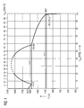
- the chrome-copper state diagram shows 100% chrome on the left side and 100% copper on the right side.
- the chromium is known to have a comparatively high Melting point, namely 1550 ° C.
- copper has a comparatively low melting point, namely 1083 ° C.
- a eutectic is formed at a copper content of 98.2.
- Below the melting point of copper there is a narrow range of solubility for chromium. Otherwise, in the solid state below 700 ° C copper and chromium are not soluble in each other.
- the state diagram chromium-copper furthermore exhibits the peculiarity of a miscibility gap in the liquid state, whereby a monotectic is formed: above the monotectic temperature of 1470 ° C., the range is between about 6% copper and 58% copper up to a temperature of about 2000 ° C two different CuCr melts, which are not miscible with each other.
- the latter means that first of all a homogeneous melt of more than 2000 ° C. has to be produced, which is then cooled rapidly in order to obtain the "homogeneous state"("freeze”). This can, for example, by arc remelting according to the EP 0 115 292 B1 be achieved.
- FIG. 2 A microstructure of a copper-chromium material produced by the arc remelting process is shown in FIG. 2 shown. Specifically, in FIG. 2 Reference numeral 21 is a copper matrix in which chromium particles 22 are precipitated. Overall, the predetermined chromium content results in a largely isotropic size and concentration distribution of the chromium particles 22 in the copper matrix 21.
- FIG. 3 an arrangement is shown as it is commonly known for the production of amorphous metal films ("supercooled glasses").
- the reference numeral 31 a rotatable about an axis perpendicular to the paper plane I rotatable copper wheel, 32 a trough with a cooling bath for the copper wheel 31 and 33 a reservoir for a CuCr melt.
- the electric heater and other control means are in FIG. 3 not shown.
- the solidification process in contrast to the process used in the production of metallic glasses, so led that the resulting CuCr layer is not homogeneous over the thickness of the resulting metal strip, but a concentration gradient of the excreted chromium is such that Preferably, the lighter chromium accumulates on the top surface of the belt. This is facilitated by the fact that the underside first solidifies, the upper portion of the resulting strip (sheet) but remains liquid longer and thus migrate the deposited Cr particles by their buoyancy in the heavier liquid copper to the top, where a concentration of chromium takes place.
- a thin strip 50 or a sheet of predetermined thickness thus results with a copper and chromium concentration corresponding to the melt.
- the width of the band 50 is predetermined by the transverse extent of the copper roller 31. With appropriate dimensioning can also produce sheets of greater width.
- the particular advantage of the specified production method is that segregation of the constituents can be predetermined according to their specific weight of the components during the cooling process. This means that the lighter components, in this case the chrome particles or droplets, diffuse to the surface.
- FIG. 4 A microstructure of such a band-shaped contact material is in FIG. 4 shown.
- the grinding is done in the direction perpendicular to the band 50 FIG. 3 ,
- FIG. 4 51 denotes the copper matrix and 52 denotes the chromium particles present therein.
- a now anisotropic concentration distribution of the chromium portion perpendicular to the surface of the strip 50 is recognized. On the surface of the strip 50 results a high chromium concentration and a finely dispersed distribution of the chromium particles. On the underside of the band 50, on the other hand, a low chromium concentration is present.
- the overall thermal conductivity perpendicular to the contact surface is greatly positively influenced, resulting in an improved switching behavior, especially in terms of a higher switching capacity, compared to homogeneous, the prior art corresponding contacts.
- the latter facilitates in particular the connection of the contact pad to contact carriers, which usually consist of copper.
- contact carriers usually consist of copper.
- the chromium content is of particular importance. This is now concentrated on the surface of the contact pads.
- FIG. 5 50 means the alloy band out FIG. 3 , which for example has a thickness of 2 mm.
- disks 60 with, for example, four radial slots 61 to 64 can be punched out with a tool (not shown in detail). It is essential that only a single appropriately trained tool is needed and that in particular a subsequent machining is no longer required. This achieves a further reduction of the manufacturing costs compared to the prior art.
- FIG. 6 A complete vacuum switch contact 100 for use as a radial field or axial field contact in vacuum switching devices is in FIG. 6 shown.
- the vacuum switch contact 100 consists of a contact pin 110 for current conduction and a contact pot 120 with slits 121 to 124 in the pot wall.
- the contact disk 60 On the upper edge of the contact pot 120, the contact disk 60 is made FIG. 5 fixed by brazing in such a way that the slots 61 to 64 connect to the slots 121 to 124 in the wall of the contact pot 120.
- FIG. 6 form the complete contact arrangement for a vacuum switch. Depending on whether the slits in the contact wells in the same direction or against each other, a total of a radial or axially extending to the contact arrangement magnetic field is generated, which has an effect on the switching behavior.
Landscapes
- Engineering & Computer Science (AREA)
- Mechanical Engineering (AREA)
- Chemical & Material Sciences (AREA)
- Materials Engineering (AREA)
- Metallurgy (AREA)
- Organic Chemistry (AREA)
- Contacts (AREA)
- High-Tension Arc-Extinguishing Switches Without Spraying Means (AREA)
- Manufacture Of Switches (AREA)
- Conductive Materials (AREA)
Description
- Die Erfindung bezieht sich auf ein Verfahren zur Herstellung von Kupfer-Chrom-Kontakten für Vakuumschalter.
- Vakuumschaltröhren für die Energieversorgung und -verteilung benötigen elektrische Schaltkontakte aus einem lichtbogenresistenten Werkstoff, welcher den hohen thermischen Belastungen von z. T. über 5 MW/cm2 widersteht, keine gasförmigen oder sonstigen schädlichen Verunreinigungen freisetzt und insbesondere wirtschaftlich gefertigt werden kann.
- Meist werden für Schaltkontakte in Vakuumschaltröhren kupferhaltige Werkstoffe, im überwiegenden Teil eine Mischung aus Kupfer (Cu) und Chrom (Cr), eingesetzt, wobei i. a. der Chromanteil zwischen 20 %-m (Massenprozent) und 50 % (Massenprozent) beträgt. Die speziellen, in der Vakuumschalttechnik eingesetzten Kontaktformen (Knopf- oder Scheibenkontakt, Spiralkontakt, Topfkontakt, oder Axialmagnetfeldkontakt) erfordern, dass der Kontaktbereich mechanisch bearbeitet werden muss, so dass Materialstärken von mindestens 2 bis 3 mm benötigt werden.
- Zur Herstellung von Werkstoffen aus Kupfer (Cu) und Chrom (Cr) ist das Zustandsdiagramm heranzuziehen. Dies ist beispielsweise aus dem Handbuch von M. Hansen und K. Anderko "Constitution of Binary Alloys", McGraw-Hill Book Company, Inc. (1958), Seite 524 bekannt. Das Zustandsdiagramm Cu-Cr weist thermodynamische Besonderheiten, insbesondere ein Eutektikum und ein Monotektikum, auf, auf die weiter unten noch eingegangen wird.
- Da sich die beiden Metalle Kupfer (Cu) und Chrom (Cr) in ihrer Dichte deutlich unterscheiden, ist die direkte Herstellung von homogenen Schmelzwerkstoffen nicht möglich, da sich die schwerere Komponente (Cu) absetzt. Im Allgemeinen werden daher für die hochwertigsten Kontaktwerkstoffe so genannte Umschmelzwerkstoffe eingesetzt.
- Gemäß der
EP 0 115 292 B1 können Umschmelzwerkstoffe dadurch hergestellt werden, dass ein grob vorgesinterter Zylinder aus CuCr mit Hilfe eines elektrischen Lichtbogens in Edelgasatmosphäre nochmals zu einem hochdichten, homogenen, feinkörnigen Werkstoff umgeschmolzen wird. Aus den daraus erhaltenen zylindrischen Rohlingen werden anschließend Scheiben gesägt, die im Folgenden nochmals spanend bearbeitet werden, um geeignete Endkonturen, Schlitze und/oder Oberflächen der Kontakte zu erhalten. Insbesondere die notwendige Beseitigung von Graten, welche beim spanenden Formen erzeugt werden, führt zu hohen Kosten solcherart hergestellter Kontakte. - Durch den hohen Chromanteil ist ein CuCr-Werkstoff nur für die einfachsten Kontaktformen für eine Konturgebung durch Stanzen geeignet. Bei spanender Bearbeitung des harten Materials ist ein hoher Werkzeugverschleiß mit entsprechend hohen Werkzeugkosten unvermeidbar.
- Andere Herstellverfahren für Kupfer-Chrom-Schaltkontakte, wie z. B. die Herstellung von dicht gesinterten Rohlingen in endkonturnaher Form, erfordern im Allgemeinen ebenfalls noch eine spannende Nachbearbeitung mit den oben beschriebenen Nachteilen. Zudem ist bei Sinterwerkstoffen aus fertigungstechnischen Gründen die Korngrößenverteilung zu erheblich größeren Korngrößen verschoben, was ungünstigere Schalt- und Abbrandeigenschaften im Vergleich zu Umschmelzwerkstoffen zur Folge hat.
- Spezifische sintermetallurgisch hergestellte Kupfer-Chrom-Kontaktwerkstoffe sind in der
DE 38 29 250 A1 und derDE 38 42 919 A1 beschrieben. - Für hohe Ansprüche an die Qualität von CuCr-Schaltontakten werden daher weitere Prozessschritte zur Kornverfeinerung im oberflächennahen Bereich in Betracht gezogen. Beispielsweise bietet sich ein Umschmelzen durch Einsatz von Laser oder Lichtbögen an.
- Die
US 4 780 582 offenbart einen Schaltkontakt aus Kupfer und Chrom für Vakuumschalter. Ferner sei noch auf dieJP 10-287939 - Von obigem Stand der Technik ausgehend ist es Aufgabe der Erfindung, ein vereinfachtes Herstellungsverfahren für Kupfer-Chrom-Kontakte anzugeben.
- Die Aufgabe ist erfindungsgemäß durch ein Herstellungsverfahren gemäß Patentanspruch 1 gelöst. Weiterbildungen des erfindungsgemäßen Herstellungsverfahrens sind in den abhängigen Ansprüchen angegeben.
- Das erfindungsgemäße Verfahren beruht auf der Verarbeitung einer Schmelze aus CuCr durch rasche Erstarrung zu dünnen, typischerweise 1 bis 2 mm dicken Bändern bzw. Blechen, wobei sich durch die Abkühlrate der Schmelze ein Cr-Konzentrationsprofil senkrecht zur Blechoberfläche gezielt einstellen lässt. Dabei wird Gebrauch von der Technologie der Herstellung amorpher Metalle, bei der durch schnelle Erstarrung das Metall in ein thermodynamisches Nichtgleichgewicht überführt wird, gemacht. Solche amorphe Metalle werden auch als Metallgläser bezeichnet.
- Die Technologie der Rascherstarrung von Metallen ist vom Stand der Technik hinreichend bekannt, wozu auf die
DE 694 18 938 T2 , dieDE 35 28 891 C2 und dieDE 36 17 608 C2 verwiesen wird. Mit solchen Methoden werden so genannte amorphe Metalle mit feinsten Ausscheidungen von hochschmelzenden Komponenten hergestellt, wobei solche Komponenten beispielsweise Chrom sein können. Nicht bekannt für die Rascherstarrungstechnik ist allerdings das System Kupfer-Chrom mit Kupfer als Matrix und Chrom als hochschmelzender Komponente. - Bei der Erfindung reichert sich vorteilhafterweise aufgrund des Dichteunterschiedes das Chrom (Cr) auf natürliche Weise an der Oberfläche an und das entstehende Dichteprofil wird beim Erstarren "eingefroren".
- Durch Ausstanzen mit entsprechend geformten Stanzwerkzeugen erhält man die gewünschte Kontaktform. Eine Nachbearbeitung der Schaltkontakte ist vorteilhafterweise nur im Bereich der Verbindungsstellen zu den Kontaktträgern, d.h. im Lotbereich, notwendig, um die hier notwendigen Toleranzen und Oberflächenqualitäten zu erzeugen.
- Die so hergestellten, kostengünstigen Stanzkontakte können als Kontaktauflagen mit kontakttragenden Strukturen verbunden werden, z. B. durch Hartlötung, um die benötigte mechanische Festigkeit zu erzielen.
- Alternativ können auch dickere Bleche von mehreren mm Dicke mit der beschriebenen Methode hergestellt werden, bei denen nur in einigen 1/10 mm in Oberflächennähe Cr feinstdispers vorhanden ist. Durch die größere Materialstärke, die durch den kostengünstigen Rohstoff Kupfer direkt erzeugt werden kann, kann dabei in nur einem einzelnen Arbeitsschritt ein auch mechanisch belastbares Kontaktstück erzeugt werden, wobei wegen der günstigen Werkstoffeigenschaften von Kupfer ebenfalls Stanztechnik zur Formgebung eingesetzt werden kann. Dies führt zu besonders kostengünstigen Kontaktscheiben für Vakuumschaltkontakte.
- Die wesentlichen Vorteile des beschriebenen Verfahrens liegen zum einen in der Materialeinsparung durch den Wegfall spanender Bearbeitung (Sägen, Drehen, Fräsen) sowie durch gezielte Einstellung der aus elektrotechnischen Gründen notwendigen Materialstärke. Zum anderen erzielt man eine größere Wirtschaftlichkeit durch einen deutlich verringerten Chrom-Bedarf, da die teure Komponente Chrom nur noch im Kontaktoberflächenbereich eingesetzt wird. Weiterhin folgen aus dem Stanzprozess kürzere Fertigungszeiten und geringere Betriebskosten, da das Stanzen anstelle von Drehen, Fräsen leichter automatisierbar ist.
- Als entscheidenden Vorteil der Erfindung auf der elektrotechnischen Seite erhält man ein erheblich verbessertes Schaltverhalten zum einen durch die natürliche Einstellung einer feinkörnigen Struktur nahe der Oberfläche, zum anderen aber auch durch die verbesserte Wärmeleitung durch den positiven Cu-Gradienten zur Kontaktunterseite hin.
- Weitere Einzelheiten und Vorteile der Erfindung ergeben sich aus der nachfolgenden Beschreibung von Ausführungsbeispielen. Dabei wird insbesondere auf die Zeichnung gemäß Anlage verwiesen.
- Es zeigen
- Figur 1
- das Zustandsdiagramm von Chrom (Cr) - Kupfer (Cu) und
- Figur 2
- ein Gefügebild eines Kupfer-Chrom-Werkstoffes mit 20 % Chromanteil (CuCr20),
- Figur 3
- eine Vorrichtung zur Herstellung von dünnen Werks- stoffbändern nach Art der Herstellung von amorphen Metallen,
- Figur 4
- ein Gefügebild im Schnitt durch ein mit einer Ein- richtung gemäß
Figur 3 hergestelltes Cu-Cr-Band, - Figur 5
- die Draufsicht auf ein Legierungsband mit daraus aus- gestanzten Kontaktschreiben und
- Figur 6
- einen Vakuumschalterkontakt mit geschlitztem Kontakt- topf und einer Kontaktscheibe gemäß
Figur 5 . - In
Figur 1 ist das Zustandsdiagramm Chrom-Kupfer in der Weise dargestellt, dass 100 % Chromgehalt an der linken Seite und 100 % Kupfergehalt auf der rechten Seite aufgetragen sind. Das Chrom hat bekanntermaßen einen vergleichsweise hohen Schmelzpunkt und zwar 1550°C. Kupfer hat demgegenüber einen vergleichsweise niedrigen Schmelzpunkt, und zwar 1083°C. Bei einer Temperatur von 1075° wird bei einem Kupfergehalt von 98,2 ein Eutektikum gebildet. Unterhalb des Schmelzpunktes von Kupfer existiert ein schmaler Löslichkeitsbereich für Chrom. Ansonsten sind im festen Zustand unterhalb von 700°C Kupfer und Chrom nicht ineinander löslich. - Das Zustandsdiagramm Chrom-Kupfer weist weiterhin die Besonderheit einer Mischungslücke im flüssigen Zustand auf, wobei ein Monotektikum gebildet wird: Oberhalb der monotektischen Temperatur von 1470°C liegen im Bereich zwischen etwa 6 % Kupfer und 58 % Kupfer bis zu einer Temperatur von ca. 2000°C zwei unterschiedliche CuCr-Schmelzen vor, die nicht miteinander mischbar sind.
- Für die praktische Herstellung von im festen Zustand homogenen Kupfer-Chrom-Werkstoffen bedeutet letzteres, dass zunächst eine homogene Schmelze von mehr als 2000°C hergestellt werden muss, die dann schnell abgekühlt wird, um den homogenen Zustand zu erhalten ("einzufrieren"). Dies kann beispielsweise durch Lichtbogen-Umschmelzen gemäß der
EP 0 115 292 B1 erreicht werden. - Ein Gefüge eines Kupfer-Chrom-Werkstoffes, das mit dem Lichtbogen-Umschmelzverfahren erzeugt wurde, ist in
Figur 2 dargestellt. Im Einzelnen bedeutet inFigur 2 das Bezugzeichen 21 eine Kupfer-Matrix, in der Chromteilchen 22 ausgeschieden sind. Insgesamt ergibt sich bei dem vorgegebenen Chromanteil eine weitestgehend isotrope Größen- und Konzentrationsverteilung der Chromteilchen 22 in der Kupfermatrix 21. - In der
Figur 3 ist eine Anordnung dargestellt, wie sie üblicherweise zur Herstellung von amorphen Metallfilmen ("unterkühlte Gläser") bekannt ist. Im Einzelnen bedeuten inFigur 2 das Bezugzeichen 31 ein um eine senkrecht zur Papierebene stehende Achse I drehbares Kupferrad, 32 eine Wanne mit einem Kühlungsbad für das Kupferrad 31 und 33 einen Vorratsbehälter für eine CuCr-Schmelze. Die elektrische Heizeinrichtung und andere regelungstechnische Mittel sind inFigur 3 nicht dargestellt. - Durch Aufsprühen der homogenen Schmelze mit Temperaturen T > 2000°C aus dem Vorratsbehälter 33 auf das sich drehende Rad 31, d.h. auf die sich drehende walze, wird auf dessen Oberfläche CuCr-Material gleicher Zusammensetzung abgeschieden, wobei durch Kühlung und Erstarrung der Schmelze mit definierter Abkühlrate dT/dt sich spezifische Parameter vorgeben lassen.
- Insbesondere wird bei optimaler Abkühlrate der Erstarrungsprozess, im Gegensatz zu der bei der Herstellung metallischer Gläser verwendeten Prozessführung, so geführt, dass die entstehende CuCr-Schicht nicht homogen über die Dicke des entstehenden Metallbandes ist, sondern sich ein Konzentrationsgefälle des ausgeschiedenen Chroms dergestalt ergibt, dass sich das leichtere Chrom bevorzugt an der oberen Oberfläche des Bandes ansammelt. Dies wird dadurch erleichtert, dass die Unterseite zuerst erstarrt, der obere Bereich des entstehenden Bandes (Blechs) aber länger flüssig bleibt und somit die abgeschiedenen Cr-Teilchen durch Ihren Auftrieb im schwereren flüssigen Kupfer an die Oberseite wandern, wo eine Aufkonzentration des Chroms stattfindet.
- In Abhängigkeit von der Umfangsgeschwindigkeit des Kupferrades 31 entsteht somit ein dünnes Band 50 bzw. ein Blech vorgegebener Dicke mit einer der Schmelze entsprechenden Kupfer- und Chromkonzentration. Die Breite des Bandes 50 ist durch die Querausdehnung der Kupferwalze 31 vorgegeben. Bei entsprechender Dimensionierung lassen sich auch Bleche größerer Breite erzeugen.
- Aus dem so hergestellten Band 50 bzw. Blech lassen sich nahezu beliebige Kontaktformen ausstanzen, welche mittels bekannter Mittel auf vorgegebene Kontaktträger aufbringbar sind, beispielsweise durch Hartlöten.
- Durch die spezifischen Randbedingungen der Abkühlung der Schmelze auf dem Kupferrad 31 lässt sich erreichen, dass im CuCr-Band 50 senkrecht zur Bandrichtung eine anisotrope Chrom-Konzentrationsverteilung vorliegt.
- Der besondere Vorteil des angegebenen Herstellungsverfahrens besteht darin, dass sich beim Abkühlvorgang eine Segregation der Bestandteile nach ihrem spezifischen Gewicht der Komponenten vorgeben lässt. Dies bedeutet, dass die leichteren Bestandteile, im vorliegenden Fall die Chrompartikel bzw. Tröpfchen, an die Oberfläche diffundieren.
- Ein Gefügebild eines solchen bandförmigen Kontaktmaterials ist in
Figur 4 dargestellt. Dabei erfolgt der Schliff in senkrechter Richtung zum Band 50 ausFigur 3 . - Im Einzelnen sind in
Figur 4 mit 51 die Kupfermatrix bezeichnet und mit 52 die darin vorhandenen Chromteilchen. Man erkennt eine nunmehr anisotrope Konzentrationsverteilung des Chromanteils senkrecht zur Oberfläche des Bandes 50. An der Oberfläche des Bandes 50 ergibt sich eine hohe Chrom-Konzentration und eine feindisperse Verteilung der Chrom-Teilchen. An der Unterseite des Bandes 50 liegt dagegen eine niedrige Chrom-Konzentration vor. Dadurch wird insgesamt die Wärmeleitfähigkeit senkrecht zur Kontaktoberfläche stark positiv beeinflusst, woraus sich ein verbessertes Schaltverhalten, insbesondere im Sinne eines höheren Schaltvermögens, gegenüber homogenen, dem Stand der Technik entsprechenden Kontakten ergibt. - Letzteres erleichtert insbesondere die Verbindung der Kontaktauflage auf Kontaktträgern, welche üblicherweise aus Kupfer bestehen. Für die bestimmungsgemäße Verwendung von Kupfer-Chrom-Kontakten bei Vakuumschaltern ist dabei der Chromanteil von besonderer Bedeutung. Dieser ist nunmehr an der Oberfläche der Kontaktauflagen konzentriert.
- Insgesamt ergeben sich somit beachtliche Vorteile für die Abbrandfestigkeit und andere Schalteigenschaften der Schaltkontakte von Vakuumschaltern. Insbesondere wird bei dieser Methode der Herstellung das für die Schalteigenschaften notwendige Chrom nur noch in dem Bereich bereitgestellt, in dem es physikalisch bedingt benötigt wird, nämlich in dem dem Kontaktspalt zugewandten Oberflächenbereich der Kontakte. Dadurch kann, neben der erreichbaren höheren Feinkörnigkeit des Chroms, mit erheblich geringeren Chromgesamtmengen gearbeitet werden, was deutliche Kostenvorteile gegenüber herkömmlichen Herstellverfahren ergibt.
- In der Draufsicht gemäß
Figur 5 bedeutet 50 das Legierungsband ausFigur 3 , das beispielsweise eine Dicke von 2 mm hat. Aus dem Band 50 können mit einem nicht im Einzelnen dargestellten Werkzeug Scheiben 60 mit beispielsweise vier Radialschlitzen 61 bis 64 ausgestanzt werden. Wesentlich ist dabei, dass nur ein einziges entsprechend ausgebildetes Werkzeug benötigt wird und dass insbesondere eine nachfolgende spanende Bearbeitung nicht mehr erforderlich ist. Dadurch wird eine weitere Senkung der Herstellkosten gegenüber dem Stand der Technik erzielt. - Ein kompletter Vakuumschalterkontakt 100 zur Verwendung als Radialfeld- oder Axialfeldkontakt in Vakuumschaltgeräten ist in
Figur 6 dargestellt. Der Vakuumschalterkontakt 100 besteht aus einem Kontaktbolzen 110 zur Stromführung und einem Kontakttopf 120 mit Schlitzungen 121 bis 124 in der Topfwandung. Auf dem oberen Rand des Kontakttopfes 120 ist die Kontaktscheibe 60 ausFigur 5 durch Hartlöten befestigt und zwar derart, dass die Schlitze 61 bis 64 an die Schlitzungen 121 bis 124 in der Wandung des Kontakttopfes 120 anschließen. - Durch die Schlitzungen 121 bis 124 im Kontakttopf 120 wird der Strom in den zwischen den Schlitzungen 12 bis 124 gebildeten Bereichen geführt. Dabei entsteht ein Magnetfeld, das den beim Schalten gebildeten Lichtbogen beeinflusst. Jeweils zwei Topfkontakte entsprechend
Figur 6 bilden die komplette Kontaktanordnung für einen Vakuumschalter. Je nachdem ob die Schlitzungen in den Kontakttöpfen in die gleiche Richtung oder gegeneinander verlaufen, wird insgesamt ein radiales oder ein axial zur Kontaktanordnung verlaufendes Magnetfeld generiert, welches sich auf das Schaltverhalten auswirkt. - Es können somit kostengünstig Vakuumschalterkontakte mit alternativ radialem oder axialem Magnetfeld hergestellt werden. Der senkrecht zur Schaltfläche gerichtete Konzentrationsgradient des Chroms sorgt für einen minimierten Kontaktabbrand bei optimalem Schaltverhalten.
Claims (7)
- Verfahren zur Herstellung von Kontakten aus Kupfer (Cu) und Chrom (Cr) als Schaltkontakte für Vakuumschalter, wobei aus einem CuCr-Schmelzwerkstoff durch schnelles Abkühlen auf Raumtemperatur eine vorgegebene Chrom-Konzentration im nichtthermodynamischen Gleichgewicht eingestellt wird,
mit folgenden Verfahrensschritten:- als Ausgangsmaterial für die Schaltkontakte wird ein Band bzw. ein dünnes Blech aus Kupfer (Cu) und Chrom (Cr) mittels eines Gießverfahrens mit rascher Abkühlung erzeugt, wobei- zur Herstellung des Bandes bzw. Bleches flüssiges Kupfer-Chrom vorgegebener Konzentration mit hoher Temperatur auf eine drehende Walze gespritzt oder gegossen wird, wobei der Walze Kühlmittel zugeordnet sind, so dass die flüssige Metalllegierung abgekühlt wird,- aus dem Band bzw. Blech wird eine Kontaktauflage ausgestanzt und- das Stanzteil wird auf einem Kontaktträger befestigt. - Herstellungsverfahren nach Anspruch 1, dadurch gekennzeichnet, dass das Band bzw. Blech eine Stärke von 1 bis 2 mm hat.
- Herstellungsverfahren nach Anspruch 1 oder 2, dadurch gekennzeichnet, dass die Abkühlrate definiert eingestellt wird.
- Herstellungsverfahren nach einem der vorhergehenden Ansprüche, dadurch gekennzeichnet, dass durch die definiert eingestellte Abkühlrate ein vorgegebenes Chrom-Konzentrationsprofil senkrecht zur Band-/Blechoberfläche gezielt eingestellt wird.
- Herstellungsverfahren nach Anspruch 4, dadurch gekennzeichnet, dass aufgrund des Dichteunterschiedes von Chrom und Kupfer sich Chrom an der Oberfläche des Bandes bzw. Bleches anreichert.
- Herstellungsverfahren nach Anspruch 1, dadurch gekennzeichnet, dass die Befestigung des Stanzteils auf dem Kontaktträger durch Hartlöten erfolgt.
- Herstellungsverfahren nach Anspruch 1, dadurch gekennzeichnet, dass durch das Stanzteil eine Kontaktauflage auf dem Kontaktträger gebildet wird.
Applications Claiming Priority (2)
| Application Number | Priority Date | Filing Date | Title |
|---|---|---|---|
| DE102006021772A DE102006021772B4 (de) | 2006-05-10 | 2006-05-10 | Verfahren zur Herstellung von Kupfer-Chrom-Kontakten für Vakuumschalter und zugehörige Schaltkontakte |
| PCT/EP2007/054453 WO2007128819A2 (de) | 2006-05-10 | 2007-05-08 | Verfahren zur herstellung von kupfer-chrom-kontakten für vakuumschalter und zugehörige schaltkontakte |
Publications (2)
| Publication Number | Publication Date |
|---|---|
| EP2018445A2 EP2018445A2 (de) | 2009-01-28 |
| EP2018445B1 true EP2018445B1 (de) | 2010-09-22 |
Family
ID=38579926
Family Applications (1)
| Application Number | Title | Priority Date | Filing Date |
|---|---|---|---|
| EP07728906A Not-in-force EP2018445B1 (de) | 2006-05-10 | 2007-05-08 | Verfahren zur herstellung von kupfer-chrom-kontakten für vakuumschalter |
Country Status (5)
| Country | Link |
|---|---|
| EP (1) | EP2018445B1 (de) |
| CN (1) | CN101460640B (de) |
| AT (1) | ATE482295T1 (de) |
| DE (2) | DE102006021772B4 (de) |
| WO (1) | WO2007128819A2 (de) |
Families Citing this family (5)
| Publication number | Priority date | Publication date | Assignee | Title |
|---|---|---|---|---|
| AT11814U1 (de) | 2010-08-03 | 2011-05-15 | Plansee Powertech Ag | Verfahren zum pulvermetallurgischen herstellen eines cu-cr-werkstoffs |
| CN112683057B (zh) * | 2020-12-25 | 2021-09-14 | 东北大学 | 一种用于制备固态电解质材料的多模块真空设备 |
| CN113084129B (zh) * | 2021-04-09 | 2022-04-01 | 江苏瑞德磁性材料有限公司 | 一种金属薄膜的制备装置及制备方法 |
| CN116574937B (zh) * | 2023-05-08 | 2023-10-03 | 江苏爱斯凯电气有限公司 | 一种用作真空开关的触头材料及其制备方法 |
| CN118989353B (zh) * | 2024-10-25 | 2025-04-08 | 陕西斯瑞新材料股份有限公司 | 基于slm对混粉烧结铜铬触头表面致密度改性的方法及铜铬触头 |
Family Cites Families (13)
| Publication number | Priority date | Publication date | Assignee | Title |
|---|---|---|---|---|
| DE2509406C3 (de) * | 1975-03-04 | 1979-02-22 | Standard Elektrik Lorenz Ag, 7000 Stuttgart | Verfahren zur automatischen Herstellung einer elektrischen Widerstandsschweißverbindung zwischen einem aus einem Metallband herausgestanzten Kontakt und einem Kontaktträger sowie Vorrichtung zur Durchführung des Verfahrens |
| US4221257A (en) * | 1978-10-10 | 1980-09-09 | Allied Chemical Corporation | Continuous casting method for metallic amorphous strips |
| DE3303170A1 (de) * | 1983-01-31 | 1984-08-02 | Siemens AG, 1000 Berlin und 8000 München | Verfahren zum herstellen von kupfer-chrom-schmelzlegierungen als kontaktwerkstoff fuer vakuum-leistungsschalter |
| EP0172411B1 (de) * | 1984-07-30 | 1988-10-26 | Siemens Aktiengesellschaft | Vakuumschütz mit Kontaktstücken aus CuCr und Verfahren zur Herstellung dieser Kontaktstücke |
| JPS6149753A (ja) * | 1984-08-13 | 1986-03-11 | Nippon Steel Corp | 金属薄帯および線の製造方法 |
| CH671534A5 (de) * | 1986-03-14 | 1989-09-15 | Escher Wyss Ag | |
| DE3829250A1 (de) * | 1988-08-29 | 1990-03-01 | Siemens Ag | Verfahren zur herstellung eines kontaktwerkstoffes fuer vakuumschalter |
| DE3938234A1 (de) * | 1988-11-19 | 1990-05-31 | Glyco Metall Werke | Verfahren und vorrichtung zur herstellung eines schichtwerkstoffes fuer gleitelemente |
| DE3842919C2 (de) * | 1988-12-21 | 1995-04-27 | Calor Emag Elektrizitaets Ag | Schaltstück für einen Vakuumschalter |
| DE4003018A1 (de) * | 1990-02-02 | 1991-08-08 | Metallgesellschaft Ag | Verfahren zur herstellung monotektischer legierungen |
| GB2274656B (en) * | 1993-01-29 | 1996-12-11 | London Scandinavian Metall | Alloying additive |
| JPH10287939A (ja) * | 1997-04-17 | 1998-10-27 | Furukawa Electric Co Ltd:The | 打抜加工性に優れた電気電子機器用銅合金 |
| CN1264143A (zh) * | 2000-02-24 | 2000-08-23 | 周武平 | 真空开关铜铬系触头材料的制造方法 |
-
2006
- 2006-05-10 DE DE102006021772A patent/DE102006021772B4/de not_active Expired - Fee Related
-
2007
- 2007-05-08 DE DE502007005146T patent/DE502007005146D1/de active Active
- 2007-05-08 AT AT07728906T patent/ATE482295T1/de active
- 2007-05-08 WO PCT/EP2007/054453 patent/WO2007128819A2/de not_active Ceased
- 2007-05-08 EP EP07728906A patent/EP2018445B1/de not_active Not-in-force
- 2007-05-08 CN CN200780016675.3A patent/CN101460640B/zh not_active Expired - Fee Related
Also Published As
| Publication number | Publication date |
|---|---|
| ATE482295T1 (de) | 2010-10-15 |
| DE102006021772B4 (de) | 2009-02-05 |
| DE102006021772A1 (de) | 2007-11-15 |
| DE502007005146D1 (de) | 2010-11-04 |
| CN101460640A (zh) | 2009-06-17 |
| EP2018445A2 (de) | 2009-01-28 |
| WO2007128819A2 (de) | 2007-11-15 |
| CN101460640B (zh) | 2015-05-20 |
| WO2007128819A3 (de) | 2008-11-20 |
Similar Documents
| Publication | Publication Date | Title |
|---|---|---|
| EP0115292B1 (de) | Verfahren zum Herstellen von Kupfer-Chrom-Schmelzlegierungen als Kontaktwerkstoff für Vakuum-Leistungsschalter | |
| EP2600996B1 (de) | Verfahren zum pulvermetallurgischen herstellen eines cu-cr-werkstoffs | |
| EP3247530B1 (de) | Hartlotlegierung | |
| EP2018445B1 (de) | Verfahren zur herstellung von kupfer-chrom-kontakten für vakuumschalter | |
| EP1307311A1 (de) | Verfahren zur herstellung präziser bauteile mittels lasersintern | |
| EP0440620B1 (de) | Halbzeug für elektrische kontakte aus einem verbundwerkstoff auf silber-zinnoxid-basis und pulvermetallurgisches verfahren zu seiner herstellung | |
| WO2014202390A1 (de) | Verfahren und vorrichtung zur herstellung von kontaktelementen für elektrische schaltkontakte | |
| DE3406535C2 (de) | ||
| DE102008056264A1 (de) | Verfahren zur Herstellung eines Halbzeugs und Halbzeug für elektrische Kontakte sowie Kontaktstück | |
| EP0172411B1 (de) | Vakuumschütz mit Kontaktstücken aus CuCr und Verfahren zur Herstellung dieser Kontaktstücke | |
| DE10010723B4 (de) | Verfahren zum Herstellen eines Kontaktwerkstoff-Halbzeuges für Kontaktstücke für Vakuumschaltgeräte sowie Kontaktwerkstoff-Halbzeuge und Kontaktstücke für Vakuumschaltgeräte | |
| DE69825227T2 (de) | Vakuumschalter | |
| WO2013030123A1 (de) | Verfahren zur herstellung eines halbzeugs für elektrische kontakte sowie kontaktstück | |
| EP2524384B1 (de) | Elektrisches kontaktelement und verfahren zur herstellung eines elektrischen kontaktelements | |
| DE10392662T5 (de) | Kupfer-Nickel-Silizium Zwei-Phasen Abschrecksubstrat | |
| DE112017001814T5 (de) | Kontaktelement, verfahren zur herstellung desselben und vakuum-schaltungsunterbrecher | |
| DE19928330C2 (de) | Verwendung einer zinnreichen Kupfer-Zinn-Eisen-Knetlegierung | |
| DE19902499C2 (de) | Verfahren zum Herstellen einer Kontaktanordnung für eine Vakuumschaltröhre | |
| DE112004001542T5 (de) | Kupfer-Nickel-Silizium Zweiphasen-Abschrecksubstrat | |
| DD208701B1 (de) | Verfahren zur herstellung von schaltstuecken | |
| DD209317A1 (de) | Kontaktwerkstoff fuer vakuumschalter und verfahren zur herstellung | |
| EP1848019B1 (de) | Verfahren zur Herstellung eines Kontaktstückes, sowie Kontaktstück für Nieder-, Mittel,- Hochspannungs- und Generatorschaltgeräte | |
| DE19841582A1 (de) | Verwendung einer Kupfer-Chrom-Legierung | |
| WO2017134068A1 (de) | Kontaktelement für elektrische schalter und herstellungsverfahren dazu |
Legal Events
| Date | Code | Title | Description |
|---|---|---|---|
| PUAI | Public reference made under article 153(3) epc to a published international application that has entered the european phase |
Free format text: ORIGINAL CODE: 0009012 |
|
| 17P | Request for examination filed |
Effective date: 20081009 |
|
| AK | Designated contracting states |
Kind code of ref document: A2 Designated state(s): AT BE BG CH CY CZ DE DK EE ES FI FR GB GR HU IE IS IT LI LT LU LV MC MT NL PL PT RO SE SI SK TR |
|
| AX | Request for extension of the european patent |
Extension state: AL BA HR MK RS |
|
| 17Q | First examination report despatched |
Effective date: 20090310 |
|
| DAX | Request for extension of the european patent (deleted) | ||
| GRAP | Despatch of communication of intention to grant a patent |
Free format text: ORIGINAL CODE: EPIDOSNIGR1 |
|
| RTI1 | Title (correction) |
Free format text: METHOD FOR THE PRODUCTION OF COPPER-CHROMIUM CONTACTS FOR VACUUM SWITCHES |
|
| GRAS | Grant fee paid |
Free format text: ORIGINAL CODE: EPIDOSNIGR3 |
|
| GRAA | (expected) grant |
Free format text: ORIGINAL CODE: 0009210 |
|
| AK | Designated contracting states |
Kind code of ref document: B1 Designated state(s): AT BE BG CH CY CZ DE DK EE ES FI FR GB GR HU IE IS IT LI LT LU LV MC MT NL PL PT RO SE SI SK TR |
|
| REG | Reference to a national code |
Ref country code: GB Ref legal event code: FG4D Free format text: NOT ENGLISH |
|
| REG | Reference to a national code |
Ref country code: CH Ref legal event code: EP |
|
| REG | Reference to a national code |
Ref country code: IE Ref legal event code: FG4D Free format text: LANGUAGE OF EP DOCUMENT: GERMAN |
|
| REF | Corresponds to: |
Ref document number: 502007005146 Country of ref document: DE Date of ref document: 20101104 Kind code of ref document: P |
|
| PG25 | Lapsed in a contracting state [announced via postgrant information from national office to epo] |
Ref country code: LT Free format text: LAPSE BECAUSE OF FAILURE TO SUBMIT A TRANSLATION OF THE DESCRIPTION OR TO PAY THE FEE WITHIN THE PRESCRIBED TIME-LIMIT Effective date: 20100922 Ref country code: FI Free format text: LAPSE BECAUSE OF FAILURE TO SUBMIT A TRANSLATION OF THE DESCRIPTION OR TO PAY THE FEE WITHIN THE PRESCRIBED TIME-LIMIT Effective date: 20100922 |
|
| REG | Reference to a national code |
Ref country code: NL Ref legal event code: VDEP Effective date: 20100922 |
|
| LTIE | Lt: invalidation of european patent or patent extension |
Effective date: 20100922 |
|
| PG25 | Lapsed in a contracting state [announced via postgrant information from national office to epo] |
Ref country code: SI Free format text: LAPSE BECAUSE OF FAILURE TO SUBMIT A TRANSLATION OF THE DESCRIPTION OR TO PAY THE FEE WITHIN THE PRESCRIBED TIME-LIMIT Effective date: 20100922 Ref country code: PL Free format text: LAPSE BECAUSE OF FAILURE TO SUBMIT A TRANSLATION OF THE DESCRIPTION OR TO PAY THE FEE WITHIN THE PRESCRIBED TIME-LIMIT Effective date: 20100922 |
|
| PG25 | Lapsed in a contracting state [announced via postgrant information from national office to epo] |
Ref country code: SE Free format text: LAPSE BECAUSE OF FAILURE TO SUBMIT A TRANSLATION OF THE DESCRIPTION OR TO PAY THE FEE WITHIN THE PRESCRIBED TIME-LIMIT Effective date: 20100922 Ref country code: GR Free format text: LAPSE BECAUSE OF FAILURE TO SUBMIT A TRANSLATION OF THE DESCRIPTION OR TO PAY THE FEE WITHIN THE PRESCRIBED TIME-LIMIT Effective date: 20101223 Ref country code: LV Free format text: LAPSE BECAUSE OF FAILURE TO SUBMIT A TRANSLATION OF THE DESCRIPTION OR TO PAY THE FEE WITHIN THE PRESCRIBED TIME-LIMIT Effective date: 20100922 |
|
| REG | Reference to a national code |
Ref country code: IE Ref legal event code: FD4D |
|
| PG25 | Lapsed in a contracting state [announced via postgrant information from national office to epo] |
Ref country code: IE Free format text: LAPSE BECAUSE OF FAILURE TO SUBMIT A TRANSLATION OF THE DESCRIPTION OR TO PAY THE FEE WITHIN THE PRESCRIBED TIME-LIMIT Effective date: 20100922 |
|
| PG25 | Lapsed in a contracting state [announced via postgrant information from national office to epo] |
Ref country code: RO Free format text: LAPSE BECAUSE OF FAILURE TO SUBMIT A TRANSLATION OF THE DESCRIPTION OR TO PAY THE FEE WITHIN THE PRESCRIBED TIME-LIMIT Effective date: 20100922 Ref country code: NL Free format text: LAPSE BECAUSE OF FAILURE TO SUBMIT A TRANSLATION OF THE DESCRIPTION OR TO PAY THE FEE WITHIN THE PRESCRIBED TIME-LIMIT Effective date: 20100922 Ref country code: PT Free format text: LAPSE BECAUSE OF FAILURE TO SUBMIT A TRANSLATION OF THE DESCRIPTION OR TO PAY THE FEE WITHIN THE PRESCRIBED TIME-LIMIT Effective date: 20110124 Ref country code: IS Free format text: LAPSE BECAUSE OF FAILURE TO SUBMIT A TRANSLATION OF THE DESCRIPTION OR TO PAY THE FEE WITHIN THE PRESCRIBED TIME-LIMIT Effective date: 20110122 Ref country code: IT Free format text: LAPSE BECAUSE OF FAILURE TO SUBMIT A TRANSLATION OF THE DESCRIPTION OR TO PAY THE FEE WITHIN THE PRESCRIBED TIME-LIMIT Effective date: 20100922 Ref country code: CZ Free format text: LAPSE BECAUSE OF FAILURE TO SUBMIT A TRANSLATION OF THE DESCRIPTION OR TO PAY THE FEE WITHIN THE PRESCRIBED TIME-LIMIT Effective date: 20100922 Ref country code: SK Free format text: LAPSE BECAUSE OF FAILURE TO SUBMIT A TRANSLATION OF THE DESCRIPTION OR TO PAY THE FEE WITHIN THE PRESCRIBED TIME-LIMIT Effective date: 20100922 Ref country code: EE Free format text: LAPSE BECAUSE OF FAILURE TO SUBMIT A TRANSLATION OF THE DESCRIPTION OR TO PAY THE FEE WITHIN THE PRESCRIBED TIME-LIMIT Effective date: 20100922 |
|
| PG25 | Lapsed in a contracting state [announced via postgrant information from national office to epo] |
Ref country code: ES Free format text: LAPSE BECAUSE OF FAILURE TO SUBMIT A TRANSLATION OF THE DESCRIPTION OR TO PAY THE FEE WITHIN THE PRESCRIBED TIME-LIMIT Effective date: 20110102 |
|
| PLBE | No opposition filed within time limit |
Free format text: ORIGINAL CODE: 0009261 |
|
| STAA | Information on the status of an ep patent application or granted ep patent |
Free format text: STATUS: NO OPPOSITION FILED WITHIN TIME LIMIT |
|
| 26N | No opposition filed |
Effective date: 20110623 |
|
| PG25 | Lapsed in a contracting state [announced via postgrant information from national office to epo] |
Ref country code: DK Free format text: LAPSE BECAUSE OF FAILURE TO SUBMIT A TRANSLATION OF THE DESCRIPTION OR TO PAY THE FEE WITHIN THE PRESCRIBED TIME-LIMIT Effective date: 20100922 |
|
| REG | Reference to a national code |
Ref country code: DE Ref legal event code: R097 Ref document number: 502007005146 Country of ref document: DE Effective date: 20110623 |
|
| BERE | Be: lapsed |
Owner name: SIEMENS A.G. Effective date: 20110531 |
|
| PG25 | Lapsed in a contracting state [announced via postgrant information from national office to epo] |
Ref country code: MT Free format text: LAPSE BECAUSE OF FAILURE TO SUBMIT A TRANSLATION OF THE DESCRIPTION OR TO PAY THE FEE WITHIN THE PRESCRIBED TIME-LIMIT Effective date: 20100922 Ref country code: MC Free format text: LAPSE BECAUSE OF NON-PAYMENT OF DUE FEES Effective date: 20110531 |
|
| REG | Reference to a national code |
Ref country code: CH Ref legal event code: PL |
|
| GBPC | Gb: european patent ceased through non-payment of renewal fee |
Effective date: 20110508 |
|
| PG25 | Lapsed in a contracting state [announced via postgrant information from national office to epo] |
Ref country code: LI Free format text: LAPSE BECAUSE OF NON-PAYMENT OF DUE FEES Effective date: 20110531 Ref country code: CH Free format text: LAPSE BECAUSE OF NON-PAYMENT OF DUE FEES Effective date: 20110531 |
|
| PG25 | Lapsed in a contracting state [announced via postgrant information from national office to epo] |
Ref country code: BE Free format text: LAPSE BECAUSE OF NON-PAYMENT OF DUE FEES Effective date: 20110531 |
|
| PG25 | Lapsed in a contracting state [announced via postgrant information from national office to epo] |
Ref country code: GB Free format text: LAPSE BECAUSE OF NON-PAYMENT OF DUE FEES Effective date: 20110508 |
|
| PG25 | Lapsed in a contracting state [announced via postgrant information from national office to epo] |
Ref country code: CY Free format text: LAPSE BECAUSE OF FAILURE TO SUBMIT A TRANSLATION OF THE DESCRIPTION OR TO PAY THE FEE WITHIN THE PRESCRIBED TIME-LIMIT Effective date: 20100922 Ref country code: LU Free format text: LAPSE BECAUSE OF NON-PAYMENT OF DUE FEES Effective date: 20110508 |
|
| REG | Reference to a national code |
Ref country code: AT Ref legal event code: MM01 Ref document number: 482295 Country of ref document: AT Kind code of ref document: T Effective date: 20120508 |
|
| PG25 | Lapsed in a contracting state [announced via postgrant information from national office to epo] |
Ref country code: AT Free format text: LAPSE BECAUSE OF NON-PAYMENT OF DUE FEES Effective date: 20120508 |
|
| PG25 | Lapsed in a contracting state [announced via postgrant information from national office to epo] |
Ref country code: TR Free format text: LAPSE BECAUSE OF FAILURE TO SUBMIT A TRANSLATION OF THE DESCRIPTION OR TO PAY THE FEE WITHIN THE PRESCRIBED TIME-LIMIT Effective date: 20100922 Ref country code: BG Free format text: LAPSE BECAUSE OF FAILURE TO SUBMIT A TRANSLATION OF THE DESCRIPTION OR TO PAY THE FEE WITHIN THE PRESCRIBED TIME-LIMIT Effective date: 20101222 |
|
| PG25 | Lapsed in a contracting state [announced via postgrant information from national office to epo] |
Ref country code: HU Free format text: LAPSE BECAUSE OF FAILURE TO SUBMIT A TRANSLATION OF THE DESCRIPTION OR TO PAY THE FEE WITHIN THE PRESCRIBED TIME-LIMIT Effective date: 20100922 |
|
| REG | Reference to a national code |
Ref country code: FR Ref legal event code: PLFP Year of fee payment: 10 |
|
| REG | Reference to a national code |
Ref country code: FR Ref legal event code: PLFP Year of fee payment: 11 |
|
| REG | Reference to a national code |
Ref country code: FR Ref legal event code: PLFP Year of fee payment: 12 |
|
| PGFP | Annual fee paid to national office [announced via postgrant information from national office to epo] |
Ref country code: FR Payment date: 20210526 Year of fee payment: 15 |
|
| PGFP | Annual fee paid to national office [announced via postgrant information from national office to epo] |
Ref country code: DE Payment date: 20210720 Year of fee payment: 15 |
|
| REG | Reference to a national code |
Ref country code: DE Ref legal event code: R119 Ref document number: 502007005146 Country of ref document: DE |
|
| PG25 | Lapsed in a contracting state [announced via postgrant information from national office to epo] |
Ref country code: FR Free format text: LAPSE BECAUSE OF NON-PAYMENT OF DUE FEES Effective date: 20220531 |
|
| PG25 | Lapsed in a contracting state [announced via postgrant information from national office to epo] |
Ref country code: DE Free format text: LAPSE BECAUSE OF NON-PAYMENT OF DUE FEES Effective date: 20221201 |