EP2006414A2 - Atomic layer growing apparatus - Google Patents
Atomic layer growing apparatus Download PDFInfo
- Publication number
- EP2006414A2 EP2006414A2 EP07740060A EP07740060A EP2006414A2 EP 2006414 A2 EP2006414 A2 EP 2006414A2 EP 07740060 A EP07740060 A EP 07740060A EP 07740060 A EP07740060 A EP 07740060A EP 2006414 A2 EP2006414 A2 EP 2006414A2
- Authority
- EP
- European Patent Office
- Prior art keywords
- source gas
- supply
- valve
- buffer tank
- film forming
- Prior art date
- Legal status (The legal status is an assumption and is not a legal conclusion. Google has not performed a legal analysis and makes no representation as to the accuracy of the status listed.)
- Withdrawn
Links
- 239000000463 material Substances 0.000 claims abstract description 56
- 238000002347 injection Methods 0.000 claims abstract description 41
- 239000007924 injection Substances 0.000 claims abstract description 41
- 230000008016 vaporization Effects 0.000 claims description 11
- 239000006200 vaporizer Substances 0.000 abstract description 16
- 239000000758 substrate Substances 0.000 abstract description 15
- 238000010438 heat treatment Methods 0.000 abstract description 6
- 238000001947 vapour-phase growth Methods 0.000 abstract description 3
- 239000007789 gas Substances 0.000 description 156
- 238000000034 method Methods 0.000 description 69
- 239000010408 film Substances 0.000 description 54
- 238000010926 purge Methods 0.000 description 31
- 238000000231 atomic layer deposition Methods 0.000 description 18
- 239000010409 thin film Substances 0.000 description 6
- 125000002524 organometallic group Chemical group 0.000 description 5
- 238000000151 deposition Methods 0.000 description 4
- 238000010586 diagram Methods 0.000 description 4
- XKRFYHLGVUSROY-UHFFFAOYSA-N Argon Chemical compound [Ar] XKRFYHLGVUSROY-UHFFFAOYSA-N 0.000 description 2
- IJGRMHOSHXDMSA-UHFFFAOYSA-N Atomic nitrogen Chemical compound N#N IJGRMHOSHXDMSA-UHFFFAOYSA-N 0.000 description 2
- 230000015572 biosynthetic process Effects 0.000 description 2
- 230000008021 deposition Effects 0.000 description 2
- 230000000694 effects Effects 0.000 description 2
- 239000007791 liquid phase Substances 0.000 description 2
- 229910044991 metal oxide Inorganic materials 0.000 description 2
- 150000004706 metal oxides Chemical class 0.000 description 2
- 230000001590 oxidative effect Effects 0.000 description 2
- 239000004065 semiconductor Substances 0.000 description 2
- CBENFWSGALASAD-UHFFFAOYSA-N Ozone Chemical compound [O-][O+]=O CBENFWSGALASAD-UHFFFAOYSA-N 0.000 description 1
- 229910052786 argon Inorganic materials 0.000 description 1
- QVGXLLKOCUKJST-UHFFFAOYSA-N atomic oxygen Chemical compound [O] QVGXLLKOCUKJST-UHFFFAOYSA-N 0.000 description 1
- 150000001875 compounds Chemical class 0.000 description 1
- 239000013078 crystal Substances 0.000 description 1
- 239000011521 glass Substances 0.000 description 1
- 239000011261 inert gas Substances 0.000 description 1
- 238000005259 measurement Methods 0.000 description 1
- 229910052757 nitrogen Inorganic materials 0.000 description 1
- 239000001301 oxygen Substances 0.000 description 1
- 229910052760 oxygen Inorganic materials 0.000 description 1
- 238000004904 shortening Methods 0.000 description 1
- FZHAPNGMFPVSLP-UHFFFAOYSA-N silanamine Chemical compound [SiH3]N FZHAPNGMFPVSLP-UHFFFAOYSA-N 0.000 description 1
- 239000000243 solution Substances 0.000 description 1
- 230000001629 suppression Effects 0.000 description 1
- 239000011364 vaporized material Substances 0.000 description 1
Images


Classifications
-
- C—CHEMISTRY; METALLURGY
- C23—COATING METALLIC MATERIAL; COATING MATERIAL WITH METALLIC MATERIAL; CHEMICAL SURFACE TREATMENT; DIFFUSION TREATMENT OF METALLIC MATERIAL; COATING BY VACUUM EVAPORATION, BY SPUTTERING, BY ION IMPLANTATION OR BY CHEMICAL VAPOUR DEPOSITION, IN GENERAL; INHIBITING CORROSION OF METALLIC MATERIAL OR INCRUSTATION IN GENERAL
- C23C—COATING METALLIC MATERIAL; COATING MATERIAL WITH METALLIC MATERIAL; SURFACE TREATMENT OF METALLIC MATERIAL BY DIFFUSION INTO THE SURFACE, BY CHEMICAL CONVERSION OR SUBSTITUTION; COATING BY VACUUM EVAPORATION, BY SPUTTERING, BY ION IMPLANTATION OR BY CHEMICAL VAPOUR DEPOSITION, IN GENERAL
- C23C16/00—Chemical coating by decomposition of gaseous compounds, without leaving reaction products of surface material in the coating, i.e. chemical vapour deposition [CVD] processes
- C23C16/44—Chemical coating by decomposition of gaseous compounds, without leaving reaction products of surface material in the coating, i.e. chemical vapour deposition [CVD] processes characterised by the method of coating
- C23C16/455—Chemical coating by decomposition of gaseous compounds, without leaving reaction products of surface material in the coating, i.e. chemical vapour deposition [CVD] processes characterised by the method of coating characterised by the method used for introducing gases into reaction chamber or for modifying gas flows in reaction chamber
-
- C—CHEMISTRY; METALLURGY
- C23—COATING METALLIC MATERIAL; COATING MATERIAL WITH METALLIC MATERIAL; CHEMICAL SURFACE TREATMENT; DIFFUSION TREATMENT OF METALLIC MATERIAL; COATING BY VACUUM EVAPORATION, BY SPUTTERING, BY ION IMPLANTATION OR BY CHEMICAL VAPOUR DEPOSITION, IN GENERAL; INHIBITING CORROSION OF METALLIC MATERIAL OR INCRUSTATION IN GENERAL
- C23C—COATING METALLIC MATERIAL; COATING MATERIAL WITH METALLIC MATERIAL; SURFACE TREATMENT OF METALLIC MATERIAL BY DIFFUSION INTO THE SURFACE, BY CHEMICAL CONVERSION OR SUBSTITUTION; COATING BY VACUUM EVAPORATION, BY SPUTTERING, BY ION IMPLANTATION OR BY CHEMICAL VAPOUR DEPOSITION, IN GENERAL
- C23C16/00—Chemical coating by decomposition of gaseous compounds, without leaving reaction products of surface material in the coating, i.e. chemical vapour deposition [CVD] processes
- C23C16/44—Chemical coating by decomposition of gaseous compounds, without leaving reaction products of surface material in the coating, i.e. chemical vapour deposition [CVD] processes characterised by the method of coating
- C23C16/455—Chemical coating by decomposition of gaseous compounds, without leaving reaction products of surface material in the coating, i.e. chemical vapour deposition [CVD] processes characterised by the method of coating characterised by the method used for introducing gases into reaction chamber or for modifying gas flows in reaction chamber
- C23C16/45523—Pulsed gas flow or change of composition over time
- C23C16/45525—Atomic layer deposition [ALD]
- C23C16/45544—Atomic layer deposition [ALD] characterized by the apparatus
-
- C—CHEMISTRY; METALLURGY
- C23—COATING METALLIC MATERIAL; COATING MATERIAL WITH METALLIC MATERIAL; CHEMICAL SURFACE TREATMENT; DIFFUSION TREATMENT OF METALLIC MATERIAL; COATING BY VACUUM EVAPORATION, BY SPUTTERING, BY ION IMPLANTATION OR BY CHEMICAL VAPOUR DEPOSITION, IN GENERAL; INHIBITING CORROSION OF METALLIC MATERIAL OR INCRUSTATION IN GENERAL
- C23C—COATING METALLIC MATERIAL; COATING MATERIAL WITH METALLIC MATERIAL; SURFACE TREATMENT OF METALLIC MATERIAL BY DIFFUSION INTO THE SURFACE, BY CHEMICAL CONVERSION OR SUBSTITUTION; COATING BY VACUUM EVAPORATION, BY SPUTTERING, BY ION IMPLANTATION OR BY CHEMICAL VAPOUR DEPOSITION, IN GENERAL
- C23C16/00—Chemical coating by decomposition of gaseous compounds, without leaving reaction products of surface material in the coating, i.e. chemical vapour deposition [CVD] processes
-
- C—CHEMISTRY; METALLURGY
- C23—COATING METALLIC MATERIAL; COATING MATERIAL WITH METALLIC MATERIAL; CHEMICAL SURFACE TREATMENT; DIFFUSION TREATMENT OF METALLIC MATERIAL; COATING BY VACUUM EVAPORATION, BY SPUTTERING, BY ION IMPLANTATION OR BY CHEMICAL VAPOUR DEPOSITION, IN GENERAL; INHIBITING CORROSION OF METALLIC MATERIAL OR INCRUSTATION IN GENERAL
- C23C—COATING METALLIC MATERIAL; COATING MATERIAL WITH METALLIC MATERIAL; SURFACE TREATMENT OF METALLIC MATERIAL BY DIFFUSION INTO THE SURFACE, BY CHEMICAL CONVERSION OR SUBSTITUTION; COATING BY VACUUM EVAPORATION, BY SPUTTERING, BY ION IMPLANTATION OR BY CHEMICAL VAPOUR DEPOSITION, IN GENERAL
- C23C16/00—Chemical coating by decomposition of gaseous compounds, without leaving reaction products of surface material in the coating, i.e. chemical vapour deposition [CVD] processes
- C23C16/44—Chemical coating by decomposition of gaseous compounds, without leaving reaction products of surface material in the coating, i.e. chemical vapour deposition [CVD] processes characterised by the method of coating
- C23C16/448—Chemical coating by decomposition of gaseous compounds, without leaving reaction products of surface material in the coating, i.e. chemical vapour deposition [CVD] processes characterised by the method of coating characterised by the method used for generating reactive gas streams, e.g. by evaporation or sublimation of precursor materials
-
- C—CHEMISTRY; METALLURGY
- C23—COATING METALLIC MATERIAL; COATING MATERIAL WITH METALLIC MATERIAL; CHEMICAL SURFACE TREATMENT; DIFFUSION TREATMENT OF METALLIC MATERIAL; COATING BY VACUUM EVAPORATION, BY SPUTTERING, BY ION IMPLANTATION OR BY CHEMICAL VAPOUR DEPOSITION, IN GENERAL; INHIBITING CORROSION OF METALLIC MATERIAL OR INCRUSTATION IN GENERAL
- C23C—COATING METALLIC MATERIAL; COATING MATERIAL WITH METALLIC MATERIAL; SURFACE TREATMENT OF METALLIC MATERIAL BY DIFFUSION INTO THE SURFACE, BY CHEMICAL CONVERSION OR SUBSTITUTION; COATING BY VACUUM EVAPORATION, BY SPUTTERING, BY ION IMPLANTATION OR BY CHEMICAL VAPOUR DEPOSITION, IN GENERAL
- C23C16/00—Chemical coating by decomposition of gaseous compounds, without leaving reaction products of surface material in the coating, i.e. chemical vapour deposition [CVD] processes
- C23C16/44—Chemical coating by decomposition of gaseous compounds, without leaving reaction products of surface material in the coating, i.e. chemical vapour deposition [CVD] processes characterised by the method of coating
- C23C16/448—Chemical coating by decomposition of gaseous compounds, without leaving reaction products of surface material in the coating, i.e. chemical vapour deposition [CVD] processes characterised by the method of coating characterised by the method used for generating reactive gas streams, e.g. by evaporation or sublimation of precursor materials
- C23C16/4485—Chemical coating by decomposition of gaseous compounds, without leaving reaction products of surface material in the coating, i.e. chemical vapour deposition [CVD] processes characterised by the method of coating characterised by the method used for generating reactive gas streams, e.g. by evaporation or sublimation of precursor materials by evaporation without using carrier gas in contact with the source material
Definitions
- the present invention relates to an atomic layer growing apparatus which can form a thin film by depositing atomic layers and molecular layers one after another and, more particularly, to an atomic layer growing apparatus which can supply a source gas while the pressure, for example, is stable.
- atomic layer deposition is used as a technique of forming a uniform thin film on a substrate having a large area with a good reproducibility
- pattern reference 1 Japanese Patent Laid-Open No. 05-186295 .
- the atomic layer deposition is a technique of forming a thin film by depositing atomic layers one after another by alternately supplying materials of respective elements composing a film to be formed.
- one or n layers alone are adsorbed onto the substrate surface while supplying the materials of the respective elements so that no surplus materials contribute to the deposition. This is called the self-limiting deposition. Since the atomic layer deposition uses no plasma, it can form a high-quality film.
- the processing temperature need only be set as low as, e.g., about 300°C in the atomic layer deposition, an insulating film can be formed even on a glass substrate.
- the atomic layer deposition has a feature that it can be applied widely.
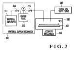
- An atomic layer growing apparatus to practice the atomic layer deposition having the above-described feature includes a film forming chamber 301 in which the vapor phase growth of a film is performed, a substrate table 302 having a heating mechanism accommodated in the film forming chamber 301, and an exhaust mechanism 304, as shown in Fig. 3 .
- the atomic layer growing apparatus also includes a material supply mechanism 305 including a source gas vaporizer 351 and buffer tank 352, and a purge gas supply unit 307.
- a substrate 303 to be processed is loaded onto the substrate table 302, and the film forming chamber 301 is sealed.
- the supply of a predetermined gas by the material supply mechanism 305, the evacuation of the chamber 301 by the exhaust mechanism 304, the purge of the surplus gas by supplying a purge gas by the purge gas supply unit 307, and the evacuation of the chamber 301 by the exhaust mechanism 304 are repeated, thereby forming a desired thin film.
- a material (organometallic material) used in the formation of an insulating film by the atomic layer growing apparatus is in the liquid phase at an atmospheric pressure of about 20°C.
- the material supply mechanism 305 vaporizes the material in the liquid phase by the source gas vaporizer 351, and supplies the vaporized material into the film forming chamber 301.
- the material supply mechanism 305 supplies a source gas into the film forming chamber 301 while a variation in pressure, for example, is suppressed by using the buffer tank 352.
- a supply valve 354 of the film forming chamber 301 is opened while a fill valve 353 of the buffer tank 352 is closed. This control can suppress a variation in pressure caused when the source gas from the source gas vaporizer 351 flows directly.
- the buffer tank 352 is filled with a source gas generated by the source gas vaporizer 351 while the supply valve 354 is closed and the fill valve 353 is open.
- the fill valve 353 is closed and the supply valve 354 is opened to supply the source gas by the buffer tank 352. Therefore, the source gas cannot be supplied into the film forming chamber 301 while the buffer tank 352 is filled with the source gas. Note that when the buffer tank 352 is filled with the source gas while the supply of the source gas is stopped in each cycle of the atomic layer deposition, it is possible to stably supply the source gas into the film forming chamber 301 at a given stage as needed.
- the conventional apparatus shown in Fig. 3 often cannot stably supply the source gas when each cycle of the atomic layer deposition is shortened.
- the present invention has been made to solve the above-described problem, and has as its object to make it possible to stably supply the source gas even when the source gas supply process in the atomic layer deposition is shortened.
- An atomic layer growing apparatus comprises at least a film forming chamber having an internal space which can be sealed, material vaporizing means for generating a source gas by vaporizing a material, a plurality of buffer tanks filled with a source gas generated by the material vaporizing means, fill valves which are respectively attached to the buffer tanks and control the filling of the source gas generated by the material vaporizing means, supply valves which respectively control the supply of a source gas from the buffer tanks, and control means for controlling opening/closing of the fill valves and the supply valves, wherein the control means performs control so that while the source gas is supplied into the film forming chamber by opening the supply valve of at least one of the buffer tanks, other buffer tanks the supply valves of which are not open are filled with a source gas by opening the fill valves of the other tanks.
- This apparatus can always supply the source gas into the film forming chamber while the source vaporizing means and the film forming chamber never communicate with each other.
- control means may control to supply the source gas into the film forming chamber by closing a supply valve of the buffer tank filled with a source gas by opening a fill valve of the buffer tank, and by opening a supply valve of a buffer tank filled with the source gas in excess of a prescribed lower limit.
- the above-described atomic layer growing apparatus may further comprise an injection control valve which controls injection of a source gas supplied from the buffer tanks into the film forming chamber, wherein the control means performs control so that while the source gas is supplied into the film forming chamber by opening the injection control valve and the supply valve of at least one of the buffer tanks, other buffer tanks the supply valves of which are not open are filled with a source gas by opening the fill valves of the other buffer tanks.
- the control means preferably controls to open the injection control valve while a supply valve of a buffer tank filled with a source gas by opening a fill valve of the buffer tank is closed, and a supply valve of a buffer tank filled with a source gas in excess of a prescribed lower limit is open.
- the pressure of the source gas which fills the buffer tank which supplies the source gas into the film forming chamber always exceeds the prescribed lower limit of its internal pressure while the source vaporizing means and the film forming chamber never communicate with each other.
- a plurality of buffer tanks are used so that, for example, the injection control valve is opened while the supply valve of a buffer tank filled with the source gas by opening its fill valve is closed, and the supply valve of a buffer tank filled with the source gas in excess of the prescribed lower limit of its internal pressure is open. That is, a plurality of buffer tanks are used so that while the source gas is supplied into the film forming chamber by opening the supply valve of at least one buffer tank, other buffer tanks the supply valves of which are not open are filled with the source gas by opening the fill valves of the other buffer tanks. This produces an excellent effect of more stably supplying the source gas into the film forming chamber even when the time for the source gas supply process in the atomic layer growth is shortened.
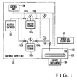
- Fig. 1 is a block diagram showing an example of the arrangement of an atomic layer growing apparatus according to the embodiment of the present invention.
- the atomic layer growing apparatus according to this embodiment shown in Fig. 1 includes a film forming chamber 101 in which the vapor phase growth of a film is performed, a substrate table 102 having a heating mechanism accommodated in the film forming chamber 101, and an exhaust mechanism 104.
- the film forming chamber 101 has an internal space which can be sealed, and accommodates the substrate table 102 in it.
- the atomic layer growing apparatus also includes a material supply unit 105 including a material vaporizer 151, two buffer banks, i.e., a buffer bank A 152a and buffer bank B 152b, a fill valve A 153a and supply valve A 154a of the buffer tank A 152a, a fill valve B 153b and supply valve B 154b of the buffer tank B 152b, an injection control valve 155, and a control unit 156 which controls the opening/closing of each valve.
- the atomic layer growing apparatus according to this embodiment also includes a purge gas supply unit 107 which supplies a purge gas formed from an inert gas such as argon or nitrogen into the film forming chamber 101.
- the material vaporizer 151 accommodates an organometallic material such as aminosilane, and vaporizes the accommodated organometallic material by heating to generate a source gas.
- the source gas generated in this way fills the buffer tank A 152a and buffer tank B 152b first. After that, the source gas which fills the buffer tank A 152a and that which fills the buffer tank B 152b are alternately supplied into the film forming chamber 101.
- the filling of the source gas into the buffer tanks, and the supply of the source gas from the buffer tanks are controlled by controlling the opening/closing of the fill valve A 153a, supply valve A 154a, fill valve B 153b, supply valve B 154b, and injection control valve 155 by the control unit 156.
- the control unit 156 keeps all of the fill valve A 153a, supply valve A 154a, fill valve B 153b, supply valve B 154b, and injection control valve 155 closed.
- the control unit 156 opens the supply valve A 154a and injection control valve 155 to supply the source gas from the buffer tank A 152a into the film forming chamber 101.
- the control unit 156 opens the fill valve B 153b to fill the buffer tank B 152b with the source gas.
- the control unit 156 closes the injection control valve 155.
- the control unit 156 opens the injection control valve 155.
- the control unit 156 closes the fill valve B 153b.
- the control unit 156 closes the supply valve A 154a and opens the fill valve A 153a and supply valve B 154b. With this operation, the source gas is supplied from the buffer tank B 152b into the film forming chamber 101.
- the control unit 156 closes the injection control valve 155.
- the control unit 156 opens the injection control valve 155.
- the control unit 156 closes the fill valve A 153a.
- the control unit 156 closes the injection control valve 155.
- the pressure of the source gas in the buffer tank B 152b becomes lower than its prescribed lower limit, so the control unit 156 closes the supply valve B 154b and opens the fill valve B 153b and supply valve A 154a.
- the control unit 156 opens the injection control valve 155. With this operation, the source gas is supplied from the buffer tank A 152a into the film forming chamber 101. When time t7 at which the source gas supply process ends and the purge process starts comes, the control unit 156 closes the injection control valve 155.
- the control unit 156 opens the injection control valve 155.
- the pressure of the source gas in the buffer tank A 152a becomes lower than its prescribed lower limit, so the control unit 156 closes the supply valve A 154a and opens the fill valve A 153a and supply valve B 154b. With this operation, the source gas is supplied from the buffer tank B 152b into the film forming chamber 101.
- the control unit 156 closes the injection control valve 155.
- the control unit 156 opens the injection control valve 155.
- the control unit 156 closes the fill valve A 153a.
- the control unit 156 closes the injection control valve 155. Also at time t11, the pressure of the source gas in the buffer tank B 152b becomes lower than its prescribed lower limit, so the control unit 156 closes the supply valve B 154b and opens the fill valve B 153b and supply valve A 154a.
- the control unit 156 opens the injection control valve 155. With this operation, the source gas is supplied from the buffer tank A 152a into the film forming chamber 101. Note that the pressure of the source gas described above need only be measured by a manometer P built in each buffer tank.
- a substrate 103 to be processed is loaded onto the substrate table 102, and the film forming chamber 101 is sealed. After that, while the substrate 103 is heated to a predetermined temperature by the heating mechanism of the substrate table 102, the above-described source gas supply process and the above-described purge process including the supply of the purge gas by the purge gas supply unit 107 and the evacuation of the chamber 101 by the exhaust mechanism 104 are repeated, thereby forming a desired thin film.
- the atomic layer growing apparatus uses two buffer tanks so that the source gas is supplied into the film forming chamber by opening the supply valve of one buffer tank, and the other buffer tank is filled with the source gas by opening the fill valve of the other buffer tank.
- this apparatus uses two buffer tanks so that the injection control valve is opened while the supply valve of a buffer tank filled with the source gas by opening its fill valve is closed, and the supply valve of a buffer tank filled with the source gas in excess of the prescribed lower limit of its internal pressure is open. The opening/closing of each valve is controlled by the control unit (control means).
- the material vaporizer 151 and film forming chamber 101 never communicate with each other in all the states. This suppresses a variation in pressure caused when the source gas from the material vaporizer 151 flows directly. Also, the pressure of the source gas which fills a buffer tank which supplies the source gas into the film forming chamber 101 can always exceed its prescribed lower limit. For this reason, even when the atomic layer deposition is performed at a cycle shorter than the time for which one buffer tank is filled with the source gas, the source gas is always supplied into the film forming chamber 101 in the source gas supply process, as shown in the timing chart of Fig. 2 . Also, the source gas is supplied into the film forming chamber 101 always at a stable pressure.
- the use of two buffer tanks allows suppression of wasting of the capacity of the material vaporizer 151 to generate a source gas.
- one buffer tank supplies the source gas
- the filling of the source gas is stopped while the source gas is supplied.
- the generation capacity of the material vaporizer 151 is wasted during the material supply process, which accounts for half the overall process.
- the time for which the filling of the source gas is stopped becomes shorter than the time for the material supply process, as indicated by "Filling State" shown in Fig. 2 . This suppresses wasting of the capacity of the material vaporizer 151 to generate a source gas.
- the supply valve of the other buffer tank is opened to supply the source gas up to the injection control valve 155.
- the injection control valve 155 is closed and the supply valve A 154a is opened at time t5.
- the present invention is not particularly limited to this, and the injection control valve 155 and supply valve A 154a may be opened at time t6. Note that a variation in pressure in the source gas supply can be further suppressed by performing the control shown in Fig. 2 by taking account of a delay of the source gas supply due to the presence of the capacity of the pipe from the supply valve to the injection control valve 155.
- the supply valve of this buffer tank is closed and its fill valve is opened, and the supply valve of the other buffer tank is opened at the same time.
- the pressure in the buffer tank A 152a becomes lower than its prescribed lower limit while the injection control valve 155 is open, so the supply valve A 154a is closed and the fill valve A 153a and supply valve B 154b are opened at the same time.
- the present invention is not particularly limited to this, and the two supply valves may be alternately opened/closed at the timing at which the injection control valve opens. For example, first, at time t0, the injection control valve 155 and supply valve A 154a are opened at the same time. Next, at time t2 at which the injection control valve 155 is opened, the supply valve A 154a is closed and the supply valve B 154b is opened at the same time. Lastly, at time t4 at which the injection control valve 155 is opened, the supply valve B 154b is closed and the supply valve A 154a is opened at the same time. Control is performed to repeat these operations. The fill valve A 153a and fill valve B 153b are controlled to open when the corresponding supply valve A 154a and supply valve B 154b are closed, and they are controlled to close when the pressures in the corresponding buffer tanks reach their specific upper limits.
- the source gas may be supplied into the film forming chamber by controlling the supply valve attached to each buffer tank without using the injection control valve.
- the control of each valve need only be performed as shown in the timing chart of Fig. 4 .
- This control will be explained.
- the injection control valve 155 is opened at all the stages (times).
- the buffer tank A 152a is filled with the source gas.
- the control unit 156 closes the fill valve A 153a, supply valve A 154a, fill valve B 153b, and supply valve B 154b.
- the control unit 156 opens the supply valve A 154a to supply the source gas from the buffer tank A 152a into the film forming chamber 101.
- the control unit 156 closes the supply valve A 154a to stop the source gas supply, and opens the fill valve A 153a to fill the buffer tank A 152a with the source gas.
- the control unit 156 opens the supply valve B 154b to supply the source gas from the buffer tank B 152b into the film forming chamber 101.
- the control unit 156 closes the fill valve A 153a.
- the control unit 156 closes the supply valve B 154b to stop the source gas supply, and opens the fill valve B 153b to fill the buffer tank B 152b with the source gas.
- the control unit 156 opens the supply valve A 154a to supply the source gas from the buffer tank A 152a into the film forming chamber 101.
- the control unit 156 closes the fill valve B 153b.
- the control unit 156 closes the supply valve A 154a to stop the source gas supply, and opens the fill valve A 153a to fill the buffer tank A 152a with the source gas.
- the control unit 156 opens the supply valve B 154b to supply the source gas from the buffer tank B 152b into the film forming chamber 101.
- the control unit 156 closes the fill valve A 153a.
- the control unit 156 closes the supply valve B 154b to stop the source gas supply, and opens the fill valve B 153b to fill the buffer tank B 152b with the source gas. After that, the above-described operation is repeated at times t8, t8', t9, t10, t10', t11, t12, t12',.... Note that the pressure of the source gas described above need only be measured by the manometer P built in each buffer bank.
- the material vaporizer 151 and film forming chamber 101 never communicate with each other. This suppresses a variation in pressure caused when the source gas from the material vaporizer 151 flows directly. Also even in this control, the period from time t1 to time t2' is taken for the filling, and the atomic layer deposition (source gas supply) is performed at a period (cycle) shorter than that period. Nevertheless, the source gas is always supplied into the film forming chamber 101 in the source gas supply process, as shown in the timing chart of Fig. 4 . Also, the source gas is supplied into the film forming chamber 101 always at a stable pressure.
- the present invention is not particularly limited to this.
- the flow rate of the source gas supplied from each supply valve may be measured by a flowmeter F, and the opening/closing of the supply valve of each buffer tank may be controlled on the basis of the measurement result of the flow rate, e.g., by confirming whether the flow rate measured exceeds a predetermined value.
- each buffer tank used need only include a fill valve which controls the filling of a source gas generated by a material vaporizer (material vaporizing means), and a supply valve which controls the supply of the source gas from the buffer tank.
- control need only be performed so that the injection control valve is opened while the supply valve of a buffer tank which fills the source gas by closing its fill valve is closed, and the supply valve of a buffer tank filled with the source gas in excess of the prescribed lower limit of its internal pressure is open.
- the atomic layer growing apparatus according to this embodiment shown in Fig. 1 is also applicable to atomic layer deposition which forms a metal oxide film using an oxidizing gas such as oxygen or ozone, in addition to that which uses a source gas containing an organometallic material.
- an oxidizing gas such as oxygen or ozone
- repeating organometallic source gas supply process ⁇ purge process ⁇ oxidizing gas supply process ⁇ purge process ⁇ ... makes it possible to form a metal oxide film. Even in this case, supplying, in turn, a source gas using a plurality of buffer tanks allows more stable source gas supply even when the time for the gas supply process is shortened.
- the present invention is preferably adopted in the crystal growth of a thin film made of a semiconductor or compound semiconductor, and the formation of, e.g., an oxide film.
Landscapes
- Chemical & Material Sciences (AREA)
- General Chemical & Material Sciences (AREA)
- Chemical Kinetics & Catalysis (AREA)
- Engineering & Computer Science (AREA)
- Materials Engineering (AREA)
- Mechanical Engineering (AREA)
- Metallurgy (AREA)
- Organic Chemistry (AREA)
- Chemical Vapour Deposition (AREA)
- Crystals, And After-Treatments Of Crystals (AREA)
Abstract
An atomic layer growing apparatus includes a film forming chamber (101) in which the vapor phase growth of a film is performed, a substrate table (102) having a heating mechanism accommodated in the film forming chamber (101), and an exhaust mechanism (104). The atomic layer growing apparatus also includes a material supply unit (105) including a material vaporizer (151), two buffer tanks, i.e., a buffer tank A (152a) and buffer tank B (152b), a fill valve A (153a) and supply valve A (154a) of the buffer tank A (152a), a fill valve B (153b) and supply valve B (154b) of the buffer tank B (152b), an injection control valve (155), and a control unit (156) which controls the opening/closing of each valve.
Description
- The present invention relates to an atomic layer growing apparatus which can form a thin film by depositing atomic layers and molecular layers one after another and, more particularly, to an atomic layer growing apparatus which can supply a source gas while the pressure, for example, is stable.
- In recent years, atomic layer deposition (ALD) is used as a technique of forming a uniform thin film on a substrate having a large area with a good reproducibility (patent reference 1: Japanese Patent Laid-Open No.
05-186295 - An atomic layer growing apparatus to practice the atomic layer deposition having the above-described feature includes a
film forming chamber 301 in which the vapor phase growth of a film is performed, a substrate table 302 having a heating mechanism accommodated in thefilm forming chamber 301, and anexhaust mechanism 304, as shown inFig. 3 . The atomic layer growing apparatus also includes amaterial supply mechanism 305 including asource gas vaporizer 351 andbuffer tank 352, and a purgegas supply unit 307. - In the apparatus shown in
Fig. 3 , asubstrate 303 to be processed is loaded onto the substrate table 302, and thefilm forming chamber 301 is sealed. After that, while thesubstrate 303 is heated to a predetermined temperature by the heating mechanism of the substrate table 302, the supply of a predetermined gas by thematerial supply mechanism 305, the evacuation of thechamber 301 by theexhaust mechanism 304, the purge of the surplus gas by supplying a purge gas by the purgegas supply unit 307, and the evacuation of thechamber 301 by theexhaust mechanism 304 are repeated, thereby forming a desired thin film. - A material (organometallic material) used in the formation of an insulating film by the atomic layer growing apparatus is in the liquid phase at an atmospheric pressure of about 20°C. For this reason, the
material supply mechanism 305 vaporizes the material in the liquid phase by thesource gas vaporizer 351, and supplies the vaporized material into thefilm forming chamber 301. Also, thematerial supply mechanism 305 supplies a source gas into thefilm forming chamber 301 while a variation in pressure, for example, is suppressed by using thebuffer tank 352. At the stage of supplying the source gas into thefilm forming chamber 301, asupply valve 354 of thefilm forming chamber 301 is opened while afill valve 353 of thebuffer tank 352 is closed. This control can suppress a variation in pressure caused when the source gas from thesource gas vaporizer 351 flows directly. - However, amid the prevalence of the execution of the atomic layer deposition at a shorter cycle by shortening the purge time and exhaust time, the above-described prior art cannot make the most of the capacity of the
source gas vaporizer 351 to supply the source gas, as will be described later, so the supply of the source gas often runs short. - In the source gas supply, first, the
buffer tank 352 is filled with a source gas generated by thesource gas vaporizer 351 while thesupply valve 354 is closed and thefill valve 353 is open. Next, thefill valve 353 is closed and thesupply valve 354 is opened to supply the source gas by thebuffer tank 352. Therefore, the source gas cannot be supplied into thefilm forming chamber 301 while thebuffer tank 352 is filled with the source gas. Note that when thebuffer tank 352 is filled with the source gas while the supply of the source gas is stopped in each cycle of the atomic layer deposition, it is possible to stably supply the source gas into thefilm forming chamber 301 at a given stage as needed. - However, as described above, when the atomic layer deposition is performed at a shorter cycle, the time for which the supply of the source gas is stopped is shortened, so the source gas supply process starts at a stage before the
buffer tank 352 is completely filled with the source gas. In this state, the source gas is not always supplied throughout the source gas supply process. In this manner, the conventional apparatus shown inFig. 3 often cannot stably supply the source gas when each cycle of the atomic layer deposition is shortened. - The present invention has been made to solve the above-described problem, and has as its object to make it possible to stably supply the source gas even when the source gas supply process in the atomic layer deposition is shortened.
- An atomic layer growing apparatus according to the present invention comprises at least a film forming chamber having an internal space which can be sealed, material vaporizing means for generating a source gas by vaporizing a material, a plurality of buffer tanks filled with a source gas generated by the material vaporizing means, fill valves which are respectively attached to the buffer tanks and control the filling of the source gas generated by the material vaporizing means, supply valves which respectively control the supply of a source gas from the buffer tanks, and control means for controlling opening/closing of the fill valves and the supply valves, wherein the control means performs control so that while the source gas is supplied into the film forming chamber by opening the supply valve of at least one of the buffer tanks, other buffer tanks the supply valves of which are not open are filled with a source gas by opening the fill valves of the other tanks.
- This apparatus can always supply the source gas into the film forming chamber while the source vaporizing means and the film forming chamber never communicate with each other.
- In the above-described atomic layer growing apparatus, the control means may control to supply the source gas into the film forming chamber by closing a supply valve of the buffer tank filled with a source gas by opening a fill valve of the buffer tank, and by opening a supply valve of a buffer tank filled with the source gas in excess of a prescribed lower limit.
- Also, the above-described atomic layer growing apparatus may further comprise an injection control valve which controls injection of a source gas supplied from the buffer tanks into the film forming chamber, wherein the control means performs control so that while the source gas is supplied into the film forming chamber by opening the injection control valve and the supply valve of at least one of the buffer tanks, other buffer tanks the supply valves of which are not open are filled with a source gas by opening the fill valves of the other buffer tanks. In this case, the control means preferably controls to open the injection control valve while a supply valve of a buffer tank filled with a source gas by opening a fill valve of the buffer tank is closed, and a supply valve of a buffer tank filled with a source gas in excess of a prescribed lower limit is open. In this apparatus, the pressure of the source gas which fills the buffer tank which supplies the source gas into the film forming chamber always exceeds the prescribed lower limit of its internal pressure while the source vaporizing means and the film forming chamber never communicate with each other.
- As has been described above, according to the present invention, a plurality of buffer tanks are used so that, for example, the injection control valve is opened while the supply valve of a buffer tank filled with the source gas by opening its fill valve is closed, and the supply valve of a buffer tank filled with the source gas in excess of the prescribed lower limit of its internal pressure is open. That is, a plurality of buffer tanks are used so that while the source gas is supplied into the film forming chamber by opening the supply valve of at least one buffer tank, other buffer tanks the supply valves of which are not open are filled with the source gas by opening the fill valves of the other buffer tanks. This produces an excellent effect of more stably supplying the source gas into the film forming chamber even when the time for the source gas supply process in the atomic layer growth is shortened.
-
-
Fig. 1 is a block diagram showing an example of the arrangement of an atomic layer growing apparatus according to an embodiment of the present invention; -
Fig. 2 is a timing chart showing an example of the control of each valve by acontrol unit 156 shown inFig. 1 ; -
Fig. 3 is a block diagram showing an example of the arrangement of the conventional atomic layer growing apparatus; and -
Fig. 4 is a timing chart showing another example of the control of each valve by thecontrol unit 156 shown inFig. 1 . - An embodiment of the present invention will be described below with reference to the accompanying drawings.
Fig. 1 is a block diagram showing an example of the arrangement of an atomic layer growing apparatus according to the embodiment of the present invention. First, the atomic layer growing apparatus according to this embodiment shown inFig. 1 includes afilm forming chamber 101 in which the vapor phase growth of a film is performed, a substrate table 102 having a heating mechanism accommodated in thefilm forming chamber 101, and an exhaust mechanism 104. Thefilm forming chamber 101 has an internal space which can be sealed, and accommodates the substrate table 102 in it. The atomic layer growing apparatus also includes amaterial supply unit 105 including amaterial vaporizer 151, two buffer banks, i.e., a buffer bank A 152a andbuffer bank B 152b, a fill valve A 153a andsupply valve A 154a of the buffer tank A 152a, afill valve B 153b andsupply valve B 154b of thebuffer tank B 152b, aninjection control valve 155, and acontrol unit 156 which controls the opening/closing of each valve. The atomic layer growing apparatus according to this embodiment also includes a purgegas supply unit 107 which supplies a purge gas formed from an inert gas such as argon or nitrogen into thefilm forming chamber 101. - The
material vaporizer 151 accommodates an organometallic material such as aminosilane, and vaporizes the accommodated organometallic material by heating to generate a source gas. The source gas generated in this way fills the buffer tank A 152a andbuffer tank B 152b first. After that, the source gas which fills the buffer tank A 152a and that which fills thebuffer tank B 152b are alternately supplied into thefilm forming chamber 101. The filling of the source gas into the buffer tanks, and the supply of the source gas from the buffer tanks are controlled by controlling the opening/closing of thefill valve A 153a,supply valve A 154a,fill valve B 153b,supply valve B 154b, andinjection control valve 155 by thecontrol unit 156. - An example of the control of each valve by the
control unit 156 and an example of the source gas supply operation will be explained below with reference to the block diagram shown inFig. 1 and the timing chart shown inFig. 2 . At the initial stage, thebuffer tank A 152a is filled with the source gas. In this state, thecontrol unit 156 keeps all of thefill valve A 153a,supply valve A 154a,fill valve B 153b,supply valve B 154b, andinjection control valve 155 closed. When the source gas supply process in the atomic layer deposition starts at time t0 in this state, thecontrol unit 156 opens thesupply valve A 154a andinjection control valve 155 to supply the source gas from thebuffer tank A 152a into thefilm forming chamber 101. At the same time, thecontrol unit 156 opens thefill valve B 153b to fill thebuffer tank B 152b with the source gas. - When time t1 at which the source gas supply process ends and the purge process starts comes, the
control unit 156 closes theinjection control valve 155. When time t2 at which the purge process ends and the next material gas supply process starts comes, thecontrol unit 156 opens theinjection control valve 155. Also at time t2, when the pressure of the source gas which fills thebuffer tank B 152b reaches its specific upper limit, thecontrol unit 156 closes thefill valve B 153b. At time t2' in this material gas supply process, the pressure of the source gas in thebuffer tank A 152a becomes lower than its prescribed lower limit, so thecontrol unit 156 closes thesupply valve A 154a and opens thefill valve A 153a andsupply valve B 154b. With this operation, the source gas is supplied from thebuffer tank B 152b into thefilm forming chamber 101. - When time t3 at which the source gas supply process ends and the purge process starts comes, the
control unit 156 closes theinjection control valve 155. When time t4 at which the purge process ends and the next material supply process starts comes, thecontrol unit 156 opens theinjection control valve 155. At time t4' in this source gas supply process, when the pressure of the source gas which fills thebuffer tank A 152a reaches its specific upper limit, thecontrol unit 156 closes thefill valve A 153a. When time t5 at which the source gas supply process ends and the purge process starts comes, thecontrol unit 156 closes theinjection control valve 155. At time t5, the pressure of the source gas in thebuffer tank B 152b becomes lower than its prescribed lower limit, so thecontrol unit 156 closes thesupply valve B 154b and opens thefill valve B 153b andsupply valve A 154a. - When time t6 at which the purge process ends and the next material supply process starts comes, the
control unit 156 opens theinjection control valve 155. With this operation, the source gas is supplied from thebuffer tank A 152a into thefilm forming chamber 101. When time t7 at which the source gas supply process ends and the purge process starts comes, thecontrol unit 156 closes theinjection control valve 155. - When time t8 at which the purge process ends and the next material supply process starts comes, the
control unit 156 opens theinjection control valve 155. At time t8' in this material supply process, the pressure of the source gas in thebuffer tank A 152a becomes lower than its prescribed lower limit, so thecontrol unit 156 closes thesupply valve A 154a and opens thefill valve A 153a andsupply valve B 154b. With this operation, the source gas is supplied from thebuffer tank B 152b into thefilm forming chamber 101. - When time t9 at which the source gas supply process ends and the purge process starts comes, the
control unit 156 closes theinjection control valve 155. When time t10 at which the purge process ends and the next material supply process starts comes, thecontrol unit 156 opens theinjection control valve 155. At time t10' in this material supply process, when the pressure of the source gas which fills thebuffer tank A 152a reaches its specific upper limit, thecontrol unit 156 closes thefill valve A 153a. - When time t11 at which the source gas supply process ends and the purge process starts comes, the
control unit 156 closes theinjection control valve 155. Also at time t11, the pressure of the source gas in thebuffer tank B 152b becomes lower than its prescribed lower limit, so thecontrol unit 156 closes thesupply valve B 154b and opens thefill valve B 153b andsupply valve A 154a. When time t12 at which the purge process ends and the next material supply process starts comes, thecontrol unit 156 opens theinjection control valve 155. With this operation, the source gas is supplied from thebuffer tank A 152a into thefilm forming chamber 101. Note that the pressure of the source gas described above need only be measured by a manometer P built in each buffer tank. - In the atomic layer growing apparatus according to this embodiment, a
substrate 103 to be processed is loaded onto the substrate table 102, and thefilm forming chamber 101 is sealed. After that, while thesubstrate 103 is heated to a predetermined temperature by the heating mechanism of the substrate table 102, the above-described source gas supply process and the above-described purge process including the supply of the purge gas by the purgegas supply unit 107 and the evacuation of thechamber 101 by the exhaust mechanism 104 are repeated, thereby forming a desired thin film. - As has been described above, the atomic layer growing apparatus according to this embodiment shown in
Fig. 1 uses two buffer tanks so that the source gas is supplied into the film forming chamber by opening the supply valve of one buffer tank, and the other buffer tank is filled with the source gas by opening the fill valve of the other buffer tank. For example, this apparatus uses two buffer tanks so that the injection control valve is opened while the supply valve of a buffer tank filled with the source gas by opening its fill valve is closed, and the supply valve of a buffer tank filled with the source gas in excess of the prescribed lower limit of its internal pressure is open. The opening/closing of each valve is controlled by the control unit (control means). - Consequently, the
material vaporizer 151 andfilm forming chamber 101 never communicate with each other in all the states. This suppresses a variation in pressure caused when the source gas from thematerial vaporizer 151 flows directly. Also, the pressure of the source gas which fills a buffer tank which supplies the source gas into thefilm forming chamber 101 can always exceed its prescribed lower limit. For this reason, even when the atomic layer deposition is performed at a cycle shorter than the time for which one buffer tank is filled with the source gas, the source gas is always supplied into thefilm forming chamber 101 in the source gas supply process, as shown in the timing chart ofFig. 2 . Also, the source gas is supplied into thefilm forming chamber 101 always at a stable pressure. - As described above, the use of two buffer tanks allows suppression of wasting of the capacity of the
material vaporizer 151 to generate a source gas. When one buffer tank supplies the source gas, the filling of the source gas is stopped while the source gas is supplied. Accordingly, in the example shown inFig. 2 , the generation capacity of thematerial vaporizer 151 is wasted during the material supply process, which accounts for half the overall process. In contrast, when two buffer tanks supply the source gas, the time for which the filling of the source gas is stopped becomes shorter than the time for the material supply process, as indicated by "Filling State" shown inFig. 2 . This suppresses wasting of the capacity of thematerial vaporizer 151 to generate a source gas. - The above description has been given assuming that even at the stage where the material supply process is not performed (while the
injection control valve 155 is closed), when the pressure of the source gas in one buffer tank becomes lower than its prescribed lower limit, the supply valve of the other buffer tank is opened to supply the source gas up to theinjection control valve 155. For example, theinjection control valve 155 is closed and thesupply valve A 154a is opened at time t5. However, the present invention is not particularly limited to this, and theinjection control valve 155 andsupply valve A 154a may be opened at time t6. Note that a variation in pressure in the source gas supply can be further suppressed by performing the control shown inFig. 2 by taking account of a delay of the source gas supply due to the presence of the capacity of the pipe from the supply valve to theinjection control valve 155. - Also in the above-described method, when the pressure in a buffer tank becomes lower than its prescribed lower limit while the material supply process is performed (while the
injection control valve 155 is open), the supply valve of this buffer tank is closed and its fill valve is opened, and the supply valve of the other buffer tank is opened at the same time. For example, at time t2', the pressure in thebuffer tank A 152a becomes lower than its prescribed lower limit while theinjection control valve 155 is open, so thesupply valve A 154a is closed and thefill valve A 153a andsupply valve B 154b are opened at the same time. - However, the present invention is not particularly limited to this, and the two supply valves may be alternately opened/closed at the timing at which the injection control valve opens. For example, first, at time t0, the
injection control valve 155 andsupply valve A 154a are opened at the same time. Next, at time t2 at which theinjection control valve 155 is opened, thesupply valve A 154a is closed and thesupply valve B 154b is opened at the same time. Lastly, at time t4 at which theinjection control valve 155 is opened, thesupply valve B 154b is closed and thesupply valve A 154a is opened at the same time. Control is performed to repeat these operations. Thefill valve A 153a and fillvalve B 153b are controlled to open when the correspondingsupply valve A 154a andsupply valve B 154b are closed, and they are controlled to close when the pressures in the corresponding buffer tanks reach their specific upper limits. - The source gas may be supplied into the film forming chamber by controlling the supply valve attached to each buffer tank without using the injection control valve. For example, the control of each valve need only be performed as shown in the timing chart of
Fig. 4 . This control will be explained. In this example, first, theinjection control valve 155 is opened at all the stages (times). At the initial stage, thebuffer tank A 152a is filled with the source gas. In this state, thecontrol unit 156 closes thefill valve A 153a,supply valve A 154a, fillvalve B 153b, andsupply valve B 154b. When the source gas supply process in the atomic layer deposition starts at time t0 in this state, thecontrol unit 156 opens thesupply valve A 154a to supply the source gas from thebuffer tank A 152a into thefilm forming chamber 101. - When time t1 at which the source gas supply process ends and the purge process starts comes, the
control unit 156 closes thesupply valve A 154a to stop the source gas supply, and opens thefill valve A 153a to fill thebuffer tank A 152a with the source gas. When time t2 at which the purge process ends and the next material supply process starts comes, thecontrol unit 156 opens thesupply valve B 154b to supply the source gas from thebuffer tank B 152b into thefilm forming chamber 101. At time t2' in this material supply process, when the pressure of the source gas which fills thebuffer tank A 152a reaches its specific upper limit, thecontrol unit 156 closes thefill valve A 153a. - When time t3 at which the source gas supply process ends and the purge process starts comes, the
control unit 156 closes thesupply valve B 154b to stop the source gas supply, and opens thefill valve B 153b to fill thebuffer tank B 152b with the source gas. When time t4 at which the purge process ends and the next material supply process starts comes, thecontrol unit 156 opens thesupply valve A 154a to supply the source gas from thebuffer tank A 152a into thefilm forming chamber 101. At time t4' in this material supply process, when the pressure of the source gas which fills thebuffer tank B 152b reaches its specific upper limit, thecontrol unit 156 closes thefill valve B 153b. - When time t5 at which the source gas supply process ends and the purge process starts comes, the
control unit 156 closes thesupply valve A 154a to stop the source gas supply, and opens thefill valve A 153a to fill thebuffer tank A 152a with the source gas. When time t6 at which the purge process ends and the next material supply process starts comes, thecontrol unit 156 opens thesupply valve B 154b to supply the source gas from thebuffer tank B 152b into thefilm forming chamber 101. At time t6' in this material supply process, when the pressure of the source gas which fills thebuffer tank A 152a reaches its specific upper limit, thecontrol unit 156 closes thefill valve A 153a. - When time t7 at which the source gas supply process ends and the purge process starts comes, the
control unit 156 closes thesupply valve B 154b to stop the source gas supply, and opens thefill valve B 153b to fill thebuffer tank B 152b with the source gas. After that, the above-described operation is repeated at times t8, t8', t9, t10, t10', t11, t12, t12',.... Note that the pressure of the source gas described above need only be measured by the manometer P built in each buffer bank. - Even in the above-described control, the
material vaporizer 151 andfilm forming chamber 101 never communicate with each other. This suppresses a variation in pressure caused when the source gas from thematerial vaporizer 151 flows directly. Also even in this control, the period from time t1 to time t2' is taken for the filling, and the atomic layer deposition (source gas supply) is performed at a period (cycle) shorter than that period. Nevertheless, the source gas is always supplied into thefilm forming chamber 101 in the source gas supply process, as shown in the timing chart ofFig. 4 . Also, the source gas is supplied into thefilm forming chamber 101 always at a stable pressure. - Although the above description has been given assuming that it is confirmed that the pressure of the source gas which fills each buffer bank exceeds its prescribed lower limit using the pressure value measured by the manometer P built in the buffer tank, and the supply valve of the buffer tank is opened to supply the source gas into the film forming chamber, the present invention is not particularly limited to this. As shown in
Fig. 1 , the flow rate of the source gas supplied from each supply valve may be measured by a flowmeter F, and the opening/closing of the supply valve of each buffer tank may be controlled on the basis of the measurement result of the flow rate, e.g., by confirming whether the flow rate measured exceeds a predetermined value. - Although the above description has been given assuming that two buffer tanks are used, the present invention is not particularly limited to this, and three or more buffer tanks may be used. Even when three or more buffer tanks are used, first, each buffer tank used need only include a fill valve which controls the filling of a source gas generated by a material vaporizer (material vaporizing means), and a supply valve which controls the supply of the source gas from the buffer tank. In addition, control need only be performed so that the injection control valve is opened while the supply valve of a buffer tank which fills the source gas by closing its fill valve is closed, and the supply valve of a buffer tank filled with the source gas in excess of the prescribed lower limit of its internal pressure is open. With this operation, even when the operation in each cycle is performed at a shorter interval, either buffer tank always supplies the material gas in the material supply process.
- The atomic layer growing apparatus according to this embodiment shown in
Fig. 1 is also applicable to atomic layer deposition which forms a metal oxide film using an oxidizing gas such as oxygen or ozone, in addition to that which uses a source gas containing an organometallic material. For example, repeating organometallic source gas supply process → purge process → oxidizing gas supply process → purge process →... makes it possible to form a metal oxide film. Even in this case, supplying, in turn, a source gas using a plurality of buffer tanks allows more stable source gas supply even when the time for the gas supply process is shortened. - The present invention is preferably adopted in the crystal growth of a thin film made of a semiconductor or compound semiconductor, and the formation of, e.g., an oxide film.
Claims (4)
- An atomic layer growing apparatus characterized by comprising at least:a film forming chamber having an internal space which can be sealed;material vaporizing means for generating a source gas by vaporizing a material;a plurality of buffer tanks filled with a source gas generated by said material vaporizing means;fill valves which are respectively attached to said buffer tanks and control the filling of the source gas generated by said material vaporizing means;supply valves which respectively control the supply of a source gas from said buffer tanks; andcontrol means for controlling opening/closing of said fill valves and said supply valves,wherein said control means performs control so that while the source gas is supplied into said film forming chamber by opening said supply valve of at least one of said buffer tanks, other buffer tanks said supply valves of which are not open are filled with a source gas by opening said fill valves of said other tanks.
- An atomic layer growing apparatus according to claim 1, characterized in that said control means controls to supply the source gas into said film forming chamber by closing a supply valve of said buffer tank filled with a source gas by opening a fill valve of said buffer tank, and by opening a supply valve of a buffer tank filled with the source gas in excess of a prescribed lower limit.
- An atomic layer growing apparatus according to claim 1, characterized by further comprising:an injection control valve which controls injection of a source gas supplied from said buffer tanks into said film forming chamber,wherein said control means performs control so that while the source gas is supplied into said film forming chamber by opening said injection control valve and said supply valve of at least one of said buffer tanks, other buffer tanks said supply valves of which are not open are filled with a source gas by opening said fill valves of said other buffer tanks.
- An atomic layer growing apparatus according to claim 3, characterized in that said control means controls to open said injection control valve while a supply valve of said buffer tank filled with a source gas by opening a fill valve of said buffer tank is closed, and a supply valve of said buffer tank filled with a source gas in excess of a prescribed lower limit is open.
Applications Claiming Priority (2)
| Application Number | Priority Date | Filing Date | Title |
|---|---|---|---|
| JP2006094466 | 2006-03-30 | ||
| PCT/JP2007/056622 WO2007114156A1 (en) | 2006-03-30 | 2007-03-28 | Atomic layer growing apparatus |
Publications (2)
| Publication Number | Publication Date |
|---|---|
| EP2006414A2 true EP2006414A2 (en) | 2008-12-24 |
| EP2006414A9 EP2006414A9 (en) | 2009-07-22 |
Family
ID=38563425
Family Applications (1)
| Application Number | Title | Priority Date | Filing Date |
|---|---|---|---|
| EP07740060A Withdrawn EP2006414A2 (en) | 2006-03-30 | 2007-03-28 | Atomic layer growing apparatus |
Country Status (6)
| Country | Link |
|---|---|
| US (1) | US8202367B2 (en) |
| EP (1) | EP2006414A2 (en) |
| JP (1) | JP4866898B2 (en) |
| KR (1) | KR101161020B1 (en) |
| TW (1) | TW200741827A (en) |
| WO (1) | WO2007114156A1 (en) |
Cited By (7)
| Publication number | Priority date | Publication date | Assignee | Title |
|---|---|---|---|---|
| KR101246921B1 (en) * | 2008-03-12 | 2013-03-25 | 미쯔이 죠센 가부시키가이샤 | Raw material supplying device |
| US8997686B2 (en) | 2010-09-29 | 2015-04-07 | Mks Instruments, Inc. | System for and method of fast pulse gas delivery |
| US9348339B2 (en) | 2010-09-29 | 2016-05-24 | Mks Instruments, Inc. | Method and apparatus for multiple-channel pulse gas delivery system |
| US10031531B2 (en) | 2011-02-25 | 2018-07-24 | Mks Instruments, Inc. | System for and method of multiple channel fast pulse gas delivery |
| US10126760B2 (en) | 2011-02-25 | 2018-11-13 | Mks Instruments, Inc. | System for and method of fast pulse gas delivery |
| US10353408B2 (en) | 2011-02-25 | 2019-07-16 | Mks Instruments, Inc. | System for and method of fast pulse gas delivery |
| WO2021097143A3 (en) * | 2019-11-12 | 2021-08-19 | Forge Nano Inc. | Coatings on particles of high energy materials and methods of forming same |
Families Citing this family (320)
| Publication number | Priority date | Publication date | Assignee | Title |
|---|---|---|---|---|
| WO2007114156A1 (en) * | 2006-03-30 | 2007-10-11 | Mitsui Engineering & Shipbuilding Co., Ltd. | Atomic layer growing apparatus |
| KR100851439B1 (en) * | 2007-02-01 | 2008-08-11 | 주식회사 테라세미콘 | Source gas supply device |
| KR101028044B1 (en) * | 2007-09-04 | 2011-04-08 | 주식회사 테라세미콘 | Source gas supply device |
| JP5355135B2 (en) * | 2009-02-19 | 2013-11-27 | 中国電力株式会社 | Fuel cell power generation equipment |
| JP5520552B2 (en) | 2009-09-11 | 2014-06-11 | 株式会社日立国際電気 | Semiconductor device manufacturing method and substrate processing apparatus |
| US20130023129A1 (en) | 2011-07-20 | 2013-01-24 | Asm America, Inc. | Pressure transmitter for a semiconductor processing environment |
| JP5824372B2 (en) * | 2012-01-25 | 2015-11-25 | 東京エレクトロン株式会社 | Processing apparatus and process status confirmation method |
| US9238865B2 (en) | 2012-02-06 | 2016-01-19 | Asm Ip Holding B.V. | Multiple vapor sources for vapor deposition |
| JP5547762B2 (en) * | 2012-03-12 | 2014-07-16 | 三井造船株式会社 | Thin film forming equipment |
| US10714315B2 (en) | 2012-10-12 | 2020-07-14 | Asm Ip Holdings B.V. | Semiconductor reaction chamber showerhead |
| KR20140073198A (en) | 2012-12-06 | 2014-06-16 | 삼성디스플레이 주식회사 | Monomer vaporizing device and control method of the same |
| US20160376700A1 (en) | 2013-02-01 | 2016-12-29 | Asm Ip Holding B.V. | System for treatment of deposition reactor |
| JP2015073020A (en) * | 2013-10-03 | 2015-04-16 | 三井造船株式会社 | Atomic layer deposition device and atomic layer deposition method |
| JP5859586B2 (en) * | 2013-12-27 | 2016-02-10 | 株式会社日立国際電気 | Substrate processing system, semiconductor device manufacturing method, and recording medium |
| US11015245B2 (en) | 2014-03-19 | 2021-05-25 | Asm Ip Holding B.V. | Gas-phase reactor and system having exhaust plenum and components thereof |
| US10858737B2 (en) | 2014-07-28 | 2020-12-08 | Asm Ip Holding B.V. | Showerhead assembly and components thereof |
| JP6359913B2 (en) * | 2014-08-12 | 2018-07-18 | 東京エレクトロン株式会社 | Processing equipment |
| JP6415215B2 (en) * | 2014-09-26 | 2018-10-31 | 株式会社Kokusai Electric | Substrate processing apparatus, semiconductor device manufacturing method, and program |
| US10941490B2 (en) | 2014-10-07 | 2021-03-09 | Asm Ip Holding B.V. | Multiple temperature range susceptor, assembly, reactor and system including the susceptor, and methods of using the same |
| JP2016134569A (en) * | 2015-01-21 | 2016-07-25 | 株式会社東芝 | Semiconductor manufacturing equipment |
| US10276355B2 (en) | 2015-03-12 | 2019-04-30 | Asm Ip Holding B.V. | Multi-zone reactor, system including the reactor, and method of using the same |
| US10458018B2 (en) | 2015-06-26 | 2019-10-29 | Asm Ip Holding B.V. | Structures including metal carbide material, devices including the structures, and methods of forming same |
| US10211308B2 (en) | 2015-10-21 | 2019-02-19 | Asm Ip Holding B.V. | NbMC layers |
| US11139308B2 (en) | 2015-12-29 | 2021-10-05 | Asm Ip Holding B.V. | Atomic layer deposition of III-V compounds to form V-NAND devices |
| US10529554B2 (en) | 2016-02-19 | 2020-01-07 | Asm Ip Holding B.V. | Method for forming silicon nitride film selectively on sidewalls or flat surfaces of trenches |
| US10343920B2 (en) | 2016-03-18 | 2019-07-09 | Asm Ip Holding B.V. | Aligned carbon nanotubes |
| US10367080B2 (en) | 2016-05-02 | 2019-07-30 | Asm Ip Holding B.V. | Method of forming a germanium oxynitride film |
| US11453943B2 (en) | 2016-05-25 | 2022-09-27 | Asm Ip Holding B.V. | Method for forming carbon-containing silicon/metal oxide or nitride film by ALD using silicon precursor and hydrocarbon precursor |
| US10612137B2 (en) | 2016-07-08 | 2020-04-07 | Asm Ip Holdings B.V. | Organic reactants for atomic layer deposition |
| US9859151B1 (en) | 2016-07-08 | 2018-01-02 | Asm Ip Holding B.V. | Selective film deposition method to form air gaps |
| US9812320B1 (en) | 2016-07-28 | 2017-11-07 | Asm Ip Holding B.V. | Method and apparatus for filling a gap |
| US9887082B1 (en) | 2016-07-28 | 2018-02-06 | Asm Ip Holding B.V. | Method and apparatus for filling a gap |
| KR102532607B1 (en) | 2016-07-28 | 2023-05-15 | 에이에스엠 아이피 홀딩 비.브이. | Substrate processing apparatus and method of operating the same |
| US11532757B2 (en) | 2016-10-27 | 2022-12-20 | Asm Ip Holding B.V. | Deposition of charge trapping layers |
| US10714350B2 (en) | 2016-11-01 | 2020-07-14 | ASM IP Holdings, B.V. | Methods for forming a transition metal niobium nitride film on a substrate by atomic layer deposition and related semiconductor device structures |
| KR102546317B1 (en) | 2016-11-15 | 2023-06-21 | 에이에스엠 아이피 홀딩 비.브이. | Gas supply unit and substrate processing apparatus including the same |
| KR102805391B1 (en) | 2016-12-09 | 2025-05-12 | 에이에스엠 아이피 홀딩 비.브이. | Thermal Atomic Layer Etching Processes |
| KR102762543B1 (en) | 2016-12-14 | 2025-02-05 | 에이에스엠 아이피 홀딩 비.브이. | Substrate processing apparatus |
| US11581186B2 (en) | 2016-12-15 | 2023-02-14 | Asm Ip Holding B.V. | Sequential infiltration synthesis apparatus |
| US11447861B2 (en) | 2016-12-15 | 2022-09-20 | Asm Ip Holding B.V. | Sequential infiltration synthesis apparatus and a method of forming a patterned structure |
| KR102700194B1 (en) | 2016-12-19 | 2024-08-28 | 에이에스엠 아이피 홀딩 비.브이. | Substrate processing apparatus |
| US10269558B2 (en) | 2016-12-22 | 2019-04-23 | Asm Ip Holding B.V. | Method of forming a structure on a substrate |
| US10283319B2 (en) | 2016-12-22 | 2019-05-07 | Asm Ip Holding B.V. | Atomic layer etching processes |
| US11390950B2 (en) | 2017-01-10 | 2022-07-19 | Asm Ip Holding B.V. | Reactor system and method to reduce residue buildup during a film deposition process |
| US10468261B2 (en) | 2017-02-15 | 2019-11-05 | Asm Ip Holding B.V. | Methods for forming a metallic film on a substrate by cyclical deposition and related semiconductor device structures |
| US10529563B2 (en) | 2017-03-29 | 2020-01-07 | Asm Ip Holdings B.V. | Method for forming doped metal oxide films on a substrate by cyclical deposition and related semiconductor device structures |
| US10770286B2 (en) | 2017-05-08 | 2020-09-08 | Asm Ip Holdings B.V. | Methods for selectively forming a silicon nitride film on a substrate and related semiconductor device structures |
| WO2018207553A1 (en) * | 2017-05-11 | 2018-11-15 | 株式会社堀場エステック | Liquid material atomization and supply device and control program |
| US12040200B2 (en) | 2017-06-20 | 2024-07-16 | Asm Ip Holding B.V. | Semiconductor processing apparatus and methods for calibrating a semiconductor processing apparatus |
| US11306395B2 (en) | 2017-06-28 | 2022-04-19 | Asm Ip Holding B.V. | Methods for depositing a transition metal nitride film on a substrate by atomic layer deposition and related deposition apparatus |
| JP7107648B2 (en) | 2017-07-11 | 2022-07-27 | 株式会社堀場エステック | FLUID CONTROL DEVICE, FLUID CONTROL SYSTEM, FLUID CONTROL METHOD, AND FLUID CONTROL DEVICE PROGRAM |
| KR20190009245A (en) | 2017-07-18 | 2019-01-28 | 에이에스엠 아이피 홀딩 비.브이. | Methods for forming a semiconductor device structure and related semiconductor device structures |
| US10541333B2 (en) | 2017-07-19 | 2020-01-21 | Asm Ip Holding B.V. | Method for depositing a group IV semiconductor and related semiconductor device structures |
| US11374112B2 (en) | 2017-07-19 | 2022-06-28 | Asm Ip Holding B.V. | Method for depositing a group IV semiconductor and related semiconductor device structures |
| US11018002B2 (en) | 2017-07-19 | 2021-05-25 | Asm Ip Holding B.V. | Method for selectively depositing a Group IV semiconductor and related semiconductor device structures |
| US10590535B2 (en) | 2017-07-26 | 2020-03-17 | Asm Ip Holdings B.V. | Chemical treatment, deposition and/or infiltration apparatus and method for using the same |
| TWI815813B (en) | 2017-08-04 | 2023-09-21 | 荷蘭商Asm智慧財產控股公司 | Showerhead assembly for distributing a gas within a reaction chamber |
| US10770336B2 (en) | 2017-08-08 | 2020-09-08 | Asm Ip Holding B.V. | Substrate lift mechanism and reactor including same |
| US10692741B2 (en) | 2017-08-08 | 2020-06-23 | Asm Ip Holdings B.V. | Radiation shield |
| US11769682B2 (en) | 2017-08-09 | 2023-09-26 | Asm Ip Holding B.V. | Storage apparatus for storing cassettes for substrates and processing apparatus equipped therewith |
| US11139191B2 (en) | 2017-08-09 | 2021-10-05 | Asm Ip Holding B.V. | Storage apparatus for storing cassettes for substrates and processing apparatus equipped therewith |
| US11830730B2 (en) | 2017-08-29 | 2023-11-28 | Asm Ip Holding B.V. | Layer forming method and apparatus |
| US11056344B2 (en) | 2017-08-30 | 2021-07-06 | Asm Ip Holding B.V. | Layer forming method |
| US11295980B2 (en) | 2017-08-30 | 2022-04-05 | Asm Ip Holding B.V. | Methods for depositing a molybdenum metal film over a dielectric surface of a substrate by a cyclical deposition process and related semiconductor device structures |
| KR102491945B1 (en) | 2017-08-30 | 2023-01-26 | 에이에스엠 아이피 홀딩 비.브이. | Substrate processing apparatus |
| US10658205B2 (en) | 2017-09-28 | 2020-05-19 | Asm Ip Holdings B.V. | Chemical dispensing apparatus and methods for dispensing a chemical to a reaction chamber |
| US10403504B2 (en) | 2017-10-05 | 2019-09-03 | Asm Ip Holding B.V. | Method for selectively depositing a metallic film on a substrate |
| US10923344B2 (en) | 2017-10-30 | 2021-02-16 | Asm Ip Holding B.V. | Methods for forming a semiconductor structure and related semiconductor structures |
| US11022879B2 (en) | 2017-11-24 | 2021-06-01 | Asm Ip Holding B.V. | Method of forming an enhanced unexposed photoresist layer |
| TWI791689B (en) | 2017-11-27 | 2023-02-11 | 荷蘭商Asm智慧財產控股私人有限公司 | Apparatus including a clean mini environment |
| JP7214724B2 (en) | 2017-11-27 | 2023-01-30 | エーエスエム アイピー ホールディング ビー.ブイ. | Storage device for storing wafer cassettes used in batch furnaces |
| US10872771B2 (en) | 2018-01-16 | 2020-12-22 | Asm Ip Holding B. V. | Method for depositing a material film on a substrate within a reaction chamber by a cyclical deposition process and related device structures |
| KR102695659B1 (en) | 2018-01-19 | 2024-08-14 | 에이에스엠 아이피 홀딩 비.브이. | Method for depositing a gap filling layer by plasma assisted deposition |
| TWI799494B (en) | 2018-01-19 | 2023-04-21 | 荷蘭商Asm 智慧財產控股公司 | Deposition method |
| US11081345B2 (en) | 2018-02-06 | 2021-08-03 | Asm Ip Holding B.V. | Method of post-deposition treatment for silicon oxide film |
| US11685991B2 (en) | 2018-02-14 | 2023-06-27 | Asm Ip Holding B.V. | Method for depositing a ruthenium-containing film on a substrate by a cyclical deposition process |
| US10896820B2 (en) | 2018-02-14 | 2021-01-19 | Asm Ip Holding B.V. | Method for depositing a ruthenium-containing film on a substrate by a cyclical deposition process |
| US10731249B2 (en) | 2018-02-15 | 2020-08-04 | Asm Ip Holding B.V. | Method of forming a transition metal containing film on a substrate by a cyclical deposition process, a method for supplying a transition metal halide compound to a reaction chamber, and related vapor deposition apparatus |
| KR102636427B1 (en) | 2018-02-20 | 2024-02-13 | 에이에스엠 아이피 홀딩 비.브이. | Substrate processing method and apparatus |
| US10975470B2 (en) | 2018-02-23 | 2021-04-13 | Asm Ip Holding B.V. | Apparatus for detecting or monitoring for a chemical precursor in a high temperature environment |
| US11473195B2 (en) | 2018-03-01 | 2022-10-18 | Asm Ip Holding B.V. | Semiconductor processing apparatus and a method for processing a substrate |
| US11629406B2 (en) | 2018-03-09 | 2023-04-18 | Asm Ip Holding B.V. | Semiconductor processing apparatus comprising one or more pyrometers for measuring a temperature of a substrate during transfer of the substrate |
| US11114283B2 (en) | 2018-03-16 | 2021-09-07 | Asm Ip Holding B.V. | Reactor, system including the reactor, and methods of manufacturing and using same |
| JP6937894B2 (en) | 2018-03-22 | 2021-09-22 | 株式会社Kokusai Electric | Substrate processing equipment, semiconductor equipment manufacturing methods and programs |
| KR102646467B1 (en) | 2018-03-27 | 2024-03-11 | 에이에스엠 아이피 홀딩 비.브이. | Method of forming an electrode on a substrate and a semiconductor device structure including an electrode |
| US11088002B2 (en) | 2018-03-29 | 2021-08-10 | Asm Ip Holding B.V. | Substrate rack and a substrate processing system and method |
| US11230766B2 (en) | 2018-03-29 | 2022-01-25 | Asm Ip Holding B.V. | Substrate processing apparatus and method |
| KR102504958B1 (en) | 2018-04-02 | 2023-03-03 | 삼성전자주식회사 | Layer deposition method and layer deposition apparatus |
| KR102600229B1 (en) | 2018-04-09 | 2023-11-10 | 에이에스엠 아이피 홀딩 비.브이. | Substrate supporting device, substrate processing apparatus including the same and substrate processing method |
| TWI843623B (en) | 2018-05-08 | 2024-05-21 | 荷蘭商Asm Ip私人控股有限公司 | Methods for depositing an oxide film on a substrate by a cyclical deposition process and related device structures |
| US12025484B2 (en) | 2018-05-08 | 2024-07-02 | Asm Ip Holding B.V. | Thin film forming method |
| US12272527B2 (en) | 2018-05-09 | 2025-04-08 | Asm Ip Holding B.V. | Apparatus for use with hydrogen radicals and method of using same |
| KR102596988B1 (en) | 2018-05-28 | 2023-10-31 | 에이에스엠 아이피 홀딩 비.브이. | Method of processing a substrate and a device manufactured by the same |
| US11718913B2 (en) | 2018-06-04 | 2023-08-08 | Asm Ip Holding B.V. | Gas distribution system and reactor system including same |
| TWI840362B (en) | 2018-06-04 | 2024-05-01 | 荷蘭商Asm Ip私人控股有限公司 | Wafer handling chamber with moisture reduction |
| US11286562B2 (en) | 2018-06-08 | 2022-03-29 | Asm Ip Holding B.V. | Gas-phase chemical reactor and method of using same |
| US10797133B2 (en) | 2018-06-21 | 2020-10-06 | Asm Ip Holding B.V. | Method for depositing a phosphorus doped silicon arsenide film and related semiconductor device structures |
| KR102568797B1 (en) | 2018-06-21 | 2023-08-21 | 에이에스엠 아이피 홀딩 비.브이. | Substrate processing system |
| US11499222B2 (en) | 2018-06-27 | 2022-11-15 | Asm Ip Holding B.V. | Cyclic deposition methods for forming metal-containing material and films and structures including the metal-containing material |
| TWI871083B (en) | 2018-06-27 | 2025-01-21 | 荷蘭商Asm Ip私人控股有限公司 | Cyclic deposition processes for forming metal-containing material |
| US10612136B2 (en) | 2018-06-29 | 2020-04-07 | ASM IP Holding, B.V. | Temperature-controlled flange and reactor system including same |
| US10755922B2 (en) | 2018-07-03 | 2020-08-25 | Asm Ip Holding B.V. | Method for depositing silicon-free carbon-containing film as gap-fill layer by pulse plasma-assisted deposition |
| US10388513B1 (en) | 2018-07-03 | 2019-08-20 | Asm Ip Holding B.V. | Method for depositing silicon-free carbon-containing film as gap-fill layer by pulse plasma-assisted deposition |
| US11053591B2 (en) | 2018-08-06 | 2021-07-06 | Asm Ip Holding B.V. | Multi-port gas injection system and reactor system including same |
| US11430674B2 (en) | 2018-08-22 | 2022-08-30 | Asm Ip Holding B.V. | Sensor array, apparatus for dispensing a vapor phase reactant to a reaction chamber and related methods |
| KR102707956B1 (en) | 2018-09-11 | 2024-09-19 | 에이에스엠 아이피 홀딩 비.브이. | Method for deposition of a thin film |
| US11024523B2 (en) | 2018-09-11 | 2021-06-01 | Asm Ip Holding B.V. | Substrate processing apparatus and method |
| US11049751B2 (en) | 2018-09-14 | 2021-06-29 | Asm Ip Holding B.V. | Cassette supply system to store and handle cassettes and processing apparatus equipped therewith |
| CN110970344B (en) | 2018-10-01 | 2024-10-25 | Asmip控股有限公司 | Substrate holding device, system including the same and method of using the same |
| US11232963B2 (en) | 2018-10-03 | 2022-01-25 | Asm Ip Holding B.V. | Substrate processing apparatus and method |
| KR102592699B1 (en) | 2018-10-08 | 2023-10-23 | 에이에스엠 아이피 홀딩 비.브이. | Substrate support unit and apparatuses for depositing thin film and processing the substrate including the same |
| KR102605121B1 (en) | 2018-10-19 | 2023-11-23 | 에이에스엠 아이피 홀딩 비.브이. | Substrate processing apparatus and substrate processing method |
| KR102546322B1 (en) | 2018-10-19 | 2023-06-21 | 에이에스엠 아이피 홀딩 비.브이. | Substrate processing apparatus and substrate processing method |
| USD948463S1 (en) | 2018-10-24 | 2022-04-12 | Asm Ip Holding B.V. | Susceptor for semiconductor substrate supporting apparatus |
| US12378665B2 (en) | 2018-10-26 | 2025-08-05 | Asm Ip Holding B.V. | High temperature coatings for a preclean and etch apparatus and related methods |
| US11087997B2 (en) | 2018-10-31 | 2021-08-10 | Asm Ip Holding B.V. | Substrate processing apparatus for processing substrates |
| KR102748291B1 (en) | 2018-11-02 | 2024-12-31 | 에이에스엠 아이피 홀딩 비.브이. | Substrate support unit and substrate processing apparatus including the same |
| US11572620B2 (en) | 2018-11-06 | 2023-02-07 | Asm Ip Holding B.V. | Methods for selectively depositing an amorphous silicon film on a substrate |
| US11031242B2 (en) | 2018-11-07 | 2021-06-08 | Asm Ip Holding B.V. | Methods for depositing a boron doped silicon germanium film |
| US10847366B2 (en) | 2018-11-16 | 2020-11-24 | Asm Ip Holding B.V. | Methods for depositing a transition metal chalcogenide film on a substrate by a cyclical deposition process |
| US10818758B2 (en) | 2018-11-16 | 2020-10-27 | Asm Ip Holding B.V. | Methods for forming a metal silicate film on a substrate in a reaction chamber and related semiconductor device structures |
| JP7259281B2 (en) * | 2018-11-21 | 2023-04-18 | 東京エレクトロン株式会社 | SUBSTRATE PROCESSING APPARATUS, SUBSTRATE PROCESSING SYSTEM AND SUBSTRATE PROCESSING METHOD |
| US12040199B2 (en) | 2018-11-28 | 2024-07-16 | Asm Ip Holding B.V. | Substrate processing apparatus for processing substrates |
| US11217444B2 (en) | 2018-11-30 | 2022-01-04 | Asm Ip Holding B.V. | Method for forming an ultraviolet radiation responsive metal oxide-containing film |
| KR102636428B1 (en) | 2018-12-04 | 2024-02-13 | 에이에스엠 아이피 홀딩 비.브이. | A method for cleaning a substrate processing apparatus |
| US11158513B2 (en) | 2018-12-13 | 2021-10-26 | Asm Ip Holding B.V. | Methods for forming a rhenium-containing film on a substrate by a cyclical deposition process and related semiconductor device structures |
| JP7504584B2 (en) | 2018-12-14 | 2024-06-24 | エーエスエム・アイピー・ホールディング・ベー・フェー | Method and system for forming device structures using selective deposition of gallium nitride - Patents.com |
| JP7246184B2 (en) * | 2018-12-27 | 2023-03-27 | 東京エレクトロン株式会社 | RuSi film formation method |
| TWI866480B (en) | 2019-01-17 | 2024-12-11 | 荷蘭商Asm Ip 私人控股有限公司 | Methods of forming a transition metal containing film on a substrate by a cyclical deposition process |
| KR102727227B1 (en) | 2019-01-22 | 2024-11-07 | 에이에스엠 아이피 홀딩 비.브이. | Semiconductor processing device |
| CN111524788B (en) | 2019-02-01 | 2023-11-24 | Asm Ip私人控股有限公司 | Method for forming topologically selective films of silicon oxide |
| JP6902060B2 (en) * | 2019-02-13 | 2021-07-14 | 株式会社Kokusai Electric | Substrate processing equipment, semiconductor equipment manufacturing methods, and programs |
| TWI845607B (en) | 2019-02-20 | 2024-06-21 | 荷蘭商Asm Ip私人控股有限公司 | Cyclical deposition method and apparatus for filling a recess formed within a substrate surface |
| KR20200102357A (en) | 2019-02-20 | 2020-08-31 | 에이에스엠 아이피 홀딩 비.브이. | Apparatus and methods for plug fill deposition in 3-d nand applications |
| TWI873122B (en) | 2019-02-20 | 2025-02-21 | 荷蘭商Asm Ip私人控股有限公司 | Method of filling a recess formed within a surface of a substrate, semiconductor structure formed according to the method, and semiconductor processing apparatus |
| KR102626263B1 (en) | 2019-02-20 | 2024-01-16 | 에이에스엠 아이피 홀딩 비.브이. | Cyclical deposition method including treatment step and apparatus for same |
| TWI842826B (en) | 2019-02-22 | 2024-05-21 | 荷蘭商Asm Ip私人控股有限公司 | Substrate processing apparatus and method for processing substrate |
| KR102762833B1 (en) | 2019-03-08 | 2025-02-04 | 에이에스엠 아이피 홀딩 비.브이. | STRUCTURE INCLUDING SiOCN LAYER AND METHOD OF FORMING SAME |
| KR102782593B1 (en) | 2019-03-08 | 2025-03-14 | 에이에스엠 아이피 홀딩 비.브이. | Structure Including SiOC Layer and Method of Forming Same |
| KR102858005B1 (en) | 2019-03-08 | 2025-09-09 | 에이에스엠 아이피 홀딩 비.브이. | Method for Selective Deposition of Silicon Nitride Layer and Structure Including Selectively-Deposited Silicon Nitride Layer |
| JP2020167398A (en) | 2019-03-28 | 2020-10-08 | エーエスエム・アイピー・ホールディング・ベー・フェー | Door openers and substrate processing equipment provided with door openers |
| KR102809999B1 (en) | 2019-04-01 | 2025-05-19 | 에이에스엠 아이피 홀딩 비.브이. | Method of manufacturing semiconductor device |
| KR102897355B1 (en) | 2019-04-19 | 2025-12-08 | 에이에스엠 아이피 홀딩 비.브이. | Layer forming method and apparatus |
| KR20200125453A (en) | 2019-04-24 | 2020-11-04 | 에이에스엠 아이피 홀딩 비.브이. | Gas-phase reactor system and method of using same |
| KR102929471B1 (en) | 2019-05-07 | 2026-02-20 | 에이에스엠 아이피 홀딩 비.브이. | Chemical source vessel with dip tube |
| KR102869364B1 (en) | 2019-05-07 | 2025-10-10 | 에이에스엠 아이피 홀딩 비.브이. | Method for Reforming Amorphous Carbon Polymer Film |
| KR102929472B1 (en) | 2019-05-10 | 2026-02-20 | 에이에스엠 아이피 홀딩 비.브이. | Method of depositing material onto a surface and structure formed according to the method |
| JP7612342B2 (en) | 2019-05-16 | 2025-01-14 | エーエスエム・アイピー・ホールディング・ベー・フェー | Wafer boat handling apparatus, vertical batch furnace and method |
| JP7598201B2 (en) | 2019-05-16 | 2024-12-11 | エーエスエム・アイピー・ホールディング・ベー・フェー | Wafer boat handling apparatus, vertical batch furnace and method |
| USD975665S1 (en) | 2019-05-17 | 2023-01-17 | Asm Ip Holding B.V. | Susceptor shaft |
| USD947913S1 (en) | 2019-05-17 | 2022-04-05 | Asm Ip Holding B.V. | Susceptor shaft |
| USD935572S1 (en) | 2019-05-24 | 2021-11-09 | Asm Ip Holding B.V. | Gas channel plate |
| USD922229S1 (en) | 2019-06-05 | 2021-06-15 | Asm Ip Holding B.V. | Device for controlling a temperature of a gas supply unit |
| KR20200141002A (en) | 2019-06-06 | 2020-12-17 | 에이에스엠 아이피 홀딩 비.브이. | Method of using a gas-phase reactor system including analyzing exhausted gas |
| KR102918757B1 (en) | 2019-06-10 | 2026-01-28 | 에이에스엠 아이피 홀딩 비.브이. | Method for cleaning quartz epitaxial chambers |
| KR20200143254A (en) | 2019-06-11 | 2020-12-23 | 에이에스엠 아이피 홀딩 비.브이. | Method of forming an electronic structure using an reforming gas, system for performing the method, and structure formed using the method |
| USD944946S1 (en) | 2019-06-14 | 2022-03-01 | Asm Ip Holding B.V. | Shower plate |
| USD931978S1 (en) | 2019-06-27 | 2021-09-28 | Asm Ip Holding B.V. | Showerhead vacuum transport |
| KR102911421B1 (en) | 2019-07-03 | 2026-01-12 | 에이에스엠 아이피 홀딩 비.브이. | Temperature control assembly for substrate processing apparatus and method of using same |
| US11788190B2 (en) * | 2019-07-05 | 2023-10-17 | Asm Ip Holding B.V. | Liquid vaporizer |
| JP7499079B2 (en) | 2019-07-09 | 2024-06-13 | エーエスエム・アイピー・ホールディング・ベー・フェー | Plasma device using coaxial waveguide and substrate processing method |
| CN112216646B (en) | 2019-07-10 | 2026-02-10 | Asmip私人控股有限公司 | Substrate support assembly and substrate processing apparatus including the thereof |
| KR102895115B1 (en) | 2019-07-16 | 2025-12-03 | 에이에스엠 아이피 홀딩 비.브이. | Substrate processing apparatus |
| JP7296806B2 (en) | 2019-07-16 | 2023-06-23 | 東京エレクトロン株式会社 | RuSi film forming method and substrate processing system |
| KR102860110B1 (en) | 2019-07-17 | 2025-09-16 | 에이에스엠 아이피 홀딩 비.브이. | Methods of forming silicon germanium structures |
| TWI826704B (en) | 2019-07-17 | 2023-12-21 | 荷蘭商Asm Ip私人控股有限公司 | Radical assist ignition plasma system and method |
| JP7737789B2 (en) | 2019-07-18 | 2025-09-11 | エーエスエム・アイピー・ホールディング・ベー・フェー | Showerhead device for semiconductor processing system |
| JP7548740B2 (en) * | 2019-07-18 | 2024-09-10 | エーエスエム・アイピー・ホールディング・ベー・フェー | Semiconductor vapor phase etching apparatus with intermediate chamber |
| US11643724B2 (en) | 2019-07-18 | 2023-05-09 | Asm Ip Holding B.V. | Method of forming structures using a neutral beam |
| KR102903090B1 (en) | 2019-07-19 | 2025-12-19 | 에이에스엠 아이피 홀딩 비.브이. | Method of Forming Topology-Controlled Amorphous Carbon Polymer Film |
| TWI839544B (en) | 2019-07-19 | 2024-04-21 | 荷蘭商Asm Ip私人控股有限公司 | Method of forming topology-controlled amorphous carbon polymer film |
| CN112309843B (en) | 2019-07-29 | 2026-01-23 | Asmip私人控股有限公司 | Selective deposition method for achieving high dopant incorporation |
| CN112309899B (en) | 2019-07-30 | 2025-11-14 | Asmip私人控股有限公司 | Substrate processing equipment |
| CN112309900B (en) | 2019-07-30 | 2025-11-04 | Asmip私人控股有限公司 | Substrate processing equipment |
| KR20210015655A (en) | 2019-07-30 | 2021-02-10 | 에이에스엠 아이피 홀딩 비.브이. | Substrate processing apparatus and method |
| US11587814B2 (en) | 2019-07-31 | 2023-02-21 | Asm Ip Holding B.V. | Vertical batch furnace assembly |
| US11227782B2 (en) | 2019-07-31 | 2022-01-18 | Asm Ip Holding B.V. | Vertical batch furnace assembly |
| US11587815B2 (en) | 2019-07-31 | 2023-02-21 | Asm Ip Holding B.V. | Vertical batch furnace assembly |
| KR20210018759A (en) | 2019-08-05 | 2021-02-18 | 에이에스엠 아이피 홀딩 비.브이. | Liquid level sensor for a chemical source vessel |
| KR20210018761A (en) | 2019-08-09 | 2021-02-18 | 에이에스엠 아이피 홀딩 비.브이. | heater assembly including cooling apparatus and method of using same |
| USD965044S1 (en) | 2019-08-19 | 2022-09-27 | Asm Ip Holding B.V. | Susceptor shaft |
| USD965524S1 (en) | 2019-08-19 | 2022-10-04 | Asm Ip Holding B.V. | Susceptor support |
| JP7810514B2 (en) | 2019-08-21 | 2026-02-03 | エーエスエム・アイピー・ホールディング・ベー・フェー | Film-forming raw material mixed gas generating device and film-forming device |
| USD940837S1 (en) | 2019-08-22 | 2022-01-11 | Asm Ip Holding B.V. | Electrode |
| KR20210024423A (en) | 2019-08-22 | 2021-03-05 | 에이에스엠 아이피 홀딩 비.브이. | Method for forming a structure with a hole |
| USD979506S1 (en) | 2019-08-22 | 2023-02-28 | Asm Ip Holding B.V. | Insulator |
| USD949319S1 (en) | 2019-08-22 | 2022-04-19 | Asm Ip Holding B.V. | Exhaust duct |
| USD930782S1 (en) | 2019-08-22 | 2021-09-14 | Asm Ip Holding B.V. | Gas distributor |
| US11286558B2 (en) | 2019-08-23 | 2022-03-29 | Asm Ip Holding B.V. | Methods for depositing a molybdenum nitride film on a surface of a substrate by a cyclical deposition process and related semiconductor device structures including a molybdenum nitride film |
| KR102928101B1 (en) | 2019-08-23 | 2026-02-13 | 에이에스엠 아이피 홀딩 비.브이. | Method for depositing silicon oxide film having improved quality by peald using bis(diethylamino)silane |
| KR102868968B1 (en) | 2019-09-03 | 2025-10-10 | 에이에스엠 아이피 홀딩 비.브이. | Methods and apparatus for depositing a chalcogenide film and structures including the film |
| KR102806450B1 (en) | 2019-09-04 | 2025-05-12 | 에이에스엠 아이피 홀딩 비.브이. | Methods for selective deposition using a sacrificial capping layer |
| KR102733104B1 (en) | 2019-09-05 | 2024-11-22 | 에이에스엠 아이피 홀딩 비.브이. | Substrate processing apparatus |
| US12469693B2 (en) | 2019-09-17 | 2025-11-11 | Asm Ip Holding B.V. | Method of forming a carbon-containing layer and structure including the layer |
| US11946136B2 (en) | 2019-09-20 | 2024-04-02 | Asm Ip Holding B.V. | Semiconductor processing device |
| US11562901B2 (en) | 2019-09-25 | 2023-01-24 | Asm Ip Holding B.V. | Substrate processing method |
| CN112593212B (en) | 2019-10-02 | 2023-12-22 | Asm Ip私人控股有限公司 | Method for forming topologically selective silicon oxide film through cyclic plasma enhanced deposition process |
| KR102948143B1 (en) | 2019-10-08 | 2026-04-07 | 에이에스엠 아이피 홀딩 비.브이. | Reactor system including a gas distribution assembly for use with activated species and method of using same |
| TW202128273A (en) | 2019-10-08 | 2021-08-01 | 荷蘭商Asm Ip私人控股有限公司 | Gas injection system, reactor system, and method of depositing material on surface of substratewithin reaction chamber |
| TWI846953B (en) | 2019-10-08 | 2024-07-01 | 荷蘭商Asm Ip私人控股有限公司 | Substrate processing device |
| TWI846966B (en) | 2019-10-10 | 2024-07-01 | 荷蘭商Asm Ip私人控股有限公司 | Method of forming a photoresist underlayer and structure including same |
| US12009241B2 (en) | 2019-10-14 | 2024-06-11 | Asm Ip Holding B.V. | Vertical batch furnace assembly with detector to detect cassette |
| TWI834919B (en) | 2019-10-16 | 2024-03-11 | 荷蘭商Asm Ip私人控股有限公司 | Method of topology-selective film formation of silicon oxide |
| US11637014B2 (en) | 2019-10-17 | 2023-04-25 | Asm Ip Holding B.V. | Methods for selective deposition of doped semiconductor material |
| KR102845724B1 (en) | 2019-10-21 | 2025-08-13 | 에이에스엠 아이피 홀딩 비.브이. | Apparatus and methods for selectively etching films |
| US11996292B2 (en) | 2019-10-25 | 2024-05-28 | Asm Ip Holding B.V. | Methods for filling a gap feature on a substrate surface and related semiconductor structures |
| US11646205B2 (en) | 2019-10-29 | 2023-05-09 | Asm Ip Holding B.V. | Methods of selectively forming n-type doped material on a surface, systems for selectively forming n-type doped material, and structures formed using same |
| KR102890638B1 (en) | 2019-11-05 | 2025-11-25 | 에이에스엠 아이피 홀딩 비.브이. | Structures with doped semiconductor layers and methods and systems for forming same |
| US11501968B2 (en) | 2019-11-15 | 2022-11-15 | Asm Ip Holding B.V. | Method for providing a semiconductor device with silicon filled gaps |
| KR102861314B1 (en) | 2019-11-20 | 2025-09-17 | 에이에스엠 아이피 홀딩 비.브이. | Method of depositing carbon-containing material on a surface of a substrate, structure formed using the method, and system for forming the structure |
| KR20210065848A (en) | 2019-11-26 | 2021-06-04 | 에이에스엠 아이피 홀딩 비.브이. | Methods for selectivley forming a target film on a substrate comprising a first dielectric surface and a second metallic surface |
| CN112951697B (en) | 2019-11-26 | 2025-07-29 | Asmip私人控股有限公司 | Substrate processing apparatus |
| CN112885692B (en) | 2019-11-29 | 2025-08-15 | Asmip私人控股有限公司 | Substrate processing apparatus |
| CN120432376A (en) | 2019-11-29 | 2025-08-05 | Asm Ip私人控股有限公司 | Substrate processing equipment |
| JP7527928B2 (en) | 2019-12-02 | 2024-08-05 | エーエスエム・アイピー・ホールディング・ベー・フェー | Substrate processing apparatus and substrate processing method |
| KR20210070898A (en) | 2019-12-04 | 2021-06-15 | 에이에스엠 아이피 홀딩 비.브이. | Substrate processing apparatus |
| US11574813B2 (en) | 2019-12-10 | 2023-02-07 | Asm Ip Holding B.V. | Atomic layer etching |
| US11885013B2 (en) | 2019-12-17 | 2024-01-30 | Asm Ip Holding B.V. | Method of forming vanadium nitride layer and structure including the vanadium nitride layer |
| KR102943768B1 (en) | 2019-12-19 | 2026-03-26 | 에이에스엠 아이피 홀딩 비.브이. | Methods for filling a gap feature on a substrate and related semiconductor structures |
| KR102800139B1 (en) | 2019-12-30 | 2025-04-28 | 주성엔지니어링(주) | Substrate processing method and apparatus |
| JP7730637B2 (en) | 2020-01-06 | 2025-08-28 | エーエスエム・アイピー・ホールディング・ベー・フェー | Gas delivery assembly, components thereof, and reactor system including same |
| TWI887322B (en) | 2020-01-06 | 2025-06-21 | 荷蘭商Asm Ip私人控股有限公司 | Reactor system, lift pin, and processing method |
| US11993847B2 (en) | 2020-01-08 | 2024-05-28 | Asm Ip Holding B.V. | Injector |
| KR102882467B1 (en) | 2020-01-16 | 2025-11-05 | 에이에스엠 아이피 홀딩 비.브이. | Method of forming high aspect ratio features |
| KR102675856B1 (en) | 2020-01-20 | 2024-06-17 | 에이에스엠 아이피 홀딩 비.브이. | Method of forming thin film and method of modifying surface of thin film |
| TWI889744B (en) | 2020-01-29 | 2025-07-11 | 荷蘭商Asm Ip私人控股有限公司 | Contaminant trap system, and baffle plate stack |
| TW202513845A (en) | 2020-02-03 | 2025-04-01 | 荷蘭商Asm Ip私人控股有限公司 | Semiconductor structures and methods for forming the same |
| KR20210100010A (en) | 2020-02-04 | 2021-08-13 | 에이에스엠 아이피 홀딩 비.브이. | Method and apparatus for transmittance measurements of large articles |
| US11776846B2 (en) | 2020-02-07 | 2023-10-03 | Asm Ip Holding B.V. | Methods for depositing gap filling fluids and related systems and devices |
| KR102916725B1 (en) | 2020-02-13 | 2026-01-23 | 에이에스엠 아이피 홀딩 비.브이. | Substrate processing apparatus including light receiving device and calibration method of light receiving device |
| KR20210103953A (en) | 2020-02-13 | 2021-08-24 | 에이에스엠 아이피 홀딩 비.브이. | Gas distribution assembly and method of using same |
| US11781243B2 (en) | 2020-02-17 | 2023-10-10 | Asm Ip Holding B.V. | Method for depositing low temperature phosphorous-doped silicon |
| TWI895326B (en) | 2020-02-28 | 2025-09-01 | 荷蘭商Asm Ip私人控股有限公司 | System dedicated for parts cleaning |
| KR102943116B1 (en) | 2020-03-04 | 2026-03-23 | 에이에스엠 아이피 홀딩 비.브이. | Alignment fixture for a reactor system |
| US11876356B2 (en) | 2020-03-11 | 2024-01-16 | Asm Ip Holding B.V. | Lockout tagout assembly and system and method of using same |
| KR20210116240A (en) | 2020-03-11 | 2021-09-27 | 에이에스엠 아이피 홀딩 비.브이. | Substrate handling device with adjustable joints |
| KR102775390B1 (en) | 2020-03-12 | 2025-02-28 | 에이에스엠 아이피 홀딩 비.브이. | Method for Fabricating Layer Structure Having Target Topological Profile |
| US12173404B2 (en) | 2020-03-17 | 2024-12-24 | Asm Ip Holding B.V. | Method of depositing epitaxial material, structure formed using the method, and system for performing the method |
| KR102755229B1 (en) | 2020-04-02 | 2025-01-14 | 에이에스엠 아이피 홀딩 비.브이. | Thin film forming method |
| TWI887376B (en) | 2020-04-03 | 2025-06-21 | 荷蘭商Asm Ip私人控股有限公司 | Method for manufacturing semiconductor device |
| TWI888525B (en) | 2020-04-08 | 2025-07-01 | 荷蘭商Asm Ip私人控股有限公司 | Apparatus and methods for selectively etching silcon oxide films |
| KR20210128343A (en) | 2020-04-15 | 2021-10-26 | 에이에스엠 아이피 홀딩 비.브이. | Method of forming chromium nitride layer and structure including the chromium nitride layer |
| US11821078B2 (en) | 2020-04-15 | 2023-11-21 | Asm Ip Holding B.V. | Method for forming precoat film and method for forming silicon-containing film |
| US11996289B2 (en) | 2020-04-16 | 2024-05-28 | Asm Ip Holding B.V. | Methods of forming structures including silicon germanium and silicon layers, devices formed using the methods, and systems for performing the methods |
| KR102901748B1 (en) | 2020-04-21 | 2025-12-17 | 에이에스엠 아이피 홀딩 비.브이. | Method for processing a substrate |
| KR20210132600A (en) | 2020-04-24 | 2021-11-04 | 에이에스엠 아이피 홀딩 비.브이. | Methods and systems for depositing a layer comprising vanadium, nitrogen, and a further element |
| US12410517B2 (en) * | 2020-04-24 | 2025-09-09 | Lam Research Corporation | Divertless gas-dosing |
| TW202539998A (en) | 2020-04-24 | 2025-10-16 | 荷蘭商Asm Ip私人控股有限公司 | Compositions and vessels including vanadium compounds, and methods and systems for stabilizing vanadium compounds |
| KR102934380B1 (en) | 2020-04-24 | 2026-03-05 | 에이에스엠 아이피 홀딩 비.브이. | Methods of forming structures including vanadium boride and vanadium phosphide layers |
| CN113555279A (en) | 2020-04-24 | 2021-10-26 | Asm Ip私人控股有限公司 | Methods of forming vanadium nitride-containing layers and structures comprising the same |
| KR102866804B1 (en) | 2020-04-24 | 2025-09-30 | 에이에스엠 아이피 홀딩 비.브이. | Vertical batch furnace assembly comprising a cooling gas supply |
| KR102783898B1 (en) | 2020-04-29 | 2025-03-18 | 에이에스엠 아이피 홀딩 비.브이. | Solid source precursor vessel |
| KR20210134869A (en) | 2020-05-01 | 2021-11-11 | 에이에스엠 아이피 홀딩 비.브이. | Fast FOUP swapping with a FOUP handler |
| JP7726664B2 (en) | 2020-05-04 | 2025-08-20 | エーエスエム・アイピー・ホールディング・ベー・フェー | Substrate processing system for processing a substrate |
| JP7736446B2 (en) | 2020-05-07 | 2025-09-09 | エーエスエム・アイピー・ホールディング・ベー・フェー | Reactor system with tuned circuit |
| KR102788543B1 (en) | 2020-05-13 | 2025-03-27 | 에이에스엠 아이피 홀딩 비.브이. | Laser alignment fixture for a reactor system |
| KR102936676B1 (en) | 2020-05-15 | 2026-03-10 | 에이에스엠 아이피 홀딩 비.브이. | Methods for silicon germanium uniformity control using multiple precursors |
| KR102905441B1 (en) | 2020-05-19 | 2025-12-30 | 에이에스엠 아이피 홀딩 비.브이. | Substrate processing apparatus |
| KR102795476B1 (en) | 2020-05-21 | 2025-04-11 | 에이에스엠 아이피 홀딩 비.브이. | Structures including multiple carbon layers and methods of forming and using same |
| KR20210145079A (en) | 2020-05-21 | 2021-12-01 | 에이에스엠 아이피 홀딩 비.브이. | Flange and apparatus for processing substrates |
| TWI873343B (en) | 2020-05-22 | 2025-02-21 | 荷蘭商Asm Ip私人控股有限公司 | Reaction system for forming thin film on substrate |
| KR20210146802A (en) | 2020-05-26 | 2021-12-06 | 에이에스엠 아이피 홀딩 비.브이. | Method for depositing boron and gallium containing silicon germanium layers |
| TWI876048B (en) | 2020-05-29 | 2025-03-11 | 荷蘭商Asm Ip私人控股有限公司 | Substrate processing device |
| TW202212620A (en) | 2020-06-02 | 2022-04-01 | 荷蘭商Asm Ip私人控股有限公司 | Apparatus for processing substrate, method of forming film, and method of controlling apparatus for processing substrate |
| KR20210156219A (en) | 2020-06-16 | 2021-12-24 | 에이에스엠 아이피 홀딩 비.브이. | Method for depositing boron containing silicon germanium layers |
| TWI908816B (en) | 2020-06-24 | 2025-12-21 | 荷蘭商Asm Ip私人控股有限公司 | Method for forming a layer provided with silicon |
| TWI873359B (en) | 2020-06-30 | 2025-02-21 | 荷蘭商Asm Ip私人控股有限公司 | Substrate processing method |
| US12431354B2 (en) | 2020-07-01 | 2025-09-30 | Asm Ip Holding B.V. | Silicon nitride and silicon oxide deposition methods using fluorine inhibitor |
| KR102707957B1 (en) | 2020-07-08 | 2024-09-19 | 에이에스엠 아이피 홀딩 비.브이. | Method for processing a substrate |
| KR20220010438A (en) | 2020-07-17 | 2022-01-25 | 에이에스엠 아이피 홀딩 비.브이. | Structures and methods for use in photolithography |
| KR20220011092A (en) | 2020-07-20 | 2022-01-27 | 에이에스엠 아이피 홀딩 비.브이. | Method and system for forming structures including transition metal layers |
| TWI878570B (en) | 2020-07-20 | 2025-04-01 | 荷蘭商Asm Ip私人控股有限公司 | Method and system for depositing molybdenum layers |
| TW202219303A (en) | 2020-07-27 | 2022-05-16 | 荷蘭商Asm Ip私人控股有限公司 | Thin film deposition process |
| KR20220020210A (en) | 2020-08-11 | 2022-02-18 | 에이에스엠 아이피 홀딩 비.브이. | Methods for Depositing a Titinum Aluminun Carbide Film Structuru on a Substrate and Releated Semiconductor Structures |
| KR102915124B1 (en) | 2020-08-14 | 2026-01-19 | 에이에스엠 아이피 홀딩 비.브이. | Method for processing a substrate |
| US12040177B2 (en) | 2020-08-18 | 2024-07-16 | Asm Ip Holding B.V. | Methods for forming a laminate film by cyclical plasma-enhanced deposition processes |
| TWI911263B (en) | 2020-08-25 | 2026-01-11 | 荷蘭商Asm Ip私人控股有限公司 | Method for cleaning a substrate, method for selectively depositing, and reaction system |
| TW202534193A (en) | 2020-08-26 | 2025-09-01 | 荷蘭商Asm Ip私人控股有限公司 | Method of forming metal silicon oxide layer and metal silicon oxynitride layer |
| TWI911265B (en) | 2020-08-27 | 2026-01-11 | 荷蘭商Asm Ip私人控股有限公司 | Method of forming patterned structures, method of manipulating mechanical property, and device structure |
| TWI904232B (en) | 2020-09-10 | 2025-11-11 | 荷蘭商Asm Ip私人控股有限公司 | Methods for depositing gap filing fluids and related systems and devices |
| USD990534S1 (en) | 2020-09-11 | 2023-06-27 | Asm Ip Holding B.V. | Weighted lift pin |
| KR20220036866A (en) | 2020-09-16 | 2022-03-23 | 에이에스엠 아이피 홀딩 비.브이. | Silicon oxide deposition method |
| JP7203070B2 (en) * | 2020-09-23 | 2023-01-12 | 株式会社Kokusai Electric | Substrate processing apparatus, substrate processing method, and semiconductor device manufacturing method |
| USD1012873S1 (en) | 2020-09-24 | 2024-01-30 | Asm Ip Holding B.V. | Electrode for semiconductor processing apparatus |
| TWI889903B (en) | 2020-09-25 | 2025-07-11 | 荷蘭商Asm Ip私人控股有限公司 | Semiconductor processing method |
| US12009224B2 (en) | 2020-09-29 | 2024-06-11 | Asm Ip Holding B.V. | Apparatus and method for etching metal nitrides |
| KR20220045900A (en) | 2020-10-06 | 2022-04-13 | 에이에스엠 아이피 홀딩 비.브이. | Deposition method and an apparatus for depositing a silicon-containing material |
| TW202229612A (en) | 2020-10-06 | 2022-08-01 | 荷蘭商Asm Ip私人控股有限公司 | Method and system for forming silicon nitride on a sidewall of a feature |
| CN114293174A (en) | 2020-10-07 | 2022-04-08 | Asm Ip私人控股有限公司 | Gas supply unit and substrate processing apparatus including the same |
| KR102855834B1 (en) | 2020-10-14 | 2025-09-04 | 에이에스엠 아이피 홀딩 비.브이. | Method of Depositing Material on Stepped Structure |
| KR102873665B1 (en) | 2020-10-15 | 2025-10-17 | 에이에스엠 아이피 홀딩 비.브이. | Method of manufacturing semiconductor device, and substrate treatment apparatus using ether-cat |
| TW202217037A (en) | 2020-10-22 | 2022-05-01 | 荷蘭商Asm Ip私人控股有限公司 | Method of depositing vanadium metal, structure, device and a deposition assembly |
| TW202223136A (en) | 2020-10-28 | 2022-06-16 | 荷蘭商Asm Ip私人控股有限公司 | Method for forming layer on substrate, and semiconductor processing system |
| TW202229620A (en) | 2020-11-12 | 2022-08-01 | 特文特大學 | Deposition system, method for controlling reaction condition, method for depositing |
| TW202229795A (en) | 2020-11-23 | 2022-08-01 | 荷蘭商Asm Ip私人控股有限公司 | A substrate processing apparatus with an injector |
| TW202235649A (en) | 2020-11-24 | 2022-09-16 | 荷蘭商Asm Ip私人控股有限公司 | Methods for filling a gap and related systems and devices |
| TW202235675A (en) | 2020-11-30 | 2022-09-16 | 荷蘭商Asm Ip私人控股有限公司 | Injector, and substrate processing apparatus |
| KR20220077875A (en) | 2020-12-02 | 2022-06-09 | 에이에스엠 아이피 홀딩 비.브이. | Cleaning fixture for showerhead assemblies |
| US12577666B2 (en) * | 2020-12-03 | 2026-03-17 | Lam Research Corporation | Precursor dispensing systems with line charge volume containers for atomic layer deposition |
| US12255053B2 (en) | 2020-12-10 | 2025-03-18 | Asm Ip Holding B.V. | Methods and systems for depositing a layer |
| US12159788B2 (en) | 2020-12-14 | 2024-12-03 | Asm Ip Holding B.V. | Method of forming structures for threshold voltage control |
| CN114639631A (en) | 2020-12-16 | 2022-06-17 | Asm Ip私人控股有限公司 | Fixing device for measuring jumping and swinging |
| TW202232639A (en) | 2020-12-18 | 2022-08-16 | 荷蘭商Asm Ip私人控股有限公司 | Wafer processing apparatus with a rotatable table |
| JP2024500402A (en) * | 2020-12-19 | 2024-01-09 | ラム リサーチ コーポレーション | Atomic layer deposition using multiple uniformly heated filled volumes |
| KR20220090435A (en) | 2020-12-22 | 2022-06-29 | 에이에스엠 아이피 홀딩 비.브이. | Precursor capsule, vessel and method |
| KR20220090438A (en) | 2020-12-22 | 2022-06-29 | 에이에스엠 아이피 홀딩 비.브이. | Transition metal deposition method |
| TW202226899A (en) | 2020-12-22 | 2022-07-01 | 荷蘭商Asm Ip私人控股有限公司 | Plasma treatment device having matching box |
| USD980814S1 (en) | 2021-05-11 | 2023-03-14 | Asm Ip Holding B.V. | Gas distributor for substrate processing apparatus |
| USD981973S1 (en) | 2021-05-11 | 2023-03-28 | Asm Ip Holding B.V. | Reactor wall for substrate processing apparatus |
| USD980813S1 (en) | 2021-05-11 | 2023-03-14 | Asm Ip Holding B.V. | Gas flow control plate for substrate processing apparatus |
| USD1023959S1 (en) | 2021-05-11 | 2024-04-23 | Asm Ip Holding B.V. | Electrode for substrate processing apparatus |
| CN117730167A (en) * | 2021-07-01 | 2024-03-19 | 应用材料公司 | Systems and methods for delivering precursors to processing chambers |
| KR20230022113A (en) * | 2021-08-06 | 2023-02-14 | 에이에스엠 아이피 홀딩 비.브이. | Precursor delivery system and method therefor |
| USD990441S1 (en) | 2021-09-07 | 2023-06-27 | Asm Ip Holding B.V. | Gas flow control plate |
| USD1099184S1 (en) | 2021-11-29 | 2025-10-21 | Asm Ip Holding B.V. | Weighted lift pin |
| USD1060598S1 (en) | 2021-12-03 | 2025-02-04 | Asm Ip Holding B.V. | Split showerhead cover |
| WO2024062577A1 (en) * | 2022-09-21 | 2024-03-28 | 株式会社Kokusai Electric | Substrate processing method, method for producing semiconductor device, substrate processing apparatus, and program |
| JPWO2024062569A1 (en) * | 2022-09-21 | 2024-03-28 | ||
| CN116926504A (en) * | 2023-09-19 | 2023-10-24 | 上海星原驰半导体有限公司 | Precursor output device and atomic layer deposition equipment |
| CN121511673A (en) * | 2023-12-27 | 2026-02-10 | 株式会社国际电气 | Gas supply method, semiconductor device manufacturing method, substrate processing apparatus and process, and flow controller |
Family Cites Families (8)
| Publication number | Priority date | Publication date | Assignee | Title |
|---|---|---|---|---|
| JPH05186295A (en) | 1992-01-13 | 1993-07-27 | Fujitsu Ltd | Crystal growth method |
| JPH10306377A (en) * | 1997-05-02 | 1998-11-17 | Tokyo Electron Ltd | Trace gas supply method and device |
| JPH11117070A (en) | 1997-10-14 | 1999-04-27 | Nissan Motor Co Ltd | Chemical vapor deposition equipment |
| JP2002129337A (en) | 2000-10-24 | 2002-05-09 | Applied Materials Inc | Vapor deposition method and apparatus |
| US6936086B2 (en) * | 2002-09-11 | 2005-08-30 | Planar Systems, Inc. | High conductivity particle filter |
| JP4204840B2 (en) * | 2002-10-08 | 2009-01-07 | 株式会社日立国際電気 | Substrate processing equipment |
| JP5264039B2 (en) * | 2004-08-10 | 2013-08-14 | 東京エレクトロン株式会社 | Thin film forming apparatus and thin film forming method |
| WO2007114156A1 (en) * | 2006-03-30 | 2007-10-11 | Mitsui Engineering & Shipbuilding Co., Ltd. | Atomic layer growing apparatus |
-
2007
- 2007-03-28 WO PCT/JP2007/056622 patent/WO2007114156A1/en not_active Ceased
- 2007-03-28 EP EP07740060A patent/EP2006414A2/en not_active Withdrawn
- 2007-03-28 JP JP2008508558A patent/JP4866898B2/en active Active
- 2007-03-28 KR KR1020087023363A patent/KR101161020B1/en not_active Expired - Fee Related
- 2007-03-28 US US12/295,194 patent/US8202367B2/en active Active
- 2007-03-29 TW TW096111056A patent/TW200741827A/en not_active IP Right Cessation
Non-Patent Citations (1)
| Title |
|---|
| See references of WO2007114156A1 * |
Cited By (9)
| Publication number | Priority date | Publication date | Assignee | Title |
|---|---|---|---|---|
| KR101246921B1 (en) * | 2008-03-12 | 2013-03-25 | 미쯔이 죠센 가부시키가이샤 | Raw material supplying device |
| US8997686B2 (en) | 2010-09-29 | 2015-04-07 | Mks Instruments, Inc. | System for and method of fast pulse gas delivery |
| US9348339B2 (en) | 2010-09-29 | 2016-05-24 | Mks Instruments, Inc. | Method and apparatus for multiple-channel pulse gas delivery system |
| DE112011103330B4 (en) | 2010-09-29 | 2023-05-04 | Mks Instruments Inc. | Rapid pulse gas delivery system and use |
| US10031531B2 (en) | 2011-02-25 | 2018-07-24 | Mks Instruments, Inc. | System for and method of multiple channel fast pulse gas delivery |
| US10126760B2 (en) | 2011-02-25 | 2018-11-13 | Mks Instruments, Inc. | System for and method of fast pulse gas delivery |
| US10353408B2 (en) | 2011-02-25 | 2019-07-16 | Mks Instruments, Inc. | System for and method of fast pulse gas delivery |
| US10969799B2 (en) | 2011-02-25 | 2021-04-06 | Mks Instruments, Inc. | System for and method of fast pulse gas delivery |
| WO2021097143A3 (en) * | 2019-11-12 | 2021-08-19 | Forge Nano Inc. | Coatings on particles of high energy materials and methods of forming same |
Also Published As
| Publication number | Publication date |
|---|---|
| US20090266296A1 (en) | 2009-10-29 |
| JPWO2007114156A1 (en) | 2009-08-13 |
| KR20080106294A (en) | 2008-12-04 |
| KR101161020B1 (en) | 2012-07-02 |
| EP2006414A9 (en) | 2009-07-22 |
| JP4866898B2 (en) | 2012-02-01 |
| TW200741827A (en) | 2007-11-01 |
| US8202367B2 (en) | 2012-06-19 |
| WO2007114156A1 (en) | 2007-10-11 |
| TWI371785B (en) | 2012-09-01 |
Similar Documents
| Publication | Publication Date | Title |
|---|---|---|
| US8202367B2 (en) | Atomic layer growing apparatus | |
| US7846499B2 (en) | Method of pulsing vapor precursors in an ALD reactor | |
| US20050223982A1 (en) | Apparatus and method for depositing thin film on wafer using remote plasma | |
| KR101740616B1 (en) | Method for manufacturing semiconductor device, substrate processing device, and recording medium | |
| TWI804993B (en) | Substrate processing apparatus, method and program for manufacturing semiconductor device | |
| KR102276870B1 (en) | Method of manufacturing semiconductor device, substrate processing method, substrate processing apparatus and program | |
| JP5886531B2 (en) | Film forming method and film forming apparatus | |
| KR20120126012A (en) | Gas supply apparatus, thermal treatment apparatus, gas supply method, and thermal treatment method | |
| JP2016040402A (en) | Raw material gas supply device | |
| JP2011252221A (en) | Manufacturing method of semiconductor device and substrate treatment apparatus | |
| JP2015073020A (en) | Atomic layer deposition device and atomic layer deposition method | |
| JP2013076113A (en) | Gas supply device and film deposition apparatus | |
| JP2015073021A (en) | Atomic layer deposition device and atomic layer deposition method | |
| JP4399517B2 (en) | Film forming apparatus and film forming method | |
| JP4418001B2 (en) | Raw material supply equipment | |
| JP2012167317A (en) | Atomic layer deposition apparatus | |
| JP2010153757A (en) | Atomic layer growth apparatus | |
| JP2012142482A (en) | Substrate processing apparatus | |
| JP2012172171A (en) | Substrate processing apparatus, and thin film deposition method | |
| JP2013151722A (en) | Method for manufacturing semiconductor device | |
| JP2011198885A (en) | Atomic layer deposition method and method therefor | |
| JP2014210946A (en) | Atomic layer deposition apparatus | |
| CN114651087A (en) | Film forming method and film forming apparatus | |
| JP2006222265A (en) | Substrate processing equipment | |
| KR102789782B1 (en) | Method for forming a thin film of Molybdenum atomic layer |
Legal Events
| Date | Code | Title | Description |
|---|---|---|---|
| PUAI | Public reference made under article 153(3) epc to a published international application that has entered the european phase |
Free format text: ORIGINAL CODE: 0009012 |
|
| PUAB | Information related to the publication of an a document modified or deleted |
Free format text: ORIGINAL CODE: 0009199EPPU |
|
| 17P | Request for examination filed |
Effective date: 20080927 |
|
| AK | Designated contracting states |
Kind code of ref document: A2 Designated state(s): BE DE FI GB NL |
|
| RBV | Designated contracting states (corrected) |
Designated state(s): BE DE FI GB NL |
|
| DAX | Request for extension of the european patent (deleted) | ||
| STAA | Information on the status of an ep patent application or granted ep patent |
Free format text: STATUS: THE APPLICATION IS DEEMED TO BE WITHDRAWN |
|
| 18D | Application deemed to be withdrawn |
Effective date: 20141001 |