EP1999227B1 - Organische leuchtdiode, die eine verbindung mit einer trägerstofftransporteigenschaft und einer phosphoreszenzeigenschaft einsetzt - Google Patents
Organische leuchtdiode, die eine verbindung mit einer trägerstofftransporteigenschaft und einer phosphoreszenzeigenschaft einsetzt Download PDFInfo
- Publication number
- EP1999227B1 EP1999227B1 EP07740766A EP07740766A EP1999227B1 EP 1999227 B1 EP1999227 B1 EP 1999227B1 EP 07740766 A EP07740766 A EP 07740766A EP 07740766 A EP07740766 A EP 07740766A EP 1999227 B1 EP1999227 B1 EP 1999227B1
- Authority
- EP
- European Patent Office
- Prior art keywords
- compound
- light
- transport property
- property
- emitting
- Prior art date
- Legal status (The legal status is an assumption and is not a legal conclusion. Google has not performed a legal analysis and makes no representation as to the accuracy of the status listed.)
- Active
Links
- 150000001875 compounds Chemical class 0.000 title claims abstract description 276
- 239000010410 layer Substances 0.000 claims abstract description 115
- 229920000642 polymer Polymers 0.000 claims abstract description 56
- 230000005525 hole transport Effects 0.000 claims abstract description 46
- 239000012044 organic layer Substances 0.000 claims abstract description 11
- 125000004432 carbon atom Chemical group C* 0.000 claims description 23
- 125000000217 alkyl group Chemical group 0.000 claims description 14
- 125000004435 hydrogen atom Chemical group [H]* 0.000 claims description 8
- 238000000034 method Methods 0.000 description 33
- 239000000243 solution Substances 0.000 description 32
- 125000001424 substituent group Chemical group 0.000 description 29
- 238000000576 coating method Methods 0.000 description 24
- 239000011248 coating agent Substances 0.000 description 22
- 239000000758 substrate Substances 0.000 description 19
- -1 Poly(methylmethacrylate) Polymers 0.000 description 17
- YXFVVABEGXRONW-UHFFFAOYSA-N Toluene Chemical compound CC1=CC=CC=C1 YXFVVABEGXRONW-UHFFFAOYSA-N 0.000 description 15
- 239000000872 buffer Substances 0.000 description 15
- 229910052751 metal Inorganic materials 0.000 description 12
- 239000002184 metal Substances 0.000 description 12
- 239000002904 solvent Substances 0.000 description 11
- 238000007740 vapor deposition Methods 0.000 description 11
- 239000007787 solid Substances 0.000 description 10
- 238000004528 spin coating Methods 0.000 description 9
- 150000002739 metals Chemical class 0.000 description 8
- 230000000052 comparative effect Effects 0.000 description 7
- 238000003618 dip coating Methods 0.000 description 7
- WYURNTSHIVDZCO-UHFFFAOYSA-N Tetrahydrofuran Chemical compound C1CCOC1 WYURNTSHIVDZCO-UHFFFAOYSA-N 0.000 description 6
- 229920001940 conductive polymer Polymers 0.000 description 6
- 239000000463 material Substances 0.000 description 6
- 150000003384 small molecules Chemical class 0.000 description 6
- 125000003545 alkoxy group Chemical group 0.000 description 5
- 238000005259 measurement Methods 0.000 description 5
- 239000000203 mixture Substances 0.000 description 5
- 238000004544 sputter deposition Methods 0.000 description 5
- VFUDMQLBKNMONU-UHFFFAOYSA-N 9-[4-(4-carbazol-9-ylphenyl)phenyl]carbazole Chemical group C12=CC=CC=C2C2=CC=CC=C2N1C1=CC=C(C=2C=CC(=CC=2)N2C3=CC=CC=C3C3=CC=CC=C32)C=C1 VFUDMQLBKNMONU-UHFFFAOYSA-N 0.000 description 4
- 125000003277 amino group Chemical group 0.000 description 4
- 238000010539 anionic addition polymerization reaction Methods 0.000 description 4
- 125000003118 aryl group Chemical group 0.000 description 4
- UORVGPXVDQYIDP-UHFFFAOYSA-N borane Chemical compound B UORVGPXVDQYIDP-UHFFFAOYSA-N 0.000 description 4
- 229920001577 copolymer Polymers 0.000 description 4
- 238000005227 gel permeation chromatography Methods 0.000 description 4
- 239000011521 glass Substances 0.000 description 4
- 125000005843 halogen group Chemical group 0.000 description 4
- 229910052741 iridium Inorganic materials 0.000 description 4
- GKOZUEZYRPOHIO-UHFFFAOYSA-N iridium atom Chemical group [Ir] GKOZUEZYRPOHIO-UHFFFAOYSA-N 0.000 description 4
- 238000002360 preparation method Methods 0.000 description 4
- 238000010526 radical polymerization reaction Methods 0.000 description 4
- 125000003808 silyl group Chemical group [H][Si]([H])([H])[*] 0.000 description 4
- ZWEHNKRNPOVVGH-UHFFFAOYSA-N 2-Butanone Chemical compound CCC(C)=O ZWEHNKRNPOVVGH-UHFFFAOYSA-N 0.000 description 3
- YMWUJEATGCHHMB-UHFFFAOYSA-N Dichloromethane Chemical compound ClCCl YMWUJEATGCHHMB-UHFFFAOYSA-N 0.000 description 3
- XEKOWRVHYACXOJ-UHFFFAOYSA-N Ethyl acetate Chemical compound CCOC(C)=O XEKOWRVHYACXOJ-UHFFFAOYSA-N 0.000 description 3
- KFZMGEQAYNKOFK-UHFFFAOYSA-N Isopropanol Chemical compound CC(C)O KFZMGEQAYNKOFK-UHFFFAOYSA-N 0.000 description 3
- 229920001609 Poly(3,4-ethylenedioxythiophene) Polymers 0.000 description 3
- 229910052783 alkali metal Inorganic materials 0.000 description 3
- 150000001340 alkali metals Chemical class 0.000 description 3
- 229910052788 barium Inorganic materials 0.000 description 3
- 125000004093 cyano group Chemical group *C#N 0.000 description 3
- 238000010894 electron beam technology Methods 0.000 description 3
- 229910052731 fluorine Inorganic materials 0.000 description 3
- AMGQUBHHOARCQH-UHFFFAOYSA-N indium;oxotin Chemical compound [In].[Sn]=O AMGQUBHHOARCQH-UHFFFAOYSA-N 0.000 description 3
- 238000002347 injection Methods 0.000 description 3
- 239000007924 injection Substances 0.000 description 3
- 238000006116 polymerization reaction Methods 0.000 description 3
- 238000007639 printing Methods 0.000 description 3
- 238000010791 quenching Methods 0.000 description 3
- 230000000171 quenching effect Effects 0.000 description 3
- 238000005507 spraying Methods 0.000 description 3
- 239000000126 substance Substances 0.000 description 3
- 239000004094 surface-active agent Substances 0.000 description 3
- YLQBMQCUIZJEEH-UHFFFAOYSA-N tetrahydrofuran Natural products C=1C=COC=1 YLQBMQCUIZJEEH-UHFFFAOYSA-N 0.000 description 3
- CSCPPACGZOOCGX-UHFFFAOYSA-N Acetone Chemical compound CC(C)=O CSCPPACGZOOCGX-UHFFFAOYSA-N 0.000 description 2
- XKRFYHLGVUSROY-UHFFFAOYSA-N Argon Chemical compound [Ar] XKRFYHLGVUSROY-UHFFFAOYSA-N 0.000 description 2
- IJGRMHOSHXDMSA-UHFFFAOYSA-N Atomic nitrogen Chemical compound N#N IJGRMHOSHXDMSA-UHFFFAOYSA-N 0.000 description 2
- ZAMOUSCENKQFHK-UHFFFAOYSA-N Chlorine atom Chemical compound [Cl] ZAMOUSCENKQFHK-UHFFFAOYSA-N 0.000 description 2
- HEDRZPFGACZZDS-UHFFFAOYSA-N Chloroform Chemical compound ClC(Cl)Cl HEDRZPFGACZZDS-UHFFFAOYSA-N 0.000 description 2
- PXHVJJICTQNCMI-UHFFFAOYSA-N Nickel Chemical compound [Ni] PXHVJJICTQNCMI-UHFFFAOYSA-N 0.000 description 2
- KDLHZDBZIXYQEI-UHFFFAOYSA-N Palladium Chemical compound [Pd] KDLHZDBZIXYQEI-UHFFFAOYSA-N 0.000 description 2
- 229910052784 alkaline earth metal Inorganic materials 0.000 description 2
- 150000001342 alkaline earth metals Chemical class 0.000 description 2
- 239000000956 alloy Substances 0.000 description 2
- 229910045601 alloy Inorganic materials 0.000 description 2
- AZDRQVAHHNSJOQ-UHFFFAOYSA-N alumane Chemical class [AlH3] AZDRQVAHHNSJOQ-UHFFFAOYSA-N 0.000 description 2
- 229910052782 aluminium Inorganic materials 0.000 description 2
- XAGFODPZIPBFFR-UHFFFAOYSA-N aluminium Chemical compound [Al] XAGFODPZIPBFFR-UHFFFAOYSA-N 0.000 description 2
- RDOXTESZEPMUJZ-UHFFFAOYSA-N anisole Chemical compound COC1=CC=CC=C1 RDOXTESZEPMUJZ-UHFFFAOYSA-N 0.000 description 2
- 239000010405 anode material Substances 0.000 description 2
- DSAJWYNOEDNPEQ-UHFFFAOYSA-N barium atom Chemical compound [Ba] DSAJWYNOEDNPEQ-UHFFFAOYSA-N 0.000 description 2
- QVQLCTNNEUAWMS-UHFFFAOYSA-N barium oxide Chemical compound [Ba]=O QVQLCTNNEUAWMS-UHFFFAOYSA-N 0.000 description 2
- 230000004888 barrier function Effects 0.000 description 2
- 230000000903 blocking effect Effects 0.000 description 2
- 229910000085 borane Inorganic materials 0.000 description 2
- 229910052792 caesium Inorganic materials 0.000 description 2
- 229910052791 calcium Inorganic materials 0.000 description 2
- 238000005266 casting Methods 0.000 description 2
- 239000010406 cathode material Substances 0.000 description 2
- 238000010538 cationic polymerization reaction Methods 0.000 description 2
- 238000006243 chemical reaction Methods 0.000 description 2
- 229910052801 chlorine Inorganic materials 0.000 description 2
- 239000000460 chlorine Substances 0.000 description 2
- 125000002147 dimethylamino group Chemical group [H]C([H])([H])N(*)C([H])([H])[H] 0.000 description 2
- 238000001035 drying Methods 0.000 description 2
- 125000001495 ethyl group Chemical group [H]C([H])([H])C([H])([H])* 0.000 description 2
- 125000001153 fluoro group Chemical group F* 0.000 description 2
- 238000007756 gravure coating Methods 0.000 description 2
- 238000010438 heat treatment Methods 0.000 description 2
- 238000004770 highest occupied molecular orbital Methods 0.000 description 2
- 238000007641 inkjet printing Methods 0.000 description 2
- 229910052749 magnesium Inorganic materials 0.000 description 2
- 239000011159 matrix material Substances 0.000 description 2
- 150000002736 metal compounds Chemical class 0.000 description 2
- 229910001512 metal fluoride Inorganic materials 0.000 description 2
- 229910044991 metal oxide Inorganic materials 0.000 description 2
- 150000004706 metal oxides Chemical class 0.000 description 2
- 125000002496 methyl group Chemical group [H]C([H])([H])* 0.000 description 2
- 229910052757 nitrogen Inorganic materials 0.000 description 2
- 238000007645 offset printing Methods 0.000 description 2
- 150000005041 phenanthrolines Chemical class 0.000 description 2
- 125000001997 phenyl group Chemical group [H]C1=C([H])C([H])=C(*)C([H])=C1[H] 0.000 description 2
- 238000009832 plasma treatment Methods 0.000 description 2
- 229920003023 plastic Polymers 0.000 description 2
- BASFCYQUMIYNBI-UHFFFAOYSA-N platinum Chemical compound [Pt] BASFCYQUMIYNBI-UHFFFAOYSA-N 0.000 description 2
- 229920000767 polyaniline Polymers 0.000 description 2
- 229920000515 polycarbonate Polymers 0.000 description 2
- 239000004417 polycarbonate Substances 0.000 description 2
- 229920000139 polyethylene terephthalate Polymers 0.000 description 2
- 239000005020 polyethylene terephthalate Substances 0.000 description 2
- 239000002861 polymer material Substances 0.000 description 2
- 229910052700 potassium Inorganic materials 0.000 description 2
- 238000002203 pretreatment Methods 0.000 description 2
- 125000001436 propyl group Chemical group [H]C([*])([H])C([H])([H])C([H])([H])[H] 0.000 description 2
- 239000011347 resin Substances 0.000 description 2
- 229920005989 resin Polymers 0.000 description 2
- 238000007650 screen-printing Methods 0.000 description 2
- 238000007789 sealing Methods 0.000 description 2
- 229910052708 sodium Inorganic materials 0.000 description 2
- 238000006467 substitution reaction Methods 0.000 description 2
- 229940042055 systemic antimycotics triazole derivative Drugs 0.000 description 2
- 125000000999 tert-butyl group Chemical group [H]C([H])([H])C(*)(C([H])([H])[H])C([H])([H])[H] 0.000 description 2
- 125000003944 tolyl group Chemical group 0.000 description 2
- 238000012546 transfer Methods 0.000 description 2
- SCYULBFZEHDVBN-UHFFFAOYSA-N 1,1-Dichloroethane Chemical compound CC(Cl)Cl SCYULBFZEHDVBN-UHFFFAOYSA-N 0.000 description 1
- 238000001644 13C nuclear magnetic resonance spectroscopy Methods 0.000 description 1
- RHXQSMVSBYAGQV-UHFFFAOYSA-N 2-(4-tert-butylphenyl)pyridine Chemical compound C1=CC(C(C)(C)C)=CC=C1C1=CC=CC=N1 RHXQSMVSBYAGQV-UHFFFAOYSA-N 0.000 description 1
- SVONRAPFKPVNKG-UHFFFAOYSA-N 2-ethoxyethyl acetate Chemical compound CCOCCOC(C)=O SVONRAPFKPVNKG-UHFFFAOYSA-N 0.000 description 1
- AGBXYHCHUYARJY-UHFFFAOYSA-N 2-phenylethenesulfonic acid Chemical compound OS(=O)(=O)C=CC1=CC=CC=C1 AGBXYHCHUYARJY-UHFFFAOYSA-N 0.000 description 1
- UQRONKZLYKUEMO-UHFFFAOYSA-N 4-methyl-1-(2,4,6-trimethylphenyl)pent-4-en-2-one Chemical group CC(=C)CC(=O)Cc1c(C)cc(C)cc1C UQRONKZLYKUEMO-UHFFFAOYSA-N 0.000 description 1
- ZCYVEMRRCGMTRW-UHFFFAOYSA-N 7553-56-2 Chemical compound [I] ZCYVEMRRCGMTRW-UHFFFAOYSA-N 0.000 description 1
- 229910017073 AlLi Inorganic materials 0.000 description 1
- 241001136782 Alca Species 0.000 description 1
- BTBUEUYNUDRHOZ-UHFFFAOYSA-N Borate Chemical compound [O-]B([O-])[O-] BTBUEUYNUDRHOZ-UHFFFAOYSA-N 0.000 description 1
- WKBOTKDWSSQWDR-UHFFFAOYSA-N Bromine atom Chemical compound [Br] WKBOTKDWSSQWDR-UHFFFAOYSA-N 0.000 description 1
- DKPFZGUDAPQIHT-UHFFFAOYSA-N Butyl acetate Natural products CCCCOC(C)=O DKPFZGUDAPQIHT-UHFFFAOYSA-N 0.000 description 1
- 229910052693 Europium Inorganic materials 0.000 description 1
- KRHYYFGTRYWZRS-UHFFFAOYSA-M Fluoride anion Chemical compound [F-] KRHYYFGTRYWZRS-UHFFFAOYSA-M 0.000 description 1
- PXGOKWXKJXAPGV-UHFFFAOYSA-N Fluorine Chemical compound FF PXGOKWXKJXAPGV-UHFFFAOYSA-N 0.000 description 1
- ZOKXTWBITQBERF-UHFFFAOYSA-N Molybdenum Chemical compound [Mo] ZOKXTWBITQBERF-UHFFFAOYSA-N 0.000 description 1
- VCUFZILGIRCDQQ-KRWDZBQOSA-N N-[[(5S)-2-oxo-3-(2-oxo-3H-1,3-benzoxazol-6-yl)-1,3-oxazolidin-5-yl]methyl]-2-[[3-(trifluoromethoxy)phenyl]methylamino]pyrimidine-5-carboxamide Chemical compound O=C1O[C@H](CN1C1=CC2=C(NC(O2)=O)C=C1)CNC(=O)C=1C=NC(=NC=1)NCC1=CC(=CC=C1)OC(F)(F)F VCUFZILGIRCDQQ-KRWDZBQOSA-N 0.000 description 1
- CTQNGGLPUBDAKN-UHFFFAOYSA-N O-Xylene Chemical compound CC1=CC=CC=C1C CTQNGGLPUBDAKN-UHFFFAOYSA-N 0.000 description 1
- CBENFWSGALASAD-UHFFFAOYSA-N Ozone Chemical compound [O-][O+]=O CBENFWSGALASAD-UHFFFAOYSA-N 0.000 description 1
- 229910052777 Praseodymium Inorganic materials 0.000 description 1
- 229910052772 Samarium Inorganic materials 0.000 description 1
- 239000007983 Tris buffer Substances 0.000 description 1
- 229910052769 Ytterbium Inorganic materials 0.000 description 1
- 238000010521 absorption reaction Methods 0.000 description 1
- 229910000573 alkali metal alloy Inorganic materials 0.000 description 1
- 125000002877 alkyl aryl group Chemical group 0.000 description 1
- 125000005376 alkyl siloxane group Chemical group 0.000 description 1
- 150000001408 amides Chemical class 0.000 description 1
- 229910052786 argon Inorganic materials 0.000 description 1
- 150000004945 aromatic hydrocarbons Chemical class 0.000 description 1
- QVGXLLKOCUKJST-UHFFFAOYSA-N atomic oxygen Chemical compound [O] QVGXLLKOCUKJST-UHFFFAOYSA-N 0.000 description 1
- 125000004196 benzothienyl group Chemical group S1C(=CC2=C1C=CC=C2)* 0.000 description 1
- 239000011230 binding agent Substances 0.000 description 1
- 230000015572 biosynthetic process Effects 0.000 description 1
- 229920001400 block copolymer Polymers 0.000 description 1
- GDTBXPJZTBHREO-UHFFFAOYSA-N bromine Substances BrBr GDTBXPJZTBHREO-UHFFFAOYSA-N 0.000 description 1
- 229910052794 bromium Inorganic materials 0.000 description 1
- 125000000484 butyl group Chemical group [H]C([*])([H])C([H])([H])C([H])([H])C([H])([H])[H] 0.000 description 1
- 150000007942 carboxylates Chemical class 0.000 description 1
- 239000003153 chemical reaction reagent Substances 0.000 description 1
- 239000003795 chemical substances by application Substances 0.000 description 1
- 239000003086 colorant Substances 0.000 description 1
- 239000004020 conductor Substances 0.000 description 1
- 238000007796 conventional method Methods 0.000 description 1
- 238000003851 corona treatment Methods 0.000 description 1
- 125000002704 decyl group Chemical group [H]C([H])([H])C([H])([H])C([H])([H])C([H])([H])C([H])([H])C([H])([H])C([H])([H])C([H])([H])C([H])([H])C([H])([H])* 0.000 description 1
- 125000006612 decyloxy group Chemical group 0.000 description 1
- 238000000151 deposition Methods 0.000 description 1
- 239000002274 desiccant Substances 0.000 description 1
- 125000004915 dibutylamino group Chemical group C(CCC)N(CCCC)* 0.000 description 1
- 230000000694 effects Effects 0.000 description 1
- 238000005401 electroluminescence Methods 0.000 description 1
- 238000000921 elemental analysis Methods 0.000 description 1
- 239000003759 ester based solvent Substances 0.000 description 1
- 239000004210 ether based solvent Substances 0.000 description 1
- 230000005284 excitation Effects 0.000 description 1
- 238000001914 filtration Methods 0.000 description 1
- 239000011737 fluorine Substances 0.000 description 1
- 125000003709 fluoroalkyl group Chemical group 0.000 description 1
- KWIUHFFTVRNATP-UHFFFAOYSA-N glycine betaine Chemical group C[N+](C)(C)CC([O-])=O KWIUHFFTVRNATP-UHFFFAOYSA-N 0.000 description 1
- PCHJSUWPFVWCPO-UHFFFAOYSA-N gold Chemical compound [Au] PCHJSUWPFVWCPO-UHFFFAOYSA-N 0.000 description 1
- 229910052737 gold Inorganic materials 0.000 description 1
- 239000010931 gold Substances 0.000 description 1
- 125000005842 heteroatom Chemical group 0.000 description 1
- FUZZWVXGSFPDMH-UHFFFAOYSA-N hexanoic acid Chemical compound CCCCCC(O)=O FUZZWVXGSFPDMH-UHFFFAOYSA-N 0.000 description 1
- 125000004051 hexyl group Chemical group [H]C([H])([H])C([H])([H])C([H])([H])C([H])([H])C([H])([H])C([H])([H])* 0.000 description 1
- 229930195733 hydrocarbon Natural products 0.000 description 1
- 150000002430 hydrocarbons Chemical class 0.000 description 1
- 239000011261 inert gas Substances 0.000 description 1
- 239000011810 insulating material Substances 0.000 description 1
- 238000011835 investigation Methods 0.000 description 1
- 229910052740 iodine Inorganic materials 0.000 description 1
- 239000011630 iodine Substances 0.000 description 1
- 238000007733 ion plating Methods 0.000 description 1
- MILUBEOXRNEUHS-UHFFFAOYSA-N iridium(3+) Chemical compound [Ir+3] MILUBEOXRNEUHS-UHFFFAOYSA-N 0.000 description 1
- 125000000959 isobutyl group Chemical group [H]C([H])([H])C([H])(C([H])([H])[H])C([H])([H])* 0.000 description 1
- 125000001449 isopropyl group Chemical group [H]C([H])([H])C([H])(*)C([H])([H])[H] 0.000 description 1
- 239000005453 ketone based solvent Substances 0.000 description 1
- 150000002605 large molecules Chemical class 0.000 description 1
- 239000004973 liquid crystal related substance Substances 0.000 description 1
- 229910052744 lithium Inorganic materials 0.000 description 1
- WPBNNNQJVZRUHP-UHFFFAOYSA-L manganese(2+);methyl n-[[2-(methoxycarbonylcarbamothioylamino)phenyl]carbamothioyl]carbamate;n-[2-(sulfidocarbothioylamino)ethyl]carbamodithioate Chemical compound [Mn+2].[S-]C(=S)NCCNC([S-])=S.COC(=O)NC(=S)NC1=CC=CC=C1NC(=S)NC(=O)OC WPBNNNQJVZRUHP-UHFFFAOYSA-L 0.000 description 1
- 238000004519 manufacturing process Methods 0.000 description 1
- 125000000956 methoxy group Chemical group [H]C([H])([H])O* 0.000 description 1
- UZKWTJUDCOPSNM-UHFFFAOYSA-N methoxybenzene Substances CCCCOC=C UZKWTJUDCOPSNM-UHFFFAOYSA-N 0.000 description 1
- 238000002156 mixing Methods 0.000 description 1
- 229910052750 molybdenum Inorganic materials 0.000 description 1
- 239000011733 molybdenum Substances 0.000 description 1
- 239000000178 monomer Substances 0.000 description 1
- 125000000740 n-pentyl group Chemical group [H]C([H])([H])C([H])([H])C([H])([H])C([H])([H])C([H])([H])* 0.000 description 1
- 125000001624 naphthyl group Chemical group 0.000 description 1
- 229910052759 nickel Inorganic materials 0.000 description 1
- 239000002736 nonionic surfactant Substances 0.000 description 1
- 125000002347 octyl group Chemical group [H]C([*])([H])C([H])([H])C([H])([H])C([H])([H])C([H])([H])C([H])([H])C([H])([H])C([H])([H])[H] 0.000 description 1
- 230000003287 optical effect Effects 0.000 description 1
- 125000000962 organic group Chemical group 0.000 description 1
- 239000003960 organic solvent Substances 0.000 description 1
- AHLBNYSZXLDEJQ-FWEHEUNISA-N orlistat Chemical compound CCCCCCCCCCC[C@H](OC(=O)[C@H](CC(C)C)NC=O)C[C@@H]1OC(=O)[C@H]1CCCCCC AHLBNYSZXLDEJQ-FWEHEUNISA-N 0.000 description 1
- 150000004866 oxadiazoles Chemical class 0.000 description 1
- 230000003647 oxidation Effects 0.000 description 1
- 238000007254 oxidation reaction Methods 0.000 description 1
- 239000001301 oxygen Substances 0.000 description 1
- 229910052760 oxygen Inorganic materials 0.000 description 1
- 239000003973 paint Substances 0.000 description 1
- 229910052763 palladium Inorganic materials 0.000 description 1
- 239000004033 plastic Substances 0.000 description 1
- 229910052697 platinum Inorganic materials 0.000 description 1
- 229920003229 poly(methyl methacrylate) Polymers 0.000 description 1
- 229920000172 poly(styrenesulfonic acid) Polymers 0.000 description 1
- 229920002492 poly(sulfone) Polymers 0.000 description 1
- 229920000728 polyester Polymers 0.000 description 1
- 230000000379 polymerizing effect Effects 0.000 description 1
- 239000004926 polymethyl methacrylate Substances 0.000 description 1
- 229920006380 polyphenylene oxide Polymers 0.000 description 1
- 229920000128 polypyrrole Polymers 0.000 description 1
- 229920000123 polythiophene Polymers 0.000 description 1
- 239000011148 porous material Substances 0.000 description 1
- 125000001453 quaternary ammonium group Chemical group 0.000 description 1
- 229920005604 random copolymer Polymers 0.000 description 1
- 229910052761 rare earth metal Inorganic materials 0.000 description 1
- 150000002910 rare earth metals Chemical class 0.000 description 1
- 229910052701 rubidium Inorganic materials 0.000 description 1
- 239000002356 single layer Substances 0.000 description 1
- 125000006850 spacer group Chemical group 0.000 description 1
- 229910052712 strontium Inorganic materials 0.000 description 1
- 150000008054 sulfonate salts Chemical class 0.000 description 1
- 150000003467 sulfuric acid derivatives Chemical class 0.000 description 1
- 238000004381 surface treatment Methods 0.000 description 1
- 238000003786 synthesis reaction Methods 0.000 description 1
- ILMRJRBKQSSXGY-UHFFFAOYSA-N tert-butyl(dimethyl)silicon Chemical group C[Si](C)C(C)(C)C ILMRJRBKQSSXGY-UHFFFAOYSA-N 0.000 description 1
- 229920001187 thermosetting polymer Polymers 0.000 description 1
- 229910001887 tin oxide Inorganic materials 0.000 description 1
- QHGNHLZPVBIIPX-UHFFFAOYSA-N tin(ii) oxide Chemical class [Sn]=O QHGNHLZPVBIIPX-UHFFFAOYSA-N 0.000 description 1
- 238000011282 treatment Methods 0.000 description 1
- 125000000026 trimethylsilyl group Chemical group [H]C([H])([H])[Si]([*])(C([H])([H])[H])C([H])([H])[H] 0.000 description 1
- 239000008096 xylene Substances 0.000 description 1
- 125000005023 xylyl group Chemical group 0.000 description 1
- 235000014692 zinc oxide Nutrition 0.000 description 1
- RNWHGQJWIACOKP-UHFFFAOYSA-N zinc;oxygen(2-) Chemical class [O-2].[Zn+2] RNWHGQJWIACOKP-UHFFFAOYSA-N 0.000 description 1
Images
Classifications
-
- H—ELECTRICITY
- H10—SEMICONDUCTOR DEVICES; ELECTRIC SOLID-STATE DEVICES NOT OTHERWISE PROVIDED FOR
- H10K—ORGANIC ELECTRIC SOLID-STATE DEVICES
- H10K85/00—Organic materials used in the body or electrodes of devices covered by this subclass
- H10K85/10—Organic polymers or oligomers
- H10K85/141—Organic polymers or oligomers comprising aliphatic or olefinic chains, e.g. poly N-vinylcarbazol, PVC or PTFE
-
- C—CHEMISTRY; METALLURGY
- C09—DYES; PAINTS; POLISHES; NATURAL RESINS; ADHESIVES; COMPOSITIONS NOT OTHERWISE PROVIDED FOR; APPLICATIONS OF MATERIALS NOT OTHERWISE PROVIDED FOR
- C09K—MATERIALS FOR MISCELLANEOUS APPLICATIONS, NOT PROVIDED FOR ELSEWHERE
- C09K11/00—Luminescent, e.g. electroluminescent, chemiluminescent materials
- C09K11/06—Luminescent, e.g. electroluminescent, chemiluminescent materials containing organic luminescent materials
-
- H—ELECTRICITY
- H05—ELECTRIC TECHNIQUES NOT OTHERWISE PROVIDED FOR
- H05B—ELECTRIC HEATING; ELECTRIC LIGHT SOURCES NOT OTHERWISE PROVIDED FOR; CIRCUIT ARRANGEMENTS FOR ELECTRIC LIGHT SOURCES, IN GENERAL
- H05B33/00—Electroluminescent light sources
- H05B33/12—Light sources with substantially two-dimensional radiating surfaces
- H05B33/14—Light sources with substantially two-dimensional radiating surfaces characterised by the chemical or physical composition or the arrangement of the electroluminescent material, or by the simultaneous addition of the electroluminescent material in or onto the light source
-
- C—CHEMISTRY; METALLURGY
- C09—DYES; PAINTS; POLISHES; NATURAL RESINS; ADHESIVES; COMPOSITIONS NOT OTHERWISE PROVIDED FOR; APPLICATIONS OF MATERIALS NOT OTHERWISE PROVIDED FOR
- C09K—MATERIALS FOR MISCELLANEOUS APPLICATIONS, NOT PROVIDED FOR ELSEWHERE
- C09K2211/00—Chemical nature of organic luminescent or tenebrescent compounds
- C09K2211/10—Non-macromolecular compounds
- C09K2211/1003—Carbocyclic compounds
- C09K2211/1007—Non-condensed systems
-
- C—CHEMISTRY; METALLURGY
- C09—DYES; PAINTS; POLISHES; NATURAL RESINS; ADHESIVES; COMPOSITIONS NOT OTHERWISE PROVIDED FOR; APPLICATIONS OF MATERIALS NOT OTHERWISE PROVIDED FOR
- C09K—MATERIALS FOR MISCELLANEOUS APPLICATIONS, NOT PROVIDED FOR ELSEWHERE
- C09K2211/00—Chemical nature of organic luminescent or tenebrescent compounds
- C09K2211/10—Non-macromolecular compounds
- C09K2211/1018—Heterocyclic compounds
- C09K2211/1025—Heterocyclic compounds characterised by ligands
- C09K2211/1029—Heterocyclic compounds characterised by ligands containing one nitrogen atom as the heteroatom
- C09K2211/1033—Heterocyclic compounds characterised by ligands containing one nitrogen atom as the heteroatom with oxygen
-
- C—CHEMISTRY; METALLURGY
- C09—DYES; PAINTS; POLISHES; NATURAL RESINS; ADHESIVES; COMPOSITIONS NOT OTHERWISE PROVIDED FOR; APPLICATIONS OF MATERIALS NOT OTHERWISE PROVIDED FOR
- C09K—MATERIALS FOR MISCELLANEOUS APPLICATIONS, NOT PROVIDED FOR ELSEWHERE
- C09K2211/00—Chemical nature of organic luminescent or tenebrescent compounds
- C09K2211/10—Non-macromolecular compounds
- C09K2211/1018—Heterocyclic compounds
- C09K2211/1025—Heterocyclic compounds characterised by ligands
- C09K2211/1029—Heterocyclic compounds characterised by ligands containing one nitrogen atom as the heteroatom
- C09K2211/1037—Heterocyclic compounds characterised by ligands containing one nitrogen atom as the heteroatom with sulfur
-
- C—CHEMISTRY; METALLURGY
- C09—DYES; PAINTS; POLISHES; NATURAL RESINS; ADHESIVES; COMPOSITIONS NOT OTHERWISE PROVIDED FOR; APPLICATIONS OF MATERIALS NOT OTHERWISE PROVIDED FOR
- C09K—MATERIALS FOR MISCELLANEOUS APPLICATIONS, NOT PROVIDED FOR ELSEWHERE
- C09K2211/00—Chemical nature of organic luminescent or tenebrescent compounds
- C09K2211/10—Non-macromolecular compounds
- C09K2211/1018—Heterocyclic compounds
- C09K2211/1025—Heterocyclic compounds characterised by ligands
- C09K2211/1092—Heterocyclic compounds characterised by ligands containing sulfur as the only heteroatom
-
- C—CHEMISTRY; METALLURGY
- C09—DYES; PAINTS; POLISHES; NATURAL RESINS; ADHESIVES; COMPOSITIONS NOT OTHERWISE PROVIDED FOR; APPLICATIONS OF MATERIALS NOT OTHERWISE PROVIDED FOR
- C09K—MATERIALS FOR MISCELLANEOUS APPLICATIONS, NOT PROVIDED FOR ELSEWHERE
- C09K2211/00—Chemical nature of organic luminescent or tenebrescent compounds
- C09K2211/18—Metal complexes
- C09K2211/185—Metal complexes of the platinum group, i.e. Os, Ir, Pt, Ru, Rh or Pd
-
- H—ELECTRICITY
- H10—SEMICONDUCTOR DEVICES; ELECTRIC SOLID-STATE DEVICES NOT OTHERWISE PROVIDED FOR
- H10K—ORGANIC ELECTRIC SOLID-STATE DEVICES
- H10K2101/00—Properties of the organic materials covered by group H10K85/00
- H10K2101/10—Triplet emission
-
- H—ELECTRICITY
- H10—SEMICONDUCTOR DEVICES; ELECTRIC SOLID-STATE DEVICES NOT OTHERWISE PROVIDED FOR
- H10K—ORGANIC ELECTRIC SOLID-STATE DEVICES
- H10K50/00—Organic light-emitting devices
- H10K50/10—OLEDs or polymer light-emitting diodes [PLED]
- H10K50/11—OLEDs or polymer light-emitting diodes [PLED] characterised by the electroluminescent [EL] layers
-
- H—ELECTRICITY
- H10—SEMICONDUCTOR DEVICES; ELECTRIC SOLID-STATE DEVICES NOT OTHERWISE PROVIDED FOR
- H10K—ORGANIC ELECTRIC SOLID-STATE DEVICES
- H10K85/00—Organic materials used in the body or electrodes of devices covered by this subclass
- H10K85/10—Organic polymers or oligomers
- H10K85/111—Organic polymers or oligomers comprising aromatic, heteroaromatic, or aryl chains, e.g. polyaniline, polyphenylene or polyphenylene vinylene
- H10K85/113—Heteroaromatic compounds comprising sulfur or selene, e.g. polythiophene
- H10K85/1135—Polyethylene dioxythiophene [PEDOT]; Derivatives thereof
-
- H—ELECTRICITY
- H10—SEMICONDUCTOR DEVICES; ELECTRIC SOLID-STATE DEVICES NOT OTHERWISE PROVIDED FOR
- H10K—ORGANIC ELECTRIC SOLID-STATE DEVICES
- H10K85/00—Organic materials used in the body or electrodes of devices covered by this subclass
- H10K85/10—Organic polymers or oligomers
- H10K85/151—Copolymers
-
- H—ELECTRICITY
- H10—SEMICONDUCTOR DEVICES; ELECTRIC SOLID-STATE DEVICES NOT OTHERWISE PROVIDED FOR
- H10K—ORGANIC ELECTRIC SOLID-STATE DEVICES
- H10K85/00—Organic materials used in the body or electrodes of devices covered by this subclass
- H10K85/30—Coordination compounds
- H10K85/321—Metal complexes comprising a group IIIA element, e.g. Tris (8-hydroxyquinoline) gallium [Gaq3]
- H10K85/322—Metal complexes comprising a group IIIA element, e.g. Tris (8-hydroxyquinoline) gallium [Gaq3] comprising boron
-
- H—ELECTRICITY
- H10—SEMICONDUCTOR DEVICES; ELECTRIC SOLID-STATE DEVICES NOT OTHERWISE PROVIDED FOR
- H10K—ORGANIC ELECTRIC SOLID-STATE DEVICES
- H10K85/00—Organic materials used in the body or electrodes of devices covered by this subclass
- H10K85/30—Coordination compounds
- H10K85/341—Transition metal complexes, e.g. Ru(II)polypyridine complexes
- H10K85/342—Transition metal complexes, e.g. Ru(II)polypyridine complexes comprising iridium
-
- H—ELECTRICITY
- H10—SEMICONDUCTOR DEVICES; ELECTRIC SOLID-STATE DEVICES NOT OTHERWISE PROVIDED FOR
- H10K—ORGANIC ELECTRIC SOLID-STATE DEVICES
- H10K85/00—Organic materials used in the body or electrodes of devices covered by this subclass
- H10K85/60—Organic compounds having low molecular weight
- H10K85/631—Amine compounds having at least two aryl rest on at least one amine-nitrogen atom, e.g. triphenylamine
-
- H—ELECTRICITY
- H10—SEMICONDUCTOR DEVICES; ELECTRIC SOLID-STATE DEVICES NOT OTHERWISE PROVIDED FOR
- H10K—ORGANIC ELECTRIC SOLID-STATE DEVICES
- H10K85/00—Organic materials used in the body or electrodes of devices covered by this subclass
- H10K85/60—Organic compounds having low molecular weight
- H10K85/649—Aromatic compounds comprising a hetero atom
- H10K85/654—Aromatic compounds comprising a hetero atom comprising only nitrogen as heteroatom
-
- H—ELECTRICITY
- H10—SEMICONDUCTOR DEVICES; ELECTRIC SOLID-STATE DEVICES NOT OTHERWISE PROVIDED FOR
- H10K—ORGANIC ELECTRIC SOLID-STATE DEVICES
- H10K85/00—Organic materials used in the body or electrodes of devices covered by this subclass
- H10K85/60—Organic compounds having low molecular weight
- H10K85/649—Aromatic compounds comprising a hetero atom
- H10K85/656—Aromatic compounds comprising a hetero atom comprising two or more different heteroatoms per ring
- H10K85/6565—Oxadiazole compounds
-
- H—ELECTRICITY
- H10—SEMICONDUCTOR DEVICES; ELECTRIC SOLID-STATE DEVICES NOT OTHERWISE PROVIDED FOR
- H10K—ORGANIC ELECTRIC SOLID-STATE DEVICES
- H10K85/00—Organic materials used in the body or electrodes of devices covered by this subclass
- H10K85/60—Organic compounds having low molecular weight
- H10K85/649—Aromatic compounds comprising a hetero atom
- H10K85/657—Polycyclic condensed heteroaromatic hydrocarbons
Definitions
- the present invention relates to an organic light-emitting device obtained by a compound having a carrier transport property and a phosphorescent property.
- this invention relates to an organic light-emitting device achieving high luminous efficiency and excellent durability by using a compound that has a carrier transport property and a phosphorescent property and contains a specific substituent.
- an organic light-emitting device As an organic light-emitting device, a device with a multi-layered structure having a light-emitting layer containing a phosphorescent low-molecular weight compound between a hole transport layer and an electron transport layer has been known.
- a phosphorescent polymer compound that is obtained by copolymerizing a polymerizable compound having a phosphorescent property, a polymerizable compound having a hole transport property, and a polymerizable compound having an electron transport property has also been developed.
- Such phosphorescent polymer compound has a merit of obtaining an organic light-emitting device by merely providing one layer comprising this polymer compound, since it has the functions of the hole transport property and the electron transport property as well as the phosphorescent property within a single compound.
- An obj ect of the present invention is to provide an organic light-emitting device with high luminous efficiency and excellent durability.
- the present inventors as a result of extensive investigations for solving the above mentioned problem, have found that an organic light-emitting device with high luminous efficiency and excellent durability can be obtained by using a compound having a specific substituent as well as a carrier transport property and a phosphorescent property, thus accomplished the present invention.
- an organic light-emitting device with high luminous efficiency and excellent durability can be obtained since a compound having a carrier transport property and a phosphorescent property and a specific substituent is used.
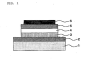
- Figure 1 shows a cross-sectional view of an example of the organic light-emitting device according to the present invention.
- An organic light-emitting device of the present invention contains at least one organic layer sandwiched between an anode and a cathode, wherein at least one layer of the organic layers contains a light-emitting layer.
- FIG. 1 One example of the configuration of the organic light-emitting device is illustrated in Figure 1 , though the configuration of the device is not restricted to it.
- Figure 1 between an anode (2) and a cathode (6) provided on a transparent substrate (1), a hole transport layer (3), a light-emitting layer (4), and an electron transport layer (5) are provided in this order.
- a hole transport layer/a light-emitting layer or 2) a light-emitting layer/an electron transport layer, or 3) only a light-emitting layer may be provided between the anode (2) and the cathode (6).
- a hole transport layer/a light-emitting layer or 2) a light-emitting layer/an electron transport layer, or 3) only a light-emitting layer may be provided between the anode (2) and the cathode (6).
- an anode buffer layer may be provided between the anode (2) and the hole transport layer (3)
- a hole blocking layer may be provided between the light-emitting layer (4) and the electron transport layer (5).
- a layer containing a compound having a hole transport property, a compound having a light emitting property, and a compound having an electron transport property 5) a layer containing a compound having a hole transport property and a compound having a light-emitting property, 6) a layer containing a compound having a light-emitting property and a compound having an electron transport property, or 7) a layer containing a compound having both a hole transport property and an electron transport property and a compound having a light-emitting property.
- Each of the layers may be formed by mixing polymer materials as binders.
- polymer materials include Poly(methylmethacrylate), polycarbonate, polyesters, polysulfones, and poly(phenylene oxide).
- At least one compound selected from the group consisting of a compound having an electron transport property, a compound having a hole transport property, and a compound having a light-emitting property may be also referred to as an organic electroluminescence compound (also organic EL compound in this specification), and a layer comprising the compound may be also referred to as an organic EL compound layer.
- a compound having a hole transport property, a compound having an electron transport property, and a compound having both a hole transport property and an electron transport property may be also referred to as a compound having carrier transport property.
- the light-emitting layer used in the present invention is a light-emitting layer containing a compound (a2) and a polymer compound (II), or a light-emitting layer that contains the compound (a2), the polymer compound (II) and the compound (d).
- the light-emitting layer [A] comprises the polymer compound (I) that contains a structural unit derived from the polymerizable compound (a1) and a structural unit derived from the polymerizable compound (b).
- the polymer compound (I) is obtained by copolymerizing the polymerizable compound (a1) and the polymerizable compound (b).
- the polymerizable compound (a1) has one carrier transport property either of a hole transport property or an electron transport property and a phosphorescent property, and is selected from the group consisting of the formulae (E1-1) to (E1-39). That is, the polymerizable compound (a1) is a hole transport or electron transport and phosphorescent compound.
- the polymerizable compound (a1) may be used solely or in a combination of two kinds or more if they have the same carrier transport property.
- At least one of the hydrogen atoms represents a substituent selected from the group consisting of a halogen atom, a cyano group, an alkyl group having 1 to 10 carbon atoms, an aryl group having 6 to 10 carbon atoms, an amino group optionally substituted with an alkyl group having 1 to 10 carbon atoms, an alkoxy group having 1-10 carbon atoms, and a silyl group.
- halogen atom examples include fluorine, chlorine, bromine, and iodine.
- alkyl group having 1 to 10 carbon atoms examples include methyl, ethyl, propyl, isopropyl, butyl, isobutyl, t-butyl, amyl, hexyl, octyl, and decyl.
- aryl group having 6 to 10 carbon atoms examples include phenyl, tolyl, xylyl, mesityl, and naphtyl.
- Examples of such amino group optionally substituted with an alkyl group having 1 to 10 carbon atoms include amino, dimethylamino, diethylamino, and dibutylamino.
- alkoxy group having 1 to 10 carbon atoms examples include methoxy, ethoxy, propoxy, isopropoxy, butoxy, isobutoxy, t-butoxy, hexyloxy, 2-ethylhexyloxy, and decyloxy.
- silyl group examples include trimethylsilyl, triethylsilyl, and t-butyldimethylsilyl.
- fluorine atom an alkyl group having 1 to 4 carbon atoms, phenyl group, tolyl group, dimethylamino group, and an alkoxy group having 1 to 4 carbon atoms are preferable, and fluorine atom, t-butyl group, dimethylamino group, and methoxy group are more preferable.
- one of the hydrogen atoms represents a polymerizable substituent represented by the formula (H1).
- R 25 represents a hydrogen atom or a linear alkyl group having 1 to 5 carbon atoms. Among them, methyl, ethyl, and propyl groups are preferable.
- the polymerizable substituent may be a substituent such as the one that is bonded to an iridium complex through an organic group composed of only hydrocarbons having 1 to 20 carbon atoms without containing heteroatoms.
- the substituents represented by the following general formulae (A1) to (A11) are preferably used.
- the polymerizable compound (b) has one carrier transport property either of a hole transport property or an electron transport property. That is, the polymerizable compound (b) is a hole transport or electron transport compound.
- the polymerizable compound (b) may not be restricted as long as it contains a polymerizable substituent, and a publicly known compound having the carrier transport property are used.
- the polymerizable compound (b) may be used solely or in a combination of two kinds or more if they have the same carrier transport property.
- the aforementioned polymerizable substituents have the same meanings as the polymerizable substituents in the polymerizable compound represented by the formula (E1-1), and so is the preferred range.
- a compound represented by the following formulae (F1) to (F9) is preferably used.
- polymerizable compound (b) having the electron transport property a compound represented by the following formulae (G1) to (G9) is preferably used.
- a polymerizable substituent is represented by the formula (A1) in the formulae (F1) to (F9) and (G1) to (G9), a polymerizable substituent represented by the aforementioned formula (H1) may be sufficient.
- the polymerizable compound (a1) is the hole transport or electron transport and phosphorescent compound, and the polymerizable compound (b) is capable of transporting the oppositely charged carrier.
- the polymerizable compound (a1) has the hole transport property as the carrier transport property as well as the phosphorescent property
- the polymerizable compound (b) has the electron transport property as the carrier transport property
- the polymerizable compound (b) has the hole transport property as the carrier transport property.
- a polymer compound having all functions of the phosphorescent property, the hole transport property, and the electron transport property can be obtained by merely copolymerizing the two kinds of compounds, respectively.
- a polymer compound having excellent durability can be obtained, since it suffices to use fewer kinds of compounds used as monomers. Also, adjustment of the energy levels is easier than the conventional ones, since it suffices to select only two kinds of compounds.
- the polymerizable compound (a1) has both functions of the carrier transport property and the phosphorescent property, a higher probability of generating excitons on the structural unit derived from the polymerizable compound (a1) and a higher luminous efficiency can be obtained.
- a combination of a polymerizable compound represented by the formula (E1-1), in particular by the following formula (E1-1-1) having the hole transport property and the phosphorescent property as the polymerizable compound (a1) and the polymerizable compound (b) having the electron transport property is the most preferable, since a device with excellent luminous efficiency and excellent durability can be obtained.
- R 1 1 to R 1 24 represents a substituent selected from the group consisting of a halogen atom, a cyano group, an alkyl group having 1 to 10 carbon atoms, an aryl group having 6 to 10 carbon atoms, an amino group optionally substituted with an alkyl group having 1 to 10 carbon atoms, an alkoxy group having 1 to 10 carbon atoms, and a silyl group.
- R 1 to R 1 24 represents a polymerizable substituent. Such polymerizable substituents have the same meanings as the aforementioned substituents, and so is the preferred range.
- a polymerizable compound having the carrier transport property in terms of both the hole transport property and the electron transport property that is, the polymerizable compound having the properties generally called "bipolar character" may be used.
- the polymerizable compound having the bipolar character is generally superior in either the hole transport property or the electron transport property, so that when this compound is used, the carrier balance is adjusted in accordance with the carrier transport property of the polymerizable compound (a1).
- Examples of such polymerizable compound having the bipolar character include 4,4'-N,N' -dicarbazolebiphenyl (CBP) .
- the polymer compound (I) contains preferably 3 to 60 wt%, more preferably 15 to 30 wt%, of the structural unit derived from the polymerizable compound (a1) with respect to the total structural units.
- the amount of the structural units is a value measured by the ICP elemental analysis and the 13 C-NMR measurement.
- a light-emitting layer with excellent film-formability and excellent durability can be obtained even though it contains larger amount of the structural units derived from the polymerizable compound (a1), since the polymerizable compound (a1) has the specific substituents as mentioned above. Also, the concentration quenching can be suppressed and higher luminous efficiency can be attained.
- the molecular weight of the polymer compound (I) is preferably 1,000 to 2,000,000, more preferably 20,000 to 100, 000 in terms of the weight-average molecular weight.
- the weight-average molecular weight is a value measured at 40°C by the gel-permeation chromatography method (GPC) using tetrahydrofuran as a solvent.
- the polymer compound (I) may be any of a random copolymer, a block copolymer, and an alternative copolymer.
- Polymerization methods to obtain the polymer compound (I) may be any of radical polymerization, cationic polymerization, anionic polymerization, and addition polymerization, though radical polymerization is preferable. These polymerization methods are disclosed more specifically, for example, in Japanese Patent Laid-Open Publication No. 2003-342325 , Japanese Patent Laid-Open Publication No. 2003-119179 , Japanese Patent Laid-Open Publication No. 2003-113246 , Japanese Patent Laid-Open Publication No. 2003-206320 , Japanese Patent Laid-Open Publication No. 2003-147021 , Japanese Patent Laid-Open Publication No. 2003-171391 , Japanese Patent Laid-Open Publication No. 2004-346312 , Japanese Patent Laid-Open Publication No. 2005-97589 .
- a solution dissolving the polymer compound (I) is prepared.
- the solvents for the preparation of the solution include, for example, chlorine-containing solvents such as chloroform, methylene chloride, and dichloroethane, ether solvents such as tetrahydrofuran, and anisole, aromatic hydrocarbon solvents such as toluene, and xylene, ketone solvents such as acetone, and methyl ethyl ketone, and ester solvents such as ethyl acetate, butyl acetate, and ethylcellosolve acetate.
- the prepared solution is coated on a substrate by wet-coating methods such as spin-coating, casting, microgravure coating, gravure coating, bar coating, roll coating, wire bar coating, dip coating, spray coating, screen printing, flexo printing, offset printing, and ink jet printing.
- wet-coating methods such as spin-coating, casting, microgravure coating, gravure coating, bar coating, roll coating, wire bar coating, dip coating, spray coating, screen printing, flexo printing, offset printing, and ink jet printing.
- the solution contains preferably the polymer compound (I) in an amount of 0.5 to 5 wt%.
- the light-emitting layer [B] contains the compound (a2) and the polymer compound (II) having a structural unit derived from the polymerizable compound (b).
- the polymer compound (II) is obtained by polymerizing the polymerizable compound (b).
- the compound (a2) used in the present invention has a hole transport property and a phosphorescent property, and is represented by the formula (E2-1-1). That is, the compound (a2) is a hole transport and phosphorescent compound.
- the compound (a2) may be used solely or in a combination of two kinds or more so long as they have the same kind of the carrier transport property.
- At least one of the hydrogen atoms is a substituent selected from the group consisting of a halogen atom, a cyano group, an alkyl group having 1 to 10 carbon atoms, an aryl group having 6 to 10 carbon atoms, an amino group optionally substituted with an alkyl group having 1 to 10 carbon atoms, an alkoxy group having 1 to 10 carbon atoms, and a silyl group.
- a substituent selected from the group consisting of a halogen atom, a cyano group, an alkyl group having 1 to 10 carbon atoms, an aryl group having 6 to 10 carbon atoms, an amino group optionally substituted with an alkyl group having 1 to 10 carbon atoms, an alkoxy group having 1 to 10 carbon atoms, and a silyl group.
- Preferable substituents are the same as those in the formula (E1-1).
- the polymerizable compound (b) used in the present invention has an electron transport property. That is, the polymerizable compound (b) is an electron transport compound.
- the polymerizable compound (b) is not particularly restricted except that it contains a polymerizable substituent, and a publicly known compound having the carrier transport property can be used.
- the polymerizable compound (b) may be used solely or in a combination of two kinds or more so long as they have the same kind of the carrier transport property.
- the aforementioned polymerizable substituents have the same meanings as the polymerizable substituents in the polymerizable compound represented by the formula (E1-1), and so is the preferred range.
- a compound represented by the formulae (F1) to (F9) is preferably used, and as the polymerizable compound (b) having the electron transport property, a compound represented by the formulae (G1) to (G9) is preferably used. While a polymerizable substituent is represented by the formula (A1) in the formulae (F1) to (F9) and (G1) to (G9), a polymerizable substituent represented by the formula (H1) may be sufficient.
- the molecular weight of the polymer compound (II) is preferably 1,000 to 2,000,000, more preferably 20,000 to 100, 000 in terms of the weight-average molecular weight.
- the weight-average molecular weight is a value measured at 40°C by the gel-permeation chromatography method (GPC) using tetrahydrofuran as a solvent.
- the polymerization methods to obtain the polymer compound (II) may be any of radical polymerization, cationic polymerization, anionic polymerization, and addition polymerization, though radical polymerization is preferable. These polymer compounds can be obtained by publicly known methods.
- the compound (a2) has the hole transport property as the carrier transport property as well as the phosphorescent property
- the polymerizable compound (b) has the electron transport property as the carrier transport property.
- a light-emitting layer having all functions of the phosphorescent property, the hole transport property, and the electron transport property can be obtained by using only two kinds of compounds, respectively. Because of this, it has excellent durability. When compared with the conventional methods, adjustment of the energy levels is easier, since it suffices to select only two kinds of compounds. Further, since the compound (a2) has both the carrier transport property and the phosphorescent property, a higher probability of generating excitons on the compound (a2) and a higher luminous efficiency can be obtained.
- the light-emitting layer used in the present invention a combination of a compound represented by the following formula (E2-1-1) having the hole transport property and the phosphorescent property as the compound (a2) and the polymer compound (II) containing a structural unit derived from the polymerizable compound (b) having the electron transport property is employed, since a device with excellent luminous efficiency and excellent durability can be obtained.
- a compound represented by the following formula (E2-1-1) having the hole transport property and the phosphorescent property as the compound (a2) and the polymer compound (II) containing a structural unit derived from the polymerizable compound (b) having the electron transport property is employed, since a device with excellent luminous efficiency and excellent durability can be obtained.
- At least one of R 2 1 to R 2 24 represents an alkyl group having 1 to 10 carbon atoms.
- a polymerizable compound having the carrier transport property in terms of both the hole transport property and the electron transport property that is, the polymerizable compound having the property generally called "bipolar character" may be used.
- the polymerizable compound having the bipolar character is generally superior in either the hole transport property or the electron transport property, so that when this compound is used, the carrier balance is adjusted in accordance with the carrier transport property of the compound (a2).
- Examples of such polymerizable compound having the bipolar character include 4,4'-N,N'-dicarbazolebiphenyl (CBP) .
- the light-emitting layer [B] contains 15 to 30 wt% of the compound (a2) with respect to the total amount of the compound (a2) and the polymer compound (II). Because the compound (a2) used in the present invention has the specific substituent as mentioned above, it has excellent film-formability and especially excellent dispersibility, thus it can be used in high concentration. Also, the compound (a2) has excellent dispersibility, so that a light-emitting layer with excellent durability can be obtained. Furthermore, it can suppress the concentration quenching and attain higher luminous efficiency.
- the methods to prepare the light-emitting layer [B] are not particularly restricted, and for example, it may be prepared by the following method. First, a solution dissolving the compound (a2) and the polymer compound (II) is prepared. The solvents used for the preparation of the solution are not particularly restricted, and the same solvents used in the case of the light-emitting layer [A] are used. Then, the prepared solution is coated on a substrate by the similar way as in the case of the light-emitting layer [A].
- the solution contains solid components in the concentration of 0.5 to 5 wt%, and the compound (a2) in an amount of 15 to 30 wt% and the polymer compound (II) in an amount of 85 to 70 wt% with respect to the total solid components.
- the light-emitting layer [C] preferably contains the compound (d) having the phosphorescent property that emits light at lower energy than the polymerizable compound (a1).
- the polymer compound (I) is used as a host. Because the polymer compound (I) is superior in durability and the carrier transport property, the energy transfer to the compound (d) takes place efficiently and the compound (d) emits light at high efficiency.
- any compound can be used without restriction so far as it emits light at lower energy than the polymerizable compound (a1).
- the compound (d) may be used solely or in a combination of two kinds or more.
- the energy at which a compound emits light refers to the excitation energy that is determined based on the absorption wavelength or emission wavelength measured by a spectrophotometer.
- the light-emitting layer [C] contains preferably 99.5 to 80 wt% of the polymer compound (I) and 0.5 to 20 wt% of the compound (d) with respect to the total amount of the polymer compound (I) and the compound (d).
- the methods to prepare the light-emitting layer [C] they are not particularly restricted, and for example, it may be prepared by the following method. First, a solution dissolving the polymer compound (I) and the compound (d) is prepared. The solvents used for the preparation of the solution are not particularly restricted, and the same solvents used in the case of the light-emitting layer [A] are used. Then, the prepared solution is coated on a substrate by the similar way as in the case of the light-emitting layer [A].
- the solution contains solid components in the concentration of 0.5 to 5 wt%, preferably the polymer compound (I) in an amount of 99.5 to 80 wt% and the compound (d) in an amount of 0.5 to 20 wt% with respect to the total solid components.
- the light-emitting layer [D] preferably contains the compound (d) having the phosphorescent property that emits light at a lower energy than the compound (a2).
- the compound (a2) and the polymer compound (II) are used as hosts. Because a light-emitting layer comprising the compound (a2) and the polymer compound (II) is superior in durability and the carrier transport property, the energy transfer to the compound (d) takes place efficiently and the compound (d) emits light at high efficiency.
- any compound that emits light at lower energy than the compound (a2) can be used without restriction.
- the compound (d) may be used solely or in a combination of two kinds or more.
- the light-emitting layer [D] contains preferably 15 to 30 wt% of the compound (a2), 70 to 85 wt% of the polymer compound (II), and 0.5 to 20 wt% of the compound (d) with respect to the total amount of the compound (a2), the polymer compound (II), and the compound (d).
- the methods to prepare the light-emitting layer [D] they are not particularly restricted, and for example, it may be prepared by the following method. First, a solution dissolving the compound (a2), the polymer compound (II), and the compound (d) is prepared. The solvents used for the preparation of the solution are not particularly restricted, and the same solvents used in the case of the light-emitting layer [A] are used. Then, the prepared solution is coated on a substrate by the similar way as in the case of the light-emitting layer [A].
- the solution contains solid components in the concentration of 0.5 to 5 wt%, preferably the compound (a2) in an amount of 15 to 30 wt%, the polymer compound (II) in an amount of 70 to 85 wt%, and the compound (d) in an amount of 0.5 to 20 wt% with respect to the total solid components.
- any compound used for the anode buffer layer any compound may be used without particular restriction so far as it has good adhesiveness to an anode surface and its overlying layers, and there may be mentioned, for example, publicly known conductive polymers, such as a mixture of poly(ethylenedioxythiophene) (PEDOT) andpoly(styrenesulfonic acid) (PSS) or a mixture (PANI) of polyaniline and poly(styrenesulfonate salts) Organic solvents such as toluene as isopropyl alcohol may be added to these conductive polymers. Also, conductive polymers may contain the third components such as surfactants.
- PEDOT poly(ethylenedioxythiophene)
- PSS poly(styrenesulfonic acid)
- PANI mixture
- Organic solvents such as toluene as isopropyl alcohol may be added to these conductive polymers.
- conductive polymers may contain the third components such as surfactants.
- surfactants there may be mentioned, for example, surfactants that contain alkyl groups, alkylaryl groups, fluoroalkyl groups, alkylsiloxane groups, sulfate salts, sulfonate salts, carboxylates, amides, betaine structure, or quaternary ammonium group, and fluoride-based nonionic surfactants may be also used.
- a hole block layer may be provided adjacent to the cathode side of the light-emitting layer.
- a compound with a lower Highest Occupied Molecular Orbital (HOMO) level than a light-emitting compound is used, and specifically, examples of such compounds include triazole derivatives, oxadiazole derivatives, phenanthroline derivatives or aluminum complexes .
- an exciton block layer may be provided adjacent to the cathode side of the light-emitting layer.
- a compound having an energy of the excited triplet state higher than that of the light-emitting compounds is used, and specifically, examples of such compounds include triazole derivatives, phenanthroline derivatives or aluminum complexes.
- the aforementioned layers may be formed by the dry-film forming methods, such as resistance heating vapor deposition, electron beam vapor deposition or sputtering, and also by the wet-film forming methods, such as spin-coating, casting, microgravure coating, gravure coating, bar coating, roll coating, wire bar coating, dip coating, spray coating, screen printing, flexo printing, offset printing, and ink jet printing.
- dry-film forming methods are preferably used, and in the case of high molecular weight compounds, wet-film forming methods are preferably used.
- anode materials relating to the organic light-emitting device of the present invention when observing the light emission through a substrate, for example, publicly known transparent conductive materials such as ITO (indium tin oxide), tin oxides, zinc oxides, and conductive polymers such as polythiophenes, polypyrroles or polyanilines are preferably used. Also, a thin metal film having a thickness of 1 to 3 nm may be provided on the ITO surface without impairing the optical transparency. Examples of such metals include gold, nickel, manganese, iridium, molybdenum, palladium, and platinum .
- anode materials for example, metals or metal compounds having the work function higher than 4.1 eV are preferably used, and metals similar to the aforementioned metals are specifically used. These metals may be used solely or in a combination of two kinds or more.
- the surface resistance of the anode is preferably 1 to 50 ⁇ / ⁇ (ohms/square), and the thickness of the anode is preferably 2 to 300 nm.
- the film-forming methods for the anode include, for example, vacuum vapor deposition, electron beam vapor deposition, sputtering, chemical reaction and coating methods .
- the properties of the anode buffer layer are improved by pre-treatment of the anode surface.
- pre-treatments include high-frequency plasma treatment, and such treatments as sputtering, corona treatment, UV ozone irradiation or oxygen plasma treatment .
- the cathode materials relating to the organic light-emitting device of the present invention materials are not specially restricted so long as they have low work function and are chemically stable.
- alkali metals such as Li, Na, K, and Cs
- alkaline earth metals such as Mg, Ca, and Ba, Al
- MgAg alloys alloys of Al and alkali metals such as AlLi and AlCa are preferably used.
- materials having the work function of 2.9 eV or lower are preferred.
- the thickness of the cathode is preferably 10 nm to 1 ⁇ m, and more preferably 50 to 500nm.
- the film-forming methods for the cathode materials for example, such methods as resistant heating vapor deposition, electron beam vapor deposition, sputtering or ion plating are used.
- a cathode buffer layer may be provided.
- this cathode buffer layer a layer of metals having lower work function than the cathode is used, and is inserted between the cathode and the organic layer adjacent to the cathode.
- the metals used for the cathode buffer layer there may be mentioned, for example, alkali metals (Na, K, Rb, Cs), alkaline earth metals (Sr, Ba, Ca, Mg), and rare earth metals (Pr, Sm, Eu, Yb).
- the thickness of the cathode buffer layer is preferably 0.05 to 50 nm, more preferably 0.1 to 20 nm, and most preferably 0.5 to 10 nm.
- the cathode buffer layer may be formed as a mixture between the metal having low work function and a compound having an electron transport property.
- the compound having the electron transport property the aforementioned compounds shown as examples are used.
- the thickness of such cathode buffer layer is preferably 0.1 to 100 nm, more preferably 0.5 to 50 nm, and most preferably 1 to 20 nm.
- a layer comprising a conductive polymer, a layer comprising a metal oxide, a metal fluoride, and an organic insulating material may be provided between the cathode and the organic layer.
- the film-forming methods of the cathode buffer layer such methods as vapor deposition, vapor co-deposition or sputtering are used. Also, depending on the materials used, such film-forming methods as spin coating, dip coating, ink jet coating, printing, spraying or dispenser are used.
- an insulating substrate that is transparent to the emission wavelength of the aforementioned light-emitting material is preferably used.
- transparent plastics as PET (polyethylene terephthalate) or polycarbonate are used.
- a protection layer and/or a protection cover may be provided. In this way, the durability of the organic light-emitting device is improved.
- a protection layer a layer comprising a polymer compound, a metal oxide, a metal fluoride or a metal borate is used.
- the protection cover such materials as a glass plate, a plastic plate whose surface is treated for low water-permeation or a metal are used, and methods for sealing by pasting said cover with the device substrate by using a thermosetting resin or a photo-setting resin are preferably employed.
- the device becomes resistant to chipping. If inert gases such as nitrogen or argon are filled in this space, oxidation of the cathode can be prevented. Further, if drying agents such as barium oxide and the like are provided in the space, the damage to the device due to moisture adsorbed during manufacturing processes can be suppressed. Among these measures, it is recommended to employ one measure or more.
- patterned emission by using the organic light-emitting device of the present invention such methods that provide a mask having a patterned window on the surface of the above planar light-emitting device, form the organic substance layer of the non-emitting part extremely thick to make substantially non-emitting, and form a patterned anode and/or a cathode are employed.
- a segment-type display device can be obtained. In this way, a display device that can display numbers, letters and simple symbols can be obtained.
- both anode and cathode are formed in stripes and arranged orthogonally to each other.
- use of a color filter or a fluorescence conversion filter, partial color display or multi-color display may become possible.
- the dot matrix device may be applied to a passive drive or an active drive in combination with TFT
- These display devices may be preferably used as the display devices in computers, televisions, mobile terminals, cell phones, car navigation systems, and view finders of video cameras .
- planar anode and a planar cathode are arranged in such a way to be overlaid.
- these planer light-emitting devices are of the self-emitting thin type, they are preferably used as a surface-emitting light source, a back light for the display devices such as liquid crystal display devices, planar illuminating devices, interiors, and exteriors.
- a flexible substrate it can be used as a light source or a display device with curved surfaces.
- ITO indium tin oxide (anode)
- an organic light-emitting device was prepared by using an ITO (indium tin oxide)-attached substrate (Nippo Electric Co., Ltd.) on which two lines of ITO electrodes each having a width of 4 mm were provided.
- ITO indium tin oxide
- poly(3,4-ethylenedioxythiophene)/poly(styrenesulfonic acid) (trade name "BAYTRON P", manufactured by Bayer AG) was applied on the ITO (anode) of the ITO-attached substrate by spin coating method at a rotation speed of 3500 rpm and a coating time of 40 seconds, followed by drying at 100°C for 2 hours under reduced pressure in a vacuum desiccator to form an anode buffer layer.
- the thickness of the obtained anode buffer layer was about 60 nm.
- a coating solution to form a layer that contains the phosphorescent compound was prepared. Namely, 11.5 mg of polydi[4-(3,5-dimethyl-p-terphenyl)]-2,6-dimethyl-4-styrylphenyl borane (abbreviated as poly-(vi2MB)), which is a polymer compound having the electron transport property, and 1.3 mg of tris(4-tert-butylphenylpyridine)iridium (III) (abbreviated as G3), which is a compound (a dye) having the hole transport property and the phosphorescent property were dissolved in 387.2 mg of toluene (guaranteed reagent, Wako Pure Chemical Industries, Ltd.), and then the obtained solution was filtered through a filter with 0.2 ⁇ m pour diameter to obtain the coating solution.
- poly-(vi2MB) polydi[4-(3,5-dimethyl-p-terphenyl)]-2,6-dimethyl-4-sty
- the dye concentration contained in the coating solution was 10% with respect to the solid components. Then, the prepared coating solution was applied on the anode buffer layer with spin coating method under the conditions of a rotation speed of 3000 rpm and a coating time of 30 seconds, followed by drying at 140°C for 30 minutes to obtain a light-emitting layer.
- the thickness of the obtained light-emitting layer was about 80 nm.
- the substrate on which the light-emitting layer was formed was mounted in a vapor deposition apparatus, vapor-deposited with barium at the vapor deposition speed of 0.01 nm/s up to 2 nm thickness, followed by vapor deposition with aluminum as the cathode at the vapor deposition speed of 1 nm/s up to 150 nm thickness to obtain device 1.
- the layers of barium and aluminum were formed in 2 lines each with 3 mm width arranged orthogonally with respect to the lengthwise direction of the anode to prepare 4 pieces of organic light-emitting devices with 4 mm long x 3 mm wide per one sheet of the glass substrate.
- devices 2 to 4 were prepared in the same way as device 1 except that the concentration of the dye (G3) in the solid components was varied to 20%, 30%, and 40%.
- the results of the measurements of EL light emitting properties of these devices performed in the same way as device 1 are also shown in Table 3.
- devices 5 to 8 were prepared in the same way as device 1 except that poly(N,N'-(3-methylphenyl)-N-phenyl-N'-(3-vinylphenyl)-1,1' -biphenyl-4,4'-diamine-Co-di[4-(3,5-dimethyl-p-terphenyl)]-2,6-dimethyl-4-styrylphenyl borane) (poly- (HMTPD) -poly- (vi2MB)) was used in the coating solution instead of the polymer compound having the electron transport property (poly-(vi2MB)) used for device 1.
- a coating solution was prepared in which another dye was further added to the coating solution used in Example 1 containing the compound having the electron transport property and the phosphorescent compound (dye). Namely, 70 mg of poly-(vi2MB), 19.2 mg of G3 dye, and 6.7 mg of [6-(4-vinylphenyl)-2,4-hexanedionato]bis[2-(2-pyridyl)benzo thienyl] iridium (III) (abbreviated as R3) were dissolved in 2. 9 g of toluene, and the obtained solution was filtered through a filter with the pore diameter of 0.2 ⁇ m to obtain the coating solution. The dye concentrations contained in the solution were 20% for G3 and 7% for R3 with respect to the solid components. All procedures other than those for preparing the composition of the coating solution were performed according to Example 1 to obtain device 9.
- Example 2 As illustrated in Table 5, it is evident that the light-emitting device (Example 2) prepared by adding further R3 dye having a lower emission energy than G3 dye to the system in which the phosphorescent compound (G3 dye) was added in high concentration to the polymer having the electron transport property, showed higher external quantum efficiency and better durability than the light-emitting device (Comparative Example 2) prepared by adding the phosphorescent compound (R3 dye) to the copolymer of the compound having the hole transport property and the compound having the electron transport property.
Landscapes
- Chemical & Material Sciences (AREA)
- Engineering & Computer Science (AREA)
- Materials Engineering (AREA)
- Organic Chemistry (AREA)
- Electroluminescent Light Sources (AREA)
- Addition Polymer Or Copolymer, Post-Treatments, Or Chemical Modifications (AREA)
Claims (4)
- Organisches Leuchtelement, enthaltend ein oder mehrere organische Schichten, die sich zwischen einer Anode und einer Kathode befinden, wobei zumindest eine Schicht der organischen Schichten eine Licht-emittierende Schicht ist, umfassend eine Verbindung (a2), welches eine Lochtransportund phosphoreszierende Verbindung ist, und eine Polymerverbindung (II), bestehend aus Struktureinheiten, die von einer polymerisierbaren Verbindung (b) abgeleitet sind, bei der es sich um eine Elektronen-transportierende Verbindung handelt, wobei die Verbindung (a2) durch folgende Formel (E2-1-1) dargestellt wird:

- Organisches Leuchtelement nach Anspruch 1, wobei die Licht-emittierende Schicht eine phosphoreszierende Verbindung (d) enthält, welche Licht bei einer niedrigeren Energie abgibt als die Verbindung (a2).
- Bildanzeigevorrichtung, bei der das organische Leuchtelement nach Anspruch 1 oder 2 verwendet wird.
- Oberflächen-emittierende Lichtquelle, bei der das organische Leuchtelement nach Anspruch 1 oder 2 verwendet wird.
Applications Claiming Priority (2)
| Application Number | Priority Date | Filing Date | Title |
|---|---|---|---|
| JP2006085639A JP4994688B2 (ja) | 2006-03-27 | 2006-03-27 | キャリア輸送性および燐光発光性を有する化合物を用いた有機発光素子 |
| PCT/JP2007/057330 WO2007119629A1 (en) | 2006-03-27 | 2007-03-26 | An organic light-emitting device using a compound having a carrier transport property and a phosphorescent property |
Publications (2)
| Publication Number | Publication Date |
|---|---|
| EP1999227A1 EP1999227A1 (de) | 2008-12-10 |
| EP1999227B1 true EP1999227B1 (de) | 2011-10-19 |
Family
ID=38236444
Family Applications (1)
| Application Number | Title | Priority Date | Filing Date |
|---|---|---|---|
| EP07740766A Active EP1999227B1 (de) | 2006-03-27 | 2007-03-26 | Organische leuchtdiode, die eine verbindung mit einer trägerstofftransporteigenschaft und einer phosphoreszenzeigenschaft einsetzt |
Country Status (8)
| Country | Link |
|---|---|
| US (1) | US8268456B2 (de) |
| EP (1) | EP1999227B1 (de) |
| JP (1) | JP4994688B2 (de) |
| KR (1) | KR101035453B1 (de) |
| CN (1) | CN101410477A (de) |
| AT (1) | ATE529493T1 (de) |
| TW (1) | TWI418074B (de) |
| WO (1) | WO2007119629A1 (de) |
Families Citing this family (13)
| Publication number | Priority date | Publication date | Assignee | Title |
|---|---|---|---|---|
| WO2009092671A2 (en) * | 2008-01-25 | 2009-07-30 | Basf Se | Organic light emitting systems |
| US8808878B2 (en) | 2008-11-28 | 2014-08-19 | Riken | Compound and use thereof |
| KR101219668B1 (ko) | 2010-05-14 | 2013-01-18 | 주식회사 씨유전자 | 청색 인광 이리듐 유기착화합물 및 이를 포함하는 유기전기발광소자 |
| CN102082232A (zh) * | 2010-09-16 | 2011-06-01 | 昆山维信诺显示技术有限公司 | 一种蓝光有机电致发光器件 |
| US9310050B2 (en) | 2010-09-28 | 2016-04-12 | Koninklijke Philips N.V. | Light-emitting arrangement with organic phosphor |
| CN102603802B (zh) * | 2011-12-22 | 2014-09-10 | 南京邮电大学 | 以噻吩基苯并噻唑衍生物为配体的磷光铱配合物及制备和应用 |
| CN103497219A (zh) * | 2013-10-12 | 2014-01-08 | 北京科技大学 | 一类红光铱配合物及其在有机电致白或红发光器件中应用 |
| CN103819511A (zh) * | 2014-02-28 | 2014-05-28 | 上海和辉光电有限公司 | 一种聚集诱导磷光发射铱配合物及其电致发光器件 |
| JP5880679B2 (ja) * | 2014-07-16 | 2016-03-09 | 住友化学株式会社 | 発光素子の製造方法 |
| KR102383852B1 (ko) * | 2014-10-08 | 2022-04-07 | 엘지디스플레이 주식회사 | 인광 화합물 및 이를 이용한 유기발광다이오드소자 |
| US10950803B2 (en) * | 2014-10-13 | 2021-03-16 | Universal Display Corporation | Compounds and uses in devices |
| CN107532013A (zh) | 2015-01-30 | 2018-01-02 | 默克专利有限公司 | 具有低粒子含量的制剂 |
| US11753425B2 (en) | 2018-07-11 | 2023-09-12 | Universal Display Corporation | Organic electroluminescent materials and devices |
Family Cites Families (25)
| Publication number | Priority date | Publication date | Assignee | Title |
|---|---|---|---|---|
| JPH07301714A (ja) * | 1994-05-09 | 1995-11-14 | Beam Soken:Kk | 面放光装置 |
| US8206838B2 (en) * | 2000-06-12 | 2012-06-26 | Sumitomo Chemical Co., Ltd. | Polymer matrix electroluminescent materials and devices |
| SG92833A1 (en) | 2001-03-27 | 2002-11-19 | Sumitomo Chemical Co | Polymeric light emitting substance and polymer light emitting device using the same |
| KR100376286B1 (ko) | 2001-03-29 | 2003-03-17 | 광주과학기술원 | 비닐-페닐 피리딘 단량체와 이를 이용하여 제조한 고분자 |
| ATE431970T1 (de) * | 2001-06-20 | 2009-06-15 | Showa Denko Kk | Licht emittierendes material und organische leuchtdiode |
| KR100937900B1 (ko) * | 2001-08-29 | 2010-01-21 | 유니버시티 오브 서던 캘리포니아 | 금속착물을 포함하는 캐리어수송층을 구비한 유기발광장치 |
| JP4574936B2 (ja) * | 2001-08-31 | 2010-11-04 | 日本放送協会 | 燐光発光性化合物及び燐光発光性組成物 |
| US7250226B2 (en) | 2001-08-31 | 2007-07-31 | Nippon Hoso Kyokai | Phosphorescent compound, a phosphorescent composition and an organic light-emitting device |
| CN100371370C (zh) * | 2001-09-04 | 2008-02-27 | 佳能株式会社 | 高分子化合物以及有机发光元件 |
| JP2003073479A (ja) | 2001-09-04 | 2003-03-12 | Canon Inc | 高分子化合物及び有機発光素子 |
| AU2003211786A1 (en) | 2002-03-08 | 2003-09-22 | Canon Kabushiki Kaisha | Organic light-emitting device |
| JP2005528759A (ja) * | 2002-05-31 | 2005-09-22 | コーニンクレッカ フィリップス エレクトロニクス エヌ ヴィ | 電界発光デバイス |
| JP2004018787A (ja) * | 2002-06-19 | 2004-01-22 | Fuji Photo Film Co Ltd | カルバゾール誘導体、並びにそのポリマー、及びそれを含有する発光素子 |
| JP4203732B2 (ja) * | 2003-06-12 | 2009-01-07 | ソニー株式会社 | 有機電界発光材料、有機電界発光素子および含複素環イリジウム錯体化合物 |
| TWI267545B (en) * | 2003-06-17 | 2006-12-01 | Univ Tsinghua | Electroluminescent conjugated polymers containing phosphorescent moieties and the application thereof in LED |
| JP4321808B2 (ja) * | 2003-11-11 | 2009-08-26 | 大日本印刷株式会社 | 有機エレクトロルミネッセンス素子および表示用パネル |
| JP5051565B2 (ja) * | 2003-12-10 | 2012-10-17 | 奇美電子股▲ふん▼有限公司 | 画像表示装置 |
| TW200528536A (en) * | 2003-12-19 | 2005-09-01 | Showa Denko Kk | Boron-containing polymer compound and organic light emitting device using the same |
| JP2005306998A (ja) * | 2004-04-21 | 2005-11-04 | Jsr Corp | 電荷輸送性重合体およびその製造方法、並びに有機エレクトロルミネッセンス素子用重合体組成物および有機エレクトロルミネッセンス素子 |
| US20050253510A1 (en) * | 2004-05-11 | 2005-11-17 | Shogo Nasu | Light-emitting device and display device |
| EP1753839B1 (de) * | 2004-05-21 | 2011-07-20 | Showa Denko K.K. | Polymeres lichtemittierendes material und organisches lichtemittierendes element |
| JP2006013222A (ja) * | 2004-06-28 | 2006-01-12 | Fuji Photo Film Co Ltd | 有機電界発光素子、およびその製造方法 |
| JP4544937B2 (ja) * | 2004-07-30 | 2010-09-15 | 大日本印刷株式会社 | 有機機能素子、有機el素子、有機半導体素子、有機tft素子およびそれらの製造方法 |
| JP5130606B2 (ja) * | 2005-02-25 | 2013-01-30 | コニカミノルタホールディングス株式会社 | 有機エレクトロルミネッセンス素子、その製造方法、表示装置及び照明装置 |
| US20080061686A1 (en) * | 2006-03-22 | 2008-03-13 | Jie Liu | Phosphorescent light-emitting materials and methods of preparing |
-
2006
- 2006-03-27 JP JP2006085639A patent/JP4994688B2/ja active Active
-
2007
- 2007-03-26 EP EP07740766A patent/EP1999227B1/de active Active
- 2007-03-26 AT AT07740766T patent/ATE529493T1/de not_active IP Right Cessation
- 2007-03-26 CN CNA2007800107365A patent/CN101410477A/zh active Pending
- 2007-03-26 WO PCT/JP2007/057330 patent/WO2007119629A1/en active Application Filing
- 2007-03-26 US US12/281,544 patent/US8268456B2/en active Active
- 2007-03-26 KR KR1020087026148A patent/KR101035453B1/ko active IP Right Grant
- 2007-03-27 TW TW096110632A patent/TWI418074B/zh active
Also Published As
| Publication number | Publication date |
|---|---|
| KR20090005064A (ko) | 2009-01-12 |
| KR101035453B1 (ko) | 2011-05-18 |
| JP2007266071A (ja) | 2007-10-11 |
| TWI418074B (zh) | 2013-12-01 |
| EP1999227A1 (de) | 2008-12-10 |
| TW200810172A (en) | 2008-02-16 |
| US8268456B2 (en) | 2012-09-18 |
| WO2007119629A1 (en) | 2007-10-25 |
| US20090058286A1 (en) | 2009-03-05 |
| JP4994688B2 (ja) | 2012-08-08 |
| ATE529493T1 (de) | 2011-11-15 |
| CN101410477A (zh) | 2009-04-15 |
Similar Documents
| Publication | Publication Date | Title |
|---|---|---|
| EP1999227B1 (de) | Organische leuchtdiode, die eine verbindung mit einer trägerstofftransporteigenschaft und einer phosphoreszenzeigenschaft einsetzt | |
| WO2009122876A1 (ja) | 有機エレクトロルミネッセンス素子およびその製造方法 | |
| JP5610382B2 (ja) | 発光素子 | |
| CN102106017A (zh) | 有机电致发光元件、有机电致发光显示装置以及有机电致发光光源 | |
| JP2007161860A (ja) | 高分子発光材料、有機エレクトロルミネッセンス素子および表示装置 | |
| EP1902076B1 (de) | Lichtemittierendes polymermaterial, organische elektrolumineszente vorrichtung und anzeigevorrichtung mit lichtemittierendem polymermaterial | |
| EP1969083B1 (de) | Organische lichtemittierende vorrichtung | |
| EP1915789B1 (de) | Organische elektrolumineszenzvorrichtung unter verwendung eines copolymers und einer phosphoreszierenden iridiumverbindung | |
| EP2075311B1 (de) | Organisches leuchtbauelement | |
| EP3262127B1 (de) | Phosphoreszierende tinte | |
| JP5031276B2 (ja) | 高分子発光材料、ならびに高分子発光材料を用いた有機エレクトロルミネッセンス素子および表示装置 | |
| TWI605071B (zh) | 有機發光裝置 | |
| JP4823601B2 (ja) | 高分子発光材料、有機エレクトロルミネッセンス素子、および表示装置 | |
| JP2007165606A (ja) | 有機発光素子 | |
| JP2007084612A (ja) | 高分子発光材料、有機エレクトロルミネッセンス素子および表示装置 | |
| EP2835839B1 (de) | Organisches elektrolumineszenzelement und verfahren zur herstellung davon | |
| JP5466747B2 (ja) | 高分子化合物 | |
| JP5759670B2 (ja) | 有機発光素子 | |
| JP2007220351A (ja) | 有機エレクトロルミネッセンス素子およびその用途 | |
| EP2835840B1 (de) | Organisches elektrolumineszentes element und verfahren zur herstellung davon |
Legal Events
| Date | Code | Title | Description |
|---|---|---|---|
| PUAI | Public reference made under article 153(3) epc to a published international application that has entered the european phase |
Free format text: ORIGINAL CODE: 0009012 |
|
| 17P | Request for examination filed |
Effective date: 20081013 |
|
| AK | Designated contracting states |
Kind code of ref document: A1 Designated state(s): AT BE BG CH CY CZ DE DK EE ES FI FR GB GR HU IE IS IT LI LT LU LV MC MT NL PL PT RO SE SI SK TR |
|
| 17Q | First examination report despatched |
Effective date: 20090324 |
|
| GRAP | Despatch of communication of intention to grant a patent |
Free format text: ORIGINAL CODE: EPIDOSNIGR1 |
|
| GRAS | Grant fee paid |
Free format text: ORIGINAL CODE: EPIDOSNIGR3 |
|
| RIN1 | Information on inventor provided before grant (corrected) |
Inventor name: IGARASHI, TAKESHI Inventor name: KOYAMA, TAMAMI |
|
| RAP1 | Party data changed (applicant data changed or rights of an application transferred) |
Owner name: SHOWA DENKO K.K. |
|
| GRAA | (expected) grant |
Free format text: ORIGINAL CODE: 0009210 |
|
| DAX | Request for extension of the european patent (deleted) | ||
| RAP1 | Party data changed (applicant data changed or rights of an application transferred) |
Owner name: SHOWA DENKO K.K. |
|
| AK | Designated contracting states |
Kind code of ref document: B1 Designated state(s): AT BE BG CH CY CZ DE DK EE ES FI FR GB GR HU IE IS IT LI LT LU LV MC MT NL PL PT RO SE SI SK TR |
|
| REG | Reference to a national code |
Ref country code: GB Ref legal event code: FG4D |
|
| REG | Reference to a national code |
Ref country code: CH Ref legal event code: EP |
|
| REG | Reference to a national code |
Ref country code: IE Ref legal event code: FG4D |
|
| REG | Reference to a national code |
Ref country code: DE Ref legal event code: R096 Ref document number: 602007018057 Country of ref document: DE Effective date: 20111215 |
|
| REG | Reference to a national code |
Ref country code: NL Ref legal event code: VDEP Effective date: 20111019 |
|
| LTIE | Lt: invalidation of european patent or patent extension |
Effective date: 20111019 |
|
| REG | Reference to a national code |
Ref country code: AT Ref legal event code: MK05 Ref document number: 529493 Country of ref document: AT Kind code of ref document: T Effective date: 20111019 |
|
| PG25 | Lapsed in a contracting state [announced via postgrant information from national office to epo] |
Ref country code: IS Free format text: LAPSE BECAUSE OF FAILURE TO SUBMIT A TRANSLATION OF THE DESCRIPTION OR TO PAY THE FEE WITHIN THE PRESCRIBED TIME-LIMIT Effective date: 20120219 Ref country code: BE Free format text: LAPSE BECAUSE OF FAILURE TO SUBMIT A TRANSLATION OF THE DESCRIPTION OR TO PAY THE FEE WITHIN THE PRESCRIBED TIME-LIMIT Effective date: 20111019 Ref country code: LT Free format text: LAPSE BECAUSE OF FAILURE TO SUBMIT A TRANSLATION OF THE DESCRIPTION OR TO PAY THE FEE WITHIN THE PRESCRIBED TIME-LIMIT Effective date: 20111019 |
|
| PG25 | Lapsed in a contracting state [announced via postgrant information from national office to epo] |
Ref country code: PT Free format text: LAPSE BECAUSE OF FAILURE TO SUBMIT A TRANSLATION OF THE DESCRIPTION OR TO PAY THE FEE WITHIN THE PRESCRIBED TIME-LIMIT Effective date: 20120220 Ref country code: SE Free format text: LAPSE BECAUSE OF FAILURE TO SUBMIT A TRANSLATION OF THE DESCRIPTION OR TO PAY THE FEE WITHIN THE PRESCRIBED TIME-LIMIT Effective date: 20111019 Ref country code: SI Free format text: LAPSE BECAUSE OF FAILURE TO SUBMIT A TRANSLATION OF THE DESCRIPTION OR TO PAY THE FEE WITHIN THE PRESCRIBED TIME-LIMIT Effective date: 20111019 Ref country code: LV Free format text: LAPSE BECAUSE OF FAILURE TO SUBMIT A TRANSLATION OF THE DESCRIPTION OR TO PAY THE FEE WITHIN THE PRESCRIBED TIME-LIMIT Effective date: 20111019 Ref country code: GR Free format text: LAPSE BECAUSE OF FAILURE TO SUBMIT A TRANSLATION OF THE DESCRIPTION OR TO PAY THE FEE WITHIN THE PRESCRIBED TIME-LIMIT Effective date: 20120120 Ref country code: NL Free format text: LAPSE BECAUSE OF FAILURE TO SUBMIT A TRANSLATION OF THE DESCRIPTION OR TO PAY THE FEE WITHIN THE PRESCRIBED TIME-LIMIT Effective date: 20111019 |
|
| PG25 | Lapsed in a contracting state [announced via postgrant information from national office to epo] |
Ref country code: CY Free format text: LAPSE BECAUSE OF FAILURE TO SUBMIT A TRANSLATION OF THE DESCRIPTION OR TO PAY THE FEE WITHIN THE PRESCRIBED TIME-LIMIT Effective date: 20111019 |
|
| PG25 | Lapsed in a contracting state [announced via postgrant information from national office to epo] |
Ref country code: DK Free format text: LAPSE BECAUSE OF FAILURE TO SUBMIT A TRANSLATION OF THE DESCRIPTION OR TO PAY THE FEE WITHIN THE PRESCRIBED TIME-LIMIT Effective date: 20111019 Ref country code: EE Free format text: LAPSE BECAUSE OF FAILURE TO SUBMIT A TRANSLATION OF THE DESCRIPTION OR TO PAY THE FEE WITHIN THE PRESCRIBED TIME-LIMIT Effective date: 20111019 Ref country code: BG Free format text: LAPSE BECAUSE OF FAILURE TO SUBMIT A TRANSLATION OF THE DESCRIPTION OR TO PAY THE FEE WITHIN THE PRESCRIBED TIME-LIMIT Effective date: 20120119 Ref country code: CZ Free format text: LAPSE BECAUSE OF FAILURE TO SUBMIT A TRANSLATION OF THE DESCRIPTION OR TO PAY THE FEE WITHIN THE PRESCRIBED TIME-LIMIT Effective date: 20111019 Ref country code: SK Free format text: LAPSE BECAUSE OF FAILURE TO SUBMIT A TRANSLATION OF THE DESCRIPTION OR TO PAY THE FEE WITHIN THE PRESCRIBED TIME-LIMIT Effective date: 20111019 |
|
| PLBE | No opposition filed within time limit |
Free format text: ORIGINAL CODE: 0009261 |
|
| STAA | Information on the status of an ep patent application or granted ep patent |
Free format text: STATUS: NO OPPOSITION FILED WITHIN TIME LIMIT |
|
| PG25 | Lapsed in a contracting state [announced via postgrant information from national office to epo] |
Ref country code: IT Free format text: LAPSE BECAUSE OF FAILURE TO SUBMIT A TRANSLATION OF THE DESCRIPTION OR TO PAY THE FEE WITHIN THE PRESCRIBED TIME-LIMIT Effective date: 20111019 Ref country code: RO Free format text: LAPSE BECAUSE OF FAILURE TO SUBMIT A TRANSLATION OF THE DESCRIPTION OR TO PAY THE FEE WITHIN THE PRESCRIBED TIME-LIMIT Effective date: 20111019 Ref country code: PL Free format text: LAPSE BECAUSE OF FAILURE TO SUBMIT A TRANSLATION OF THE DESCRIPTION OR TO PAY THE FEE WITHIN THE PRESCRIBED TIME-LIMIT Effective date: 20111019 |
|
| 26N | No opposition filed |
Effective date: 20120720 |
|
| PG25 | Lapsed in a contracting state [announced via postgrant information from national office to epo] |
Ref country code: MC Free format text: LAPSE BECAUSE OF NON-PAYMENT OF DUE FEES Effective date: 20120331 |
|
| REG | Reference to a national code |
Ref country code: CH Ref legal event code: PL |
|
| REG | Reference to a national code |
Ref country code: DE Ref legal event code: R097 Ref document number: 602007018057 Country of ref document: DE Effective date: 20120720 |
|
| REG | Reference to a national code |
Ref country code: IE Ref legal event code: MM4A |
|
| PG25 | Lapsed in a contracting state [announced via postgrant information from national office to epo] |
Ref country code: CH Free format text: LAPSE BECAUSE OF NON-PAYMENT OF DUE FEES Effective date: 20120331 Ref country code: IE Free format text: LAPSE BECAUSE OF NON-PAYMENT OF DUE FEES Effective date: 20120326 Ref country code: AT Free format text: LAPSE BECAUSE OF FAILURE TO SUBMIT A TRANSLATION OF THE DESCRIPTION OR TO PAY THE FEE WITHIN THE PRESCRIBED TIME-LIMIT Effective date: 20111019 Ref country code: LI Free format text: LAPSE BECAUSE OF NON-PAYMENT OF DUE FEES Effective date: 20120331 |
|
| PG25 | Lapsed in a contracting state [announced via postgrant information from national office to epo] |
Ref country code: ES Free format text: LAPSE BECAUSE OF FAILURE TO SUBMIT A TRANSLATION OF THE DESCRIPTION OR TO PAY THE FEE WITHIN THE PRESCRIBED TIME-LIMIT Effective date: 20120130 |
|
| PG25 | Lapsed in a contracting state [announced via postgrant information from national office to epo] |
Ref country code: FI Free format text: LAPSE BECAUSE OF FAILURE TO SUBMIT A TRANSLATION OF THE DESCRIPTION OR TO PAY THE FEE WITHIN THE PRESCRIBED TIME-LIMIT Effective date: 20111019 |
|
| PG25 | Lapsed in a contracting state [announced via postgrant information from national office to epo] |
Ref country code: MT Free format text: LAPSE BECAUSE OF FAILURE TO SUBMIT A TRANSLATION OF THE DESCRIPTION OR TO PAY THE FEE WITHIN THE PRESCRIBED TIME-LIMIT Effective date: 20111019 |
|
| PG25 | Lapsed in a contracting state [announced via postgrant information from national office to epo] |
Ref country code: TR Free format text: LAPSE BECAUSE OF FAILURE TO SUBMIT A TRANSLATION OF THE DESCRIPTION OR TO PAY THE FEE WITHIN THE PRESCRIBED TIME-LIMIT Effective date: 20111019 |
|
| PG25 | Lapsed in a contracting state [announced via postgrant information from national office to epo] |
Ref country code: LU Free format text: LAPSE BECAUSE OF NON-PAYMENT OF DUE FEES Effective date: 20120326 |
|
| PG25 | Lapsed in a contracting state [announced via postgrant information from national office to epo] |
Ref country code: HU Free format text: LAPSE BECAUSE OF FAILURE TO SUBMIT A TRANSLATION OF THE DESCRIPTION OR TO PAY THE FEE WITHIN THE PRESCRIBED TIME-LIMIT Effective date: 20070326 |
|
| REG | Reference to a national code |
Ref country code: DE Ref legal event code: R082 Ref document number: 602007018057 Country of ref document: DE Representative=s name: PATENTANWAELTE RUFF, WILHELM, BEIER, DAUSTER &, DE |
|
| REG | Reference to a national code |
Ref country code: GB Ref legal event code: 732E Free format text: REGISTERED BETWEEN 20140731 AND 20140806 |
|
| REG | Reference to a national code |
Ref country code: DE Ref legal event code: R081 Ref document number: 602007018057 Country of ref document: DE Owner name: SAMSUNG ELECTRONICS CO., LTD., SUWON-SI, KR Free format text: FORMER OWNER: SHOWA DENKO K.K., TOKIO/TOKYO, JP Effective date: 20140818 Ref country code: DE Ref legal event code: R082 Ref document number: 602007018057 Country of ref document: DE Representative=s name: PATENTANWAELTE RUFF, WILHELM, BEIER, DAUSTER &, DE Effective date: 20140818 |
|
| REG | Reference to a national code |
Ref country code: FR Ref legal event code: TP Owner name: SAMSUNG ELECTRONICS CO., LTD., KR Effective date: 20141024 |
|
| REG | Reference to a national code |
Ref country code: FR Ref legal event code: PLFP Year of fee payment: 10 |
|
| REG | Reference to a national code |
Ref country code: FR Ref legal event code: PLFP Year of fee payment: 11 |
|
| REG | Reference to a national code |
Ref country code: FR Ref legal event code: PLFP Year of fee payment: 12 |
|
| PGFP | Annual fee paid to national office [announced via postgrant information from national office to epo] |
Ref country code: DE Payment date: 20240220 Year of fee payment: 18 Ref country code: GB Payment date: 20240220 Year of fee payment: 18 |
|
| PGFP | Annual fee paid to national office [announced via postgrant information from national office to epo] |
Ref country code: FR Payment date: 20240226 Year of fee payment: 18 |