EP1995779A2 - Leistungshalbleitermodul - Google Patents
Leistungshalbleitermodul Download PDFInfo
- Publication number
- EP1995779A2 EP1995779A2 EP08008716A EP08008716A EP1995779A2 EP 1995779 A2 EP1995779 A2 EP 1995779A2 EP 08008716 A EP08008716 A EP 08008716A EP 08008716 A EP08008716 A EP 08008716A EP 1995779 A2 EP1995779 A2 EP 1995779A2
- Authority
- EP
- European Patent Office
- Prior art keywords
- cup
- edge
- semiconductor module
- power semiconductor
- housing
- Prior art date
- Legal status (The legal status is an assumption and is not a legal conclusion. Google has not performed a legal analysis and makes no representation as to the accuracy of the status listed.)
- Granted
Links
Images

Classifications
-
- H—ELECTRICITY
- H10—SEMICONDUCTOR DEVICES; ELECTRIC SOLID-STATE DEVICES NOT OTHERWISE PROVIDED FOR
- H10W—GENERIC PACKAGES, INTERCONNECTIONS, CONNECTORS OR OTHER CONSTRUCTIONAL DETAILS OF DEVICES COVERED BY CLASS H10
- H10W76/00—Containers; Fillings or auxiliary members therefor; Seals
- H10W76/10—Containers or parts thereof
- H10W76/12—Containers or parts thereof characterised by their shape
- H10W76/15—Containers comprising an insulating or insulated base
-
- H—ELECTRICITY
- H05—ELECTRIC TECHNIQUES NOT OTHERWISE PROVIDED FOR
- H05K—PRINTED CIRCUITS; CASINGS OR CONSTRUCTIONAL DETAILS OF ELECTRIC APPARATUS; MANUFACTURE OF ASSEMBLAGES OF ELECTRICAL COMPONENTS
- H05K7/00—Constructional details common to different types of electric apparatus
- H05K7/02—Arrangements of circuit components or wiring on supporting structure
- H05K7/10—Plug-in assemblages of components, e.g. IC sockets
- H05K7/1053—Plug-in assemblages of components, e.g. IC sockets having interior leads
-
- H—ELECTRICITY
- H10—SEMICONDUCTOR DEVICES; ELECTRIC SOLID-STATE DEVICES NOT OTHERWISE PROVIDED FOR
- H10W—GENERIC PACKAGES, INTERCONNECTIONS, CONNECTORS OR OTHER CONSTRUCTIONAL DETAILS OF DEVICES COVERED BY CLASS H10
- H10W76/00—Containers; Fillings or auxiliary members therefor; Seals
- H10W76/60—Seals
-
- H—ELECTRICITY
- H10—SEMICONDUCTOR DEVICES; ELECTRIC SOLID-STATE DEVICES NOT OTHERWISE PROVIDED FOR
- H10W—GENERIC PACKAGES, INTERCONNECTIONS, CONNECTORS OR OTHER CONSTRUCTIONAL DETAILS OF DEVICES COVERED BY CLASS H10
- H10W90/00—Package configurations
Definitions
- the invention relates to a power semiconductor module having a substrate and a cup-shaped housing, wherein the cup edge of the housing is stepped with a peripheral raised outer edge and a recessed against the outer edge of the inner edge, which are interconnected by a grading surface.
- the substrate is preferably a DCB substrate (direct copper bonding substrates).
- Such a power semiconductor module is in the earlier patent application 10 2006 052 607.4 the applicant described.
- a production scrap is minimized by unintentionally rotating the substrate relative to the cup-shaped housing.
- This unwanted possible contact of the substrate with one of its corners with the associated corner region of the cup rim of the housing is caused, for example, by the fact that the substrate has relatively large dimensional tolerances of its outer edge.
- These dimensional tolerances are, for example, due to the fact that the substrate is usually produced by laser scribing from a correspondingly large multiple substrate, wherein the multiple substrate is formed with corresponding predetermined breaking lines by the said laser scribing, along which the multiple substrate in a number of substrates apart is broken.
- the invention has for its object to provide a power semiconductor module of the type mentioned above, wherein a contact of corners of the substrate with the associated corner regions of the cup rim of the housing prevents structurally simple means and a resulting production committee is avoided.
- the substrate has a square or at least approximately square base surface and the cup rim of the housing has a corresponding base configuration, it is preferred if the respective angled extension has two equal extension legs in the corner region of the cup rim of the housing. If the substrate has a rectangular basic surface shape, then the two extension legs of the angled extension are preferably dimensioned adapted to the length-to-width ratio of the substrate.
- the inner edge of the cup-shaped housing is formed with elevations and the outer edge with anti-rotation knobs, and if the substrate rests against the elevations with its edge region adjoining on its outer edge on the inside.
- Such a design provides the advantage that unwanted twisting of the substrate relative to the housing, i. is limited to the cup rim of the same defined by the anti-rotation nubs in each case.
- each extension leg has a leg section parallel to the associated grading surface and a conical section adjoining it.
- the two leg sections are preferably connected to one another by a radius section.
- the power semiconductor module according to the invention has the advantage that it is achieved in a structurally simple design in a simple manner that the substrate with the corners of its outer edge even with a utilization of the maximum allowable dimensional tolerances not scraping on the cup edge of the housing.
- Another advantage is that the inventive construction, for example, according to the DE 10 2004 021 927 A1 formed coating process of the substrate positively influenced because the applied to the substrate coating material in the corner area can not create the housing.
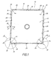
- FIG. 1 shows in a view from below an embodiment of the power semiconductor module 10 with a substrate 12 and a cup-shaped housing 14.
- the cup-shaped housing 14 has a peripheral cup edge 16 which is stepped with a peripheral raised outer edge 18 and a recessed against this inner edge 20 is formed.
- the raised outer edge 18 and the recessed inner edge 20 are connected together by a grading surface 22.
- the recessed inner edge 20 is formed with spaced elevations 24 and the raised outer edge 18 is formed with spaced anti-rotation nubs 26.
- the substrate 12 rests against the elevations 24 of the housing 14 with its edge region 30 of its upper side adjoining its outer edge 28.
- the grading surface 22 between the raised outer edge 18 and the recessed inner edge 20 of the cup-shaped housing 14 is in the corner regions 32 of the peripheral cup rim 16 of the cup-shaped Housing 14 each formed with a corner-shaped angled extension 34.
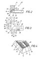
- the respective angled extension 34 has two mutually perpendicular extension legs 36, which in FIG. 3 are illustrated by the double arrows 36.
- the respective extension leg 36 has a leg section parallel to the associated step surface 22, which in FIG FIG. 3 is illustrated by the double arrows 38, and an adjoining cone section, which in FIG. 3 indicated by the double arrows 40.
- the two mutually perpendicular leg sections 38 are connected to each other by a radius section 42.
- the respective cone section 40 adjoins an associated anti-rotation knob 26.
- FIG. 1 a power semiconductor module 10 is shown, in which the substrate 12 with respect to the cup-shaped housing 14 and to its circumferential cup rim 16 due to the dimensional tolerances of the outer edge 28 of the substrate 12 and the peripheral cup edge 16 and thus the material from the elevated outer edge 18 centrein Serialig weg choir anti-rotation nubs 26th is slightly rotated in a clockwise direction, so that the outer edge 28 of the substrate 12 is applied only to a Verwarschommesnoppe 26, which is prevented by the formation of the stepped surface 22 in the corner regions 32 of the cup rim 16 each with an angularly angled extension 34, that the substrate 12th with its corners 44 comes into contact with the corner regions 34 of the peripheral cup edge 16 of the housing 14 and a resulting damage and thus a product failure is avoided.
Landscapes
- Engineering & Computer Science (AREA)
- Microelectronics & Electronic Packaging (AREA)
- Container, Conveyance, Adherence, Positioning, Of Wafer (AREA)
- Semiconductor Lasers (AREA)
- Rotary Pumps (AREA)
- Electroplating Methods And Accessories (AREA)
- Led Device Packages (AREA)
- Structures Or Materials For Encapsulating Or Coating Semiconductor Devices Or Solid State Devices (AREA)
Abstract
Description
- Die Erfindung betrifft ein Leistungshalbleitermodul mit einem Substrat und einem becherförmigen Gehäuse, wobei der Becherrand des Gehäuses abgestuft mit einem umlaufenden erhöhten Außenrand und einem gegen den Außenrand vertieften Innenrand ausgebildet ist, die durch eine Abstufungsfläche miteinander verbunden sind.
- Bei dem Substrat handelt es sich vorzugsweise um ein DCB-Substrat (Direct Copper Bonding-Substrate).
- Ein derartiges Leistungshalbleitermodul ist in der älteren Patentanmeldung
10 2006 052 607.4 - In Kenntnis dieser Gegebenheiten liegt der Erfindung die Aufgabe zugrunde, ein Leistungshalbleitermodul der eingangs genannten Art zu schaffen, wobei ein Kontakt von Ecken des Substrates mit den zugehörigen Eckenbereichen des Becherrandes des Gehäuses mit konstruktiv einfachen Mitteln verhindert und ein daraus resultierender Produktionsausschuss vermieden wird.
- Diese Aufgabe wird erfindungsgemäß durch die Merkmale des Anspruches 1, d.h. dadurch gelöst, dass die den erhöhten Außenrand mit dem vertieften Innenrand verbindende Abstufungsfläche des Becherrandes des Gehäuses in den Eckenbereichen des Becherrandes des Gehäuses jeweils mit einer eckkonform abgewinkelten Erweiterung ausgebildet ist.
- Durch die Ausbildung der Eckenbereiche des Becherrandes des Gehäuses mit den abgewinkelten Erweiterungen ergibt sich der Vorteil, dass die Ecken des Substrates jederzeit, d.h. auch dann von den Eckenbereichen des Becherrandes des Gehäuses beabstandet sind, wenn das Substrat gegen das Gehäuse, d.h. gegen den Becherrand des Gehäuses unbeabsichtigt verdreht ist.
- Weist das Substrat eine quadratische oder mindestens annähernd quadratische Grundfläche und der Becherrand des Gehäuses eine entsprechende Grundflächengestalt auf, so ist es bevorzugt, wenn die jeweilige abgewinkelte Erweiterung im Eckenbereich des Becherrandes des Gehäuses zwei gleich lange Erweiterungsschenkel aufweist. Besitzt das Substrat eine rechteckige Grundflächengestalt, so sind die beiden Erweiterungsschenkel der abgewinkelten Erweiterung vorzugsweise an das Längen-zu-Breiten-Verhältnis des Substrates angepasst dimensioniert.
- Bevorzugt ist es bei dem erfindungsgemäßen Leistungshalbleitermodul, wenn der Innenrand des becherförmigen Gehäuses mit Erhebungen und der Außenrand mit Verdrehsicherungsnoppen ausgebildet ist, und wenn das Substrat mit seinem an seinen Außenrand innenseitig angrenzenden Randbereich an den Erhebungen anliegt. Durch eine derartige Ausbildung ergibt sich der Vorteil, dass ein ungewollte Verdrehung des Substrates relativ zum Gehäuse, d.h. zum Becherrand desselben durch die Verdrehsicherungsnoppen in jedem Fall definiert begrenzt wird.
- Zweckmäßig kann es sein, wenn jeder Erweiterungsschenkel einen zur zugehörigen Abstufungsfläche parallelen Schenkelabschnitt und einen sich daran anschließenden Konusabschnitt aufweist. Die beiden Schenkelabschnitte sind vorzugsweise durch einen Radiusabschnitt miteinander verbunden.
- Als vorteilhaft hat es sich erwiesen, wenn der jeweilige Konusabschnitt an eine zugehörige Verdrehsicherungsnoppe angrenzt.
- Das erfindungsgemäße Leistungshalbleitermodul weist den Vorteil auf, dass bei einer konstruktiv einfachen Ausbildung auf einfache Weise erreicht wird, dass das Substrat mit den Ecken seines Außenrandes auch bei einer Ausnutzung der maximalen erlaubten Abmessungstoleranzen nicht am Becherrand des Gehäuses schabt. Ein weiterer Vorteil besteht darin, dass die erfindungsgemäße Ausbildung den beispielsweise gemäß der
DE 10 2004 021 927 A1 ausgebildeten Beschichtungsprozess des Substrates positiv beeinflusst, weil sich das auf das Substrat aufgebrachte Beschichtungsmaterial im Eckenbereich nicht am Gehäuse anlegen kann. - Weitere Einzelheiten, Merkmale und Vorteile ergeben sich aus der nachfolgenden Beschreibung eines in der Zeichnung dargestellten Ausführungsbeispieles eines erfindungsgemäßen Leistungshalbleitermoduls bzw. wesentlicher Einzelheiten desselben.
- Es zeigen:
- Figur 1
- eine Ansicht des Halbleitermoduls in Blickrichtung von unten,
- Figur 2
- schematisch abschnittweise stark vergrößert und nicht maßstabgetreu einen Schnitt entlang der Schnittlinie II-II in
Figur 1 , - Figur 3
- einen Abschnitt einer Ansicht des Becherrandes des Gehäuses in einem vergrößerten Maßstab und nicht maßstabgetreut in Blickrichtung von unten,
- Figur 4
- abschnittweise perspektivisch eine Ausbildung des becherförmigen Gehäuses,
- Figur 5
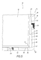
- in einem größeren Maßstab das Detail V in
Figur 1 , und - Figur 6
- in einem der
Figur 5 entsprechenden Maßstab das Detail VI inFigur 1 . -
Figur 1 zeigt in einer Ansicht von unten eine Ausbildung des Leistungshalbleitermoduls 10 mit einem Substrat 12 und einem becherförmigen Gehäuse 14. Wie auch aus denFiguren 2 bis 6 ersichtlich ist, weist das becherförmige Gehäuse 14 einen umlaufenden Becherrand 16 auf, der abgestuft mit einem umlaufenden erhöhten Außenrand 18 und einem gegen diesen vertieften Innenrand 20 ausgebildet ist. Der erhöhte Außenrand 18 und der vertiefte Innenrand 20 sind miteinander durch eine Abstufungsfläche 22 verbunden. - Der vertiefte Innenrand 20 ist mit voneinander beabstandeten Erhebungen 24 und der erhöhte Außenrand 18 ist mit voneinander beabstandeten Verdrehsicherungsnoppen 26 ausgebildet. Das Substrat 12 liegt mit seinem an seinen Außenrand 28 angrenzenden Randbereich 30 seiner Oberseite an den Erhebungen 24 des Gehäuses 14 an. Bei dem Substrat 12 handelt es sich vorzugsweise um ein DCB-Substrat (= Direct Copper Bonding-Substrate).
- Die Abstufungsfläche 22 zwischen dem erhöhten Außenrand 18 und dem vertieften Innenrand 20 des becherförmigen Gehäuses 14 ist in den Eckenbereichen 32 des umlaufenden Becherrandes 16 des becherförmigen Gehäuses 14 jeweils mit einer eckkonform abgewinkelten Erweiterung 34 ausgebildet. Die jeweilige abgewinkelte Erweiterung 34 weist zwei zueinander senkrecht orientierte Erweiterungsschenkel 36 auf, die in
Figur 3 durch die Doppelpfeile 36 verdeutlicht sind. Der jeweilige Erweiterungsschenkel 36 weist einen zur zugehörigen Abstufungsfläche 22 parallelen Schenkelabschnitt, der inFigur 3 durch die Doppelpfeile 38 verdeutlich ist, und einen sich daran anschließenden Konusabschnitt auf, der inFigur 3 durch die Doppelpfeile 40 angedeutet ist. Die beiden zueinander senkrecht orientierten Schenkelabschnitte 38 sind miteinander durch einen Radiusabschnitt 42 verbunden. Der jeweilige Konusabschnitt 40 grenzt an eine zugehörige Verdrehsicherungsnoppe 26 an. - In
Figur 1 ist ein Leistungshalbleitermodul 10 dargestellt, bei welchem das Substrat 12 in Bezug zum becherförmigen Gehäuse 14 bzw. zu dessen umlaufendem Becherrand 16 infolge der Abmessungstoleranzen des Außenrandes 28 des Substrats 12 und des umlaufenden Becherrandes 16 und somit den von dessen erhöhtem Außenrand 18 materialeinstückig wegstehenden Verdrehsicherungsnoppen 26 im Uhrzeigersinn geringfügig verdreht ist, so dass der Außenrand 28 des Substrats 12 nur jeweils an einer Verdrehsicherungsnoppe 26 anliegt, wobei durch die Ausbildung der Abstufungsfläche 22 in den Eckenbereichen 32 des Becherrandes 16 jeweils mit einer eckkonform abgewinkelten Erweiterung 34 verhindert wird, dass das Substrat 12 mit seinen Ecken 44 mit den Eckenbereichen 34 des umlaufenden Becherrandes 16 des Gehäuses 14 in Kontakt kommt und eine daraus resultierende Beschädigung und somit ein Produktsausfall vermieden wird. - Gleiche Einzelheiten sind in den
Figuren 1 bis 6 jeweils mit denselben Bezugsziffern bezeichnet, so dass es sich erübrigt, in Verbindung mit den Zeichnungsfiguren alle Einzelheiten jeweils detailliert zu beschreiben. -
- 10
- Leistungshalbleitermodul
- 12
- Substrat (von 10)
- 14
- becherförmiges Gehäuses (von 10)
- 16
- umlaufender Becherrand (von 14)
- 18
- erhöhter Außenrand (von 16)
- 20
- vertiefter Innenrand (von 16)
- 22
- Abstufungsfläche (zwischen 18 und 20)
- 24
- Erhebungen (an 20 für 12)
- 26
- Verdrehsicherungsnoppen (an 18 für 28)
- 38
- Außenrand (von 12)
- 30
- Randbereich (von 12)
- 32
- Eckenbereiche (von 16)
- 34
- abgewinkelte Erweiterung (von 22 bei 32)
- 36
- Erweiterungsschenkel (von 34)
- 38
- paralleler Schenkelabschnitt (von 36)
- 40
- Konusabschnitt (von 36)
- 42
- Radiusabschnitt (zwischen 38 und 38)
- 44
- Ecken (von 12)
Claims (6)
- Leistungshalbleitermodul (10) mit einem Substrat (12) und einem becherförmigen Gehäuse (14), wobei der Becherrand (16) des Gehäuses (14) abgestuft mit einem umlaufenden erhöhten Außenrand (18) und einem gegen den Außenrand (18) vertieften Innenrand (20) ausgebildet ist, die durch eine Abstufungsfläche (22) miteinander verbunden sind,
dadurch gekennzeichnet,
dass die Abstufungsfläche (22) in den Eckenbereichen (32) des Becherrandes (16) des Gehäuses (14) jeweils mit einer eckkonform abgewinkelten Erweiterung (34) ausgebildet ist. - Leistungshalbleitermodul (10) nach Anspruch 1,
dadurch gekennzeichnet,
dass der Innenrand (20) des becherförmigen Gehäuses (14) mit Erhebungen (24) und der Außenrand (18) mit Verdrehsicherungsnoppen. (26) ausgebildet ist, und dass das Substrat (12) mit seinem an seinen Außenrand (28) innenseitig angrenzenden Randbereichen (30) an den Erhebungen (24) anliegt. - Leistungshalbleitermodul (10) nach Anspruch 1,
dadurch gekennzeichnet,
dass die jeweilige abgewinkelte Erweiterung (34) zwei zueinander senkrecht orientierte Erweiterungsschenkel (36) aufweist. - Leistungshalbleitermodul (10) nach Anspruch 3,
dadurch gekennzeichnet,
dass jeder Erweiterungsschenkel (36) einen zur zugehörigen Abstufungsfläche (22) parallelen Schenkelabschnitt (38) und einen sich daran anschließenden Konusabschnitt (40) aufweist. - Leistungshalbleitermodul (10) nach Anspruch 4,
dadurch gekennzeichnet,
dass die beiden Schenkelabschnitte (38) durch einen Radiusabschnitt (42) miteinander verbunden sind. - Leistungshalbleitermodul (10) nach Anspruch 4,
dadurch gekennzeichnet,
dass der jeweilige Konusabschnitt (40) an eine zugehörige Verdrehsicherungsnoppe (26) angrenzt.
Applications Claiming Priority (1)
| Application Number | Priority Date | Filing Date | Title |
|---|---|---|---|
| DE102007024159A DE102007024159B3 (de) | 2007-05-24 | 2007-05-24 | Leistungshalbleitermodul |
Publications (3)
| Publication Number | Publication Date |
|---|---|
| EP1995779A2 true EP1995779A2 (de) | 2008-11-26 |
| EP1995779A3 EP1995779A3 (de) | 2011-01-05 |
| EP1995779B1 EP1995779B1 (de) | 2011-12-14 |
Family
ID=39711122
Family Applications (1)
| Application Number | Title | Priority Date | Filing Date |
|---|---|---|---|
| EP08008716A Active EP1995779B1 (de) | 2007-05-24 | 2008-05-09 | Leistungshalbleitermodul |
Country Status (5)
| Country | Link |
|---|---|
| EP (1) | EP1995779B1 (de) |
| CN (1) | CN101312166B (de) |
| AT (1) | ATE537559T1 (de) |
| DE (1) | DE102007024159B3 (de) |
| ES (1) | ES2379022T3 (de) |
Citations (1)
| Publication number | Priority date | Publication date | Assignee | Title |
|---|---|---|---|---|
| DE102004021927A1 (de) | 2004-05-04 | 2005-12-01 | Semikron Elektronik Gmbh & Co. Kg | Verfahren zur inneren elektrischen Isolation eines Substrats für ein Leistungshalbleitermodul |
Family Cites Families (8)
| Publication number | Priority date | Publication date | Assignee | Title |
|---|---|---|---|---|
| DE3604882A1 (de) * | 1986-02-15 | 1987-08-20 | Bbc Brown Boveri & Cie | Leistungshalbleitermodul und verfahren zur herstellung des moduls |
| KR940007004B1 (ko) * | 1988-05-06 | 1994-08-03 | 엠프 인코퍼레이티드 | 칩 캐리어 소켓의 개량된 보유수단 |
| JP3316714B2 (ja) * | 1994-05-31 | 2002-08-19 | 三菱電機株式会社 | 半導体装置 |
| DE19630173C2 (de) * | 1996-07-26 | 2001-02-08 | Semikron Elektronik Gmbh | Leistungsmodul mit Halbleiterbauelementen |
| EP0884781A3 (de) * | 1997-06-12 | 1999-06-30 | Hitachi, Ltd. | Leistungshalbleitermodul |
| JP3838571B2 (ja) * | 2003-08-14 | 2006-10-25 | 松下電器産業株式会社 | 固体撮像装置の製造方法 |
| DE102004018475A1 (de) * | 2004-04-16 | 2005-11-10 | eupec Europäische Gesellschaft für Leistungshalbleiter mbH | Leistungshalbleiteranordnung |
| DE102006052607A1 (de) * | 2006-11-08 | 2008-05-15 | Semikron Elektronik Gmbh & Co. Kg | Leistungsmodul |
-
2007
- 2007-05-24 DE DE102007024159A patent/DE102007024159B3/de active Active
-
2008
- 2008-05-09 AT AT08008716T patent/ATE537559T1/de active
- 2008-05-09 EP EP08008716A patent/EP1995779B1/de active Active
- 2008-05-09 ES ES08008716T patent/ES2379022T3/es active Active
- 2008-05-23 CN CN200810109175.0A patent/CN101312166B/zh active Active
Patent Citations (1)
| Publication number | Priority date | Publication date | Assignee | Title |
|---|---|---|---|---|
| DE102004021927A1 (de) | 2004-05-04 | 2005-12-01 | Semikron Elektronik Gmbh & Co. Kg | Verfahren zur inneren elektrischen Isolation eines Substrats für ein Leistungshalbleitermodul |
Also Published As
| Publication number | Publication date |
|---|---|
| CN101312166A (zh) | 2008-11-26 |
| EP1995779A3 (de) | 2011-01-05 |
| DE102007024159B3 (de) | 2008-11-06 |
| EP1995779B1 (de) | 2011-12-14 |
| ES2379022T3 (es) | 2012-04-20 |
| CN101312166B (zh) | 2012-02-29 |
| ATE537559T1 (de) | 2011-12-15 |
Similar Documents
| Publication | Publication Date | Title |
|---|---|---|
| DE69417988T2 (de) | Leiterplattenrandverbinder mit Kontakten von verminderten Teilung | |
| DE19829467A1 (de) | Kontaktträger insbesondere für einen dünnen Smart Card Connector | |
| DE2053568A1 (de) | Anschlußbuchsen fur integrierte Schaltungen und Verfahren zur gleich zeitigen Montage mehrerer Buchsen | |
| DE102009001698A1 (de) | Verbindermodul für Anwendungen mit höherer Belastung | |
| DE102010026027A1 (de) | Federkontakt | |
| DE3520519A1 (de) | Elektrischer stecker und verfahren zu seiner herstellung | |
| DE2138919A1 (de) | Kontaktmatte | |
| DE102019112523A1 (de) | Filterplatte für kunststoffverarbeitungsgeräte | |
| EP0351531A2 (de) | Elektronische Baueinheit | |
| EP1995779B1 (de) | Leistungshalbleitermodul | |
| DE10061533A1 (de) | Selbsttragende Kontaktfeder, insbesondere für einen Smartcard-Connector | |
| DE3933765C2 (de) | Dichtungselement und Verfahren zur Herstellung | |
| DE102006008444B4 (de) | Lochblech für Bauteile und Anlagen zur Bearbeitung von schüttfähigen Teilen | |
| EP0952765B1 (de) | Kontaktstreifen zum elektrischen Kontaktieren und/oder zur Erzielung einer gegen hochfrequente elektromagnetische Wellen dichten Verbindung sowie zugehörige Abschirmanordnung | |
| DE102005023031B4 (de) | Abschirmgehäuse | |
| DE102006005275B4 (de) | Kontaktiereinrichtung für eine Smartcard | |
| EP0593846A2 (de) | Abgedichtetes Gehäuse | |
| EP1917623B1 (de) | Kontaktträger für einen smart card connector | |
| WO2001013694A1 (de) | Abschirmung zum verhindern des durchtritts elektromagnetischer strahlung | |
| EP0663174B1 (de) | Küchengerät zum Schneiden von Obst, Gemüse oder dergleichen | |
| EP1811822B1 (de) | Lötbauteilanordnung | |
| WO2022243298A1 (de) | Optoelektronische baugruppe und verfahren zur herstellung | |
| DE2756501C2 (de) | Kontaktboden für Stoff- und Wärmetauscher | |
| DE20107140U1 (de) | Leiterplattenbaugruppe | |
| EP4161214A1 (de) | Heizeinrichtung und verfahren zur herstellung einer heizeinrichtung |
Legal Events
| Date | Code | Title | Description |
|---|---|---|---|
| PUAI | Public reference made under article 153(3) epc to a published international application that has entered the european phase |
Free format text: ORIGINAL CODE: 0009012 |
|
| AK | Designated contracting states |
Kind code of ref document: A2 Designated state(s): AT BE BG CH CY CZ DE DK EE ES FI FR GB GR HR HU IE IS IT LI LT LU LV MC MT NL NO PL PT RO SE SI SK TR |
|
| AX | Request for extension of the european patent |
Extension state: AL BA MK RS |
|
| PUAL | Search report despatched |
Free format text: ORIGINAL CODE: 0009013 |
|
| AK | Designated contracting states |
Kind code of ref document: A3 Designated state(s): AT BE BG CH CY CZ DE DK EE ES FI FR GB GR HR HU IE IS IT LI LT LU LV MC MT NL NO PL PT RO SE SI SK TR |
|
| AX | Request for extension of the european patent |
Extension state: AL BA MK RS |
|
| RIC1 | Information provided on ipc code assigned before grant |
Ipc: H01L 25/07 20060101ALN20101130BHEP Ipc: H01L 23/053 20060101AFI20101130BHEP |
|
| 17P | Request for examination filed |
Effective date: 20101217 |
|
| REG | Reference to a national code |
Ref country code: DE Ref legal event code: R079 Ref document number: 502008005817 Country of ref document: DE Free format text: PREVIOUS MAIN CLASS: H01L0025070000 Ipc: H01L0023053000 |
|
| RIC1 | Information provided on ipc code assigned before grant |
Ipc: H05K 7/10 20060101ALI20110721BHEP Ipc: H01L 23/053 20060101AFI20110721BHEP Ipc: H01L 23/10 20060101ALI20110721BHEP Ipc: H01L 25/07 20060101ALN20110721BHEP |
|
| GRAP | Despatch of communication of intention to grant a patent |
Free format text: ORIGINAL CODE: EPIDOSNIGR1 |
|
| AKX | Designation fees paid |
Designated state(s): AT BE BG CH CY CZ DE DK EE ES FI FR GB GR HR HU IE IS IT LI LT LU LV MC MT NL NO PL PT RO SE SI SK TR |
|
| GRAS | Grant fee paid |
Free format text: ORIGINAL CODE: EPIDOSNIGR3 |
|
| GRAA | (expected) grant |
Free format text: ORIGINAL CODE: 0009210 |
|
| AK | Designated contracting states |
Kind code of ref document: B1 Designated state(s): AT BE BG CH CY CZ DE DK EE ES FI FR GB GR HR HU IE IS IT LI LT LU LV MC MT NL NO PL PT RO SE SI SK TR |
|
| REG | Reference to a national code |
Ref country code: GB Ref legal event code: FG4D Free format text: NOT ENGLISH |
|
| REG | Reference to a national code |
Ref country code: CH Ref legal event code: EP |
|
| REG | Reference to a national code |
Ref country code: IE Ref legal event code: FG4D |
|
| REG | Reference to a national code |
Ref country code: CH Ref legal event code: NV Representative=s name: BRAUNPAT BRAUN EDER AG |
|
| REG | Reference to a national code |
Ref country code: DE Ref legal event code: R096 Ref document number: 502008005817 Country of ref document: DE Effective date: 20120308 |
|
| REG | Reference to a national code |
Ref country code: NL Ref legal event code: T3 |
|
| REG | Reference to a national code |
Ref country code: SK Ref legal event code: T3 Ref document number: E 11023 Country of ref document: SK Ref country code: SE Ref legal event code: TRGR |
|
| REG | Reference to a national code |
Ref country code: ES Ref legal event code: FG2A Ref document number: 2379022 Country of ref document: ES Kind code of ref document: T3 Effective date: 20120420 |
|
| PG25 | Lapsed in a contracting state [announced via postgrant information from national office to epo] |
Ref country code: LT Free format text: LAPSE BECAUSE OF FAILURE TO SUBMIT A TRANSLATION OF THE DESCRIPTION OR TO PAY THE FEE WITHIN THE PRESCRIBED TIME-LIMIT Effective date: 20111214 Ref country code: NO Free format text: LAPSE BECAUSE OF FAILURE TO SUBMIT A TRANSLATION OF THE DESCRIPTION OR TO PAY THE FEE WITHIN THE PRESCRIBED TIME-LIMIT Effective date: 20120314 |
|
| LTIE | Lt: invalidation of european patent or patent extension |
Effective date: 20111214 |
|
| PG25 | Lapsed in a contracting state [announced via postgrant information from national office to epo] |
Ref country code: SI Free format text: LAPSE BECAUSE OF FAILURE TO SUBMIT A TRANSLATION OF THE DESCRIPTION OR TO PAY THE FEE WITHIN THE PRESCRIBED TIME-LIMIT Effective date: 20111214 Ref country code: LV Free format text: LAPSE BECAUSE OF FAILURE TO SUBMIT A TRANSLATION OF THE DESCRIPTION OR TO PAY THE FEE WITHIN THE PRESCRIBED TIME-LIMIT Effective date: 20111214 Ref country code: GR Free format text: LAPSE BECAUSE OF FAILURE TO SUBMIT A TRANSLATION OF THE DESCRIPTION OR TO PAY THE FEE WITHIN THE PRESCRIBED TIME-LIMIT Effective date: 20120315 Ref country code: HR Free format text: LAPSE BECAUSE OF FAILURE TO SUBMIT A TRANSLATION OF THE DESCRIPTION OR TO PAY THE FEE WITHIN THE PRESCRIBED TIME-LIMIT Effective date: 20111214 |
|
| PG25 | Lapsed in a contracting state [announced via postgrant information from national office to epo] |
Ref country code: CY Free format text: LAPSE BECAUSE OF FAILURE TO SUBMIT A TRANSLATION OF THE DESCRIPTION OR TO PAY THE FEE WITHIN THE PRESCRIBED TIME-LIMIT Effective date: 20111214 |
|
| REG | Reference to a national code |
Ref country code: IE Ref legal event code: FD4D |
|
| PG25 | Lapsed in a contracting state [announced via postgrant information from national office to epo] |
Ref country code: BG Free format text: LAPSE BECAUSE OF FAILURE TO SUBMIT A TRANSLATION OF THE DESCRIPTION OR TO PAY THE FEE WITHIN THE PRESCRIBED TIME-LIMIT Effective date: 20120314 Ref country code: IS Free format text: LAPSE BECAUSE OF FAILURE TO SUBMIT A TRANSLATION OF THE DESCRIPTION OR TO PAY THE FEE WITHIN THE PRESCRIBED TIME-LIMIT Effective date: 20120414 Ref country code: IE Free format text: LAPSE BECAUSE OF FAILURE TO SUBMIT A TRANSLATION OF THE DESCRIPTION OR TO PAY THE FEE WITHIN THE PRESCRIBED TIME-LIMIT Effective date: 20111214 Ref country code: CZ Free format text: LAPSE BECAUSE OF FAILURE TO SUBMIT A TRANSLATION OF THE DESCRIPTION OR TO PAY THE FEE WITHIN THE PRESCRIBED TIME-LIMIT Effective date: 20111214 Ref country code: EE Free format text: LAPSE BECAUSE OF FAILURE TO SUBMIT A TRANSLATION OF THE DESCRIPTION OR TO PAY THE FEE WITHIN THE PRESCRIBED TIME-LIMIT Effective date: 20111214 |
|
| PG25 | Lapsed in a contracting state [announced via postgrant information from national office to epo] |
Ref country code: PT Free format text: LAPSE BECAUSE OF FAILURE TO SUBMIT A TRANSLATION OF THE DESCRIPTION OR TO PAY THE FEE WITHIN THE PRESCRIBED TIME-LIMIT Effective date: 20120416 Ref country code: RO Free format text: LAPSE BECAUSE OF FAILURE TO SUBMIT A TRANSLATION OF THE DESCRIPTION OR TO PAY THE FEE WITHIN THE PRESCRIBED TIME-LIMIT Effective date: 20111214 Ref country code: PL Free format text: LAPSE BECAUSE OF FAILURE TO SUBMIT A TRANSLATION OF THE DESCRIPTION OR TO PAY THE FEE WITHIN THE PRESCRIBED TIME-LIMIT Effective date: 20111214 |
|
| PLBE | No opposition filed within time limit |
Free format text: ORIGINAL CODE: 0009261 |
|
| STAA | Information on the status of an ep patent application or granted ep patent |
Free format text: STATUS: NO OPPOSITION FILED WITHIN TIME LIMIT |
|
| PG25 | Lapsed in a contracting state [announced via postgrant information from national office to epo] |
Ref country code: DK Free format text: LAPSE BECAUSE OF FAILURE TO SUBMIT A TRANSLATION OF THE DESCRIPTION OR TO PAY THE FEE WITHIN THE PRESCRIBED TIME-LIMIT Effective date: 20111214 |
|
| 26N | No opposition filed |
Effective date: 20120917 |
|
| BERE | Be: lapsed |
Owner name: SEMIKRON ELEKTRONIK G.M.B.H. & CO. KG Effective date: 20120531 |
|
| PG25 | Lapsed in a contracting state [announced via postgrant information from national office to epo] |
Ref country code: MC Free format text: LAPSE BECAUSE OF NON-PAYMENT OF DUE FEES Effective date: 20120531 |
|
| REG | Reference to a national code |
Ref country code: DE Ref legal event code: R097 Ref document number: 502008005817 Country of ref document: DE Effective date: 20120917 |
|
| PG25 | Lapsed in a contracting state [announced via postgrant information from national office to epo] |
Ref country code: BE Free format text: LAPSE BECAUSE OF NON-PAYMENT OF DUE FEES Effective date: 20120531 |
|
| PG25 | Lapsed in a contracting state [announced via postgrant information from national office to epo] |
Ref country code: FI Free format text: LAPSE BECAUSE OF FAILURE TO SUBMIT A TRANSLATION OF THE DESCRIPTION OR TO PAY THE FEE WITHIN THE PRESCRIBED TIME-LIMIT Effective date: 20111214 |
|
| PG25 | Lapsed in a contracting state [announced via postgrant information from national office to epo] |
Ref country code: MT Free format text: LAPSE BECAUSE OF FAILURE TO SUBMIT A TRANSLATION OF THE DESCRIPTION OR TO PAY THE FEE WITHIN THE PRESCRIBED TIME-LIMIT Effective date: 20111214 |
|
| PG25 | Lapsed in a contracting state [announced via postgrant information from national office to epo] |
Ref country code: TR Free format text: LAPSE BECAUSE OF FAILURE TO SUBMIT A TRANSLATION OF THE DESCRIPTION OR TO PAY THE FEE WITHIN THE PRESCRIBED TIME-LIMIT Effective date: 20111214 |
|
| PG25 | Lapsed in a contracting state [announced via postgrant information from national office to epo] |
Ref country code: LU Free format text: LAPSE BECAUSE OF NON-PAYMENT OF DUE FEES Effective date: 20120509 |
|
| REG | Reference to a national code |
Ref country code: AT Ref legal event code: MM01 Ref document number: 537559 Country of ref document: AT Kind code of ref document: T Effective date: 20130509 |
|
| PG25 | Lapsed in a contracting state [announced via postgrant information from national office to epo] |
Ref country code: HU Free format text: LAPSE BECAUSE OF FAILURE TO SUBMIT A TRANSLATION OF THE DESCRIPTION OR TO PAY THE FEE WITHIN THE PRESCRIBED TIME-LIMIT Effective date: 20080509 |
|
| PG25 | Lapsed in a contracting state [announced via postgrant information from national office to epo] |
Ref country code: AT Free format text: LAPSE BECAUSE OF NON-PAYMENT OF DUE FEES Effective date: 20130509 |
|
| REG | Reference to a national code |
Ref country code: FR Ref legal event code: PLFP Year of fee payment: 9 |
|
| REG | Reference to a national code |
Ref country code: FR Ref legal event code: PLFP Year of fee payment: 10 |
|
| PGFP | Annual fee paid to national office [announced via postgrant information from national office to epo] |
Ref country code: NL Payment date: 20170522 Year of fee payment: 10 |
|
| PGFP | Annual fee paid to national office [announced via postgrant information from national office to epo] |
Ref country code: SE Payment date: 20170523 Year of fee payment: 10 |
|
| REG | Reference to a national code |
Ref country code: CH Ref legal event code: PCAR Free format text: NEW ADDRESS: HOLEESTRASSE 87, 4054 BASEL (CH) |
|
| REG | Reference to a national code |
Ref country code: FR Ref legal event code: PLFP Year of fee payment: 11 |
|
| REG | Reference to a national code |
Ref country code: SE Ref legal event code: EUG Ref country code: NL Ref legal event code: MM Effective date: 20180601 |
|
| PG25 | Lapsed in a contracting state [announced via postgrant information from national office to epo] |
Ref country code: SE Free format text: LAPSE BECAUSE OF NON-PAYMENT OF DUE FEES Effective date: 20180510 Ref country code: SK Free format text: LAPSE BECAUSE OF NON-PAYMENT OF DUE FEES Effective date: 20180509 |
|
| REG | Reference to a national code |
Ref country code: SK Ref legal event code: MM4A Ref document number: E 11023 Country of ref document: SK Effective date: 20180509 |
|
| PG25 | Lapsed in a contracting state [announced via postgrant information from national office to epo] |
Ref country code: NL Free format text: LAPSE BECAUSE OF NON-PAYMENT OF DUE FEES Effective date: 20180601 |
|
| PGFP | Annual fee paid to national office [announced via postgrant information from national office to epo] |
Ref country code: DE Payment date: 20250402 Year of fee payment: 18 |
|
| PGFP | Annual fee paid to national office [announced via postgrant information from national office to epo] |
Ref country code: ES Payment date: 20250603 Year of fee payment: 18 |
|
| PGFP | Annual fee paid to national office [announced via postgrant information from national office to epo] |
Ref country code: IT Payment date: 20250422 Year of fee payment: 18 |
|
| PGFP | Annual fee paid to national office [announced via postgrant information from national office to epo] |
Ref country code: FR Payment date: 20250401 Year of fee payment: 18 |
|
| PGFP | Annual fee paid to national office [announced via postgrant information from national office to epo] |
Ref country code: CH Payment date: 20250601 Year of fee payment: 18 |
|
| REG | Reference to a national code |
Ref country code: DE Ref legal event code: R081 Ref document number: 502008005817 Country of ref document: DE Owner name: SEMIKRON DANFOSS ELEKTRONIK GMBH & CO. KG, DE Free format text: FORMER OWNER: SEMIKRON ELEKTRONIK GMBH & CO. KG, 90431 NUERNBERG, DE |
|
| REG | Reference to a national code |
Ref country code: DE Ref legal event code: R079 Ref document number: 502008005817 Country of ref document: DE Free format text: PREVIOUS MAIN CLASS: H01L0023053000 Ipc: H10W0076150000 |
|
| PGFP | Annual fee paid to national office [announced via postgrant information from national office to epo] |
Ref country code: GB Payment date: 20260324 Year of fee payment: 19 |