EP1981127B1 - Steckverbinder, insbesondere für Leiterplatten - Google Patents
Steckverbinder, insbesondere für Leiterplatten Download PDFInfo
- Publication number
- EP1981127B1 EP1981127B1 EP08102529.8A EP08102529A EP1981127B1 EP 1981127 B1 EP1981127 B1 EP 1981127B1 EP 08102529 A EP08102529 A EP 08102529A EP 1981127 B1 EP1981127 B1 EP 1981127B1
- Authority
- EP
- European Patent Office
- Prior art keywords
- plug connector
- locking device
- functional elements
- contacts
- locking
- Prior art date
- Legal status (The legal status is an assumption and is not a legal conclusion. Google has not performed a legal analysis and makes no representation as to the accuracy of the status listed.)
- Active
Links
Images


Classifications
-
- H—ELECTRICITY
- H01—ELECTRIC ELEMENTS
- H01R—ELECTRICALLY-CONDUCTIVE CONNECTIONS; STRUCTURAL ASSOCIATIONS OF A PLURALITY OF MUTUALLY-INSULATED ELECTRICAL CONNECTING ELEMENTS; COUPLING DEVICES; CURRENT COLLECTORS
- H01R13/00—Details of coupling devices of the kinds covered by groups H01R12/70 or H01R24/00 - H01R33/00
- H01R13/62—Means for facilitating engagement or disengagement of coupling parts or for holding them in engagement
- H01R13/639—Additional means for holding or locking coupling parts together, after engagement, e.g. separate keylock, retainer strap
-
- H—ELECTRICITY
- H01—ELECTRIC ELEMENTS
- H01R—ELECTRICALLY-CONDUCTIVE CONNECTIONS; STRUCTURAL ASSOCIATIONS OF A PLURALITY OF MUTUALLY-INSULATED ELECTRICAL CONNECTING ELEMENTS; COUPLING DEVICES; CURRENT COLLECTORS
- H01R13/00—Details of coupling devices of the kinds covered by groups H01R12/70 or H01R24/00 - H01R33/00
- H01R13/62—Means for facilitating engagement or disengagement of coupling parts or for holding them in engagement
- H01R13/627—Snap or like fastening
- H01R13/6275—Latching arms not integral with the housing
-
- H—ELECTRICITY
- H01—ELECTRIC ELEMENTS
- H01R—ELECTRICALLY-CONDUCTIVE CONNECTIONS; STRUCTURAL ASSOCIATIONS OF A PLURALITY OF MUTUALLY-INSULATED ELECTRICAL CONNECTING ELEMENTS; COUPLING DEVICES; CURRENT COLLECTORS
- H01R13/00—Details of coupling devices of the kinds covered by groups H01R12/70 or H01R24/00 - H01R33/00
- H01R13/64—Means for preventing incorrect coupling
- H01R13/641—Means for preventing incorrect coupling by indicating incorrect coupling; by indicating correct or full engagement
-
- H—ELECTRICITY
- H01—ELECTRIC ELEMENTS
- H01R—ELECTRICALLY-CONDUCTIVE CONNECTIONS; STRUCTURAL ASSOCIATIONS OF A PLURALITY OF MUTUALLY-INSULATED ELECTRICAL CONNECTING ELEMENTS; COUPLING DEVICES; CURRENT COLLECTORS
- H01R12/00—Structural associations of a plurality of mutually-insulated electrical connecting elements, specially adapted for printed circuits, e.g. printed circuit boards [PCB], flat or ribbon cables, or like generally planar structures, e.g. terminal strips, terminal blocks; Coupling devices specially adapted for printed circuits, flat or ribbon cables, or like generally planar structures; Terminals specially adapted for contact with, or insertion into, printed circuits, flat or ribbon cables, or like generally planar structures
- H01R12/70—Coupling devices
- H01R12/71—Coupling devices for rigid printing circuits or like structures
- H01R12/712—Coupling devices for rigid printing circuits or like structures co-operating with the surface of the printed circuit or with a coupling device exclusively provided on the surface of the printed circuit
- H01R12/716—Coupling device provided on the PCB
-
- H—ELECTRICITY
- H01—ELECTRIC ELEMENTS
- H01R—ELECTRICALLY-CONDUCTIVE CONNECTIONS; STRUCTURAL ASSOCIATIONS OF A PLURALITY OF MUTUALLY-INSULATED ELECTRICAL CONNECTING ELEMENTS; COUPLING DEVICES; CURRENT COLLECTORS
- H01R12/00—Structural associations of a plurality of mutually-insulated electrical connecting elements, specially adapted for printed circuits, e.g. printed circuit boards [PCB], flat or ribbon cables, or like generally planar structures, e.g. terminal strips, terminal blocks; Coupling devices specially adapted for printed circuits, flat or ribbon cables, or like generally planar structures; Terminals specially adapted for contact with, or insertion into, printed circuits, flat or ribbon cables, or like generally planar structures
- H01R12/70—Coupling devices
- H01R12/71—Coupling devices for rigid printing circuits or like structures
- H01R12/72—Coupling devices for rigid printing circuits or like structures coupling with the edge of the rigid printed circuits or like structures
- H01R12/722—Coupling devices for rigid printing circuits or like structures coupling with the edge of the rigid printed circuits or like structures coupling devices mounted on the edge of the printed circuits
- H01R12/724—Coupling devices for rigid printing circuits or like structures coupling with the edge of the rigid printed circuits or like structures coupling devices mounted on the edge of the printed circuits containing contact members forming a right angle
-
- H—ELECTRICITY
- H01—ELECTRIC ELEMENTS
- H01R—ELECTRICALLY-CONDUCTIVE CONNECTIONS; STRUCTURAL ASSOCIATIONS OF A PLURALITY OF MUTUALLY-INSULATED ELECTRICAL CONNECTING ELEMENTS; COUPLING DEVICES; CURRENT COLLECTORS
- H01R13/00—Details of coupling devices of the kinds covered by groups H01R12/70 or H01R24/00 - H01R33/00
- H01R13/66—Structural association with built-in electrical component
- H01R13/70—Structural association with built-in electrical component with built-in switch
- H01R13/703—Structural association with built-in electrical component with built-in switch operated by engagement or disengagement of coupling parts, e.g. dual-continuity coupling part
-
- H—ELECTRICITY
- H01—ELECTRIC ELEMENTS
- H01R—ELECTRICALLY-CONDUCTIVE CONNECTIONS; STRUCTURAL ASSOCIATIONS OF A PLURALITY OF MUTUALLY-INSULATED ELECTRICAL CONNECTING ELEMENTS; COUPLING DEVICES; CURRENT COLLECTORS
- H01R13/00—Details of coupling devices of the kinds covered by groups H01R12/70 or H01R24/00 - H01R33/00
- H01R13/66—Structural association with built-in electrical component
- H01R13/717—Structural association with built-in electrical component with built-in light source
Definitions
- the present invention relates to a connector according to the preamble of claim 1.
- Connectors of the aforementioned type are known from DE 202 01 609 U1 known.
- the state of the art is further on the DE 195 35 836 A1 as well as on the DE 93 11 457.5 directed.
- To call are also the DE 295 13 997 U1 and the DE 34 40 043 ,
- a plug connector is provided in which further, mutually corresponding functional elements are arranged in the region of the at least one locking device and / or the holding device (in particular in these devices).
- the further, mutually corresponding functional elements are arranged.
- electrically conductive contacts are closed and separated from each other.
- the light-conducting elements are interconnected and separated from each other.
- non-contacting elements acting by means of magnetic, capacitive or inductive fields such as reed contacts or the like, are activated or deactivated.
- electromagnetic or electromechanical elements serving as the functional elements are e.g. closed and separated.
- printed circuit board connector describes the generic name of the invention, which but an application in other applications should not be excluded, such as wall bushing in a device or a conductor-conductor connection, which is mounted for example on a mounting rail.
- the invention and its subclaims include, in addition to the combination of a component for the connection of conductors and a counterpart for the printed circuit board connection described by way of example also these and other application variants. This includes, for example, those not described here Combinations of two components with conductor connection for a so-called flying connection or coupling or the combination of two components with PCB connection for the connection of two printed circuit boards. All components in the plug-in area can also be implemented in inverted (socket strip for solder connection or pin strip for conductor connection) or hermaphroditic design.
- electromechanical (magnetic / inductive or thermoelectric) movable elements are actuated such that a release of the lock during this period of operation is not possible or effectively prevented.
- a total of a connector which is not part of the invention is referred to, which consists of a first connector part 2 and a second connector part 3, wherein the two connector parts 2 and 3 can be secured by locking slide 4 in the coupled state against unintentional release.
- the first connector part 2 is at the first connector part 2 to a so-called socket and the second connector part 3 to a so-called plug or pin part, in which case the first connector part 2, ie the socket part, a guide housing 5 with a guide channel 5a Recording and sliding guide of only one locking slide 4 are formed.
- the connector is designed as a printed circuit board connector for contacting a printed circuit board 25.
- a connector part 3 is arranged on the printed circuit board 25. It has four arranged in a row pin contacts 26 which are designed to be angled with one of its ends soldered to the circuit board 25, where they contact tracks, and with its other end a part of the mating contacts of the mating face of the second connector part 3 Form coupling with the mating face of the other connector part 2.
- socket contacts (not visible here) are arranged, which contact the contacts 26 of the second connector part 3 in the assembled state and which are provided with terminals 27, here by way of example screw, for connecting outgoing conductor (not shown here). Also, the terminals 27 are arranged in a row.
- the connector parts each have a housing 28, 29, wherein the only one (shown and preferred) or the two or more (not shown) locks - especially the locking slide 4 and the corresponding guide channel 5 - not laterally outside next to the row of the coupling contacts is / are arranged but in the row between each two of the contacts to be coupled together of the two connector parts 26 and 27th
- the number of locks or the locking slide 4 and guide channels 5a, 10 can be reduced to only a single one of these elements, since the lock is arranged optimized so that it optimally absorbs forces that can act on the connector ,
- a locking of the two connector parts 2 and 3 relative to each other may optionally be performed with two or more locking slides 4.
- only one or more or all or all locking slides can be assigned to these further functional elements, in particular contacts.
- this further embodiment can also be applied if two locking slides are arranged laterally next to the row of contacts to be connected to the connector parts.
- the guide channels 5a and 10 run perpendicular to the said coupling plane 6, so that correspondingly the locking slide or slides 4 are displaceable perpendicular to the coupling plane 6.
- Each locking slide 4 is provided at its end facing the second connector part 3 with a provided with a locking cam 7, resilient tongue 8.
- the locking projection 7 is seen to the free end face of the tongue 8 with an obliquely sloping inlet bevel 9.
- the resilient tongue 8 with the locking cam 7 is the insertion channel 10 of the second connector part 3 opposite, through which the locking cam 7 and a part of the resilient tongue 8 for the purpose of locking the two connector parts 2 and 3 in the second connector part 3 can be inserted until the Latching cams 7, the guide channel 5 end surrounding the end face 11 engages behind.
- This position is clear Figure 1d ,
- the resilient tongue 8 is formed on an actuating bracket 12 of the locking slide 4, wherein the actuating bracket 12 is outside the respective guide channel 5 of the first connector part 2 and is provided for ease of operation on its side facing away from the guide channel 5 top, for example, with ribs 13.
- ribs 13 As an alternative to these ribs, other means for improving the operation may also be provided here, for example molded knobs or the like.
- the displacement of the locking slide 4 is determined by the length of the boundary wall 16, abut the alternately the bracket portion 12a and the stop cam 17.
- the locking slide 4 may expediently be provided in the region opposite the boundary wall 16 with a stop cam 17, which then abuts in the locked state on one of the boundary wall 16 opposite side wall 18 of the guide housing 5.
- the locking slide 4 In the locked state, the locking slide 4 preferably ends flush with the end faces of the guide housing 5.
- This through-hole 20 can be used for an optional locking screw or alternatively here for another electrical functional element such as a contact 21, which contacts another functional element such as a mating contact 22 on the other connector part when pushing together or plugging the two connector parts.
- another electrical functional element such as a contact 21, which contacts another functional element such as a mating contact 22 on the other connector part when pushing together or plugging the two connector parts.
- the contacts 21, 22 may be formed as a female contact and as a pin contact or as hermaphrodites contact pair not shown here, of which the female contact exemplifies the contact 21 and the pin contact exemplifies the mating contact 22 on the other connector part ( Fig. 1 )
- the functional elements may also be the elements 23, 24 of a reed contact, consisting of magnetically actuated contacts, for example, on the circuit board or in the space of a flange and a permanent magnet in the movable part of the locking device or vice versa ( Fig. 2 ).
- a plunger on the locking slide 4 or the locking slide itself as a plunger to two contacts such as sheets or pins 14, 15 close to the corresponding connector part 3 ( Fig. 3 )
- the locking slide has the advantage that the locking state is visually recognizable from the position of the locking slide 4.
- the other functional elements which are integrated in the lock, in particular also allow electrical monitoring of the locking function by a higher-level control and monitoring system. It is also conceivable to change the state visually or acoustically, e.g. with a LED directly on the connector. It is advantageous that may be waived by the other contacts, if necessary, to separate further cable connections, since the connector further integrated contacts, e.g. for control purposes.
- auxiliary contacts for other purposes, such as control contacts or as contacts for a data or supply line, for. a bus, which also includes the other to be connected to the connector parts (if necessary, further connections to the circuit board or to the outside are formed on the connector parts, which can be designed in any technique such as push-in or the like.).
- the locking slide 4 is here exemplified in one piece from a resilient material, preferably made of plastic.
- Fig. 4 is denoted by the reference numeral 1 turn the connector, which consists of the first connector part 2 and the second connector part 3, wherein the two connector parts 2 and 3 can be secured by a locking device 4 in the coupled state against unintentional release.
- the locking device 4 of Fig. 4 also secures in a locked position ( Fig. 4c ) the two interconnected connector parts 2, 3 against unintentional release and is movable in a holding device of the second connector part 3.
- the holding device is designed as a latching edge 30 in the insertion channel 10.
- the locking device 4 is preferably displaceable relative to this connector part 2 on the first connector part preferably between two of the contacts but arranged pivotably on this connector part. In turn, it has a tongue 8, at the free end of a latching hook or locking cam 7 is formed, which in turn preferably also has an inlet slope 9.
- the tongue 8 is further connected in a spaced-apart from the latching hook region via a web 31 with the second connector part 2.
- an actuating bracket 12 is further formed, which is configured and arranged so that by pressing the operating bar 12 perpendicular to the insertion direction X, the tongue 8 with the latching hook / cam 7 is substantially perpendicular to the insertion direction X movable or pivotable ,
Landscapes
- Details Of Connecting Devices For Male And Female Coupling (AREA)
- Coupling Device And Connection With Printed Circuit (AREA)
Description
- Die vorliegende Erfindung betrifft einen Steckverbinder nach dem Oberbegriff des Anspruchs 1.
- Steckverbinder der vorerwähnten Art sind aus der
DE 202 01 609 U1 bekannt. Ganz allgemein sei zum Stand der Technik ferner auf dieDE 195 35 836 A1 sowie auf dieDE 93 11 457.5 verwiesen. Zu nennen sind ferner dieDE 295 13 997 U1 und dieDE 34 40 043 . - Der gattungsgemäße Stand der Technik ist aus der
US 5,554,045 bekannt. Er hat sich an sich bewährt. Wünschenswert ist es aber, den Steckverbinder hinsichtlich seines Aufbaus, insbesondere seiner Kompaktheit und Funktionalität, weiter zu optimieren. - Die Erfindung löst diese Aufgabe durch den Gegenstand des Anspruchs 1.
- Vorteilhafte Ausgestaltungen der Erfindung sind in den Unteransprüchen angegeben.
- Nach einer weiteren Variante, die als Weiterbildung g zu betrachten ist, ein Steckverbinder geschaffen, bei dem im Bereich der wenigstens einen Verriegelungsvorrichtung und/oder der Haltevorrichtung (insbesondere in diesen Vorrichtungen) weitere, zueinander korrespondierende Funktionselemente angeordnet sind.
- Es werden damit im Bereich der Verriegelung weitere Funktionselemente, insbesondere Kontakte, untergebracht, die durch ein Zusammenstecken der Steckverbinderteile gekoppelt und entkoppelt bzw. in und außer Funktionsstellung gebracht werden.
- Damit wird die Aufgabe gelöst, den Bauraum des Steckverbinders besser zu nutzen. Diese Lösung kann einerseits bei Steckverbindern der vorstehend beschriebenen Art mit einem "mittigen" Verriegelungsschieber" genutzt werden. Sie eignet sich aber auch für andere Steckverbinder der gattungsgemäßen Art.
- Vorzugsweise sind dabei im Bereich - insbesondere innerhalb - wenigstens eines Verriegelungsschiebers als der Verriegelungsvorrichtung und/oder wenigstens eines zugehörigen Einfuhrkanals als der Haltevorrichtung die weiteren, zueinander korrespondierenden Funktionselemente angeordnet.
- Nach einer Variante werden als die Funktionselemente dienende elektrisch leitende Kontakte geschlossen und voneinander getrennt werden.
- Nach einer weiteren Variante werden als die Funktionselemente dienende lichtleitende Elemente miteinander verbunden und voneinander getrennt werden.
- Nach einer dritten Variante werden einander nicht berührende, mittels magnetischen, kapazitiven oder induktiven Feldern wirkende Elemente wie Reedkontakte oder dgl. aktiviert bzw. deaktiviert.
- Derart wird der Bauraum an dem Leiterplatten-Steckverbinder optimaler genutzt, da der sonst allein für die Verriegelung genutzte Raum nunmehr für wenigstens einen oder mehrere zusätzliche Funktionselemente, insbesondere Kontakte, genutzt wird.
- Nach einer weiteren Variante werden als die Funktionselemente dienende elektromagnetische oder elektromechanische Elemente z.B. geschlossen und voneinander getrennt.
- Der besondere Anwendungsfall "Leiterplatten-Steckverbinder" beschreibt die gattungsgemäße Bezeichnung der Erfindung, wodurch aber eine Anwendung in anderen Applikationen nicht ausgeschlossen werden soll, so z.B. als Wanddurchführung in einem Gerät oder eine Leiter-Leiter-Verbindung, die z.B. auf einer Tragschiene montiert wird. Die Erfindung und deren Unteransprüche schließen neben der beispielhaft beschriebenen Kombination aus einer Komponente für den Anschluss von Leitern und einem Gegenstück für den Leiterplattenanschluss auch diese und weitere Anwendungsvarianten ein. Dies beinhaltet beispielsweise die hier nicht näher beschriebenen Kombinationen von zwei Komponenten mit Leiteranschluss für eine so genannte fliegende Verbindung bzw. Kupplung oder die Kombination von zwei Komponenten mit Leiterplattenanschluss für die Verbindung zweier Leiterplatten. Alle Komponenten können im Steckbereich auch in invertierter (Buchsenleiste für Lötanschluss bzw. Stiftleiste für Leiteranschluss) oder hermaphroditer Bauweise ausgeführt sein.
- Nach einer weiteren Variante werden elektromechanisch (magnetisch / induktiv oder thermo-elektrisch) bewegbare Elemente derart betätigt, dass ein Lösen der Verriegelung während dieser Betätigungsdauer nicht möglich ist bzw. wirksam verhindert wird.
- Weitere Merkmale der Erfindung sind Gegenstand von weiteren Unteransprüchen.
- Ein Ausführungsbeispiel der Erfindung ist in den beigefügten Zeichnungen dargestellt und wird im Folgenden näher beschrieben. Es zeigen:
- Figur 1a-d eine
- Draufsicht, eine Seitenansicht und zwei Schnittansichten eines ersten Steckverbinders der nicht Teil der Erfindung ist, wobei die Schnittansichten einmal den verriegelten und einmal den entriegelten Zustand wiedergeben;
- Figur 2a-d
- eine Draufsicht, eine Seitenansicht und zwei Schnittansichten eines zweiten Steckverbinders der nicht Teil der Erfindung ist, wobei die Schnittansichten einmal den verriegelten und einmal den entriegelten Zustand wiedergeben; und
- Figur 3a-d eine
- Draufsicht, eine Seitenansicht und zwei Schnittansichten eines dritten Steckverbinders der nicht Teil der Erfindung ist, wobei die Schnittansichten einmal den verriegelten und einmal den entriegelten Zustand wiedergeben; und
- Fig. 4a -
- deine perspektivische Ansicht und drei Schnittansichten eines vierten Steckverbinders der Ausführung der Erfindung ist, wobei die Schnittansichten das Zusammenstecken, den verriegelten Zustand und den nicht verriegelten Zustand wiedergeben.
- In den
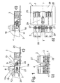
Figuren 1 - 3 ist mit dem Bezugszeichen 1 insgesamt ein Steckverbinder der nicht Teil der Erfindung ist bezeichnet, der aus einem ersten Steckverbinderteil 2 und einem zweiten Steckverbinderteil 3 besteht, wobei die beiden Steckverbinderteile 2 und 3 durch Verriegelungsschieber 4 im gekuppelten Zustand gegen unbeabsichtigtes Lösen gesichert werden können. - Im dargestellten Ausführungsbeispiel handelt es sich bei dem ersten Steckverbinderteil 2 um ein so genanntes Buchsenteil und bei dem zweiten Steckverbinderteil 3 um ein so genanntes Stecker- oder Stiftteil, wobei hier am ersten Steckverbinderteil 2, also dem Buchsenteil, ein Führungsgehäuse 5 mit einem Führungskanal 5a zur Aufnahme und verschiebbaren Führung des nur einen Verriegelungsschiebers 4 angeformt sind.
- Im zweiten Steckverbinderteil 3, also im Stiftteil, sind noch zu beschreibende konstruktive Maßnahmen ergriffen, um den relativ zum Steckverbinderteil 2 beweglichen Verriegelungsschieber 4 in einer Verriegelungsstellung fixieren zu können. Zu diesen Maßnahmen gehört ein Einführkanal bzw. Führungskanal 10 für den Verriegelungsschieber 4. Es sei an dieser Stelle ausdrücklich darauf hingewiesen, daß hier selbstverständlich auch eine Umkehr möglich ist, d. h., daß der Verriegelungsschieber 4 in entsprechenden Führungskanälen des Stiftteiles 3 geführt und das Buchsenteil 2 entsprechende Gestaltungen für die Verriegelung der Verriegelungsschieber 4 aufweist.
- Der Steckverbinder ist als Leiterplatten-Steckverbinder zur Kontaktierung einer Leiterplatte 25 ausgebildet.
- Dazu ist das eine Steckverbinderteil 3 ist auf der Leiterplatte 25 angeordnet. Es weist vier in einer Reihe angeordnete Stiftkontakte 26 auf, welche winklig ausgelegt sind mit einem ihrer Enden an der Leiterplatte 25 verlötet sind, wo sie Leiterbahnen kontaktieren, und die mit ihrem weiteren Ende einen Teil der zu kuppelnden Kontakte des Steckgesichtes des zweiten Steckverbinderteils 3 zur Kopplung mit dem Steckgesicht des anderen Steckverbinderteils 2 bilden.
- Am ersten Steckverbinderteil 2 sind dagegen Buchsenkontakte (hier nicht zu erkennen) angeordnet, welche die Kontakte 26 des zweiten Steckverbinderteils 3 im zusammengesteckten Zustand kontaktieren und welche leitend mit Anschlüssen 27, hier beispielhaft Schraubanschlüssen, zum Anschluss abgehender Leiter (hier nicht dargestellt) versehen sind. Auch die Anschlüsse 27 sind in einer Reihe angeordnet.
- Die Steckverbinderteile weisen jeweils ein Gehäuse 28, 29 auf, wobei die nur eine (dargestellt und bevorzugt) oder die zwei oder mehr (nicht dargestellt) Verriegelungen - insbesondere der Verriegelungsschieber 4 und der korrespondierende Führungskanal 5 - nicht seitlich außen neben der Reihe aus den zu koppelnden Kontakten angeordnet ist/sind sondern in der Reihe jeweils zwischen zwei der miteinander zu koppelnden Kontakten der zwei Steckverbinderteile 26 und 27.
- Diese Anordnung wird besonders gut aus den
Fig. 1a und 1b deutlich. Hier ist die Anzahl der miteinander zu verbindenden Kontakte der Steckgesichter der beiden Steckverbinderteile 2, 3 gerade. Sie beträgt beispielhaft vier. In diesem Fall bietet es sich an, die Verriegelung mit ihren Elemente 4 und 5 mittig in der Kontaktreihe aus den Kontakten 26 anzuordnen, so dass zu ihren beiden Seiten hin gleich viele - hier zwei - der Kontakte angeordnet sind. - In diesem Fall kann die Anzahl der Verriegelungen bzw. der Verriegelungsschieber 4 und Führungskanäle 5a, 10 auf jeweils nur jeweils ein einziges dieser Elemente reduziert werden, da die Verriegelung derart optimiert angeordnet ist, dass sie Kräfte, welche auf den Steckverbinder wirken können, optimal aufnimmt.
- Dies ist kein Teil der Erfindung. Sie wird durch die Erfindung optimiert.
- Nach dieser Erfindung werden im Bereich der Verriegelung weitere Funktionselemente angeordnet.
- In Hinsicht auf die Maßnahme, dem Verriegelungsschieber weitere Funktionselemente zuzuordnen, sei darauf hingewiesen, daß eine Verriegelung der beiden Steckverbinderteile 2 und 3 relativ zueinander gegebenenfalls auch mit zwei oder mehr Verriegelungsschiebern 4 durchgeführt werden kann. Dabei können dann nur einem oder auch mehreren bzw. allen Verriegelungsschiebern diese weiteren Funktionselemente, insbesondere Kontakte, zugeordnet werden. Diese weitere Ausführung kann aber auch angewendet werden, wenn zwei Verriegelungsschieber seitlich neben der Reihe der zu verbindenden Kontakte der Steckverbinderteile angeordnet sind.
- In den
Figuren 1-3 ist mit dem Bezugszeichen 6 die Kupplungsebene zwischen den beiden Steckverbinderteilen 2 und 3 bzw. deren Steckgesichtern bezeichnet. - Wie aus den Zeichnungen deutlich erkennbar, verlaufen die Führungskanäle 5a und 10 lotrecht zu der besagten Kupplungsebene 6, so daß auch entsprechend der oder die Verriegelungsschieber 4 lotrecht zur Kupplungsebene 6 verschiebbar sind.
- Jeder Verriegelungsschieber 4 ist an seinem dem zweiten Steckverbinderteil 3 zugewandten Ende mit einer mit einem Rastnocken 7 ausgestatteten, federnden Zunge 8 versehen. Der Rastvorsprung 7 ist zur freien Stirnseite der Zunge 8 hin gesehen mit einer schräg abfallenden Einlaufschräge 9 versehen.
- Der federnden Zunge 8 mit dem Rastnocken 7 liegt der Einführkanal 10 des zweiten Steckverbinderteils 3 gegenüber, durch welchen der Rastnocken 7 sowie ein Teil der federnden Zunge 8 zum Zwecke der Verriegelung der beiden Steckverbinderteile 2 und 3 in das zweite Steckverbinderteil 3 einführbar ist, bis der Rastnocken 7 eine den Führungskanal 5 endseitig umgebende Stirnfläche 11 hintergreift. Diese Position ergibt sich deutlich aus
Figur 1d . - Die federnde Zunge 8 ist angeformt an einen Betätigungsbügel 12 des Verriegelungsschiebers 4, wobei der Betätigungsbügel 12 außerhalb des jeweiligen Führungskanals 5 des ersten Steckverbinderteils 2 liegt und zur leichteren Betätigung an seiner dem Führungskanals 5 abgewandt liegenden Oberseite beispielsweise mit Rippen 13 versehen ist. Alternativ zu diesen Rippen können hier auch andere Mittel zur Verbesserung der Betätigung vorgesehen sein, beispielsweise angeformte Noppen oder dergleichen.
- Durch Druck auf den Betätigungsbügel 12 kann die federnde Zunge 8 mit dem Rastnocken 7 so weit nach unten gedrückt werden, daß der Rastnocken 7 aus seiner Verriegelungsposition heraus in eine Stellung gebracht ist, die ein Zurückschieben des Verriegelungsschiebers 4 in die Lösestellung gemäß
Figur 1c ermöglicht, wobei dieses Zurückverschieben erfolgt durch gleichzeitigen Druck auf die Betätigungsbügel 12, wie auch eine Verschiebung. Durch das Zurückverschieben kann dann der komplette Verriegelungsschieber 4 wieder in seine Lösestellung gemäßFigur 1c gebracht werden. - Im verriegelten Zustand liegt zumindest eine dem Betätigungsbügel 12 benachbarte und an dem der Kupplungsebene 6 abgewandt liegenden Ende des Verriegelungsschiebers 4 vorgesehene Anschlagnocke 17 an der Begrenzungswand 16 an.
- Dabei ist der Verschiebeweg des Verriegelungsschiebers 4 bestimmt durch die Länge der Begrenzungswand 16, an der wechselweise der Bügelabschnitt 12a und die Anschlagnocke 17 anliegen.
- Der Verriegelungsschieber 4 kann zweckmäßigerweise auch in dem der Begrenzungswand 16 gegenüberliegenden Bereich mit einer Anschlagnocke 17 versehen sein, die im verriegelten Zustand dann an einer der Begrenzungswand 16 gegenüberliegenden Seitenwand 18 des Führungsgehäuses 5 anliegt.
- Im verriegelten Zustand schließt der Verriegelungsschieber 4 mit den Stirnflächen des Führungsgehäuses 5 vorzugsweise bündig ab.
- In seinem mittleren Bereich ist der Verriegelungsschieber 4 vorzugsweise mit einer in Verschieberichtung verlaufenden Durchgangsbohrung 20 versehen.
- Diese Durchgangsbohrung 20 kann für eine optionale Verriegelungsschraube oder alternativ hier für ein weiteres elektrisches Funktionselement wie einen Kontakt 21 genutzt werden, der beim Zusammenschieben bzw. Zusammenstecken der beiden Steckverbinderteile ein weiteres Funktionselement wie einen Gegenkontakt 22 am weiteren Steckverbinderteil kontaktiert.
- Die Kontakte 21, 22 können als Buchsenkontakt und als Stiftkontakt bzw. als hier nicht dargestelltes hermaphrodites Kontaktpaar ausgebildet sein, von den der Buchsenkontakt hier beispielhaft den Kontakt 21 und der Stiftkontakt beispielhaft den Gegenkontakt 22 am weiteren Steckverbinderteil bildet (
Fig. 1 ) - Die Funktionselemente können aber auch die Elemente 23, 24 eines Reedkontaktes, bestehend magnetisch betätigten Kontakten z.B. auf der Leiterplatte oder im Bauraum eines Flansches und einem Permanentmagneten im beweglichen Teil der Verriegelungsvorrichtung oder umgekehrt ausgebildet sein (
Fig. 2 ). - Alternativ ist es auch denkbar, als Funktionselement einen Stößel am Verriegelungsschieber 4 oder den Verriegelungsschieber selbst als Stößel zu nutzen, um zwei Kontakte wie Bleche oder Stifte 14, 15 am korrespondierenden Steckverbinderteil 3 zu schließen (
Fig. 3 ) - Der Verriegelungsschieber bietet den Vorteil, dass der Verriegelungszustand optisch aus der Position des Verriegelungsschiebers 4 erkennbar ist.
- Die weiteren Funktionselemente, welche in die Verriegelung integriert sind, erlauben insbesondere eine auch elektrische Überwachung der Verriegelungsfunktion durch eine übergeordnete Steuerungs- und Überwachungsanlage. Es ist auch denkbar, den Zustand optisch oder akustisch z.B. mit einer LED direkt an dem Steckverbinder anzuzeigen. Vorteilhaft ist, dass durch die weiteren Kontakte ggf. auf separate weitere Kabelverbindungen verzichtet werden kann, da der Steckverbinder weitere integrierte Kontakte z.B. zu Steuerungszwecken bereitstellt.
- Denkbar ist es auch, z.B. durch eine Mehrfachbestückung mindestens einer Kontaktkammer mit mindestens zwei elektrisch voneinander getrennten Hilfskontakten den wenigstens einen oder die weiteren (Hilfs-)Kontakte für andere Zwecke zu nutzen, so als Steuerkontakte oder als Kontakte für eine Daten- oder Versorgungsleitung z.B. eines Busses, zu dem auch die weiteren zu verbindenden an den Steckverbinderteilen gehören (an den Steckverbinderteilen werden dann ggf,. weitere Anschlüsse zur Leiterplatte bzw. nach außen hin ausgebildet, die in beliebiger Technik wie Push-In oder dgl. ausgelegt sein können).
- Der Verriegelungsschieber 4 ist hier beispielhaft einstückig aus einem federelastischen Material, vorzugsweise aus Kunststoff, hergestellt.
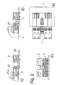
- Nach
Fig. 4 wird mit dem Bezugszeichen 1 wiederum der Steckverbinder bezeichnet, der aus dem ersten Steckverbinderteil 2 und dem zweiten Steckverbinderteil 3 besteht, wobei die beiden Steckverbinderteile 2 und 3 durch eine Verriegelungsvorrichtung 4 im gekuppelten Zustand gegen unbeabsichtigtes Lösen gesichert werden können. - Die Verriegelungsvorrichtung 4 der
Fig. 4 sichert auch wiederum in einer Verriegelungsstellung (Fig 4c ) die beiden miteinander gekuppelten Steckverbinderteile 2, 3 gegen unbeabsichtigtes Lösen und ist in eine Haltevorrichtung des zweiten Steckverbinderteils 3 beweglich. Die Haltevorrichtung ist als Rastkante 30 im Einführkanal 10 ausgebildet. Die Verriegelungsvorrichtung 4 ist am ersten Steckverbinderteil vorzugsweise zwischen zwei der Kontakte nicht relativ zu diesem Steckverbinderteil 2 verschieblich sondern an diesem schwenkbar angeordnet. Sie weist wiederum eine Zunge 8 auf, an deren freiem Ende ein Rasthaken bzw. Rastnocken 7 ausgebildet ist, der auch wiederum vorzugsweise eine Einlaufschräge 9 aufweist. - Die Zunge 8 ist ferner in einem vom Rasthaken beabstandet liegenden Bereich über einen Steg 31 mit dem zweiten Steckverbinderteil 2 verbunden. An die Zunge 8 ist ferner ein Betätigungsbügel 12 angeformt, der derart ausgestaltet und angeordnet ist, dass durch Druck auf den Betätigungsbügel 12 senkrecht zur Steckrichtung X die Zunge 8 mit dem Rasthaken/-nocken 7 im wesentlichen senkrecht zur Steckrichtung X beweglich bzw. verschwenkbar ist.
- Beim Zusammenschieben der beiden Steckverbinderteile 2, 3 (
Fig. 4a ) berührt die Einlaufschräge 9 zunächst die Rastkante 30, wodurch die Zunge 8 ausgelenkt wird (Fig. 4d ), bis der Rastnocken 7 beim weiteren Zusammenschieben der beiden Steckverbinderteile 2, 3 die Rastkante 30 schließlich rastend hintergreift. In dieser Stellung sind die beiden Steckverbinderteile 2, 3 gegen ein unbeabsichtigtes Auseinanderziehen gesichert (Fig. 4c ). - Durch Druck auf den Betätigungsbügel 12 kann (entsprechend zu
Fig. 4b ) die Zunge 8 mit dem Rastnocken 7 aus der Verriegelungsstellung herausgeschwenkt werden, so dass die beiden Steckverbinderteile 2, 3 wieder auseinander gezogen werden können. - Die weiteren optionalen Funktionen der vorstehenden Figuren sind auch bei diesem Ausführungsbeispiel realisierbar.
-
- Steckverbinder
- 1
- Steckverbinderteil
- 2
- Steckverbinderteil
- 3
- Verriegelungsschieber
- 4
- Führungsgehäuse
- 5
- Führungskanal
- 5a
- Kupplungsebene
- 6
- Rastnocken
- 7
- Zunge
- 8
- Einlaufschräge
- 9
- Einführkanal
- 10
- Stirnfläche
- 11
- Betätigungsbügel
- 12
- Rippen
- 13
- Bleche
- 14, 15
- Anschlagnocke
- 17
- Begrenzungswand
- 16
- Seitenwand
- 18
- Durchgangsbohrung
- 20
- Kontakt
- 21
- Gegenkontakt
- 22
- Elemente
- 23,24
- Leiterplatte
- 25
- Stiftkontakte
- 26
- Anschlüsse
- 27
- Gehäuse
- 28, 29
- Rastkante
- 30
- Steg
- 31
Claims (14)
- Steckverbinder (1), insbesondere Leiterplatten-Steckverbinder, mita) einem ersten Steckverbinderteil (2) und einem zweiten Steckverbinderteil (3), wobei das eine der Steckverbinderteile vorzugsweise ein Buchsenteil und das andere der Steckverbinderteile vorzugsweise ein Stiftteil ist,b) sowie mit mindestens einer Verriegelungsvorrichtung (4), welche in einer Verriegelungsstellung die beiden miteinander gekuppelten Steckverbinderteile (2, 3) gegen unbeabsichtigtes Lösen sichert und die in eine Haltevorrichtung des zweiten Steckverbinderteils (3) beweglich, insbesondere verschiebbar und/oder verschwenkbar ist,c) wobei die Steckverbinderteile (2, 3) jeweils mehrere vorzugsweise in wenigstens einer Reihe angeordnete, miteinander zu verbindende Kontakte im Bereich ihrer Steckgesichter aufweisen,d) die Verriegelungsvorrichtung und die Haltevorrichtung in der wenigstens einen Reihe der miteinander zu verbindenden Kontakte jeweils zwischen zweien der Kontakte angeordnet ist,
dadurch gekennzeichnet, dasse) die Verriegelungsvorrichtung am ersten Steckverbinderteil schwenkbar angeordnet ist,f) die Verriegelungsvorrichtung einen relativ zum ersten Steckverbinderteil (2) verschwenkbaren Rastnocken (7) aufweist, der beim Zusammenschieben der beiden Steckverbinderteile rastend am zweiten Steckverbinderteil (3) arretiert wird, und dassg) die Verriegelungsvorrichtung eine Zunge (8) aufweist, an deren freiem Ende der Rasthaken bzw. Rastnocken (7) ausgebildet ist, der eine Einlaufschräge (9) aufweist, wobei die Zunge (8) in einem vom Rasthaken beabstandet liegenden Bereich über einen Steg (31) mit dem zweiten Steckverbinderteil (2) verbunden ist undh) wobei an die Zunge (8) ein Betätigungsbügel (12) angeformt ist, der derart ausgestaltet und angeordnet ist, dass durch Druck auf den Betätigungsbügel (12) senkrecht zur Steckrichtung (X) die Zunge mit dem Rastnocken (7) im wesentlichen senkrecht zur Steckrichtung verschwenkbar ist. - Steckverbinder (1) nach Anspruch 1, dadurch gekennzeichnet, dass im Bereich der wenigstens einen Verriegelungsvorrichtung und/oder der Haltevorrichtung weitere, zueinander korrespondierende Funktionselemente angeordnet sind.
- Steckverbinder nach Anspruch 1 oder 2, dadurch gekennzeichnet, dass die Verriegelungsvorrichtung (4) und/oder eines der weiteren Funktionselemente zwischen zweien der beiden Kontakte derart angeordnet ist, dass sie/es die Linie (L) unterbricht, welche die beiden zur Verriegelungsvorrichtung benachbarten Kontakte unmittelbar miteinander verbindet.
- Steckverbinder (1) nach Anspruch 2 oder 3, dadurch gekennzeichnet, dass in der Verriegelungsvorrichtung und/oder der Haltevorrichtung die weiteren, zueinander korrespondierenden Funktionselemente angeordnet sind.
- Steckverbinder (1) nach Anspruch 2, 3 oder 4, dadurch gekennzeichnet, dass im Bereich der Verriegelungsvorrichtung und/oder wenigstens eines zugehörigen Einführkanals als der Haltevorrichtung weitere, zueinander korrespondierende Funktionselemente angeordnet sind.
- Steckverbinder nach Anspruch 2, 3, 4 oder 5, dadurch gekennzeichnet, dass die weiteren Funktionselemente je Steckverbinderteil als einer oder mehrere weitere elektrisch leitende Kontakte (21, 22) ausgebildet sind.
- Steckverbinder nach Anspruch 2, 3, 4 oder 5, dadurch gekennzeichnet, dass die weiteren Funktionselemente als Bauelemente (23, 24) eines Reedkontaktes ausgebildet sind.
- Steckverbinder nach Anspruch 2, 3, 4 oder 5, dadurch gekennzeichnet, dass die weiteren Funktionselemente als lichtleitende Kontakte ausgebildet sind.
- Steckverbinder nach Anspruch 2, 3, 4 oder 5, dadurch gekennzeichnet, dass die weiteren Funktionselemente zwei leitende Kontakte (14, 15) an dem einen der Steckverbinderteile (3) umfassen, welche durch den Verriegelungsvorrichtung (4) oder ein Element am Verriegelungsvorrichtung (4) beim Zusammenstecken der beiden Steckverbinderteile miteinander verbunden werden.
- Steckverbinder nach einem der vorstehenden Ansprüche, dadurch gekennzeichnet, dass eines der Funktionselemente in einer Durchgangsbohrung (20) im Verriegelungsvorrichtung (4) angeordnet ist.
- Steckverbinder nach einem der vorstehenden Ansprüche 2 bis 8, dadurch gekennzeichnet, dass eines der Funktionselemente in einem Einführkanal (10) des zweiten Steckverbinderteils (3) angeordnet ist.
- Steckverbinder nach einem der Ansprüche 2 bis 11, dadurch gekennzeichnet, dass die weiteren Funktionselemente als elektromechanisch wirkende Elemente ausgebildet sind.
- Steckverbinder nach einem der Ansprüche 2 bis 11, dadurch gekennzeichnet, dass die weiteren Funktionselemente als elektromagnetisch wirkende Elemente ausgebildet sind.
- Steckverbinder nach einem der vorstehenden Ansprüche, dadurch gekennzeichnet, dass elektromechanisch (magnetisch / induktiv oder thermo-eleklrisch) bewegbare Elemente vorgesehen sind, die derart betätigbar sind, dass ein Lösen der Verriegelung während dieser Betätigungsdauer nicht möglich ist bzw. wirksam verhindert wird.
Applications Claiming Priority (1)
| Application Number | Priority Date | Filing Date | Title |
|---|---|---|---|
| DE202007005300U DE202007005300U1 (de) | 2007-04-11 | 2007-04-11 | Steckverbinder, insbesondere für Leiterplatten |
Publications (3)
| Publication Number | Publication Date |
|---|---|
| EP1981127A2 EP1981127A2 (de) | 2008-10-15 |
| EP1981127A3 EP1981127A3 (de) | 2009-12-23 |
| EP1981127B1 true EP1981127B1 (de) | 2015-09-09 |
Family
ID=39564224
Family Applications (1)
| Application Number | Title | Priority Date | Filing Date |
|---|---|---|---|
| EP08102529.8A Active EP1981127B1 (de) | 2007-04-11 | 2008-03-12 | Steckverbinder, insbesondere für Leiterplatten |
Country Status (5)
| Country | Link |
|---|---|
| US (1) | US7651362B2 (de) |
| EP (1) | EP1981127B1 (de) |
| JP (1) | JP2008277292A (de) |
| CN (1) | CN101286603B (de) |
| DE (1) | DE202007005300U1 (de) |
Families Citing this family (11)
| Publication number | Priority date | Publication date | Assignee | Title |
|---|---|---|---|---|
| DE202009002159U1 (de) | 2009-02-14 | 2010-07-15 | Weidmüller Interface GmbH & Co. KG | Steckverbinder, insbesondere für Leiterplatten |
| DE102013114739A1 (de) * | 2013-12-20 | 2015-06-25 | Endress + Hauser Gmbh + Co. Kg | Steckverbindungssystem |
| DE102019104558C5 (de) * | 2019-02-22 | 2025-07-03 | Phoenix Contact Gmbh & Co. Kg | Steckverbinderteil mit einer Rasteinrichtung |
| DE102020125381A1 (de) * | 2020-09-29 | 2022-03-31 | Harting Electric Gmbh & Co. Kg | Befestigungssystem für Steckverbinder |
| CN114824858B (zh) * | 2021-01-29 | 2025-11-28 | 康哲电脑配件(吴江)有限公司 | 用于电子装置的固定器 |
| DE102021115690A1 (de) | 2021-06-17 | 2022-12-22 | Phoenix Contact Gmbh & Co. Kg | Steckverbinder mit Verriegelungselement |
| DE102021115691A1 (de) | 2021-06-17 | 2022-12-22 | Phoenix Contact Gmbh & Co. Kg | Variabel positionierbare Rastlasche und Steckverbinder |
| LU500296B1 (de) | 2021-06-17 | 2022-12-20 | Phoenix Contact Gmbh & Co | Variabel positionierbare Rastlasche und Steckverbinder |
| LU500295B1 (de) | 2021-06-17 | 2022-12-19 | Phoenix Contact Gmbh & Co | Steckverbinder mit Verriegelungselement |
| US11848517B2 (en) | 2022-04-11 | 2023-12-19 | Dinkle Enterprise Co., Ltd. | Terminal block structure and unbuckling unit thereof |
| DE102022112023B3 (de) | 2022-05-13 | 2023-07-20 | Dinkle Electric Machinery (China) Co., Ltd. | Anschlussblockstruktur mit Entkopplungseinheit |
Family Cites Families (21)
| Publication number | Priority date | Publication date | Assignee | Title |
|---|---|---|---|---|
| US3792208A (en) * | 1972-11-15 | 1974-02-12 | Control Data Corp | Communications connector apparatus utilizing radiant energy |
| DE3112078C2 (de) * | 1981-03-27 | 1985-12-19 | Richard Hirschmann Radiotechnisches Werk, 7300 Esslingen | Hybrid-Steckverbindung für optische und elektrische Leiter |
| JPS60183380U (ja) * | 1984-05-17 | 1985-12-05 | アムプ インコ−ポレ−テッド | 電気接続子ハウジング |
| DE3440043C2 (de) * | 1984-11-02 | 1986-10-02 | F. Wieland, Elektrische Industrie GmbH, 8600 Bamberg | Elektrische Steckverbindung |
| DE9311457U1 (de) * | 1993-07-31 | 1993-10-07 | Harting Elektronik Gmbh, 32339 Espelkamp | Steckverbinder mit Rastmitteln |
| US5411402A (en) * | 1993-12-17 | 1995-05-02 | Itt Corporation | Connector assembly for IC card |
| US5618201A (en) * | 1994-06-14 | 1997-04-08 | Yazaki Corporation | Connector having engagement detecting device |
| DE19535836C2 (de) | 1995-09-26 | 2003-10-30 | Grote & Hartmann | Rasteinrichtung, insbesondere für elektrische Steckverbindergehäuse |
| US5538437A (en) * | 1995-03-03 | 1996-07-23 | Itt Industries, Inc. | Connector assembly for IC card |
| US5554045A (en) * | 1995-06-19 | 1996-09-10 | Itt Cannon, Inc. | Latch for IC card connector |
| DE29513997U1 (de) * | 1995-08-31 | 1995-12-07 | HTS-Elektrotechnik GmbH, 53819 Neunkirchen-Seelscheid | Vorrichtung zur Verriegelung von Steckergehäusen |
| JP3521772B2 (ja) * | 1998-11-26 | 2004-04-19 | 住友電装株式会社 | コネクタ |
| US6146180A (en) * | 1999-11-12 | 2000-11-14 | Itt Manufacturing Enterprises, Inc. | Connector latch with integrated auxiliary contacts |
| JP3405954B2 (ja) * | 2000-03-13 | 2003-05-12 | 日本圧着端子製造株式会社 | コネクタのロック構造 |
| JP2003187910A (ja) * | 2001-12-13 | 2003-07-04 | Sumitomo Wiring Syst Ltd | コネクタ |
| DE20201609U1 (de) | 2002-02-01 | 2003-06-18 | Weidmüller Interface GmbH & Co., 32760 Detmold | Steckverbinder |
| JP4293887B2 (ja) * | 2003-11-19 | 2009-07-08 | イリソ電子工業株式会社 | コネクタ |
| JP2005190821A (ja) * | 2003-12-25 | 2005-07-14 | Sumitomo Wiring Syst Ltd | コネクタ装置 |
| TWI278151B (en) * | 2005-04-29 | 2007-04-01 | Hon Hai Prec Ind Co Ltd | Cable connector assembly |
| US7074070B1 (en) * | 2005-06-17 | 2006-07-11 | Cheng Uei Precision Industry Co., Ltd. | Connector assembly with latch mechanism |
| JP4606283B2 (ja) * | 2005-09-12 | 2011-01-05 | 矢崎総業株式会社 | コネクタ |
-
2007
- 2007-04-11 DE DE202007005300U patent/DE202007005300U1/de not_active Expired - Lifetime
-
2008
- 2008-03-12 EP EP08102529.8A patent/EP1981127B1/de active Active
- 2008-04-07 US US12/080,890 patent/US7651362B2/en active Active
- 2008-04-09 JP JP2008101540A patent/JP2008277292A/ja active Pending
- 2008-04-10 CN CN2008100919415A patent/CN101286603B/zh active Active
Also Published As
| Publication number | Publication date |
|---|---|
| CN101286603A (zh) | 2008-10-15 |
| DE202007005300U1 (de) | 2008-08-21 |
| US20090117756A1 (en) | 2009-05-07 |
| US7651362B2 (en) | 2010-01-26 |
| JP2008277292A (ja) | 2008-11-13 |
| EP1981127A2 (de) | 2008-10-15 |
| EP1981127A3 (de) | 2009-12-23 |
| CN101286603B (zh) | 2012-03-28 |
Similar Documents
| Publication | Publication Date | Title |
|---|---|---|
| EP1981127B1 (de) | Steckverbinder, insbesondere für Leiterplatten | |
| DE60027611T2 (de) | Kabelverbinder mit gesteuerter Impedanz | |
| DE69320263T2 (de) | Auswurfvorrichtung in einer Verbindervorrichtung für IC-Karten | |
| DE19920981C2 (de) | Elektrischer Verbinder | |
| EP2526591B1 (de) | Steckerelement mit einem verriegelungsmechanismus | |
| DE10203162B4 (de) | Verbinder | |
| EP0899818B1 (de) | Elektrische Anschlussklemme, insbesondere für den Einsatz auf Leiterplatten | |
| EP0805366A1 (de) | Steckverbindung | |
| DE202019105075U1 (de) | Anschlussklemme für Leiter | |
| DE19813458A1 (de) | Elektrischer Verbinder | |
| DE102014106277B4 (de) | Ein Elektronikgehäuse mit einer Anschlussleiste für ein Elektronikgerät | |
| DE69825667T2 (de) | Verriegelung für Smartcard-Adapter | |
| DE3522067C2 (de) | ||
| DE19511508C2 (de) | Elektrischer Leiterplattenverbinder | |
| DE3318137C2 (de) | Mehrpolige elektrische Steckvorrichtung | |
| EP3493333B1 (de) | Elektrische steckverbindung zur datenübertragung | |
| EP0935269B1 (de) | Schaltergehäuse für elektrischen Schalter | |
| EP3782235A1 (de) | Direktsteckverbinder | |
| DE102013111577A1 (de) | Elektronikgerät | |
| DE10204842B4 (de) | Leiterplattensteckverbinder | |
| EP1595311B1 (de) | Steckverbindung | |
| DE3127246C2 (de) | ||
| DE29607793U1 (de) | Steckverbindung | |
| DE2714409C3 (de) | Verriegelungsvorrichtung für eine Steckvorrichtung | |
| DE19709198A1 (de) | Steckeranordnung mit einem Betätigungsschieber |
Legal Events
| Date | Code | Title | Description |
|---|---|---|---|
| PUAI | Public reference made under article 153(3) epc to a published international application that has entered the european phase |
Free format text: ORIGINAL CODE: 0009012 |
|
| AK | Designated contracting states |
Kind code of ref document: A2 Designated state(s): AT BE BG CH CY CZ DE DK EE ES FI FR GB GR HR HU IE IS IT LI LT LU LV MC MT NL NO PL PT RO SE SI SK TR |
|
| AX | Request for extension of the european patent |
Extension state: AL BA MK RS |
|
| RIC1 | Information provided on ipc code assigned before grant |
Ipc: H01R 13/641 20060101ALI20090925BHEP Ipc: H01R 13/639 20060101ALI20090925BHEP Ipc: H01R 13/627 20060101AFI20080707BHEP |
|
| PUAL | Search report despatched |
Free format text: ORIGINAL CODE: 0009013 |
|
| AK | Designated contracting states |
Kind code of ref document: A3 Designated state(s): AT BE BG CH CY CZ DE DK EE ES FI FR GB GR HR HU IE IS IT LI LT LU LV MC MT NL NO PL PT RO SE SI SK TR |
|
| AX | Request for extension of the european patent |
Extension state: AL BA MK RS |
|
| 17P | Request for examination filed |
Effective date: 20100310 |
|
| 17Q | First examination report despatched |
Effective date: 20100521 |
|
| AKX | Designation fees paid |
Designated state(s): AT BE BG CH CY CZ DE DK EE ES FI FR GB GR HR HU IE IS IT LI LT LU LV MC MT NL NO PL PT RO SE SI SK TR |
|
| GRAP | Despatch of communication of intention to grant a patent |
Free format text: ORIGINAL CODE: EPIDOSNIGR1 |
|
| RIC1 | Information provided on ipc code assigned before grant |
Ipc: H01R 13/703 20060101ALI20150429BHEP Ipc: H01R 13/627 20060101AFI20150429BHEP Ipc: H01R 13/717 20060101ALI20150429BHEP Ipc: H01R 13/641 20060101ALI20150429BHEP Ipc: H01R 13/639 20060101ALI20150429BHEP |
|
| INTG | Intention to grant announced |
Effective date: 20150515 |
|
| GRAS | Grant fee paid |
Free format text: ORIGINAL CODE: EPIDOSNIGR3 |
|
| GRAA | (expected) grant |
Free format text: ORIGINAL CODE: 0009210 |
|
| AK | Designated contracting states |
Kind code of ref document: B1 Designated state(s): AT BE BG CH CY CZ DE DK EE ES FI FR GB GR HR HU IE IS IT LI LT LU LV MC MT NL NO PL PT RO SE SI SK TR |
|
| REG | Reference to a national code |
Ref country code: GB Ref legal event code: FG4D Free format text: NOT ENGLISH |
|
| REG | Reference to a national code |
Ref country code: AT Ref legal event code: REF Ref document number: 748811 Country of ref document: AT Kind code of ref document: T Effective date: 20150915 Ref country code: CH Ref legal event code: EP |
|
| REG | Reference to a national code |
Ref country code: IE Ref legal event code: FG4D Free format text: LANGUAGE OF EP DOCUMENT: GERMAN |
|
| REG | Reference to a national code |
Ref country code: DE Ref legal event code: R096 Ref document number: 502008013353 Country of ref document: DE |
|
| REG | Reference to a national code |
Ref country code: NL Ref legal event code: MP Effective date: 20150909 |
|
| PG25 | Lapsed in a contracting state [announced via postgrant information from national office to epo] |
Ref country code: LT Free format text: LAPSE BECAUSE OF FAILURE TO SUBMIT A TRANSLATION OF THE DESCRIPTION OR TO PAY THE FEE WITHIN THE PRESCRIBED TIME-LIMIT Effective date: 20150909 Ref country code: NO Free format text: LAPSE BECAUSE OF FAILURE TO SUBMIT A TRANSLATION OF THE DESCRIPTION OR TO PAY THE FEE WITHIN THE PRESCRIBED TIME-LIMIT Effective date: 20151209 Ref country code: GR Free format text: LAPSE BECAUSE OF FAILURE TO SUBMIT A TRANSLATION OF THE DESCRIPTION OR TO PAY THE FEE WITHIN THE PRESCRIBED TIME-LIMIT Effective date: 20151210 Ref country code: LV Free format text: LAPSE BECAUSE OF FAILURE TO SUBMIT A TRANSLATION OF THE DESCRIPTION OR TO PAY THE FEE WITHIN THE PRESCRIBED TIME-LIMIT Effective date: 20150909 |
|
| REG | Reference to a national code |
Ref country code: LT Ref legal event code: MG4D |
|
| PG25 | Lapsed in a contracting state [announced via postgrant information from national office to epo] |
Ref country code: ES Free format text: LAPSE BECAUSE OF FAILURE TO SUBMIT A TRANSLATION OF THE DESCRIPTION OR TO PAY THE FEE WITHIN THE PRESCRIBED TIME-LIMIT Effective date: 20150909 Ref country code: SE Free format text: LAPSE BECAUSE OF FAILURE TO SUBMIT A TRANSLATION OF THE DESCRIPTION OR TO PAY THE FEE WITHIN THE PRESCRIBED TIME-LIMIT Effective date: 20150909 Ref country code: HR Free format text: LAPSE BECAUSE OF FAILURE TO SUBMIT A TRANSLATION OF THE DESCRIPTION OR TO PAY THE FEE WITHIN THE PRESCRIBED TIME-LIMIT Effective date: 20150909 |
|
| REG | Reference to a national code |
Ref country code: FR Ref legal event code: PLFP Year of fee payment: 9 |
|
| PG25 | Lapsed in a contracting state [announced via postgrant information from national office to epo] |
Ref country code: NL Free format text: LAPSE BECAUSE OF FAILURE TO SUBMIT A TRANSLATION OF THE DESCRIPTION OR TO PAY THE FEE WITHIN THE PRESCRIBED TIME-LIMIT Effective date: 20150909 |
|
| PG25 | Lapsed in a contracting state [announced via postgrant information from national office to epo] |
Ref country code: SK Free format text: LAPSE BECAUSE OF FAILURE TO SUBMIT A TRANSLATION OF THE DESCRIPTION OR TO PAY THE FEE WITHIN THE PRESCRIBED TIME-LIMIT Effective date: 20150909 Ref country code: IS Free format text: LAPSE BECAUSE OF FAILURE TO SUBMIT A TRANSLATION OF THE DESCRIPTION OR TO PAY THE FEE WITHIN THE PRESCRIBED TIME-LIMIT Effective date: 20160109 Ref country code: EE Free format text: LAPSE BECAUSE OF FAILURE TO SUBMIT A TRANSLATION OF THE DESCRIPTION OR TO PAY THE FEE WITHIN THE PRESCRIBED TIME-LIMIT Effective date: 20150909 Ref country code: CZ Free format text: LAPSE BECAUSE OF FAILURE TO SUBMIT A TRANSLATION OF THE DESCRIPTION OR TO PAY THE FEE WITHIN THE PRESCRIBED TIME-LIMIT Effective date: 20150909 |
|
| PG25 | Lapsed in a contracting state [announced via postgrant information from national office to epo] |
Ref country code: PL Free format text: LAPSE BECAUSE OF FAILURE TO SUBMIT A TRANSLATION OF THE DESCRIPTION OR TO PAY THE FEE WITHIN THE PRESCRIBED TIME-LIMIT Effective date: 20150909 Ref country code: RO Free format text: LAPSE BECAUSE OF FAILURE TO SUBMIT A TRANSLATION OF THE DESCRIPTION OR TO PAY THE FEE WITHIN THE PRESCRIBED TIME-LIMIT Effective date: 20150909 Ref country code: PT Free format text: LAPSE BECAUSE OF FAILURE TO SUBMIT A TRANSLATION OF THE DESCRIPTION OR TO PAY THE FEE WITHIN THE PRESCRIBED TIME-LIMIT Effective date: 20160111 |
|
| PGFP | Annual fee paid to national office [announced via postgrant information from national office to epo] |
Ref country code: FI Payment date: 20160311 Year of fee payment: 9 Ref country code: FR Payment date: 20160321 Year of fee payment: 9 Ref country code: GB Payment date: 20160321 Year of fee payment: 9 |
|
| REG | Reference to a national code |
Ref country code: DE Ref legal event code: R097 Ref document number: 502008013353 Country of ref document: DE |
|
| PLBE | No opposition filed within time limit |
Free format text: ORIGINAL CODE: 0009261 |
|
| STAA | Information on the status of an ep patent application or granted ep patent |
Free format text: STATUS: NO OPPOSITION FILED WITHIN TIME LIMIT |
|
| 26N | No opposition filed |
Effective date: 20160610 |
|
| PG25 | Lapsed in a contracting state [announced via postgrant information from national office to epo] |
Ref country code: DK Free format text: LAPSE BECAUSE OF FAILURE TO SUBMIT A TRANSLATION OF THE DESCRIPTION OR TO PAY THE FEE WITHIN THE PRESCRIBED TIME-LIMIT Effective date: 20150909 Ref country code: SI Free format text: LAPSE BECAUSE OF FAILURE TO SUBMIT A TRANSLATION OF THE DESCRIPTION OR TO PAY THE FEE WITHIN THE PRESCRIBED TIME-LIMIT Effective date: 20150909 Ref country code: BE Free format text: LAPSE BECAUSE OF NON-PAYMENT OF DUE FEES Effective date: 20160331 |
|
| PG25 | Lapsed in a contracting state [announced via postgrant information from national office to epo] |
Ref country code: LU Free format text: LAPSE BECAUSE OF FAILURE TO SUBMIT A TRANSLATION OF THE DESCRIPTION OR TO PAY THE FEE WITHIN THE PRESCRIBED TIME-LIMIT Effective date: 20160312 Ref country code: MC Free format text: LAPSE BECAUSE OF FAILURE TO SUBMIT A TRANSLATION OF THE DESCRIPTION OR TO PAY THE FEE WITHIN THE PRESCRIBED TIME-LIMIT Effective date: 20150909 |
|
| REG | Reference to a national code |
Ref country code: CH Ref legal event code: PL |
|
| REG | Reference to a national code |
Ref country code: IE Ref legal event code: MM4A |
|
| PG25 | Lapsed in a contracting state [announced via postgrant information from national office to epo] |
Ref country code: IE Free format text: LAPSE BECAUSE OF NON-PAYMENT OF DUE FEES Effective date: 20160312 Ref country code: LI Free format text: LAPSE BECAUSE OF NON-PAYMENT OF DUE FEES Effective date: 20160331 Ref country code: CH Free format text: LAPSE BECAUSE OF NON-PAYMENT OF DUE FEES Effective date: 20160331 |
|
| REG | Reference to a national code |
Ref country code: AT Ref legal event code: MM01 Ref document number: 748811 Country of ref document: AT Kind code of ref document: T Effective date: 20160312 |
|
| PG25 | Lapsed in a contracting state [announced via postgrant information from national office to epo] |
Ref country code: AT Free format text: LAPSE BECAUSE OF NON-PAYMENT OF DUE FEES Effective date: 20160312 Ref country code: MT Free format text: LAPSE BECAUSE OF FAILURE TO SUBMIT A TRANSLATION OF THE DESCRIPTION OR TO PAY THE FEE WITHIN THE PRESCRIBED TIME-LIMIT Effective date: 20150909 |
|
| PGFP | Annual fee paid to national office [announced via postgrant information from national office to epo] |
Ref country code: IT Payment date: 20170323 Year of fee payment: 10 |
|
| PG25 | Lapsed in a contracting state [announced via postgrant information from national office to epo] |
Ref country code: FI Free format text: LAPSE BECAUSE OF NON-PAYMENT OF DUE FEES Effective date: 20170312 |
|
| GBPC | Gb: european patent ceased through non-payment of renewal fee |
Effective date: 20170312 |
|
| REG | Reference to a national code |
Ref country code: FR Ref legal event code: ST Effective date: 20171130 |
|
| PG25 | Lapsed in a contracting state [announced via postgrant information from national office to epo] |
Ref country code: FR Free format text: LAPSE BECAUSE OF NON-PAYMENT OF DUE FEES Effective date: 20170331 |
|
| PG25 | Lapsed in a contracting state [announced via postgrant information from national office to epo] |
Ref country code: GB Free format text: LAPSE BECAUSE OF NON-PAYMENT OF DUE FEES Effective date: 20170312 |
|
| PG25 | Lapsed in a contracting state [announced via postgrant information from national office to epo] |
Ref country code: CY Free format text: LAPSE BECAUSE OF FAILURE TO SUBMIT A TRANSLATION OF THE DESCRIPTION OR TO PAY THE FEE WITHIN THE PRESCRIBED TIME-LIMIT Effective date: 20150909 Ref country code: HU Free format text: LAPSE BECAUSE OF FAILURE TO SUBMIT A TRANSLATION OF THE DESCRIPTION OR TO PAY THE FEE WITHIN THE PRESCRIBED TIME-LIMIT; INVALID AB INITIO Effective date: 20080312 |
|
| PG25 | Lapsed in a contracting state [announced via postgrant information from national office to epo] |
Ref country code: TR Free format text: LAPSE BECAUSE OF FAILURE TO SUBMIT A TRANSLATION OF THE DESCRIPTION OR TO PAY THE FEE WITHIN THE PRESCRIBED TIME-LIMIT Effective date: 20150909 |
|
| PG25 | Lapsed in a contracting state [announced via postgrant information from national office to epo] |
Ref country code: BG Free format text: LAPSE BECAUSE OF FAILURE TO SUBMIT A TRANSLATION OF THE DESCRIPTION OR TO PAY THE FEE WITHIN THE PRESCRIBED TIME-LIMIT Effective date: 20150909 |
|
| PG25 | Lapsed in a contracting state [announced via postgrant information from national office to epo] |
Ref country code: IT Free format text: LAPSE BECAUSE OF NON-PAYMENT OF DUE FEES Effective date: 20180312 |
|
| P01 | Opt-out of the competence of the unified patent court (upc) registered |
Effective date: 20230524 |
|
| PGFP | Annual fee paid to national office [announced via postgrant information from national office to epo] |
Ref country code: DE Payment date: 20260319 Year of fee payment: 19 |