EP1978400B1 - Beschichtete struktur und elektrode für eine elektrische schaltung damit - Google Patents
Beschichtete struktur und elektrode für eine elektrische schaltung damit Download PDFInfo
- Publication number
- EP1978400B1 EP1978400B1 EP07706824A EP07706824A EP1978400B1 EP 1978400 B1 EP1978400 B1 EP 1978400B1 EP 07706824 A EP07706824 A EP 07706824A EP 07706824 A EP07706824 A EP 07706824A EP 1978400 B1 EP1978400 B1 EP 1978400B1
- Authority
- EP
- European Patent Office
- Prior art keywords
- thin film
- ito
- film
- molybdenum
- multilayer structure
- Prior art date
- Legal status (The legal status is an assumption and is not a legal conclusion. Google has not performed a legal analysis and makes no representation as to the accuracy of the status listed.)
- Not-in-force
Links
Images

Classifications
-
- C—CHEMISTRY; METALLURGY
- C23—COATING METALLIC MATERIAL; COATING MATERIAL WITH METALLIC MATERIAL; CHEMICAL SURFACE TREATMENT; DIFFUSION TREATMENT OF METALLIC MATERIAL; COATING BY VACUUM EVAPORATION, BY SPUTTERING, BY ION IMPLANTATION OR BY CHEMICAL VAPOUR DEPOSITION, IN GENERAL; INHIBITING CORROSION OF METALLIC MATERIAL OR INCRUSTATION IN GENERAL
- C23C—COATING METALLIC MATERIAL; COATING MATERIAL WITH METALLIC MATERIAL; SURFACE TREATMENT OF METALLIC MATERIAL BY DIFFUSION INTO THE SURFACE, BY CHEMICAL CONVERSION OR SUBSTITUTION; COATING BY VACUUM EVAPORATION, BY SPUTTERING, BY ION IMPLANTATION OR BY CHEMICAL VAPOUR DEPOSITION, IN GENERAL
- C23C14/00—Coating by vacuum evaporation, by sputtering or by ion implantation of the coating forming material
- C23C14/06—Coating by vacuum evaporation, by sputtering or by ion implantation of the coating forming material characterised by the coating material
- C23C14/08—Oxides
- C23C14/086—Oxides of zinc, germanium, cadmium, indium, tin, thallium or bismuth
-
- C—CHEMISTRY; METALLURGY
- C23—COATING METALLIC MATERIAL; COATING MATERIAL WITH METALLIC MATERIAL; CHEMICAL SURFACE TREATMENT; DIFFUSION TREATMENT OF METALLIC MATERIAL; COATING BY VACUUM EVAPORATION, BY SPUTTERING, BY ION IMPLANTATION OR BY CHEMICAL VAPOUR DEPOSITION, IN GENERAL; INHIBITING CORROSION OF METALLIC MATERIAL OR INCRUSTATION IN GENERAL
- C23C—COATING METALLIC MATERIAL; COATING MATERIAL WITH METALLIC MATERIAL; SURFACE TREATMENT OF METALLIC MATERIAL BY DIFFUSION INTO THE SURFACE, BY CHEMICAL CONVERSION OR SUBSTITUTION; COATING BY VACUUM EVAPORATION, BY SPUTTERING, BY ION IMPLANTATION OR BY CHEMICAL VAPOUR DEPOSITION, IN GENERAL
- C23C14/00—Coating by vacuum evaporation, by sputtering or by ion implantation of the coating forming material
- C23C14/06—Coating by vacuum evaporation, by sputtering or by ion implantation of the coating forming material characterised by the coating material
- C23C14/08—Oxides
-
- C—CHEMISTRY; METALLURGY
- C23—COATING METALLIC MATERIAL; COATING MATERIAL WITH METALLIC MATERIAL; CHEMICAL SURFACE TREATMENT; DIFFUSION TREATMENT OF METALLIC MATERIAL; COATING BY VACUUM EVAPORATION, BY SPUTTERING, BY ION IMPLANTATION OR BY CHEMICAL VAPOUR DEPOSITION, IN GENERAL; INHIBITING CORROSION OF METALLIC MATERIAL OR INCRUSTATION IN GENERAL
- C23C—COATING METALLIC MATERIAL; COATING MATERIAL WITH METALLIC MATERIAL; SURFACE TREATMENT OF METALLIC MATERIAL BY DIFFUSION INTO THE SURFACE, BY CHEMICAL CONVERSION OR SUBSTITUTION; COATING BY VACUUM EVAPORATION, BY SPUTTERING, BY ION IMPLANTATION OR BY CHEMICAL VAPOUR DEPOSITION, IN GENERAL
- C23C28/00—Coating for obtaining at least two superposed coatings either by methods not provided for in a single one of groups C23C2/00 - C23C26/00 or by combinations of methods provided for in subclasses C23C and C25C or C25D
- C23C28/02—Coating for obtaining at least two superposed coatings either by methods not provided for in a single one of groups C23C2/00 - C23C26/00 or by combinations of methods provided for in subclasses C23C and C25C or C25D only coatings only including layers of metallic material
- C23C28/023—Coating for obtaining at least two superposed coatings either by methods not provided for in a single one of groups C23C2/00 - C23C26/00 or by combinations of methods provided for in subclasses C23C and C25C or C25D only coatings only including layers of metallic material only coatings of metal elements only
- C23C28/025—Coating for obtaining at least two superposed coatings either by methods not provided for in a single one of groups C23C2/00 - C23C26/00 or by combinations of methods provided for in subclasses C23C and C25C or C25D only coatings only including layers of metallic material only coatings of metal elements only with at least one zinc-based layer
-
- G—PHYSICS
- G02—OPTICS
- G02F—OPTICAL DEVICES OR ARRANGEMENTS FOR THE CONTROL OF LIGHT BY MODIFICATION OF THE OPTICAL PROPERTIES OF THE MEDIA OF THE ELEMENTS INVOLVED THEREIN; NON-LINEAR OPTICS; FREQUENCY-CHANGING OF LIGHT; OPTICAL LOGIC ELEMENTS; OPTICAL ANALOGUE/DIGITAL CONVERTERS
- G02F1/00—Devices or arrangements for the control of the intensity, colour, phase, polarisation or direction of light arriving from an independent light source, e.g. switching, gating or modulating; Non-linear optics
- G02F1/01—Devices or arrangements for the control of the intensity, colour, phase, polarisation or direction of light arriving from an independent light source, e.g. switching, gating or modulating; Non-linear optics for the control of the intensity, phase, polarisation or colour
- G02F1/13—Devices or arrangements for the control of the intensity, colour, phase, polarisation or direction of light arriving from an independent light source, e.g. switching, gating or modulating; Non-linear optics for the control of the intensity, phase, polarisation or colour based on liquid crystals, e.g. single liquid crystal display cells
- G02F1/133—Constructional arrangements; Operation of liquid crystal cells; Circuit arrangements
- G02F1/1333—Constructional arrangements; Manufacturing methods
- G02F1/1343—Electrodes
- G02F1/13439—Electrodes characterised by their electrical, optical, physical properties; materials therefor; method of making
-
- H—ELECTRICITY
- H01—ELECTRIC ELEMENTS
- H01B—CABLES; CONDUCTORS; INSULATORS; SELECTION OF MATERIALS FOR THEIR CONDUCTIVE, INSULATING OR DIELECTRIC PROPERTIES
- H01B13/00—Apparatus or processes specially adapted for manufacturing conductors or cables
-
- H—ELECTRICITY
- H01—ELECTRIC ELEMENTS
- H01B—CABLES; CONDUCTORS; INSULATORS; SELECTION OF MATERIALS FOR THEIR CONDUCTIVE, INSULATING OR DIELECTRIC PROPERTIES
- H01B5/00—Non-insulated conductors or conductive bodies characterised by their form
- H01B5/02—Single bars, rods, wires, or strips
-
- H—ELECTRICITY
- H01—ELECTRIC ELEMENTS
- H01B—CABLES; CONDUCTORS; INSULATORS; SELECTION OF MATERIALS FOR THEIR CONDUCTIVE, INSULATING OR DIELECTRIC PROPERTIES
- H01B5/00—Non-insulated conductors or conductive bodies characterised by their form
- H01B5/14—Non-insulated conductors or conductive bodies characterised by their form comprising conductive layers or films on insulating-supports
-
- H—ELECTRICITY
- H01—ELECTRIC ELEMENTS
- H01J—ELECTRIC DISCHARGE TUBES OR DISCHARGE LAMPS
- H01J9/00—Apparatus or processes specially adapted for the manufacture, installation, removal, maintenance of electric discharge tubes, discharge lamps, or parts thereof; Recovery of material from discharge tubes or lamps
- H01J9/02—Manufacture of electrodes or electrode systems
-
- G—PHYSICS
- G02—OPTICS
- G02F—OPTICAL DEVICES OR ARRANGEMENTS FOR THE CONTROL OF LIGHT BY MODIFICATION OF THE OPTICAL PROPERTIES OF THE MEDIA OF THE ELEMENTS INVOLVED THEREIN; NON-LINEAR OPTICS; FREQUENCY-CHANGING OF LIGHT; OPTICAL LOGIC ELEMENTS; OPTICAL ANALOGUE/DIGITAL CONVERTERS
- G02F1/00—Devices or arrangements for the control of the intensity, colour, phase, polarisation or direction of light arriving from an independent light source, e.g. switching, gating or modulating; Non-linear optics
- G02F1/01—Devices or arrangements for the control of the intensity, colour, phase, polarisation or direction of light arriving from an independent light source, e.g. switching, gating or modulating; Non-linear optics for the control of the intensity, phase, polarisation or colour
- G02F1/13—Devices or arrangements for the control of the intensity, colour, phase, polarisation or direction of light arriving from an independent light source, e.g. switching, gating or modulating; Non-linear optics for the control of the intensity, phase, polarisation or colour based on liquid crystals, e.g. single liquid crystal display cells
- G02F1/133—Constructional arrangements; Operation of liquid crystal cells; Circuit arrangements
- G02F1/136—Liquid crystal cells structurally associated with a semi-conducting layer or substrate, e.g. cells forming part of an integrated circuit
- G02F1/1362—Active matrix addressed cells
- G02F1/136286—Wiring, e.g. gate line, drain line
- G02F1/13629—Multilayer wirings
-
- H—ELECTRICITY
- H10—SEMICONDUCTOR DEVICES; ELECTRIC SOLID-STATE DEVICES NOT OTHERWISE PROVIDED FOR
- H10K—ORGANIC ELECTRIC SOLID-STATE DEVICES
- H10K50/00—Organic light-emitting devices
- H10K50/80—Constructional details
- H10K50/805—Electrodes
- H10K50/81—Anodes
-
- H—ELECTRICITY
- H10—SEMICONDUCTOR DEVICES; ELECTRIC SOLID-STATE DEVICES NOT OTHERWISE PROVIDED FOR
- H10K—ORGANIC ELECTRIC SOLID-STATE DEVICES
- H10K50/00—Organic light-emitting devices
- H10K50/80—Constructional details
- H10K50/805—Electrodes
- H10K50/81—Anodes
- H10K50/813—Anodes characterised by their shape
-
- H—ELECTRICITY
- H10—SEMICONDUCTOR DEVICES; ELECTRIC SOLID-STATE DEVICES NOT OTHERWISE PROVIDED FOR
- H10K—ORGANIC ELECTRIC SOLID-STATE DEVICES
- H10K50/00—Organic light-emitting devices
- H10K50/80—Constructional details
- H10K50/805—Electrodes
- H10K50/81—Anodes
- H10K50/816—Multilayers, e.g. transparent multilayers
Definitions
- the invention relates to a multilayer structure comprising a transparent conductive thin film and a molybdenum metal thin film, and an electrode for an electrical circuit using the same. More particularly, the invention relates to various transparent thin films containing indium oxide, a multilayer structure comprising an indium oxide-tin oxide (ITO) thin film and a molybdenum metal thin film, and an electrode for an electrical circuit using the same.
- ITO indium oxide-tin oxide
- a thin film obtained by stacking an ITO thin film and a molybdenum thin film is used as part of an electrical circuit of a liquid crystal display or other electric devices. It is known that, when a molybdenum thin film is formed on an ITO thin film, internal stress is generated in each of the formed thin films, causing the films to be peeled off or broken. The internal stress is divided into two stresses; tensile stress and compression stress. Here, the tensile stress is stress generated in a thin film when the formed film surface is depressed, and the compression stress is stress generated in a thin film when the formed film surface is projected.
- an ITO film is subjected to compression stress and a metal thin film (especially a molybdenum thin film) is subjected to tensile stress. If these thin films are stacked under such stresses, these thin films eventually peel off or break, since not only the type of stress is different (compression and tensile), but also the degree of difference in stress becomes large between compression stress and tensile stress, thereby causing a significant degree of warping to be generated at the interface.
- a multilayer structure with a molybdenum layer on a ITO layer is discribed in EP 0560 442 A1 .
- Patent Document 2 a method is disclosed in which complicated steps are combined to produce a multilayer film which is free from peeling and breakage.
- This method is, however, disadvantageous since production yield is lowered due to increased production steps (Patent Document 2).
- a polycrystalline ITO (p-ITO) method a multilayer body is produced by depositing a p-ITO film using a vacuum sputtering apparatus, etching the resulting ITO film, depositing a film of molybdenum thereon by means of a sputtering apparatus, and etching the resulting molybdenum film.
- This method is complicated since film deposition and etching are repeated twice, and hence suffers from poor productivity.
- An object of the invention is to provide a multilayer structure which contributes to a decrease in product defectiveness ascribable to cracking between or breakage of wiring materials, as well as to improvement of production yield.
- Another object of the invention is to provide an electrode for an electrical circuit comprising the above-mentioned multilayer structure.
- a further object of the invention is to provide an electric device comprising the above-mentioned multilayer structure or the above-mentioned electrode for an electrical circuit.
- the inventors have made intensive studies to solve the subject, and as a result, have found that, adhesiveness between a transparent conductive thin film and a molybdenum metal thin film can be improved by causing the thickness of the transparent conductive thin film to be 25 nm to 1 nm and the taper angle to be less than 90 degrees . By doing this, not only cracking and wiring breakage can be prevented, but also production yield can be improved due to simplification of production steps. This finding has led to the completion of the invention.
- the invention provides the following multilayer structure or the like.
- the invention can provide a multilayer structure capable of contributing to a decrease in product defectiveness ascribable to cracking between wiring materials or wiring breakage as well as improvement in production yield.
- the invention can provide an electrode for an electrical circuit comprising the multilayer structure.
- the invention can provide an electronic device comprising the multilayer structure or the electrode for an electrical circuit.
- the multilayer structure of the invention is a thin film obtained by stacking a transparent conductive film and a molybdenum thin metal film, and hence it can be called a multilayer thin film.
- the multilayer structure is normally formed by stacking on a substrate a transparent conductive thin film and a molybdenum metal thin film in this order.
- the multilayer structure of the invention can be formed by stacking on a substrate a molybdenum metal thin film and a transparent conductive thin film in this order.
- each layer may be patterned in a desired shape. That is, the multilayer structure of the invention can be formed if each of the transparent conductive thin film and the molybdenum metal thin film is patterned in a required shape and at least part of the resulting patterns is overlapped.
- the thickness of the transparent conductive thin film is 25 nm to 1 nm.
- the transparent conductive thin film having a thickness of 35 nm or less enables adhesiveness with the molybdenum metal thin film to be improved. The reason appears to be that the reduced thickness of the transparent conductive thin film lowers warping at the interface with the molybdenum metal thin film caused by compression stress of the transparent conductive thin film, and the compression stress itself is reduced.
- the thickness of the molybdenum metal thin film is normally 10 to 500 nm, preferably 20 to 200 nm.
- the thickness of the molybdenum metal film can be selected according to application. Although there are no particular restrictions on the substrate, glass, quarts, plastics or the like are normally used.
- the transparent conductive thin film is a thin film containing one or two or more oxides selected from the group consisting of indium oxide, tin oxide, zinc oxide and an oxide of a rare earth element.
- the transparent conductive thin film is a thin film containing indium oxide and one or two or more oxides selected from the group consisting of tin oxide, zinc oxide and an oxide of a rare earth element.
- the transparent conductive thin film is preferably a thin film containing indium oxide and tin oxide, a thin film containing indium oxide, tin oxide and zinc oxide or a thin film containing indium oxide and an oxide of a rare earth element.
- the transparent electrode thin film of the invention include an indium oxide-tin oxide (ITO) thin film, an indium oxide-tin oxide-zinc oxide (ITZO) thin film, an indium oxide-cerium oxide (ICO) thin film and an indium oxide-samarium oxide (ISmO) thin film.
- ITO indium oxide-tin oxide
- ITZO indium oxide-tin oxide-zinc oxide
- ICO indium oxide-cerium oxide
- ISmO indium oxide-samarium oxide
- the transparent electrode thin film contains a plurality of oxides, these oxides are normally used in the form of a composite oxide. However, as long as the transparent electrode thin film has transparency and conductivity which are high enough to be used as a transparent electrode, these oxides may be a compound or a mixture.
- the transparent electrode thin film of the invention is a thin film containing indium oxide and tin oxide, it is normally desired that they form a composite oxide of indium oxide and tin oxide.
- the weight ratio of each oxide is normally 80:20 to 99:1, preferably 85:15 to 95:5. Outside this range, transparency or conductivity may be lowered, and insufficient etching or poor electrical connection may occur.
- the transparent electrode film is a thin film containing indium oxide, tin oxide and zinc oxide, it is desired that they form a composite oxide of indium oxide, tin oxide and zinc oxide.
- the weight ratio of indium oxide and the total of tin oxide and zinc oxide is normally 50:50 to 99:1, preferably 60:40 to 95:5. Outside this range, transparency or conductivity may be lowered, and insufficient etching or poor electrical connection may occur.
- the transparent electrode film is a thin film containing indium oxide and an oxide of a rare earth element, it is desired that they form a composite oxide of indium oxide and tin oxide.
- the weight ratio of each oxide is normally 80:20 to 99:1, preferably 90:10 to 98:2 without any restrictions. Outside this range, transparency or conductivity may be lowered, and insufficient etching or poor electrical connection may occur.
- the taper angle of the transparent conductive thin film is less than 90°, preferably 45 to 89°, more preferably 60 to 85°.
- the taper angle is an angle formed at the time of patterning such as etching of the transparent conductive thin film. If the taper angle of the transparent conductive thin film is 90° or more, there are the following disadvantages. For example, as shown in FIG. 1(a) , in the case where an SiNx thin film 3 is formed on a patterned ITO film 1 and Mo film 2 by a CVD method, coverage by the SiNx thin film 3 is insufficient when the taper angle of the ITO film 1 is 90° or more.
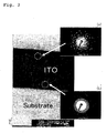
- FIG. 2(a) is an electron diffraction image showing that the thick part of the ITO film, which is away from a substrate, is crystal-like, and FIG.
- FIG. 2(b) is an electron diffraction image showing that the thin part of the ITO film, which is close to the substrate, is amorphous.
- FIG. 2(a) though the ITO film was amorphous and a crystal diffraction pattern could not be confirmed before measurement, a part of ITO was crystallized by an electron beam during the measurement and a crystal diffraction pattern was confirmed. The results revealed that the thick part of the ITO film had a crystal-like structure.
- FIG. 2(b) an electron beam diffraction image did not change and a crystal diffraction pattern could not be confirmed before and after the electron beam analysis.
- ITO in the case of ITO, since a substrate with a patterned ITO is heated at a postbake process or an SiNx process, the ITO changes to a polycrystalline ITO (p-ITO) even if ITO is an amorphous ITO (a-ITO).
- ITZO ITZO is not crystallized by heating at a postbake process or an SiNx process. That is to say, the multilayer structure of the invention may be crystalline or amorphous.
- the molybdenum metal thin film may be composed of a molybdenum monolayer or multiple layers such as a molybdenum/aluminum/molybdenum multilayer.
- the multilayer structure of the invention can be produced by forming the transparent conductive thin film and molybdenum metal thin film by sputtering.
- the discharge gas pressure is normally 0.1 to 1 Pa
- the substrate temperature is normally room temperature to 400°C.
- the film formation gas be argon, or a mixture of argon and oxygen.
- Specific examples of the method for producing the multilayer structure of the invention include the following method (amorphous ITO (a-ITO) method).
- an electrode for an electrical circuit as well as an electrical circuit, can be produced. They can be used in an electronic device.
- the multilayer structure of the invention can be used as an electrical circuit of electronic devices such as liquid crystal displays, organic electroluminescence devices and plasma display panels.
- a 10 nm-thick ITO thin film was formed on a 10 cm-square glass substrate, and then a 150 nm-thick Mo thin film was formed thereon.
- the thicknesses of the above films were measured with an optical thin film measurement system (Film Tek 4000 supplied by SCI Co.) and thickness meter (Dektak 8 supplied by ULVAC, Inc.)
- the ITO thin film formation conditions were as follows:
- the resulting multilayer body was notched in squares, and the tape peel test was conducted to confirm the peeling state.
- the following scratch test was conducted.
- As the scratch tester a micro-scratch-tester supplied by CSME was used.
- the conditions for measuring the peel strength were as follows:
- Multilayer bodies were produced and evaluated under the same conditions as those in Example 1, except that the thicknesses of the ITO film was changed to those as in Table 1.
- a multilayer body was produced and evaluated under the same conditions as those in Example 1, except that the thicknesses of the ITO film was changed to those as shown in Table 1.
- Table 1 Trasnparent electrode Thickness (nm) Tape peel test Scratch peel test (N) Example 1 ITO 10 No peeling occurred 8.72 Example 2 ITO 20 No peeling occurred 8.59 Comparative example 1 ITO 30 No peeling occurred 7.37 Example 3 ITZO 25 No peeling occurred 9.83 Comparative example 2 ITO 40 Partial peeling occurred 5.09 Comparative example 3 ITO 100 No peeling occurred 1.11 Table 1 revealed that no peeling could be seen when the ITO film had a thickness of 25 nm or less, and the adhesiveness therebetween was strong. Table 1 revealed that the adhesiveness between the ITO film and the Molybdenum film worsened rapidly when the ITO film had a thickness of more than 25 nm.
- Multilayer bodies were produced under the same conditions as those in Example 1, except that the thicknesses of the ITO film was changed to 30 nm and 100 nm.
- the multilayer bodies obtained were patterned by the following method and taper angles of the ITO films were measured.
- the taper angle of the ITO thin film patterned by the above-mentioned method was measured with an SEM (scanning electron microscope).
- the taper angle of 30 nm thick ITO film was 80°.
- the taper angle of 100 nm thick ITO film was 150°.
- the multilayer structure of the invention can be used as an electrode for an electrical circuit of an electronic device, and can be used for producing an electric circuit of an electronic device using the electrode.
Landscapes
- Chemical & Material Sciences (AREA)
- Physics & Mathematics (AREA)
- Engineering & Computer Science (AREA)
- Nonlinear Science (AREA)
- Chemical Kinetics & Catalysis (AREA)
- Materials Engineering (AREA)
- Mechanical Engineering (AREA)
- Metallurgy (AREA)
- Organic Chemistry (AREA)
- Manufacturing & Machinery (AREA)
- Crystallography & Structural Chemistry (AREA)
- Mathematical Physics (AREA)
- General Physics & Mathematics (AREA)
- Optics & Photonics (AREA)
- Non-Insulated Conductors (AREA)
- Electroluminescent Light Sources (AREA)
- Internal Circuitry In Semiconductor Integrated Circuit Devices (AREA)
- Liquid Crystal (AREA)
- Devices For Indicating Variable Information By Combining Individual Elements (AREA)
- Parts Printed On Printed Circuit Boards (AREA)
Claims (6)
- Mehrschichtstruktur umfassend einen transparenten leitfähigen Dünnfilm und einen Molybdän-Metall-Dünnfilm, worin
der transparente leitfähige Dünnfilm eine Dicke von 25 nm bis 1 nm und einen Kegelwinkel von weniger als 90° aufweist. - Mehrschichtstruktur nach Anspruch 1, worin der transparente leitfähige Dünnfilm ein Dünnfilm enthaltend Indiumoxid und Zinnoxid ist.
- Mehrschichtstruktur nach Anspruch 1, worin der transparente leitfähige Dünnfilm ein Dünnfilm enthaltend Indiumoxid, Zinnoxid und Zinkoxid ist.
- Mehrschichtstruktur nach Anspruch 1, worin der transparente leitfähige Dünnfilm ein Dünnfilm enthaltend Indiumoxid und ein Oxid eines Seltenerdelements ist.
- Elektrode für eine elektrische Schaltung, umfassend die Mehrschichtstruktur nach der Ansprüche 1 bis 4.
- Elektronische Vorrichtung, umfassend, wenigstens als ein Teil davon, die Mehrschichtstruktur nach einem der Ansprüche 1 bis 4 oder eine elektrische Schaltung, umfassend die Elektrode für eine elektrische Schaltung nach Anspruch 5.
Applications Claiming Priority (2)
| Application Number | Priority Date | Filing Date | Title |
|---|---|---|---|
| JP2006016974 | 2006-01-25 | ||
| PCT/JP2007/050497 WO2007086280A1 (ja) | 2006-01-25 | 2007-01-16 | 積層構造及びそれを用いた電気回路用電極 |
Publications (3)
| Publication Number | Publication Date |
|---|---|
| EP1978400A1 EP1978400A1 (de) | 2008-10-08 |
| EP1978400A4 EP1978400A4 (de) | 2010-03-03 |
| EP1978400B1 true EP1978400B1 (de) | 2012-08-08 |
Family
ID=38309075
Family Applications (1)
| Application Number | Title | Priority Date | Filing Date |
|---|---|---|---|
| EP07706824A Not-in-force EP1978400B1 (de) | 2006-01-25 | 2007-01-16 | Beschichtete struktur und elektrode für eine elektrische schaltung damit |
Country Status (7)
| Country | Link |
|---|---|
| US (1) | US8957313B2 (de) |
| EP (1) | EP1978400B1 (de) |
| JP (1) | JP5165388B2 (de) |
| KR (1) | KR101345022B1 (de) |
| CN (1) | CN101375204A (de) |
| TW (1) | TWI427378B (de) |
| WO (1) | WO2007086280A1 (de) |
Families Citing this family (3)
| Publication number | Priority date | Publication date | Assignee | Title |
|---|---|---|---|---|
| WO2007086280A1 (ja) | 2006-01-25 | 2007-08-02 | Idemitsu Kosan Co., Ltd. | 積層構造及びそれを用いた電気回路用電極 |
| JP2013122903A (ja) * | 2011-11-10 | 2013-06-20 | Nitto Denko Corp | 有機elデバイス、および、有機elデバイスの製造方法 |
| KR20140055097A (ko) | 2012-10-30 | 2014-05-09 | 삼성디스플레이 주식회사 | 터치 스크린 패널의 제조방법 |
Family Cites Families (21)
| Publication number | Priority date | Publication date | Assignee | Title |
|---|---|---|---|---|
| US5366588A (en) | 1992-03-13 | 1994-11-22 | U.S. Philips Corporation | Method of manufacturing an electrically conductive pattern of tin-doped indium oxide (ITO) on a substrate |
| JPH06130405A (ja) * | 1992-10-21 | 1994-05-13 | Fujitsu Ltd | 液晶表示装置の製造方法 |
| JPH06177082A (ja) * | 1992-12-02 | 1994-06-24 | Hitachi Ltd | Ito膜のエッチング方法 |
| JPH0764112A (ja) | 1993-08-30 | 1995-03-10 | Sanyo Electric Co Ltd | 液晶表示装置とその製造方法 |
| WO1997046054A1 (en) * | 1996-05-29 | 1997-12-04 | Idemitsu Kosan Co., Ltd. | Organic el device |
| KR100238795B1 (ko) | 1997-03-03 | 2000-01-15 | 구본준 | 액정 표시 장치의 구조 및 그 액정 표시 장치의 제조 방법 |
| JPH1117188A (ja) * | 1997-06-23 | 1999-01-22 | Sharp Corp | アクティブマトリクス基板 |
| KR100320661B1 (ko) * | 1998-04-17 | 2002-01-17 | 니시무로 타이죠 | 액정표시장치, 매트릭스 어레이기판 및 그 제조방법 |
| JP3422272B2 (ja) * | 1998-12-17 | 2003-06-30 | 日本板硝子株式会社 | Ito透明導電膜付き基板とその製造方法 |
| JP2000238178A (ja) * | 1999-02-24 | 2000-09-05 | Teijin Ltd | 透明導電積層体 |
| JP3420135B2 (ja) | 1999-10-26 | 2003-06-23 | 日本電気株式会社 | アクティブマトリクス基板の製造方法 |
| US6838696B2 (en) * | 2000-03-15 | 2005-01-04 | Advanced Display Inc. | Liquid crystal display |
| JP4249886B2 (ja) * | 2000-07-25 | 2009-04-08 | シャープ株式会社 | 薄膜半導体装置の製造方法 |
| JP4212025B2 (ja) * | 2002-07-04 | 2009-01-21 | Hoya株式会社 | 反射型マスクブランクス及び反射型マスク並びに反射型マスクの製造方法 |
| KR101002492B1 (ko) | 2002-08-02 | 2010-12-17 | 이데미쓰 고산 가부시키가이샤 | 스퍼터링 타겟, 소결체, 이들을 사용하여 제조한 도전막,유기 el 소자, 및 이것에 사용하는 기판 |
| JP4448648B2 (ja) | 2002-08-02 | 2010-04-14 | 出光興産株式会社 | スパッタリングターゲット及び焼結体それらを利用して製造した導電膜。 |
| KR100980015B1 (ko) | 2003-08-19 | 2010-09-03 | 삼성전자주식회사 | 박막 트랜지스터 표시판 및 그 제조 방법 |
| TW200533787A (en) | 2004-02-25 | 2005-10-16 | Mitsubishi Gas Chemical Co | Etching composition for laminated film including reflective electrode and method for forming laminated wiring structure |
| JP2005277402A (ja) | 2004-02-25 | 2005-10-06 | Mitsubishi Gas Chem Co Inc | 反射電極膜を含む積層膜のエッチング組成物および積層配線構造の形成方法 |
| JP2007191761A (ja) | 2006-01-19 | 2007-08-02 | Idemitsu Kosan Co Ltd | 積層構造、それを用いた電気回路用電極及びその製造方法 |
| WO2007086280A1 (ja) | 2006-01-25 | 2007-08-02 | Idemitsu Kosan Co., Ltd. | 積層構造及びそれを用いた電気回路用電極 |
-
2007
- 2007-01-16 WO PCT/JP2007/050497 patent/WO2007086280A1/ja not_active Ceased
- 2007-01-16 CN CNA2007800035210A patent/CN101375204A/zh active Pending
- 2007-01-16 US US12/162,028 patent/US8957313B2/en not_active Expired - Fee Related
- 2007-01-16 JP JP2007555892A patent/JP5165388B2/ja not_active Expired - Fee Related
- 2007-01-16 EP EP07706824A patent/EP1978400B1/de not_active Not-in-force
- 2007-01-22 TW TW096102359A patent/TWI427378B/zh not_active IP Right Cessation
-
2008
- 2008-07-24 KR KR1020087018199A patent/KR101345022B1/ko not_active Expired - Fee Related
Also Published As
| Publication number | Publication date |
|---|---|
| US8957313B2 (en) | 2015-02-17 |
| EP1978400A1 (de) | 2008-10-08 |
| JPWO2007086280A1 (ja) | 2009-06-18 |
| US20090008124A1 (en) | 2009-01-08 |
| KR101345022B1 (ko) | 2013-12-26 |
| TWI427378B (zh) | 2014-02-21 |
| WO2007086280A1 (ja) | 2007-08-02 |
| KR20080087134A (ko) | 2008-09-30 |
| EP1978400A4 (de) | 2010-03-03 |
| CN101375204A (zh) | 2009-02-25 |
| TW200732799A (en) | 2007-09-01 |
| JP5165388B2 (ja) | 2013-03-21 |
Similar Documents
| Publication | Publication Date | Title |
|---|---|---|
| TWI569191B (zh) | A substrate having a transparent electrode, a method for manufacturing the same, and a touch panel | |
| CN103443748B (zh) | 带有透明电极的基板及其制造方法以及触摸面板 | |
| KR101085271B1 (ko) | 표시 디바이스용 Al 합금막, 표시 디바이스 및 스퍼터링 타깃 | |
| CN111128877B (zh) | 刻蚀阻挡型阵列基板的制备方法 | |
| TWI504765B (zh) | Cu alloy film, and a display device or an electronic device provided therewith | |
| US20070241364A1 (en) | Substrate with transparent conductive film and patterning method therefor | |
| JP2009265629A (ja) | 表示用基板及びその製造方法並びに表示装置 | |
| WO2007063991A1 (ja) | 薄膜トランジスタ基板および表示デバイス | |
| KR101926199B1 (ko) | 은 박막의 식각액 조성물 및 이를 이용한 금속 패턴의 형성방법 | |
| EP1978400B1 (de) | Beschichtete struktur und elektrode für eine elektrische schaltung damit | |
| US8017868B2 (en) | Multilayer structure, electrode for electrical circuit using the same, and method for producing the same | |
| CN102543892B (zh) | 一种薄膜晶体管基板及其制造方法和液晶显示装置 | |
| KR102599939B1 (ko) | 은 박막 식각액 조성물 및 이를 이용한 식각 방법 및 금속 패턴의 형성 방법 | |
| CN110408887B (zh) | 晶圆级硅基铝表面的ito透明导电层的制备方法 | |
| KR101182013B1 (ko) | 박막 트랜지스터 기판 및 박막 트랜지스터 기판을 구비한 표시 디바이스 | |
| CN100524780C (zh) | 非保形绝缘薄膜形成方法和应用 | |
| KR100408768B1 (ko) | 이온빔 보조전자빔을 갖는 진공증착기로 완성한 수지계평판표시소자 및 그 제조방법 | |
| US7999907B2 (en) | Method for producing color filter, color filter, liquid crystal display device and producing apparatus | |
| JP4920266B2 (ja) | 積層構造体を有する基板の製造方法 | |
| TW200538800A (en) | A wiring substrate and method using the same | |
| KR101188967B1 (ko) | 표시용 기판 및 그 제조방법과 표시장치 | |
| TW202244546A (zh) | 附無機膜之基板及其製造方法 | |
| JP2001307567A (ja) | 透明導電膜付き基板及びその製造方法 | |
| JP2005026013A (ja) | 透明電極膜付基板および透明電極膜付基板を有するエレクトロルミネッセンス素子 |
Legal Events
| Date | Code | Title | Description |
|---|---|---|---|
| PUAI | Public reference made under article 153(3) epc to a published international application that has entered the european phase |
Free format text: ORIGINAL CODE: 0009012 |
|
| 17P | Request for examination filed |
Effective date: 20080704 |
|
| AK | Designated contracting states |
Kind code of ref document: A1 Designated state(s): DE FR GB |
|
| DAX | Request for extension of the european patent (deleted) | ||
| RBV | Designated contracting states (corrected) |
Designated state(s): DE FR GB |
|
| A4 | Supplementary search report drawn up and despatched |
Effective date: 20100203 |
|
| 17Q | First examination report despatched |
Effective date: 20100422 |
|
| GRAP | Despatch of communication of intention to grant a patent |
Free format text: ORIGINAL CODE: EPIDOSNIGR1 |
|
| GRAS | Grant fee paid |
Free format text: ORIGINAL CODE: EPIDOSNIGR3 |
|
| GRAA | (expected) grant |
Free format text: ORIGINAL CODE: 0009210 |
|
| AK | Designated contracting states |
Kind code of ref document: B1 Designated state(s): DE FR GB |
|
| REG | Reference to a national code |
Ref country code: GB Ref legal event code: FG4D |
|
| REG | Reference to a national code |
Ref country code: DE Ref legal event code: R096 Ref document number: 602007024544 Country of ref document: DE Effective date: 20121004 |
|
| PLBE | No opposition filed within time limit |
Free format text: ORIGINAL CODE: 0009261 |
|
| STAA | Information on the status of an ep patent application or granted ep patent |
Free format text: STATUS: NO OPPOSITION FILED WITHIN TIME LIMIT |
|
| 26N | No opposition filed |
Effective date: 20130510 |
|
| REG | Reference to a national code |
Ref country code: DE Ref legal event code: R097 Ref document number: 602007024544 Country of ref document: DE Effective date: 20130510 |
|
| REG | Reference to a national code |
Ref country code: FR Ref legal event code: PLFP Year of fee payment: 9 |
|
| PGFP | Annual fee paid to national office [announced via postgrant information from national office to epo] |
Ref country code: DE Payment date: 20150113 Year of fee payment: 9 |
|
| PGFP | Annual fee paid to national office [announced via postgrant information from national office to epo] |
Ref country code: GB Payment date: 20150114 Year of fee payment: 9 Ref country code: FR Payment date: 20150108 Year of fee payment: 9 |
|
| REG | Reference to a national code |
Ref country code: DE Ref legal event code: R119 Ref document number: 602007024544 Country of ref document: DE |
|
| GBPC | Gb: european patent ceased through non-payment of renewal fee |
Effective date: 20160116 |
|
| REG | Reference to a national code |
Ref country code: FR Ref legal event code: ST Effective date: 20160930 |
|
| PG25 | Lapsed in a contracting state [announced via postgrant information from national office to epo] |
Ref country code: GB Free format text: LAPSE BECAUSE OF NON-PAYMENT OF DUE FEES Effective date: 20160116 Ref country code: DE Free format text: LAPSE BECAUSE OF NON-PAYMENT OF DUE FEES Effective date: 20160802 |
|
| PG25 | Lapsed in a contracting state [announced via postgrant information from national office to epo] |
Ref country code: FR Free format text: LAPSE BECAUSE OF NON-PAYMENT OF DUE FEES Effective date: 20160201 |