EP1976336A2 - Heizvorrichtung - Google Patents
Heizvorrichtung Download PDFInfo
- Publication number
- EP1976336A2 EP1976336A2 EP08251092A EP08251092A EP1976336A2 EP 1976336 A2 EP1976336 A2 EP 1976336A2 EP 08251092 A EP08251092 A EP 08251092A EP 08251092 A EP08251092 A EP 08251092A EP 1976336 A2 EP1976336 A2 EP 1976336A2
- Authority
- EP
- European Patent Office
- Prior art keywords
- ceramic base
- heating
- heating device
- support member
- concave surface
- Prior art date
- Legal status (The legal status is an assumption and is not a legal conclusion. Google has not performed a legal analysis and makes no representation as to the accuracy of the status listed.)
- Granted
Links
Images

Classifications
-
- H—ELECTRICITY
- H05—ELECTRIC TECHNIQUES NOT OTHERWISE PROVIDED FOR
- H05B—ELECTRIC HEATING; ELECTRIC LIGHT SOURCES NOT OTHERWISE PROVIDED FOR; CIRCUIT ARRANGEMENTS FOR ELECTRIC LIGHT SOURCES, IN GENERAL
- H05B3/00—Ohmic-resistance heating
- H05B3/20—Heating elements having extended surface area substantially in a two-dimensional [2D] plane, e.g. plate-heater
- H05B3/22—Heating elements having extended surface area substantially in a two-dimensional [2D] plane, e.g. plate-heater non-flexible
- H05B3/28—Heating elements having extended surface area substantially in a two-dimensional [2D] plane, e.g. plate-heater non-flexible heating conductor embedded in insulating material
- H05B3/283—Heating elements having extended surface area substantially in a two-dimensional [2D] plane, e.g. plate-heater non-flexible heating conductor embedded in insulating material the insulating material being an inorganic material, e.g. ceramic
-
- H—ELECTRICITY
- H10—SEMICONDUCTOR DEVICES; ELECTRIC SOLID-STATE DEVICES NOT OTHERWISE PROVIDED FOR
- H10P—GENERIC PROCESSES OR APPARATUS FOR THE MANUFACTURE OR TREATMENT OF DEVICES COVERED BY CLASS H10
- H10P95/00—Generic processes or apparatus for manufacture or treatments not covered by the other groups of this subclass
- H10P95/90—Thermal treatments, e.g. annealing or sintering
-
- H—ELECTRICITY
- H10—SEMICONDUCTOR DEVICES; ELECTRIC SOLID-STATE DEVICES NOT OTHERWISE PROVIDED FOR
- H10P—GENERIC PROCESSES OR APPARATUS FOR THE MANUFACTURE OR TREATMENT OF DEVICES COVERED BY CLASS H10
- H10P72/00—Handling or holding of wafers, substrates or devices during manufacture or treatment thereof
- H10P72/04—Apparatus for manufacture or treatment
- H10P72/0431—Apparatus for thermal treatment
- H10P72/0432—Apparatus for thermal treatment mainly by conduction
-
- H—ELECTRICITY
- H10—SEMICONDUCTOR DEVICES; ELECTRIC SOLID-STATE DEVICES NOT OTHERWISE PROVIDED FOR
- H10P—GENERIC PROCESSES OR APPARATUS FOR THE MANUFACTURE OR TREATMENT OF DEVICES COVERED BY CLASS H10
- H10P72/00—Handling or holding of wafers, substrates or devices during manufacture or treatment thereof
- H10P72/70—Handling or holding of wafers, substrates or devices during manufacture or treatment thereof for supporting or gripping
- H10P72/76—Handling or holding of wafers, substrates or devices during manufacture or treatment thereof for supporting or gripping using mechanical means, e.g. clamps or pinches
- H10P72/7604—Handling or holding of wafers, substrates or devices during manufacture or treatment thereof for supporting or gripping using mechanical means, e.g. clamps or pinches the wafers being placed on a susceptor, stage or support
- H10P72/7624—Handling or holding of wafers, substrates or devices during manufacture or treatment thereof for supporting or gripping using mechanical means, e.g. clamps or pinches the wafers being placed on a susceptor, stage or support characterised by the mechanical construction of the susceptor, stage or support
-
- H—ELECTRICITY
- H10—SEMICONDUCTOR DEVICES; ELECTRIC SOLID-STATE DEVICES NOT OTHERWISE PROVIDED FOR
- H10P—GENERIC PROCESSES OR APPARATUS FOR THE MANUFACTURE OR TREATMENT OF DEVICES COVERED BY CLASS H10
- H10P72/00—Handling or holding of wafers, substrates or devices during manufacture or treatment thereof
- H10P72/70—Handling or holding of wafers, substrates or devices during manufacture or treatment thereof for supporting or gripping
- H10P72/76—Handling or holding of wafers, substrates or devices during manufacture or treatment thereof for supporting or gripping using mechanical means, e.g. clamps or pinches
- H10P72/7604—Handling or holding of wafers, substrates or devices during manufacture or treatment thereof for supporting or gripping using mechanical means, e.g. clamps or pinches the wafers being placed on a susceptor, stage or support
- H10P72/7626—Handling or holding of wafers, substrates or devices during manufacture or treatment thereof for supporting or gripping using mechanical means, e.g. clamps or pinches the wafers being placed on a susceptor, stage or support characterised by the construction of the shaft
-
- H—ELECTRICITY
- H05—ELECTRIC TECHNIQUES NOT OTHERWISE PROVIDED FOR
- H05B—ELECTRIC HEATING; ELECTRIC LIGHT SOURCES NOT OTHERWISE PROVIDED FOR; CIRCUIT ARRANGEMENTS FOR ELECTRIC LIGHT SOURCES, IN GENERAL
- H05B2203/00—Aspects relating to Ohmic resistive heating covered by group H05B3/00
- H05B2203/014—Heaters using resistive wires or cables not provided for in H05B3/54
Definitions
- the present invention relates to a heating device made of ceramics, and more specifically, relates to a heating device for heating a wafer to be used as a substrate in a manufacturing process of a semiconductor device or heating other plate-like heating objects.
- heating treatment is implemented for forming an oxide film and the like on a wafer.
- the heating device for heating the wafer there is a heating device that includes a disc-like ceramic base having a heating surface opposite to the wafer as a heating object, in which a resistance heating element is embedded in the ceramic base.
- This heating device is suitable not only for a deposition apparatus in the manufacturing process of the semiconductor device but also advantageously for a surface treatment apparatus that performs dry etching for a surface of the heating object, and the like.
- heating device that further includes a support member for supporting the ceramic base, in which the support member is bonded to the ceramic base.
- This support member has a substantially cylindrical shape, in which one end surface is fixedly attached to an opposite surface of the ceramic base with the heating surface, that is, to a back surface thereof by solid-phase bonding or liquid-phase bonding.
- a heating device made of ceramics, of the present invention includes: a plate-like heating base having a heating surface; and a hollow cylindrical support member bonded to a back surface of the heating base so that an axis direction thereof can be substantially perpendicular to the back surface, wherein a concave surface portion that connects the back surface of the heating base and an outer surface of the support member smoothly to each other is formed in a vicinity of a bonded portion between the heating base and the support member, and on a cross section including an axis of the support member, the concave surface portion has a curved line of an arc of a ellipsoid in which a minor axis direction is parallel to the axis direction of the support member, and in the concave surface portion, a ratio B/A of the major axis radius B of the ellipsoid with respect to the minor axis radius A of the ellipsoid is 1.5 or more on the cross section including the cross section including the cross section including the cross section including
- the crack is suppressed from occurring in the vicinity of the bonded portion between the heating base and the support member, thus making it possible to enhance the reliability of the heating device concerned.
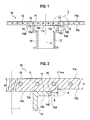
- FIG. 1 is a schematic longitudinal cross-sectional view of an embodiment of the heating device according to the present invention.
- the heating device 10 shown in this drawing includes, as a heating base, a ceramic base 11 made of disc-like ceramics.
- the ceramic base 11 has a planar heating surface 11a on which a heating object (for example, a semiconductor wafer; not shown) is to be mounted.
- a resistance heating element 12 is embedded in an inside of the ceramic base 11. Electric power is supplied from an external power supply (not shown) to the resistance heating element 12, whereby the resistance heating element 12 generates heat. By such heat generation of the resistance heating element 12, the ceramic base 11 is heated.
- the ceramic base 11 is heated, thus making it possible to heat the heating object mounted on the heating surface 11a of the ceramic base 11.
- a shaft 13 as a support member that supports the ceramic base 11 is bonded to a back surface 11b of the ceramic base 11, which is an opposite side surface with the heating surface 11a.
- a plate thickness of the vicinity of a central portion on the back surface 11b is larger than in the vicinity of a peripheral portion thereon, and the shaft 13 is bonded to a surface 11c of the central portion of the back surface 11b.
- the shaft 13 has a substantially cylindrical shape that is hollow, and preferably, is made of the same type of ceramics as that of the ceramic base 11.
- a lead wire and a power feeding bar which are for supplying the electric power to the resistance heating element 12 in the inside of the ceramic base 11, are arranged.
- the ceramic base 11 further includes an electrostatic electrode and a high frequency electrode, lead wires and the like, which are connected to these electrodes embedded in the ceramic base 11, are arranged in the inner space of the shaft 13.
- a flange portion 13a is formed on an end portion of the shaft 13 on a side where the shaft 13 is bonded to the ceramic base 11.
- the shaft 13 is bonded to the ceramic base 11 by solid-phase bonding or liquid-phase bonding.
- a concave surface portion 15 is formed, which smoothly connects the back surface 11b of the ceramic base 11 and an outer circumferential surface 13d of the flange portion 13a of the shaft 13 to each other.
- FIG. 2 An enlarged cross-sectional view of a region II in the vicinity of the concave surface portion 15 of the heating device 10 is shown in FIG. 2 .
- the concave surface portion 15 has a shape that becomes a curved line of an arc of a ellipsoid on a cross section including an axis L of the shaft 13, that is, on a longitudinal cross section shown in FIG. 2 .
- the minor axis direction of this ellipsoid is parallel to the axis L of the shaft 13, and the major axis direction thereof is perpendicular to the axis L of the shaft 13.
- the concave surface portion 15 becomes such a curved surface that becomes the arc of the ellipsoid on the longitudinal cross section. Accordingly, a crack is more effectively suppressed from occurring on the concave surface portion 15. This will be described below in detail.
- FIG. 3 is a longitudinal cross-sectional view of the vicinity of the bonded portion of the conventional heating device including the rounded portion.
- the shaft 13 is bonded to a central surface 21c of a back surface 21b on an opposite side with a heating surface 21a in a ceramic base 21 in which the resistance heating element 12 is embedded.
- a rounded portion 25 is formed, which connects the back surface 21b of the ceramic base 21 and the flange portion 13a of the shaft 13 smoothly to each other with a fixed curvature radius R1.
- the heating device 20 shown in FIG. 3 when the resistance heating body 12 embedded in the ceramic base 21 generates heat, though a portion of the heating surface 21a of the ceramic base 21 is heated uniformly, a temperature of a portion of the bonding interface 24 connected to the shaft 13 becomes lower than temperatures of other portions of the base 21 owing to heat transfer to the shaft 13 through the bonding interface 24.
- the thermal stress is caused in a radius direction of the ceramic base 21 by a temperature gradient in the base 21 concerned.
- a position on which the thermal stress is concentrated most is a position of a maximum stress portion ⁇ 2max located on a middle of the rounded portion 25. Therefore, the crack has sometimes occurred in the vicinity of the maximum stress portion ⁇ 2max on a surface of the rounded portion 25.
- FIG. 4 is a longitudinal cross-sectional view of the vicinity of a bonded portion of a heating device 30, in which the curvature radius of the rounded portion is larger than that of the heating device 20 shown in FIG. 3 .
- the shaft 13 is bonded to a central surface 31c of a back surface 31b on an opposite side with a heating surface 31a in a ceramic base 31 in which the resistance heating element 12 is embedded.
- a rounded portion 35 is formed, which connects the back surface 31b of the ceramic base 31 and the flange portion 13a of the shaft 13 smoothly to each other with a fixed curvature radius R2 larger than the curvature radius R1 of the rounded portion of FIG. 3 .
- the curvature radius R2 of the rounded portion 35 is larger than the curvature radius R1 of the rounded portion 25 of the heating device 20 shown in FIG. 3 . Accordingly, a maximum stress ⁇ 3max of a middle portion of the rounded portion 35 becomes a value smaller than the maximum stress ⁇ 2max of the heating device 20 shown in FIG. 3 .
- the occurrence of the crack is suppressed more than in the heating device 20 shown in FIG. 3 .
- a thickness t2 of the ceramic base 31 is increased more than a thickness t0 of the ceramic base 21 shown in FIG.
- the concave surface portion 15 becomes such a curved surface that becomes the arc of the ellipsoid on the longitudinal cross section, the minor axis direction of the ellipsoid is parallel to the axis direction of the shaft 13, and the major axis direction of the ellipsoid is perpendicular to the axis direction of the shaft 13.
- the heating device 10 of this embodiment includes the concave surface portion 15 as described above, whereby the curvature radius of the portion of the concave surface portion 15, which is in the vicinity of the portion connected to the back surface 11b of the ceramic base 11, is particularly increased.
- the maximum stress ⁇ 1max of the thermal stress in the concave surface portion 15 can be set at a value smaller than the maximum stress ⁇ 3max in the rounded portion 35 of the heating device shown in FIG. 4 . Therefore, the occurrence of the crack is suppressed more effectively.
- the position of the maximum stress ⁇ 1max of the concave surface portion 15 is sufficiently apart from the outer end 14E of the bonding interface 14 between the ceramic base 11 and the shaft 13. Hence, the crack is suppressed from occurring in the outer edge 14E of the boding interface 14 by the maximum stress ⁇ 1max. Also in such a way, the occurrence of the crack is further suppressed in the heating device 10 of this embodiment.
- the thickness t0 of the ceramic base 11 be increased as much as the thickness t2 of the ceramic base 31 of the heating device shown in FIG. 4 .
- the risk of the occurrence of the crack owing to the internal defect caused by increasing the thickness t0 of the ceramic base 11 can be suppressed, and the occurrence of the crack is suppressed also in this point.
- the crack is suppressed by these ways, thus making it possible to enhance the reliability of the heating device.
- a ratio B/A of a maj or axis radius B of the ellipsoid with respect to a minor axis radius A thereof be 1.5 or more.
- the ratio B/A of the major axis radius B with respect to the minor axis radius A is 1.5 or more, whereby the maximum stress ⁇ 1max can be effectively reduced, and the position of the maximum stress ⁇ 1max can be spaced sufficiently apart from the outer end 14E of the bonding interface 14. Hence, the crack can be suppressed significantly.
- An upper limit of the ratio B/A of the major axis radius B of the ellipsoid with respect to the minor axis radius A thereof is not particularly limited from a viewpoint of suppressing the crack.
- the ratio B/A can be set within an appropriate range in consideration for a process margin of the concave surface portion 15, a heat capacity in the vicinity of the central portion of the ceramic base 21, and the like.
- the upper limit of the ratio B/A can be preferably set at 10 or less, more preferably 5 or less.
- a surface roughness of the concave surface portion 15 be 0.8 ⁇ m or less in a centerline average roughness Ra.
- the minor axis radius A of the arc of the concave surface portion 15 is not particularly limited, and moreover, it is preferable that the minor axis radius A be approximately 1 to 10 mm though depending on the thickness t0 of the ceramic base 11. It is more preferable that the minor axis radius A be 2 to 9 mm.
- the formation of the concave surface portion 15 is performed by removing, by a grinding process, a portion of the ceramic base 11 having the thickness t0, which is other than the vicinity of the central portion thereof, and setting the peripheral side of the ceramic base 11 concerned at the thickness t1. Accordingly, in consideration for a margin for the grinding process, and the like, an appropriate value can be selected for the minor axis radius A.
- the thickness t0 of the vicinity of the central portion of the ceramic base 11 is not particularly limited; however, is preferably within a range of 2 to 50 mm, more preferably within a range of 5 to 30 mm.
- the concave surface portion 15 has the shape of the arc of the substantial ellipsoid on the longitudinal cross section. Accordingly, the thickness of the concave surface portion 15 does not have to be limited in order to absorb the stress concentrated thereon, and can be selected appropriately in accordance with other conditions.
- the shape of the arc of the ellipsoid in the heating device of the present invention is not limited to a shape of an arc of an ellipsoid in a strict meaning.
- the material of the ceramic base 11 there are preferably: nitride ceramics such as those of aluminum nitride, silicon nitride, boron nitride, mullite, and sialon; silicon carbide; alumina; an alumina-silicon carbide composite material; and the like.
- the material of the ceramic base 11 may be publicly known ceramic materials without being limited to the above.
- aluminum nitride and alumina are particularly preferable.
- the material of the shaft 13 be the same as the material of the ceramic base.
- the heating device of the present invention is manufactured through the respective steps, which are: a fabrication step of the ceramic base 11; a fabrication step of the shaft 13; and a bonding step of the ceramic base 11 and the shaft 13. These respective steps can be performed by the law of the art.
- a plurality of the heating devices were manufactured, in which the position and shape of each concave surface portion in the vicinity of the bonded portion between the ceramic base and the shaft were variously changed.
- Each of the heating devices was manufactured in such a manner that the ceramic base and the shaft were individually fabricated from AlN powder as a raw material by press molding and firing, and were thereafter bonded to each other by the solid-phase bonding method.
- the plurality of heating devices were prepared, in which an outer diameter of each ceramic base was fixed at 348 mm, the thickness (t1 in FIG. 2 , FIG. 3 and FIG. 4 ) of the peripheral portion thereof was fixed at 20 mm, and the shape of the concave surface portion and the thickness (t0 in FIG. 2 and FIG. 3 and t2 in FIG. 4 ) of the central portion of each ceramic base were variously changed.
- an outer diameter of the flange portion was 75 mm
- an inner diameter thereof was 52 mm
- a thickness (length of an outer circumferential portion of the flange in the axis direction) thereof was 5 mm.
- a grit number of a grindstone was set at #200, the number of revolutions of the grindstone was set at 6000 (rpm), and a feeding speed of the grindstone was set at 0.3 mm/min. After the process, the surface roughness Ra of the concave surface portion was 0.9 ⁇ m.
- Each of these heating devices was placed in a chamber that was set to an atmosphere containing corrosive gas with a pressure of 400 Torr. Subsequently, the heating device was heated up to 700°C to be then subjected a continuous heating operation for 10 hours, was then cooled down to 200°C once, and was heated up to 700°C one more time. In such a way, a thermal test was conducted, and the thermal test was performed for predetermined periods. Thereafter, it was investigated whether or not the crack had occurred.
- the concave surface portion in the vicinity of the bonded portion between the ceramic base and the shaft was formed into a shape of an arc of a perfect circle having a fixed curvature radius (2 mm) on the longitudinal cross section, and the crack occurred after one day elapsed.
- the concave surface portion in the vicinity of the bonded portion between the ceramic base and the shaft was formed into a shape of an arc of a perfect circle having a fixed curvature radius (8 mm) on the longitudinal cross section, and this curvature radius was larger than that of Comparative example 1, and the crack occurred after a half year elapsed.
- Comparative example 2 the thickness of the vicinity of the central portion of the ceramic base became larger than that of Comparative example 1, and accordingly, the risk of the occurrence of the crack owing to the internal defect was increased.
- Comparative example 3 the concave surface portion in the vicinity of the bonded portion between the ceramic base and the shaft was formed into a shape of an arc of the ellipsoid on the longitudinal cross section, and the ratio of the major axis radius B of the ellipsoid with respect to the minor axis radius A thereof was 1.2, and the crack occurred after a half year elapsed.
- Examples 1 to 4 are examples in each of which the concave surface portion has the shape of the arc of the ellipsoid on the longitudinal cross section.
- the ratio of the major axis radius B of the ellipsoid with respect to the minor axis radius A thereof was 1.5 or more, no abnormality was observed even after one and half years elapsed, and particularly excellent reliability was exhibited.
- Comparative example 1 having the curvature radius (2 mm) equal to the minor axis radius (2 mm) of Example 3 concerned, it was found out that it is possible to further enhance the reliability by forming the concave surface portion into the ellipsoidal shape in cross section even if the thickness of the central portion was the same.
- Example 3 by comparison of Example 3 with Comparative example 2 having the curvature radius (8 mm) equal to the major axis radius (8 mm) of Example 4 concerned, it was found out that, by forming the concave surface portion into the ellipsoidal shape in cross section, it is possible to further enhance the reliability without increasing the thickness of the central portion of the ceramic base.
- a relationship between the surface roughness and bonding strength of the concave surface portion of the ceramic base was investigated.
- a heating surface used for this evaluation is the one having the same material and size as those of the heating device used in Example 2.
- the heating device for the evaluation the one was used, in which the minor axis radius was 2 mm, the major axis radius was 3.0 mm, the thickness t0 of the vicinity of the central portion of the ceramic base was 21 mm, and the thickness t1 of the vicinity of the peripheral portion thereof was 20 mm.
- Results of performing a finishing grinding process for the concave surface portion while variously changing a size of abrasion grains of the grindstone, a rotation speed of the grindstone and a feeding speed of the grindstone are shown in Table 2 together with the strength of the bonding interface and the surface roughness of the concave surface in the vicinity of the bonding interface. Note that the strength of the bonding interface was obtained by performing a cantilever bending test for a test piece cut out of the heating device for this evaluation.
- the heating device of the present invention is not limited to the descriptions of the embodiments and the drawings, and a large number of modifications are possible within the scope without departing from the gist of the present invention.
- the outer end 14E of the bonding interface 14 between the ceramic base 11 and the shaft 13 is located on the arc between a major axis end portion and minor axis end portion of the concave surface portion 15 that forms the shape of the arc of the ellipsoid on the longitudinal cross section; however, the outer end 14E may be located at a position that coincides with the major axis end portion of the arc of the concave surface portion 15.
Landscapes
- Chemical & Material Sciences (AREA)
- Engineering & Computer Science (AREA)
- Ceramic Engineering (AREA)
- Inorganic Chemistry (AREA)
- Resistance Heating (AREA)
- Drying Of Semiconductors (AREA)
Applications Claiming Priority (1)
| Application Number | Priority Date | Filing Date | Title |
|---|---|---|---|
| JP2007085609 | 2007-03-28 |
Publications (3)
| Publication Number | Publication Date |
|---|---|
| EP1976336A2 true EP1976336A2 (de) | 2008-10-01 |
| EP1976336A3 EP1976336A3 (de) | 2009-05-13 |
| EP1976336B1 EP1976336B1 (de) | 2012-05-23 |
Family
ID=39639041
Family Applications (1)
| Application Number | Title | Priority Date | Filing Date |
|---|---|---|---|
| EP08251092A Ceased EP1976336B1 (de) | 2007-03-28 | 2008-03-27 | Heizvorrichtung |
Country Status (6)
| Country | Link |
|---|---|
| US (1) | US8294069B2 (de) |
| EP (1) | EP1976336B1 (de) |
| JP (1) | JP5107111B2 (de) |
| KR (1) | KR101345482B1 (de) |
| CN (1) | CN101277554B (de) |
| TW (1) | TWI426813B (de) |
Families Citing this family (19)
| Publication number | Priority date | Publication date | Assignee | Title |
|---|---|---|---|---|
| JP5597072B2 (ja) * | 2010-09-07 | 2014-10-01 | 株式会社日本セラテック | シャフトおよび支持装置 |
| US10276410B2 (en) | 2011-11-25 | 2019-04-30 | Nhk Spring Co., Ltd. | Substrate support device |
| US9153463B2 (en) * | 2011-11-25 | 2015-10-06 | Nhk Spring Co., Ltd. | Substrate support device |
| JP5807032B2 (ja) * | 2012-03-21 | 2015-11-10 | 日本碍子株式会社 | 加熱装置及び半導体製造装置 |
| JP6441921B2 (ja) * | 2014-06-27 | 2018-12-19 | 日本碍子株式会社 | 接合構造体 |
| US11096250B2 (en) * | 2014-10-31 | 2021-08-17 | Ngk Spark Plug Co., Ltd. | Ceramic heater and manufacturing method for same |
| US10177024B2 (en) | 2015-05-12 | 2019-01-08 | Lam Research Corporation | High temperature substrate pedestal module and components thereof |
| US9738975B2 (en) | 2015-05-12 | 2017-08-22 | Lam Research Corporation | Substrate pedestal module including backside gas delivery tube and method of making |
| WO2018030433A1 (ja) * | 2016-08-10 | 2018-02-15 | 日本碍子株式会社 | セラミックヒータ |
| US11289355B2 (en) | 2017-06-02 | 2022-03-29 | Lam Research Corporation | Electrostatic chuck for use in semiconductor processing |
| US11469084B2 (en) | 2017-09-05 | 2022-10-11 | Lam Research Corporation | High temperature RF connection with integral thermal choke |
| CN111316418B (zh) * | 2017-11-02 | 2024-01-30 | 日本碍子株式会社 | 半导体制造装置用构件、其制法及成型模具 |
| CN111670491A (zh) | 2018-01-31 | 2020-09-15 | 朗姆研究公司 | 静电卡盘(esc)基座电压隔离 |
| US11086233B2 (en) | 2018-03-20 | 2021-08-10 | Lam Research Corporation | Protective coating for electrostatic chucks |
| US11183368B2 (en) | 2018-08-02 | 2021-11-23 | Lam Research Corporation | RF tuning systems including tuning circuits having impedances for setting and adjusting parameters of electrodes in electrostatic chucks |
| KR20220169652A (ko) | 2021-06-21 | 2022-12-28 | 주식회사 케이에스엠컴포넌트 | 세라믹 히터용 전기 단자 구조 |
| JP7705298B2 (ja) * | 2021-07-29 | 2025-07-09 | 日本特殊陶業株式会社 | セラミックスヒータ |
| KR102518254B1 (ko) | 2021-09-14 | 2023-04-05 | 주식회사 케이에스엠컴포넌트 | 반도체 제조 장치용 가열 장치 |
| JP7783018B2 (ja) * | 2021-11-15 | 2025-12-09 | 日本特殊陶業株式会社 | 電極埋設部材 |
Citations (2)
| Publication number | Priority date | Publication date | Assignee | Title |
|---|---|---|---|---|
| JP2004247745A (ja) | 2001-02-09 | 2004-09-02 | Ngk Insulators Ltd | サセプターの支持構造 |
| JP2007085609A (ja) | 2005-09-21 | 2007-04-05 | Sanden Corp | 冷却システム |
Family Cites Families (13)
| Publication number | Priority date | Publication date | Assignee | Title |
|---|---|---|---|---|
| DE69432383D1 (de) * | 1993-05-27 | 2003-05-08 | Applied Materials Inc | Verbesserungen betreffend Substrathalter geeignet für den Gebrauch in Vorrichtungen für die chemische Abscheidung aus der Dampfphase |
| US6423949B1 (en) * | 1999-05-19 | 2002-07-23 | Applied Materials, Inc. | Multi-zone resistive heater |
| WO2001084885A1 (en) * | 2000-05-02 | 2001-11-08 | Ibiden Co., Ltd. | Ceramic heater |
| JP2002121083A (ja) | 2000-10-10 | 2002-04-23 | Kyocera Corp | セラミック部材と金属部材の接合体及びこれを用いたウエハ支持部材 |
| US6997993B2 (en) * | 2001-02-09 | 2006-02-14 | Ngk Insulators, Ltd. | Susceptor supporting construction |
| JP3554555B2 (ja) | 2001-02-09 | 2004-08-18 | 日本碍子株式会社 | サセプターの支持構造 |
| JP3982674B2 (ja) * | 2001-11-19 | 2007-09-26 | 日本碍子株式会社 | セラミックヒーター、その製造方法および半導体製造装置用加熱装置 |
| JP3909248B2 (ja) | 2002-01-28 | 2007-04-25 | 京セラ株式会社 | 試料加熱装置 |
| JP3534738B2 (ja) * | 2002-03-28 | 2004-06-07 | 日本碍子株式会社 | セラミックサセプターの取付構造、セラミックサセプターの支持構造およびセラミックサセプター用支持部材 |
| JP3520074B2 (ja) * | 2002-03-28 | 2004-04-19 | 日本碍子株式会社 | セラミックサセプターの取付構造、セラミックサセプターの支持構造およびセラミックサセプターの支持部材 |
| JP4026751B2 (ja) | 2002-06-18 | 2007-12-26 | 日本碍子株式会社 | 半導体製造装置およびその製造方法 |
| JP4476701B2 (ja) * | 2004-06-02 | 2010-06-09 | 日本碍子株式会社 | 電極内蔵焼結体の製造方法 |
| JP2007051317A (ja) * | 2005-08-16 | 2007-03-01 | Ngk Insulators Ltd | 加熱装置 |
-
2008
- 2008-03-24 US US12/053,791 patent/US8294069B2/en active Active
- 2008-03-25 TW TW097110523A patent/TWI426813B/zh active
- 2008-03-26 JP JP2008082073A patent/JP5107111B2/ja active Active
- 2008-03-26 KR KR1020080027793A patent/KR101345482B1/ko active Active
- 2008-03-26 CN CN2008100878595A patent/CN101277554B/zh active Active
- 2008-03-27 EP EP08251092A patent/EP1976336B1/de not_active Ceased
Patent Citations (2)
| Publication number | Priority date | Publication date | Assignee | Title |
|---|---|---|---|---|
| JP2004247745A (ja) | 2001-02-09 | 2004-09-02 | Ngk Insulators Ltd | サセプターの支持構造 |
| JP2007085609A (ja) | 2005-09-21 | 2007-04-05 | Sanden Corp | 冷却システム |
Also Published As
| Publication number | Publication date |
|---|---|
| TWI426813B (zh) | 2014-02-11 |
| CN101277554B (zh) | 2012-03-28 |
| KR101345482B1 (ko) | 2013-12-27 |
| US8294069B2 (en) | 2012-10-23 |
| US20080237221A1 (en) | 2008-10-02 |
| JP5107111B2 (ja) | 2012-12-26 |
| EP1976336A3 (de) | 2009-05-13 |
| TW200847832A (en) | 2008-12-01 |
| KR20080088429A (ko) | 2008-10-02 |
| CN101277554A (zh) | 2008-10-01 |
| JP2008270197A (ja) | 2008-11-06 |
| EP1976336B1 (de) | 2012-05-23 |
Similar Documents
| Publication | Publication Date | Title |
|---|---|---|
| EP1976336B1 (de) | Heizvorrichtung | |
| KR100672802B1 (ko) | 기판 가열 장치 및 그 제조 방법 | |
| KR101142000B1 (ko) | 정전척 | |
| US7417206B2 (en) | Heater, wafer heating apparatus and method for manufacturing heater | |
| KR20010076378A (ko) | 반도체 제조 장치용 웨이퍼 지지체와 그 제조 방법 및반도체 제조 장치 | |
| US7060945B2 (en) | Substrate heater and fabrication method for the same | |
| JP3972944B2 (ja) | セラミックスヒータ及びそれを備えた半導体製造装置 | |
| CN112840741A (zh) | 陶瓷加热器 | |
| JP6618409B2 (ja) | 基板保持装置及びその製造方法 | |
| JP2000114354A (ja) | ウエハ支持加熱用ヒータ | |
| KR100832390B1 (ko) | 가열 장치 및 그 제조 방법 | |
| JP4311922B2 (ja) | セラミックス接合体、ウエハ保持体及び半導体製造装置 | |
| US20160126117A1 (en) | Sample holder | |
| JP5127378B2 (ja) | 窒化アルミニウム焼結体およびそれを用いた基板載置装置 | |
| JP2003224044A (ja) | 試料加熱装置及びその製造方法 | |
| JP2007234425A (ja) | 加熱装置 | |
| JP7705298B2 (ja) | セラミックスヒータ | |
| JP4788575B2 (ja) | 半導体製造装置用保持体 | |
| JP2001181054A (ja) | セラミックス基板 | |
| JP4325083B2 (ja) | 半導体製造装置用セラミックスヒータユニットおよび半導体製造装置 | |
| US20040067354A1 (en) | Tray for vapor phase step | |
| JP2006245609A (ja) | セラミックス接合体、ウエハ保持体及び半導体製造装置 | |
| US20070054424A1 (en) | Semiconductor heating heater holder and semiconductor manufacturing apparatus | |
| JP2001062710A (ja) | ウェハ研磨装置用テーブル |
Legal Events
| Date | Code | Title | Description |
|---|---|---|---|
| PUAI | Public reference made under article 153(3) epc to a published international application that has entered the european phase |
Free format text: ORIGINAL CODE: 0009012 |
|
| AK | Designated contracting states |
Kind code of ref document: A2 Designated state(s): AT BE BG CH CY CZ DE DK EE ES FI FR GB GR HR HU IE IS IT LI LT LU LV MC MT NL NO PL PT RO SE SI SK TR |
|
| AX | Request for extension of the european patent |
Extension state: AL BA MK RS |
|
| PUAL | Search report despatched |
Free format text: ORIGINAL CODE: 0009013 |
|
| AK | Designated contracting states |
Kind code of ref document: A3 Designated state(s): AT BE BG CH CY CZ DE DK EE ES FI FR GB GR HR HU IE IS IT LI LT LU LV MC MT NL NO PL PT RO SE SI SK TR |
|
| AX | Request for extension of the european patent |
Extension state: AL BA MK RS |
|
| RIC1 | Information provided on ipc code assigned before grant |
Ipc: H05B 3/28 20060101AFI20080801BHEP Ipc: H01L 21/687 20060101ALI20090404BHEP |
|
| 17P | Request for examination filed |
Effective date: 20091103 |
|
| AKX | Designation fees paid |
Designated state(s): DE FR GB |
|
| GRAP | Despatch of communication of intention to grant a patent |
Free format text: ORIGINAL CODE: EPIDOSNIGR1 |
|
| GRAS | Grant fee paid |
Free format text: ORIGINAL CODE: EPIDOSNIGR3 |
|
| GRAA | (expected) grant |
Free format text: ORIGINAL CODE: 0009210 |
|
| AK | Designated contracting states |
Kind code of ref document: B1 Designated state(s): DE FR GB |
|
| REG | Reference to a national code |
Ref country code: GB Ref legal event code: FG4D |
|
| REG | Reference to a national code |
Ref country code: DE Ref legal event code: R096 Ref document number: 602008015823 Country of ref document: DE Effective date: 20120726 |
|
| PLBE | No opposition filed within time limit |
Free format text: ORIGINAL CODE: 0009261 |
|
| STAA | Information on the status of an ep patent application or granted ep patent |
Free format text: STATUS: NO OPPOSITION FILED WITHIN TIME LIMIT |
|
| 26N | No opposition filed |
Effective date: 20130226 |
|
| REG | Reference to a national code |
Ref country code: DE Ref legal event code: R097 Ref document number: 602008015823 Country of ref document: DE Effective date: 20130226 |
|
| REG | Reference to a national code |
Ref country code: FR Ref legal event code: PLFP Year of fee payment: 9 |
|
| REG | Reference to a national code |
Ref country code: FR Ref legal event code: PLFP Year of fee payment: 10 |
|
| REG | Reference to a national code |
Ref country code: FR Ref legal event code: PLFP Year of fee payment: 11 |
|
| PGFP | Annual fee paid to national office [announced via postgrant information from national office to epo] |
Ref country code: GB Payment date: 20220203 Year of fee payment: 15 Ref country code: DE Payment date: 20220203 Year of fee payment: 15 |
|
| PGFP | Annual fee paid to national office [announced via postgrant information from national office to epo] |
Ref country code: FR Payment date: 20220209 Year of fee payment: 15 |
|
| REG | Reference to a national code |
Ref country code: DE Ref legal event code: R119 Ref document number: 602008015823 Country of ref document: DE |
|
| GBPC | Gb: european patent ceased through non-payment of renewal fee |
Effective date: 20230327 |
|
| PG25 | Lapsed in a contracting state [announced via postgrant information from national office to epo] |
Ref country code: GB Free format text: LAPSE BECAUSE OF NON-PAYMENT OF DUE FEES Effective date: 20230327 |
|
| PG25 | Lapsed in a contracting state [announced via postgrant information from national office to epo] |
Ref country code: GB Free format text: LAPSE BECAUSE OF NON-PAYMENT OF DUE FEES Effective date: 20230327 Ref country code: FR Free format text: LAPSE BECAUSE OF NON-PAYMENT OF DUE FEES Effective date: 20230331 Ref country code: DE Free format text: LAPSE BECAUSE OF NON-PAYMENT OF DUE FEES Effective date: 20231003 |