EP1969601B1 - Speicher mit einem einknotendaten-, adressen- und steuerbus - Google Patents
Speicher mit einem einknotendaten-, adressen- und steuerbus Download PDFInfo
- Publication number
- EP1969601B1 EP1969601B1 EP06848943.4A EP06848943A EP1969601B1 EP 1969601 B1 EP1969601 B1 EP 1969601B1 EP 06848943 A EP06848943 A EP 06848943A EP 1969601 B1 EP1969601 B1 EP 1969601B1
- Authority
- EP
- European Patent Office
- Prior art keywords
- memory
- memory array
- address
- digital system
- instruction
- Prior art date
- Legal status (The legal status is an assumption and is not a legal conclusion. Google has not performed a legal analysis and makes no representation as to the accuracy of the status listed.)
- Active
Links
Images


Classifications
-
- G—PHYSICS
- G11—INFORMATION STORAGE
- G11C—STATIC STORES
- G11C7/00—Arrangements for writing information into, or reading information out from, a digital store
- G11C7/10—Input/output [I/O] data interface arrangements, e.g. I/O data control circuits, I/O data buffers
-
- G—PHYSICS
- G11—INFORMATION STORAGE
- G11C—STATIC STORES
- G11C5/00—Details of stores covered by group G11C11/00
- G11C5/06—Arrangements for interconnecting storage elements electrically, e.g. by wiring
- G11C5/066—Means for reducing external access-lines for a semiconductor memory clip, e.g. by multiplexing at least address and data signals
-
- G—PHYSICS
- G11—INFORMATION STORAGE
- G11C—STATIC STORES
- G11C16/00—Erasable programmable read-only memories
- G11C16/02—Erasable programmable read-only memories electrically programmable
- G11C16/06—Auxiliary circuits, e.g. for writing into memory
- G11C16/10—Programming or data input circuits
- G11C16/102—External programming circuits, e.g. EPROM programmers; In-circuit programming or reprogramming; EPROM emulators
-
- G—PHYSICS
- G11—INFORMATION STORAGE
- G11C—STATIC STORES
- G11C5/00—Details of stores covered by group G11C11/00
- G11C5/06—Arrangements for interconnecting storage elements electrically, e.g. by wiring
-
- G—PHYSICS
- G11—INFORMATION STORAGE
- G11C—STATIC STORES
- G11C8/00—Arrangements for selecting an address in a digital store
- G11C8/04—Arrangements for selecting an address in a digital store using a sequential addressing device, e.g. shift register, counter
-
- G—PHYSICS
- G11—INFORMATION STORAGE
- G11C—STATIC STORES
- G11C2216/00—Indexing scheme relating to G11C16/00 and subgroups, for features not directly covered by these groups
- G11C2216/12—Reading and writing aspects of erasable programmable read-only memories
- G11C2216/30—Reduction of number of input/output pins by using a serial interface to transmit or receive addresses or data, i.e. serial access memory
Definitions
- the present disclosure relates generally to semiconductor memory, e.g ., electrically erasable programmable read only memory (EEPROM), FLASH memory, static random access memory (SRAM), dynamic random access memory (DRAM) and the like, and, more particularly, to a semiconductor memory using a single-node data, address and control bus.
- semiconductor memory e.g ., electrically erasable programmable read only memory (EEPROM), FLASH memory, static random access memory (SRAM), dynamic random access memory (DRAM) and the like, and, more particularly, to a semiconductor memory using a single-node data, address and control bus.
- EEPROM electrically erasable programmable read only memory
- FLASH memory FLASH memory
- SRAM static random access memory
- DRAM dynamic random access memory
- Integrated circuit digital devices e.g., digital processors such as, for example but not limited to, microprocessors, microcontrollers, digital signal processors (DSP), programmable logic array (PLA), application specific integrated circuit (ASIC) and the like, are becoming smaller and with fewer input-output (I/O) signal connections (e.g ., pins) for both cost and space considerations.
- I/O input-output
- an integrated circuit device may be in an integrated circuit package having a plurality of connection pins. At least two of these pins must be used for power and ground, e.g ., V DD and V SS , respectively.
- These integrated circuit devices may benefit from additional memory, e.g ., external memory.
- the memory may be, for example but not limited to, one time programmable (OTP), electrically programmable read only memory (EPROM), electrically erasable and programmable read only memory (EEPROM), FLASH memory, static random access memory (SRAM), dynamic random access memory (DRAM) and the like.
- OTP one time programmable
- EPROM electrically programmable read only memory
- EEPROM electrically erasable and programmable read only memory
- FLASH memory static random access memory (SRAM), dynamic random access memory (DRAM) and the like.
- US 5,270,972 discloses a three-terminal serial digital system wherein a memory is arranged in a low terminal count package and connected to a single node bus (303, fig.3 ) driven by a pull-down driver (385).
- the pull-down driver generates a first or a second acknowledgement signal on the single node bus (303) caused by a control signal (ACK) received from a digital processor (340).
- ACK control signal
- EP 1 496 444 discloses a method of generating an enable signal of a standard memory core.
- US 6,034,898 discloses a dynamic random access memory for increasing a data output driver current shares pull-up transistors and pull-down transistors.
- US 2005/0268022 discloses a cache line memory and method having a serial address port.
- US 5,809,518 discloses a command/data transfer protocol for one-wire-bus architecture.
- a memory array may be coupled to an integrated circuit digital device with a minimum number of connections, e.g ., a single-node data, address and control bus, plus power and ground, e.g ., V DD (or V CC ) and V SS , respectively, may be required for operation of the memory, thus a minimum of a three pin integrated circuit package, e.g ., SOT 23-3, SC70-3, etc ., may be used for packaging the memory.
- a minimum number of connections e.g ., a single-node data, address and control bus, plus power and ground, e.g ., V DD (or V CC ) and V SS , respectively, may be required for operation of the memory, thus a minimum of a three pin integrated circuit package, e.g ., SOT 23-3, SC70-3, etc ., may be used for packaging the memory.
- Memory address selection when implementing a plurality of memories may utilize additional address select pins on a low pin count integrated circuit package, e.g ., SOT 23-5, SOT 23-6, MSOP-8, SOIC-8 and the like, and/or by programming a memory address for each of the plurality of memories via the single-node data, address and control bus.
- a low pin count integrated circuit package e.g ., SOT 23-5, SOT 23-6, MSOP-8, SOIC-8 and the like
- a memory using a single-node data, address and control bus comprises a memory array adapted for coupling.to a single-node data, address and control bus, power, and ground.
- the memory array has an active pull-up and pull-down bus driver for driving the single-node data, address and control bus.
- the memory array may be enclosed in a low terminal count integrated circuit package.
- the memory may also be part of a multiple die integrated circuit package housing both the digital device and memory.
- a digital system comprises a digital processor and a memory array coupling to the digital processor through a single-node data, address and control bus.
- the memory array has an active pull-up and pull-down bus driver for driving the single-node data, address and control bus.
- the digital processor may be a master and the memory array may be a slave on the single-node data, address and control bus.
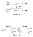
- a digital processor 102 may be coupled to a memory 104 by a single-node data, address and control bus 106.
- the digital processor 102 may be a microprocessor, a microcontroller, a digital signal processor (DSP), a programmable logic array (PLA), an application specific integrated circuit (ASIC) and the like.
- the memory 104 may be non-volatile memory, e.g ., one time programmable (OTP) memory, electrically programmable read only memory (EPROM), electrically erasable and programmable read only memory (EEPROM), FLASH memory and the like.
- the memory 104 may also be volatile memory, e.g ., static random access memory (SRAM), dynamic random access memory (DRAM) and the like.
- the single-node data, address and control bus 106 may be a conductive node, e.g ., printed circuit board conductor, integrated circuit die bond node and the like.
- the digital processor 102 and the memory 104 may have an active pull-up (e.g ., logic '1') and pull-down (e.g ., logic '0') driver coupled to the single-node data, address and control bus 106.
- the digital processor 102 and the memory 104 may be coupled to a common power supply return , e.g ., V SS , ground, etc ., and power, e.g ., V CC , V DD , etc.
- the memory 104 may be packaged in a low pin count integrated circuit package, e.g ., SOT23-3, SOT23-5, SC70-3 and the like. It is contemplated and within the scope of this disclosure that any low pin count integrated circuit package may be used to enclose the memory 104. It is also contemplated and within the scope of the present disclosure that the digital processor 102 and the memory 104 may be packaged in a dual die integrated circuit package wherein the single-node data, address and control bus 106 may be a bond wire (not shown) or other direct die-to-die connection within the integrated circuit package.
- the integrated circuit package may have a ground terminal, V SS ; a power terminal, V DD or V CC ; and a bidirectional serial input-output (I/O) terminal, SCIO.
- V SS ground terminal
- V DD power terminal
- V CC power terminal
- SCIO bidirectional serial input-output
- hardwired memory address selection terminals A0 and A1 may be used when more then three terminals are available on the integrated circuit package. It is contemplated and within the scope of this disclosure that memory block address set-up may be performed via software instructions through the SCIO terminal.
- the single-node data, address and control bus 106 may operate using a bidirectional single-node bus and data transmission protocol.
- a device that sends data onto the bus 106 may be defined as transmitter, and a device receiving data as receiver.
- the bus 106 may be controlled by a master device that may determine a clock period, control bus access and may initiate all operations thereof.
- the memory 104 may be the slave and the digital processor 102 may be the master. Both master and slave may operate as transmitter or receiver, but the master determines which operational mode (master or slave) is activated for each.
- the Start header may consist of, for example but not limited to, an 8-bit binary code (e.g ., 01010101) being output from the transmitting device.
- the signal protocol on the bus 106 may be Manchester-encoded, or any other type of serial transfer signal protocol, e.g ., non-return to zero (NRZ), pulse position modulation (PPM), frequency shift keying (FSK), phase shift keying (PSK), amplitude shift keying (ASK) and the like, that may use an initial Start header byte (or other length word) to synchronize the master and slave clocks together.
- NMR non-return to zero
- PPM pulse position modulation
- FSK frequency shift keying
- PSK phase shift keying
- ASK amplitude shift keying
- Each receiver when addressed, may generate an acknowledge after receiving a certain number of bits, e.g ., each byte (8 bits).
- the receiver may acknowledge by pulling the SCIO terminal high, e.g ., to substantially V DD or V CC , for the first half of a bit, and then low, e.g ., to substantially V SS , for the second (remaining) half of the bit.
- the master may signal an end of data to the slave by generating an acknowledge bit on the last byte that has been clocked out to the slave, e.g ., a "1" (high) may be transmitted, indicating that no more data is to be sent.
- bus reset may take place. Both the master and slave devices may then return to standby modes. Any further commands will be proceeded by a correct Start header to bring the addressed device out of standby.
- FIG. 4 depicted is a diagram of a memory device address byte allocation in a memory, according to a specific example embodiment of the present disclosure.
- the device address may follow the Start header from the master device.
- the device address may consist of a four bit "family code," for example but not limited to, "1010” and the last four bits of the device address byte may be the Chip Select bits ( e.g ., A3, A2, A1 and A0). It is contemplated and within the scope of this disclosure that other bit length family codes may be used.
- FIG. 5 depicted is a table of an instruction set for a memory, according to a specific example embodiment of the present disclosure.
- a command byte may be send by the master to indicate the type of operation to be performed.
- a specific example instruction set is shown in the table of Figure 5 . It is contemplated and within the scope of this disclosure that other and further instructions may be used for an instruction set.
- the Read instruction may be used by the master to access any memory location in a random manner.
- the read data from the memory 104 may begin at a selected address.
- two bytes of the Word Address may be transmitted, wherein the slave may generate an acknowledge (ACK) bit, e.g ., "0," after each byte received. Then the slave may send a first data byte to the master. If more data is to be read, then the master may respond with an acknowledge bit that indicates to the slave to output the next data byte.
- ACK acknowledge
- the memory 104 may have an address pointer that may provide incremental sequential reads upon completion of each read. Thus any number of bytes stored in a sequence of addresses may be serially read from the memory 104 during one multiple read operation.
- FIG. 7 depicts a schematic diagram of signal timing waveforms for a write command sequence of a memory
- Figure 8 depicts a schematic diagram of signal timing waveforms for a write enable command sequence of a memory, according to a specific example embodiment of the present disclosure.
- a write enable (WREN) instruction may be sent by the master, e.g ., digital processor 102, to set a write enable latch (not shown).
- a write instruction (WRITE) may issue (including the header and device address bytes) followed by the most significant byte (MSB) and least significant byte (LSB) of the Word Address.
- MSB most significant byte
- LSB least significant byte
- the write disable (WRDI) instruction may reset the write enable latch (not shown).
- the write enable latch may be reset when the WRDI instruction has successfully executed, the write status register (WRSR) instruction has successfully executed, and/or the WRITE instruction has successfully executed.
- the read status register (RDSR) instruction may provide access to the Status Register (not shown) of the memory 104.
- the Status Register may be read at any time, even during a write operation.
- the Status Register may be formatted as follows: 7 6 5 4 3 2 1 0 X X X X BP1 BP0 WEL WIP
- Bits 4-7 may be reserved for future ID bits.
- a Write-In-Process (WIP) bit may indicate whether the memory 104 is busy with a write operation. For example, when set to a '1,' a write operation may be in progress, when set to a '0,' no write is in progress. The opposite bit sense may also be used. It is contemplated and within the scope of this disclosure that any bit size Status Register may be used, and any number of bits may be reserved as ID bits.
- the Status Register may be a plurality of Status Registers.
- a Write Enable Latch (WEL) bit may indicate the status of a write enable latch (not shown). For example, when set to a '1,' the write enable latch may allow writes to a memory array, when set to a '0,' no writes may be allowed to the memory array. The opposite bit sense may also be used. This bit may be read only.
- Block Protection e.g ., BP0 and BP1 bits may indicate which blocks are currently write protected.
- the BP0 and BP1 bits may be set through the WRSR instruction.
- the BP0 and BP1 bits may be nonvolatile.
- the Write Status Register (WRSR) instruction may allow selection, e.g ., one of four levels, of protection of the memory array by writing to the appropriate bits in the status register.
- the memory array may be divided into segments, e.g ., four segments. Each of the segments may be write protected independently of the other segments. Partitioning of the segments may be controlled as an example, but not limited to, what is indicated in the table below: BP1 BP2 Array Addresses Write Protected 0 0 none 0 1 upper 1/4 of memory array 1 0 upper 1/2 of memory array 1 1 all of memory array
- FIG. 12 depicted is a schematic diagram of signal timing waveforms for an erase all command sequence of a memory, according to a specific example embodiment of the present disclosure.
- the Erase All (ERAL) instruction may be used to reset an entire memory array to all '1's, e.g ., '0xFF', with a single instruction command. Once a write enable latch is set, a ERAL instruction may be issued then the memory array may be reset to '0xFF'.
- the Write All (WRAL) instruction may be used to set an entire memory array to all '0's, e.g ., '0x00', with a single instruction command. Once a write enable latch is set, a WRAL instruction may be issued then the memory array may be set to '0x00'.
Landscapes
- Engineering & Computer Science (AREA)
- Microelectronics & Electronic Packaging (AREA)
- Read Only Memory (AREA)
- Static Random-Access Memory (AREA)
- Dram (AREA)
Claims (15)
- Digitale Anordnung, die aufweist
einen Speicher (104), der einen Einknotendaten-, Adressen- und Steuerbus verwendet und aufweist:ein Speicher-Array (104), geeignet zum Koppeln an
Strom (VDD), und
Masse (VSS);wobei das Speicher-Array (104) in eine IC-Einheit (SOT23-3; SOT23-5) mit geringer Anzahl von Anschlüssen eingebettet ist; undeinen mit dem Speicher-Array (104) gekoppelten Einknotendaten-, Adressen- und Steuerbus (106), wobei das Speicher-Array (104) einen aktiven Pull-Up- und Pull-Down-Bustreiber zum Betreiben des Einknotendaten-, Adressen- und Steuerbus (106) aufweist und wobei das Speicher-Array ein internes Taktsignal des Speichers mittels eines empfangenen Signals synchronisiert; undeinen durch den Einknotendaten-, Adressen- und Steuerbus (106) mit dem Speicher (104) gekoppelten digitalen Prozessor (102), wobei der digitale Prozessor (102) nach dem Empfang eines Datenbyte ein erstes Bestätigungssignal (ACK) auf dem Einknotendaten-, Adressen- und Steuerbus erzeugt; und beim Empfang eines Datenbyte ein zweites Bestätigungssignal (NACK) erzeugt, wenn kein weiteres Datenbyte durch das Speicher-Array (104) gesendet werden soll. - Digitale Anordnung gemäß Anspruch 1, wobei das empfangene Signal einen multi-bit binär kodierten Start-Header aufweist.
- Digitale Anordnung gemäß Anspruch 1 oder 2, wobei das Speicher-Array (104) nach Empfang eines Byte durch den aktiven Pull-Up- und Pull-Down-Bustreiber ein Bestätigungssignal (ACK) erzeugt.
- Digitale Anordnung gemäß einem der vorherigen Ansprüche, die weiterhin zumindest einen Speicheradressauswahlanschluss (A0; A1) aufweist.
- Digitale Anordnung gemäß einem der vorherigen Ansprüche, wobei das Speicher-Array (104) ein serielles Signaltransferprotokoll verwendet, das ausgewählt ist aus der Gruppe bestehend aus Manchester, Pulsdauermodulation (PWM), Non-Return-to-Zero (NRZ), Pulspositionsmodulation (PPM), Frequenzsprungmodulation (FSK), Phasensprungmodulation (PSK), und Amplitudensprungmodulation (ASK).
- Digitale Anordnung gemäß einem der vorherigen Ansprüche, wobei das Speicher-Array (104) eine READ Anweisung aufweist, die beginnend an einer ausgewählten Adresse Daten aus dem Speicher-Array (104) liest, und eine WRITE Anweisung aufweist, die beginnend an einer ausgewählten Adresse Daten in das Speicher-Array (104) schreibt.
- Digitale Anordnung gemäß einem der vorherigen Ansprüche , wobei das Speicher-Array (104) eine WREN Anweisung aufweist, die ein Write-Enable-Auffangregister setzt, um auf diese Weise Schreiboperationen zu ermöglichen, und eine WRDI Anweisung aufweist, die das Write-Enable-Auffangregister zurücksetzt, um auf diese Weise Schreiboperationen zu blockieren.
- Digitale Anordnung gemäß Anspruch 1, wobei das Speicher-Array (104) eine RDSR Anweisung aufweist, die aus einem oder einer Vielzahl von Statusregistern liest, und eine WRSR Anweisung aufweist, die in eines oder die Vielzahl von Statusregistern schreibt.
- Digitale Anordnung gemäß Anspruch 1, wobei das Speicher-Array (104) eine ERAL Anweisung aufweist, die das gesamte Speicher-Array (104) zurücksetzt, und eine WRAL Anweisung aufweist, die das gesamte Speicher-Array (104) setzt.
- Digitale Anordnung gemäß einem der vorherigen Ansprüche, wobei das Speicher-Array (104) ausgewählt ist aus der Gruppe die besteht aus One-Time-Programmable (OTP) Speicher, Electrically Programmable Read Only Memory (EPROM), Electrically Erasable and Programmable Read Only Memory (EEPROM) und FLASH Speicher.
- Digitale Anordnung gemäß einem der vorherigen Ansprüche, wobei die IC-Einheit (SOT23-3) drei Anschlüsse (VSS; VDD; SCIO) aufweist.
- Digitale Anordnung gemäß einem der vorherigen Ansprüche, die weiterhin eine IC-Einheit (SOT23-3; SOT23-5) aufweist, die den digitalen Prozessor (102) und das Speicher-Array (104) einschließt.
- Digitale Anordnung gemäß Anspruch 12, wobei die IC-Einheit (SOT23-3; SOT23-5) eine Einheit mit zwei Chips ist.
- Digitale Anordnung gemäß einem der vorherigen Ansprüche 11 bis 13, wobei der digitale Prozessor (102) ausgewählt ist aus der Gruppe bestehend aus einem Mikroprozessor, einem Mikrocontroller, einem digitalen Signalprozessor (DSP), einem Programmable Logic Array (PLA), und einem Application Specific Integrated Circuit (ASIC).
- Digitale Anordnung gemäß einem der vorherigen Ansprüche 11 bis 14, wobei der digitale Prozessor (102) ein Master ist und das Speicher-Array (104) ein Slave auf dem Einknotendaten-, Adressen- und Steuerbus (106) ist.
Applications Claiming Priority (2)
| Application Number | Priority Date | Filing Date | Title |
|---|---|---|---|
| US11/301,670 US7376020B2 (en) | 2005-12-13 | 2005-12-13 | Memory using a single-node data, address and control bus |
| PCT/US2006/047489 WO2007075336A2 (en) | 2005-12-13 | 2006-12-11 | Memory using a single-node data, address and control bus |
Publications (2)
| Publication Number | Publication Date |
|---|---|
| EP1969601A2 EP1969601A2 (de) | 2008-09-17 |
| EP1969601B1 true EP1969601B1 (de) | 2014-02-12 |
Family
ID=38139132
Family Applications (1)
| Application Number | Title | Priority Date | Filing Date |
|---|---|---|---|
| EP06848943.4A Active EP1969601B1 (de) | 2005-12-13 | 2006-12-11 | Speicher mit einem einknotendaten-, adressen- und steuerbus |
Country Status (7)
| Country | Link |
|---|---|
| US (1) | US7376020B2 (de) |
| EP (1) | EP1969601B1 (de) |
| KR (1) | KR100973185B1 (de) |
| CN (1) | CN101326585B (de) |
| ES (1) | ES2462368T3 (de) |
| TW (1) | TWI397923B (de) |
| WO (1) | WO2007075336A2 (de) |
Families Citing this family (7)
| Publication number | Priority date | Publication date | Assignee | Title |
|---|---|---|---|---|
| US7788430B2 (en) * | 2007-09-14 | 2010-08-31 | Microchip Technology Incorporated | Enhanced single-node protocol for data, address and control operations |
| KR100943137B1 (ko) | 2008-05-13 | 2010-02-18 | 주식회사 하이닉스반도체 | 불휘발성 메모리 장치의 테스트 방법 |
| US8291143B1 (en) * | 2009-02-11 | 2012-10-16 | Brocade Communication Systems, Inc. | Single line communication |
| US9755821B2 (en) | 2015-04-02 | 2017-09-05 | Samsung Electronics Co., Ltd. | Device including single wire interface and data processing system including the same |
| KR102328014B1 (ko) | 2015-08-24 | 2021-11-18 | 삼성전자주식회사 | 싱글 와이어 인터페이스를 포함하는 장치와 이를 포함하는 데이터 처리 시스템 |
| DE102016123400B3 (de) * | 2016-01-19 | 2017-04-06 | Elmos Semiconductor Aktiengesellschaft | Eindrahtlichtsteuerbus mit mehreren Pegeln |
| TWI625915B (zh) * | 2016-11-18 | 2018-06-01 | Industrial Technology Research Institute | 智慧型充電方法 |
Citations (3)
| Publication number | Priority date | Publication date | Assignee | Title |
|---|---|---|---|---|
| EP0206403A2 (de) * | 1985-06-24 | 1986-12-30 | Racal-Datacom Inc. | Paketvermittlungsanordnung hoher Geschwindigkeit |
| US5809518A (en) * | 1989-05-15 | 1998-09-15 | Dallas Semiconductor Corporation | Command/data transfer protocol for one-wire-bus architecture |
| US6034898A (en) * | 1997-06-20 | 2000-03-07 | Hyundai Electronics Industries Co., Ltd. | Dynamic random access memory for increasing a data output driver current |
Family Cites Families (21)
| Publication number | Priority date | Publication date | Assignee | Title |
|---|---|---|---|---|
| US4847867A (en) * | 1986-09-01 | 1989-07-11 | Nec Corporation | Serial bus interface system for data communication using two-wire line as clock bus and data bus |
| US5198999A (en) | 1988-09-12 | 1993-03-30 | Kabushiki Kaisha Toshiba | Serial input/output semiconductor memory including an output data latch circuit |
| US5844842A (en) * | 1989-02-06 | 1998-12-01 | Hitachi, Ltd. | Nonvolatile semiconductor memory device |
| US5270972A (en) * | 1992-04-14 | 1993-12-14 | Xicor, Inc. | Three terminal serial-communicating peripheral device |
| US5508971A (en) * | 1994-10-17 | 1996-04-16 | Sandisk Corporation | Programmable power generation circuit for flash EEPROM memory systems |
| US5847450A (en) | 1996-05-24 | 1998-12-08 | Microchip Technology Incorporated | Microcontroller having an n-bit data bus width with less than n I/O pins |
| US6055204A (en) * | 1997-04-29 | 2000-04-25 | Texas Instruments Incorporated | Circuits, systems, and methods for re-mapping memory column redundancy |
| FR2769744B1 (fr) * | 1997-10-15 | 2001-03-30 | Sgs Thomson Microelectronics | Circuit integre a memoire comprenant un circuit interne de generation d'une haute tension de programmation |
| JP2001273773A (ja) | 2000-03-27 | 2001-10-05 | Sanyo Electric Co Ltd | 半導体メモリ装置 |
| US6505266B1 (en) * | 2000-04-07 | 2003-01-07 | Jing Lu Gu | Method and apparatus for a mix signal module |
| CN1159723C (zh) * | 2000-08-29 | 2004-07-28 | 上海新茂半导体有限公司 | 一种串行存储器 |
| GB0123422D0 (en) * | 2001-09-28 | 2001-11-21 | Memquest Ltd | Improved memory controller |
| US6967591B1 (en) * | 2002-04-15 | 2005-11-22 | Linear Technology Corporation | Multi-bit digital input using a single pin |
| TWI252494B (en) * | 2003-06-11 | 2006-04-01 | Samsung Electronics Co Ltd | Memory system with reduced pin count |
| ITVA20030022A1 (it) | 2003-07-07 | 2005-01-08 | St Microelectronics Srl | Metodo di generazione di un segnale di abilitazione in una memoria multi-protocollo e relativo dispositivo di memoria. |
| US6865113B2 (en) * | 2003-07-23 | 2005-03-08 | Catalyst Semiconductor, Inc. | System and method for programming non-volatile memory |
| TWI258150B (en) * | 2003-12-29 | 2006-07-11 | Inventec Multimedia & Telecom | Portable storage device with prompting function |
| US7315585B2 (en) * | 2004-02-11 | 2008-01-01 | Micrel, Inc. | Clock-less serial data interface using a single pin |
| US20050268022A1 (en) * | 2004-05-26 | 2005-12-01 | Pelley Perry H | Cache line memory and method therefor |
| US7957266B2 (en) * | 2004-05-28 | 2011-06-07 | Alcatel-Lucent Usa Inc. | Efficient and robust routing independent of traffic pattern variability |
| US20060248267A1 (en) * | 2005-04-29 | 2006-11-02 | Programmable Microelectronics Corporation | Flash memory having configurable sector size and flexible protection scheme |
-
2005
- 2005-12-13 US US11/301,670 patent/US7376020B2/en not_active Expired - Lifetime
-
2006
- 2006-12-07 TW TW095145720A patent/TWI397923B/zh active
- 2006-12-11 ES ES06848943.4T patent/ES2462368T3/es active Active
- 2006-12-11 EP EP06848943.4A patent/EP1969601B1/de active Active
- 2006-12-11 WO PCT/US2006/047489 patent/WO2007075336A2/en not_active Ceased
- 2006-12-11 KR KR1020087013238A patent/KR100973185B1/ko active Active
- 2006-12-11 CN CN2006800467277A patent/CN101326585B/zh active Active
Patent Citations (3)
| Publication number | Priority date | Publication date | Assignee | Title |
|---|---|---|---|---|
| EP0206403A2 (de) * | 1985-06-24 | 1986-12-30 | Racal-Datacom Inc. | Paketvermittlungsanordnung hoher Geschwindigkeit |
| US5809518A (en) * | 1989-05-15 | 1998-09-15 | Dallas Semiconductor Corporation | Command/data transfer protocol for one-wire-bus architecture |
| US6034898A (en) * | 1997-06-20 | 2000-03-07 | Hyundai Electronics Industries Co., Ltd. | Dynamic random access memory for increasing a data output driver current |
Also Published As
| Publication number | Publication date |
|---|---|
| ES2462368T3 (es) | 2014-05-22 |
| EP1969601A2 (de) | 2008-09-17 |
| US20070133310A1 (en) | 2007-06-14 |
| TW200746166A (en) | 2007-12-16 |
| KR20080080295A (ko) | 2008-09-03 |
| CN101326585A (zh) | 2008-12-17 |
| WO2007075336A3 (en) | 2007-08-23 |
| WO2007075336A2 (en) | 2007-07-05 |
| TWI397923B (zh) | 2013-06-01 |
| CN101326585B (zh) | 2011-01-26 |
| KR100973185B1 (ko) | 2010-07-30 |
| US7376020B2 (en) | 2008-05-20 |
Similar Documents
| Publication | Publication Date | Title |
|---|---|---|
| KR101507628B1 (ko) | 동기 직렬 인터페이스 nand의 데이터 판독을 위한 시스템 및 방법 | |
| KR101454948B1 (ko) | 동기식 직렬 인터페이스 nand를 위한 설정 액세스 및 변경을 위한 시스템 및 방법 | |
| US8555144B2 (en) | Memory system, memory system controller, and a data processing method in a host apparatus | |
| US20180005671A1 (en) | Apparatuses and methods for performing intra-module databus inversion operations | |
| US7433218B1 (en) | Flash memory module | |
| CN100440187C (zh) | 经由i2c总线随机访问设备中的单元的方法 | |
| US11714713B2 (en) | Accessing error statistics from dram memories having integrated error correction | |
| US20050108454A1 (en) | Method and apparatus for providing an inter integrated circuit interface with an expanded address range and efficient priority-based data throughput | |
| US7788430B2 (en) | Enhanced single-node protocol for data, address and control operations | |
| US7376020B2 (en) | Memory using a single-node data, address and control bus | |
| JPH06303222A (ja) | デジタルデータ伝送方法 | |
| UA57155C2 (uk) | Інтерфейсна схема і спосіб передачі даних між послідовним інтерфейсом і процесором | |
| EP1498823A2 (de) | Methode und Datenstruktur zum wahlfreien Zugriff über eine Busverbindung |
Legal Events
| Date | Code | Title | Description |
|---|---|---|---|
| PUAI | Public reference made under article 153(3) epc to a published international application that has entered the european phase |
Free format text: ORIGINAL CODE: 0009012 |
|
| 17P | Request for examination filed |
Effective date: 20080703 |
|
| AK | Designated contracting states |
Kind code of ref document: A2 Designated state(s): AT BE BG CH CY CZ DE DK EE ES FI FR GB GR HU IE IS IT LI LT LU LV MC NL PL PT RO SE SI SK TR |
|
| 17Q | First examination report despatched |
Effective date: 20090114 |
|
| DAX | Request for extension of the european patent (deleted) | ||
| GRAP | Despatch of communication of intention to grant a patent |
Free format text: ORIGINAL CODE: EPIDOSNIGR1 |
|
| INTG | Intention to grant announced |
Effective date: 20130709 |
|
| GRAS | Grant fee paid |
Free format text: ORIGINAL CODE: EPIDOSNIGR3 |
|
| GRAA | (expected) grant |
Free format text: ORIGINAL CODE: 0009210 |
|
| AK | Designated contracting states |
Kind code of ref document: B1 Designated state(s): AT BE BG CH CY CZ DE DK EE ES FI FR GB GR HU IE IS IT LI LT LU LV MC NL PL PT RO SE SI SK TR |
|
| REG | Reference to a national code |
Ref country code: GB Ref legal event code: FG4D |
|
| REG | Reference to a national code |
Ref country code: CH Ref legal event code: EP |
|
| REG | Reference to a national code |
Ref country code: AT Ref legal event code: REF Ref document number: 652443 Country of ref document: AT Kind code of ref document: T Effective date: 20140215 |
|
| REG | Reference to a national code |
Ref country code: DE Ref legal event code: R096 Ref document number: 602006040306 Country of ref document: DE Effective date: 20140320 |
|
| REG | Reference to a national code |
Ref country code: IE Ref legal event code: FG4D |
|
| REG | Reference to a national code |
Ref country code: NL Ref legal event code: T3 |
|
| REG | Reference to a national code |
Ref country code: ES Ref legal event code: FG2A Ref document number: 2462368 Country of ref document: ES Kind code of ref document: T3 Effective date: 20140522 |
|
| REG | Reference to a national code |
Ref country code: AT Ref legal event code: MK05 Ref document number: 652443 Country of ref document: AT Kind code of ref document: T Effective date: 20140212 |
|
| REG | Reference to a national code |
Ref country code: LT Ref legal event code: MG4D |
|
| PG25 | Lapsed in a contracting state [announced via postgrant information from national office to epo] |
Ref country code: IS Free format text: LAPSE BECAUSE OF FAILURE TO SUBMIT A TRANSLATION OF THE DESCRIPTION OR TO PAY THE FEE WITHIN THE PRESCRIBED TIME-LIMIT Effective date: 20140612 Ref country code: LT Free format text: LAPSE BECAUSE OF FAILURE TO SUBMIT A TRANSLATION OF THE DESCRIPTION OR TO PAY THE FEE WITHIN THE PRESCRIBED TIME-LIMIT Effective date: 20140212 |
|
| PG25 | Lapsed in a contracting state [announced via postgrant information from national office to epo] |
Ref country code: CY Free format text: LAPSE BECAUSE OF FAILURE TO SUBMIT A TRANSLATION OF THE DESCRIPTION OR TO PAY THE FEE WITHIN THE PRESCRIBED TIME-LIMIT Effective date: 20140212 Ref country code: PT Free format text: LAPSE BECAUSE OF FAILURE TO SUBMIT A TRANSLATION OF THE DESCRIPTION OR TO PAY THE FEE WITHIN THE PRESCRIBED TIME-LIMIT Effective date: 20140612 Ref country code: FI Free format text: LAPSE BECAUSE OF FAILURE TO SUBMIT A TRANSLATION OF THE DESCRIPTION OR TO PAY THE FEE WITHIN THE PRESCRIBED TIME-LIMIT Effective date: 20140212 Ref country code: SE Free format text: LAPSE BECAUSE OF FAILURE TO SUBMIT A TRANSLATION OF THE DESCRIPTION OR TO PAY THE FEE WITHIN THE PRESCRIBED TIME-LIMIT Effective date: 20140212 Ref country code: AT Free format text: LAPSE BECAUSE OF FAILURE TO SUBMIT A TRANSLATION OF THE DESCRIPTION OR TO PAY THE FEE WITHIN THE PRESCRIBED TIME-LIMIT Effective date: 20140212 |
|
| PG25 | Lapsed in a contracting state [announced via postgrant information from national office to epo] |
Ref country code: LV Free format text: LAPSE BECAUSE OF FAILURE TO SUBMIT A TRANSLATION OF THE DESCRIPTION OR TO PAY THE FEE WITHIN THE PRESCRIBED TIME-LIMIT Effective date: 20140212 Ref country code: BE Free format text: LAPSE BECAUSE OF FAILURE TO SUBMIT A TRANSLATION OF THE DESCRIPTION OR TO PAY THE FEE WITHIN THE PRESCRIBED TIME-LIMIT Effective date: 20140212 |
|
| PG25 | Lapsed in a contracting state [announced via postgrant information from national office to epo] |
Ref country code: CZ Free format text: LAPSE BECAUSE OF FAILURE TO SUBMIT A TRANSLATION OF THE DESCRIPTION OR TO PAY THE FEE WITHIN THE PRESCRIBED TIME-LIMIT Effective date: 20140212 Ref country code: DK Free format text: LAPSE BECAUSE OF FAILURE TO SUBMIT A TRANSLATION OF THE DESCRIPTION OR TO PAY THE FEE WITHIN THE PRESCRIBED TIME-LIMIT Effective date: 20140212 Ref country code: RO Free format text: LAPSE BECAUSE OF FAILURE TO SUBMIT A TRANSLATION OF THE DESCRIPTION OR TO PAY THE FEE WITHIN THE PRESCRIBED TIME-LIMIT Effective date: 20140212 Ref country code: EE Free format text: LAPSE BECAUSE OF FAILURE TO SUBMIT A TRANSLATION OF THE DESCRIPTION OR TO PAY THE FEE WITHIN THE PRESCRIBED TIME-LIMIT Effective date: 20140212 |
|
| REG | Reference to a national code |
Ref country code: DE Ref legal event code: R097 Ref document number: 602006040306 Country of ref document: DE |
|
| PG25 | Lapsed in a contracting state [announced via postgrant information from national office to epo] |
Ref country code: SK Free format text: LAPSE BECAUSE OF FAILURE TO SUBMIT A TRANSLATION OF THE DESCRIPTION OR TO PAY THE FEE WITHIN THE PRESCRIBED TIME-LIMIT Effective date: 20140212 Ref country code: PL Free format text: LAPSE BECAUSE OF FAILURE TO SUBMIT A TRANSLATION OF THE DESCRIPTION OR TO PAY THE FEE WITHIN THE PRESCRIBED TIME-LIMIT Effective date: 20140212 |
|
| PLBE | No opposition filed within time limit |
Free format text: ORIGINAL CODE: 0009261 |
|
| STAA | Information on the status of an ep patent application or granted ep patent |
Free format text: STATUS: NO OPPOSITION FILED WITHIN TIME LIMIT |
|
| 26N | No opposition filed |
Effective date: 20141113 |
|
| REG | Reference to a national code |
Ref country code: DE Ref legal event code: R097 Ref document number: 602006040306 Country of ref document: DE Effective date: 20141113 |
|
| PG25 | Lapsed in a contracting state [announced via postgrant information from national office to epo] |
Ref country code: SI Free format text: LAPSE BECAUSE OF FAILURE TO SUBMIT A TRANSLATION OF THE DESCRIPTION OR TO PAY THE FEE WITHIN THE PRESCRIBED TIME-LIMIT Effective date: 20140212 |
|
| PG25 | Lapsed in a contracting state [announced via postgrant information from national office to epo] |
Ref country code: LU Free format text: LAPSE BECAUSE OF FAILURE TO SUBMIT A TRANSLATION OF THE DESCRIPTION OR TO PAY THE FEE WITHIN THE PRESCRIBED TIME-LIMIT Effective date: 20141211 |
|
| REG | Reference to a national code |
Ref country code: CH Ref legal event code: PL |
|
| REG | Reference to a national code |
Ref country code: IE Ref legal event code: MM4A |
|
| PG25 | Lapsed in a contracting state [announced via postgrant information from national office to epo] |
Ref country code: CH Free format text: LAPSE BECAUSE OF NON-PAYMENT OF DUE FEES Effective date: 20141231 Ref country code: IE Free format text: LAPSE BECAUSE OF NON-PAYMENT OF DUE FEES Effective date: 20141211 Ref country code: LI Free format text: LAPSE BECAUSE OF NON-PAYMENT OF DUE FEES Effective date: 20141231 |
|
| REG | Reference to a national code |
Ref country code: FR Ref legal event code: PLFP Year of fee payment: 10 |
|
| PG25 | Lapsed in a contracting state [announced via postgrant information from national office to epo] |
Ref country code: MC Free format text: LAPSE BECAUSE OF FAILURE TO SUBMIT A TRANSLATION OF THE DESCRIPTION OR TO PAY THE FEE WITHIN THE PRESCRIBED TIME-LIMIT Effective date: 20140212 Ref country code: BG Free format text: LAPSE BECAUSE OF FAILURE TO SUBMIT A TRANSLATION OF THE DESCRIPTION OR TO PAY THE FEE WITHIN THE PRESCRIBED TIME-LIMIT Effective date: 20140212 |
|
| PG25 | Lapsed in a contracting state [announced via postgrant information from national office to epo] |
Ref country code: GR Free format text: LAPSE BECAUSE OF FAILURE TO SUBMIT A TRANSLATION OF THE DESCRIPTION OR TO PAY THE FEE WITHIN THE PRESCRIBED TIME-LIMIT Effective date: 20140513 |
|
| PG25 | Lapsed in a contracting state [announced via postgrant information from national office to epo] |
Ref country code: HU Free format text: LAPSE BECAUSE OF FAILURE TO SUBMIT A TRANSLATION OF THE DESCRIPTION OR TO PAY THE FEE WITHIN THE PRESCRIBED TIME-LIMIT; INVALID AB INITIO Effective date: 20061211 Ref country code: TR Free format text: LAPSE BECAUSE OF FAILURE TO SUBMIT A TRANSLATION OF THE DESCRIPTION OR TO PAY THE FEE WITHIN THE PRESCRIBED TIME-LIMIT Effective date: 20140212 |
|
| REG | Reference to a national code |
Ref country code: FR Ref legal event code: PLFP Year of fee payment: 11 |
|
| PG25 | Lapsed in a contracting state [announced via postgrant information from national office to epo] |
Ref country code: IT Free format text: LAPSE BECAUSE OF NON-PAYMENT OF DUE FEES Effective date: 20151211 |
|
| PG25 | Lapsed in a contracting state [announced via postgrant information from national office to epo] |
Ref country code: IT Free format text: LAPSE BECAUSE OF NON-PAYMENT OF DUE FEES Effective date: 20151211 |
|
| PGRI | Patent reinstated in contracting state [announced from national office to epo] |
Ref country code: IT Effective date: 20170710 |
|
| REG | Reference to a national code |
Ref country code: FR Ref legal event code: PLFP Year of fee payment: 12 |
|
| P01 | Opt-out of the competence of the unified patent court (upc) registered |
Effective date: 20230528 |
|
| PGFP | Annual fee paid to national office [announced via postgrant information from national office to epo] |
Ref country code: NL Payment date: 20251119 Year of fee payment: 20 |
|
| PGFP | Annual fee paid to national office [announced via postgrant information from national office to epo] |
Ref country code: DE Payment date: 20251126 Year of fee payment: 20 |
|
| PGFP | Annual fee paid to national office [announced via postgrant information from national office to epo] |
Ref country code: GB Payment date: 20251120 Year of fee payment: 20 |
|
| PGFP | Annual fee paid to national office [announced via postgrant information from national office to epo] |
Ref country code: IT Payment date: 20251119 Year of fee payment: 20 |
|
| PGFP | Annual fee paid to national office [announced via postgrant information from national office to epo] |
Ref country code: FR Payment date: 20251119 Year of fee payment: 20 |
|
| PGFP | Annual fee paid to national office [announced via postgrant information from national office to epo] |
Ref country code: ES Payment date: 20260102 Year of fee payment: 20 |