EP1966894B1 - Architektur zur kombination eines zeitkontinuierlichen status mit einem schaltkondensatorstatus für digital-analog-wandler und tiefpassfilter - Google Patents
Architektur zur kombination eines zeitkontinuierlichen status mit einem schaltkondensatorstatus für digital-analog-wandler und tiefpassfilter Download PDFInfo
- Publication number
- EP1966894B1 EP1966894B1 EP06848190A EP06848190A EP1966894B1 EP 1966894 B1 EP1966894 B1 EP 1966894B1 EP 06848190 A EP06848190 A EP 06848190A EP 06848190 A EP06848190 A EP 06848190A EP 1966894 B1 EP1966894 B1 EP 1966894B1
- Authority
- EP
- European Patent Office
- Prior art keywords
- digital
- continuous
- stage
- signal
- switched
- Prior art date
- Legal status (The legal status is an assumption and is not a legal conclusion. Google has not performed a legal analysis and makes no representation as to the accuracy of the status listed.)
- Active
Links
Images


Classifications
-
- H—ELECTRICITY
- H03—ELECTRONIC CIRCUITRY
- H03M—CODING; DECODING; CODE CONVERSION IN GENERAL
- H03M3/00—Conversion of analogue values to or from differential modulation
- H03M3/30—Delta-sigma modulation
- H03M3/50—Digital/analogue converters using delta-sigma modulation as an intermediate step
- H03M3/502—Details of the final digital/analogue conversion following the digital delta-sigma modulation
-
- H—ELECTRICITY
- H03—ELECTRONIC CIRCUITRY
- H03H—IMPEDANCE NETWORKS, e.g. RESONANT CIRCUITS; RESONATORS
- H03H19/00—Networks using time-varying elements, e.g. N-path filters
- H03H19/004—Switched capacitor networks
Definitions
- the invention relates to the field of digital-to-analog converters (DAC), and in particular to combining a continuous-time stage with a switched-capacitor stage for digital-to-analog converters (DACs) and low-pass filters.
- DAC digital-to-analog converters
- Audio signals are increasingly stored as digital audio signals on CDs, computer hard-drives and portable music players such as MP3 devices.
- the stored digital signals are typically stored as a series of digital word samples of the original analog sound.
- Such digital audio signals need to be converted into corresponding analog signals for application to audio transducers such as loudspeakers and earphones, and often amplification, mixing, switching, or filtering stages as well.
- audio transducers such as loudspeakers and earphones
- Various methods of achieving this conversion while maintaining low distortion and other desirable characteristics are known.
- Robert Adams et al. discuss a sigma-delta digital to analog converter which uses a 6-bit modulator together with a segmented noise-shaped scrambling scheme wherein the output stage uses a dual return-to-zero circuit that eliminates errors caused by intersymbol interference.
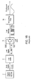
- FIG. 1A illustrates an approach where the digital N-bit sampled signal from a digital source 1 such as a CD player in put directly to a N-bit DAC 2 comprising a resistor network. This gives an intermediate analog signal quantized to 2N voltage levels and sample-and-held at the audio sample rate; which signal is then passed through a low-pass filter 3a to give a smoothed analog waveform.
- a digital source 1 such as a CD player
- N-bit DAC 2 comprising a resistor network
- the DAC 2 needs to have the full resolution of the digital word, so to get say -100 dB distortion, one needs a DAC 2 linear to better than 16 bits, which is difficult and expensive and power-hungry. However, for lower-performance applications, say, telephony, this technique may be appropriate.
- the DAC may comprise a resistor string and selection switches as drawn, or alternatively, an array of selectable parallel current sources, or switched capacitor circuitry as is known.
- FIG. 1B illustrates an alternative scheme.
- the N-bit digital word from the digital source 1 is input to a digital delta-sigma modulator 4, which outputs a single-bit digital stream, at a much higher sample rate, for example 6 MHz.
- the quantization noise introduced is spectrally shaped to move it out of the audio band.
- the DAC 4 now need only be a simple 1-bit DAC, essentially a switch between two voltage levels. Its two level output then requires filtering, but the anti-aliasing requirements are much more relaxed given the higher sample rate, and so a simpler, cheaper filter 3b can be implemented.
- the DAC switches may drive voltages into resistors of the following filters, or control the switching of capacitors in switched-capacitor filters, or may control current sources feeding into following filters.
- FIG. 1C illustrates a further alternative, in which a multi-bit (n-bit) delta-sigma converter 6 is used.
- the multi-bit output has less in-band quantization noise than the single-bit implementation, allowing better performance for a given clock frequency, and is also less sensitive to clock jitter than a 1-bit scheme.
- a resistor network DAC 7 can be used as shown to generate an n-bit sampled analog intermediate signal, though in practical implementations switched-capacitor or switched-current circuitry may be used.
- the intermediate waveform, prior to the smoothing filter 3c, has less out-of-band quantization noise so further easing the requirements on this filter. Because of the higher sample rate, known techniques such as dynamic-element matching can be used to move distortion components due to mismatch of component elements of the n-bit DAC 7 out of the audio band.
- delta-sigma as used here in “delta-sigma modulator” or “delta-sigma converter” or “delta-sigma bit stream” for instance, are taken here to encompass any similar scheme, such as “noise shapers”, which take a lower-sample-rate wide-bit-width data input data stream and output a high-sample-rate small-bit-width data stream, usually but not necessarily shaping the spectrum of the resulting extra quantization noise so that it falls outside the signal band of interest.
- noise shapers which take a lower-sample-rate wide-bit-width data input data stream and output a high-sample-rate small-bit-width data stream, usually but not necessarily shaping the spectrum of the resulting extra quantization noise so that it falls outside the signal band of interest.
- DAC DAC
- filter 3a, 3b, 3c
- the DAC and filter are implemented using CMOS integrated circuit technology.
- the DAC and filter may be implemented using switched-capacitor techniques, although the some or all of the filtering may be implemented just using a CMOS op amp and passive resistors and capacitors, on-chip or off-chip.
- a digital to analog converter includes a first continuous-time stage that receives an input signal associated with a digital signal and performs continuous-time digital-to-analog conversion operations on the input signal.
- the first continuous-time stage outputs a first output signal.
- a second switched-capacitor stage receives the first output signal and performs switched-capacitor filtering of the first output signal.
- the second switched-capacitor stage outputs a continuous analog signal associated with the digital signal.
- a method of forming a digital to analog converter includes providing a first continuous-time stage that receives an input signal associated with a digital signal and performs continuous-time digital-to-analog conversion operations on the input signal.
- the first continuous-time stage outputs a first output signal.
- the method includes providing a second switched-capacitor stage receives the first output signal and performs switched-capacitor filtering of the first output signal.
- the second switched-capacitor stage outputs a continuous analog signal associated with the digital signal.
- a method of performing digital-to-analog conversion includes receiving an input signal associated with a digital signal and performing continuous-time digital-to-analog conversion operations on the input signal. A first output signal is outputted. A switched-capacitor filtering is performed on the first output signal. Also, the method includes outputting a continuous analog signal associated with the digital signal.
- the invention provides a novel approach in addressing difficulties associated with digital to analog conversion.
- the invention incorporates a continuous time filter arrangement with commonly known switched-capacitor architectures to aid in processing data received by digital modulators.
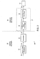
- FIG. 2 is a flowchart overview of the digital-to-analog converter (DAC) 2 used in accordance with the invention.
- the DAC 20 includes two sides, a digital section 35 and an analog section 36, used in performing digital-to-analog conversion.
- a digital signal 38 is received by the DAC 20 through a sigma-delta modulator 22.
- the sigma-delta modulator 22 takes the digital signal 38 having a lower-sample-rate wide-bit-width data and provides an output signal 34 having a high-sample-rate small-bit-width, usually but not necessarily shaping the spectrum of the resulting extra quantization noise so that it falls outside the signal band of interest.
- a scrambler 24 receives the output signal 34 and provides an output signal 37 associated with varying the selection of data units to achieve that level for a given value of the output signal 34.
- the scrambler 24 selects a different combination of data units on a pseudo-random basis, to achieve the desired signal current to drive the analog side 36.
- the analog section 36 includes a second order low pass filter arrangement 27 that comprises a first continuous time stage 26 and a second switched-capacitor stage 30.
- the first continuous time stage 26 receives the output signal 37 and performs filtering using continuous-time circuits commonly used in continuous-time sigma delta modulators.
- the first continuous time stage 26 then outputs an analog signal 31.
- Note such continuous-time architectures can achieve higher signal-to-noise performance in noisy mixed-signal chips, because they are less sensitive to transients and substrate noise.
- the second switched-capacitor stage 30 receives the output signal 31 and performs filtering operations typically performed by switched-capacitor circuits used in sigma delta DACs.
- the second switched-capacitor stage 30 outputs a continuous signal 39 to an output device 32.
- the invention combines the first continuous time stage 26 with a second switched-capacitor stage 30.
- the first continuous time stage 26 achieves higher signal-to-noise performance than would be practical with an all-switched-capacitor design.
- An all-switched-capacitor architecture would be more sensitive to transients and substrate noise. This makes it difficult to improve their signal-to-noise ratio performance when they are used in a mixed signal chip that includes digital circuitry.
- the second switched-capacitor stage 30 adds additional low-pass filtering with less cost and area than the first continuous time stage 26.
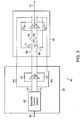
- FIG. 3 shows is a schematic diagram illustrating the details of the inventive second order filter arrangement used in accordance with the invention.
- the first continuous-time stage 42 includes a switched current source 46 used to drive the inverting and non-inverting input nodes of an amplifier A2.
- the switched current source 46 receives as input the signal 64 produced by a scrambler as described in FIG. 2 and provides two output signals 66 and 68. Based on the input signal 64 the switched current source 46 dictates the charging of the respective capacitors C1 and C2.
- Note output signal 66 is coupled to the inverting input node of the operational amplifier A2 and switch 68 is coupled to the non-inverting input node of the operational amplifier A2.
- the capacitor C1 is coupled to both the inverting input node and the non-inverting output node of the operational amplifier A2.
- the resistor R4 is coupled to the inverting input node of the operational amplifier A2.
- the capacitor C2 is coupled to both the non-inverting input node and the inverting output node of the operational amplifier A2.
- the resistor R3 is coupled to the non-inverting input node of the operational amplifier A2.
- the second switched-capacitor stage 44 receives as input the inverting and non-inverting output nodes of operational amplifier A2.
- Switches 66 and 68 are coupled to the non-inverting and inverting output nodes of operational amplifier A2.
- a capacitor C3 is coupled to the switch 66 and a capacitor C4 is coupled to the switch 68.
- switches 66 and 68 are open or closed based in part by the signals they receive. Also, when the switches 66 and 68 are closed both capacitors C3 and C4 are charged accordingly until their respective switches 66 and 68 are opened and they discharge. However, the switches 66 and 68 are never simultaneously open or closed at the same time.
- the capacitor C3 is coupled to the inverting input node of an operational amplifier A3 via switch 56.
- a charging capacitor C5 is coupled at both the inverting input node and the non-inverting output node of the operational amplifier A3.
- the other end of resistor R4 is coupled to the non-inverting output node of the operational amplifier A3.
- the capacitor C4 is coupled to the inverting input node of an amplifier A3 via switch 58.
- a charging capacitor C6 is coupled at both the non-inverting input node and the inverting output node of the operational amplifier A3.
- the other end of resistor R3 is coupled to the inverting output node of the operational amplifier A3.
- a group of switches 5 are placed at various locations in the second switched-capacitor stage 44. These groups of switches 5 receive a clock signal CLK which dictates when these switches are opened and closed simultaneously.
- switches 5, 52, 54, 56, 58, 66, and 68 receive respective clock signals those determine when these respective switches will open or close.
- the resistors R3 and R4 are also positioned to provide an RC filter arrangement at the first time-continuous stage 42 and aid in providing a stable continuous signal 74 as output by the operational amplifier A3.
- the invention provides a novel approach in performing digital-to-analog conversion by introducing a two stage low pass filter arrangement having both continuous-time and switched-capacitor architectures. Moreover, the invention increases the signal-to-noise ratio performance that would be practical with an all-switched-capacitor design and provides an additional low-pass filtering with less cost and area than a conventional continuous-time design.
Landscapes
- Engineering & Computer Science (AREA)
- Theoretical Computer Science (AREA)
- Power Engineering (AREA)
- Analogue/Digital Conversion (AREA)
- Compression, Expansion, Code Conversion, And Decoders (AREA)
- Filters That Use Time-Delay Elements (AREA)
- Arrangements For Transmission Of Measured Signals (AREA)
Claims (19)
- Digital-zu-Analog-Konverter (20) aufweisend:eine erste zeitkontinuierliche Stufe (26) zum Empfangen eines Eingangssignals (37) assoziiert mit einem digitalen Signal und zum Durchführen von zeitkontinuierlicher Digital-zu-Analog-Konvertierungsoperationen auf besagtem Eingangssignal (37), wobei die besagte zeitkontinuierliche Stufe (26) angepasst ist zum Ausgeben eines ersten Ausgangssignals (31);dadurch gekennzeichnet,
dass der Konverter weiter aufweist:eine zweite Schaltkondensatorstufe (30) zum Empfangen des besagten ersten Ausgangssignals (31) und Schaltkondensatorfilterung auf dem besagten ersten Ausgangssignal (31) durchführt, wobei die besagte zweite Schaltkondensatorstufe (30) angepasst ist zum Ausgeben eines kontinuierlichen Analogsignals (39) assoziiert mit dem besagten digitalen Signal. - Digital-zu-Analog-Konverter (20) gemäß Anspruch 1, wobei die besagte erste zeitkontinuierliche Stufe (26) und die besagte zweite Schaltkondensatorstufe (30) eine zweiter-Ordnung-Tiefpassfilteranordnung (27) aufweisen.
- Digital-zu-Analog-Konverter (20) nach Anspruch 1, weiter aufweisend einen digitalen Modulator (22), der das besagte digitale Signal, welches eine niedrige-Abtastrate weite-Bit-Weitendaten (38) hat, empfängt und ein drittes Ausgangssignal (34), welches eine hohe-Abtastrate kleine-Bit-Weite hat, zur Verfügung stellt.
- Digital-zu-Analog-Konverter (20) nach Anspruch 3, weiter aufweisend einen Verwürfler (24), welcher das besagte dritte Ausgangssignal (34) empfängt und ein viertes Ausgangssignal (37) durch Auswählen einer unterschiedlichen Kombination von Dateneinheiten auf einer Pseudo-Zufallsbasis ausgibt, um den erwünschten Signalstrom zum Betreiben der ersten zeitkontinuierlichen Stufe (26) zu erzielen.
- Digital-zu-Analog-Konverter (20) nach Anspruch 3, wobei der besagte digitale Modulator (22) einen Sigma-Delta-Modulator aufweist.
- Digital-zu-Analog-Konverter (20) nach Anspruch 1, wobei die besagte erste kontinuierliche Stufe (26) eine Vielzahl von RC-Filteranordnungen aufweist.
- Digital-zu-Analog-Konverter (20) nach Anspruch 1, wobei die besagte zweite Schaltkondensatorstufe (30) eine Schaltkreisanordnung aufweist, wo eine Vielzahl von Kondensatoren zum Laden und Entladen ihrer entsprechenden Ladungen angeordnet sind.
- Digital-zu-Analog-Konverter (20) nach Anspruch 6, wobei die besagte erste kontinuierliche Stufe (26) einen Operationsverstärker zum Betreiben der besagten RC-Filteranordnungen aufweist.
- Digital-zu-Analog-Konverter (20) nach Anspruch 7, wobei die besagte zweite Schaltkondensatorstufe (30) einen Operationsverstärker aufweist, um beim Laden und Entladen der besagten Kondensatoren zu helfen.
- Verfahren zum Bilden eines Digital-zu-Analog-Konverters (20) aufweisend:Zurverfügungstellen einer ersten zeitkontinuierlichen Stufe (26), welche ein Eingangssignal (37) assoziiert mit einem digitalen Signal empfängt und zeitkontinuierliche Digital-zu-Analog-Konverterierungsoperationen auf dem besagten Eingangssignal (37) durchführt, wobei die besagte erste zeitkontinuierliche Stufe (26) ein erstes Ausgangssignal (31) ausgibt;dadurch gekennzeichnet, dass das Verfahren weiter aufweist:Zurverfügungstellen einer zweiten Schaltkondensatorstufe (30), welche das erste Ausgangssignal (31) empfängt und Schaltkondensatorfilterung auf dem besagten Ausgangssignal (31) durchführt, wobei die besagte zweite Schaltkondensatorstufe (30) ein kontinuierliches Analogsignal (39) assoziiert mit dem besagten digitalen Signal ausgibt.
- Verfahren nach Anspruch 10, wobei die besagte erste zeitkontinuierliche Stufe (26) und die besagte zweite Schalkondensatorstufe (30) eine zweiter-Ordnung-Tiefpassfilter-Anordnung aufweisen.
- Verfahren nach Anspruch 10, weiter aufweisend einen digitalen Modulator (22), welcher das besagte digitale Signal, welches eine niedrige-Abtastrate weite-Bit-Weiten Daten (38) hat, empfängt und ein drittes Ausgangssignal (34) bereitstellt, welches eine hohe-Abtastrate kleine-Bit Weite hat.
- Verfahren nach Anspruch 12, weiter aufweisend einen Verwürfler (24), welcher das besagte dritte Ausgangssignal (34) empfängt und ein viertes Ausgangssignal (37) durch Auswählen einer unterschiedlichen Kombination von Dateneinheiten auf einer Pseudo-Zufallsbasis ausgibt, um den erwünschten Signalstrom zum Betreiben der ersten zeitkontinuierlichen Stufe (26) zu erzielen.
- Verfahren nach Anspruch 12, wobei der besagte digitale Modulator (22) einen Sigma-Delta-Modulator aufweist.
- Verfahren nach Anspruch 10, wobei die besagte erste kontinuierliche Stufe (26) eine Vielzahl von RC-Filteranordnungen aufweist.
- Verfahren nach Anspruch 10, wobei die besagte zweite Schaltkondensatorstufe (30) eine Schaltkreisanordnung aufweist, wo eine Vielzahl von Kondensatoren zum Laden und Entladen ihrer entsprechenden Ladungen angeordnet sind.
- Verfahren nach Anspruch 15, wobei die besagte erste kontinuierliche Stufe (26) einen Operationsverstärker zum Betreiben der besagten RC-Filteranordnung aufweist.
- Verfahren nach Anspruch 16, wobei die besagte zweite Schaltkondensatorstufe (30) einen Operationsverstärker aufweist, um beim Laden und Entladen der besagten Kondensatoren zu helfen.
- Verfahren zur Durchführung von Digital-zu-Analog-Konvertierung aufweisend:Empfangen eines Eingangssignals (37) assoziiert mit einem digitalen Signal;Durchführung von zeitkontinuierliche Digital-zu-Analog-Konvertierungsoperationen auf dem besagten Eingangssignal (37);Ausgeben eines ersten Ausgangssignal (31);dadurch gekennzeichnet, dass das Verfahren weiter aufweist:Durchführen von Schaltkondensatorfilterung auf dem besagten ersten Ausgangssignal (31); undAusgeben eines kontinuierlichen Analogsignals (39) assoziiert mit dem besagten digitalen Signal.
Applications Claiming Priority (2)
| Application Number | Priority Date | Filing Date | Title |
|---|---|---|---|
| US75440505P | 2005-12-28 | 2005-12-28 | |
| PCT/US2006/049326 WO2007079097A2 (en) | 2005-12-28 | 2006-12-27 | Architecture combining a continuous-time stage with a switched-capacitor stage for digital-to-analog converters and low-pass filters |
Publications (2)
| Publication Number | Publication Date |
|---|---|
| EP1966894A2 EP1966894A2 (de) | 2008-09-10 |
| EP1966894B1 true EP1966894B1 (de) | 2010-02-10 |
Family
ID=38094435
Family Applications (1)
| Application Number | Title | Priority Date | Filing Date |
|---|---|---|---|
| EP06848190A Active EP1966894B1 (de) | 2005-12-28 | 2006-12-27 | Architektur zur kombination eines zeitkontinuierlichen status mit einem schaltkondensatorstatus für digital-analog-wandler und tiefpassfilter |
Country Status (7)
| Country | Link |
|---|---|
| US (1) | US7423573B2 (de) |
| EP (1) | EP1966894B1 (de) |
| JP (1) | JP4747199B2 (de) |
| CN (1) | CN101351967B (de) |
| AT (1) | ATE457550T1 (de) |
| DE (1) | DE602006012226D1 (de) |
| WO (1) | WO2007079097A2 (de) |
Families Citing this family (17)
| Publication number | Priority date | Publication date | Assignee | Title |
|---|---|---|---|---|
| US8009995B2 (en) * | 2006-01-12 | 2011-08-30 | The United States Of America As Represented By The Secretary Of The Navy | Method and apparatus for photonic digital-to-analog conversion |
| US7903011B2 (en) * | 2006-09-13 | 2011-03-08 | Honeywell International Inc. | Differential current-mode translator in a sigma-delta digital-to-analog converter |
| JP4470996B2 (ja) * | 2007-12-25 | 2010-06-02 | セイコーエプソン株式会社 | A/d変換回路及び電子機器 |
| US7782237B2 (en) * | 2008-06-13 | 2010-08-24 | The Board Of Trustees Of The Leland Stanford Junior University | Semiconductor sensor circuit arrangement |
| US7956782B2 (en) * | 2009-06-11 | 2011-06-07 | Honeywell International Inc. | Current-mode sigma-delta digital-to-analog converter |
| US8446191B2 (en) * | 2009-12-07 | 2013-05-21 | Qualcomm Incorporated | Phase locked loop with digital compensation for analog integration |
| US8339165B2 (en) | 2009-12-07 | 2012-12-25 | Qualcomm Incorporated | Configurable digital-analog phase locked loop |
| US8441383B1 (en) * | 2011-03-11 | 2013-05-14 | Rockwell Collins, Inc. | Photonic digital-to-analog conversion (DAC) based on RSOAs |
| US8810443B2 (en) * | 2012-04-20 | 2014-08-19 | Linear Technology Corporation | Analog-to-digital converter system and method |
| JP5935519B2 (ja) * | 2012-06-05 | 2016-06-15 | 住友電気工業株式会社 | Δς変調システム |
| FR3042928B1 (fr) * | 2015-10-21 | 2018-11-30 | Thales Sa | Dispositif de generation de signaux analogiques et utilisation associee |
| CN105763170B (zh) * | 2016-03-28 | 2018-09-18 | 浙江涵普电力科技有限公司 | 一种电力信号数字滤波方法 |
| CN105743462A (zh) * | 2016-03-28 | 2016-07-06 | 浙江涵普电力科技有限公司 | 测量响应时间可调的电力信号数字滤波方法 |
| US9979445B2 (en) | 2016-07-15 | 2018-05-22 | Futurewei Technologies, Inc. | Digital to analog converter apparatus, system, and method with quantization noise that is independent of an input signal |
| CN106452387A (zh) * | 2016-08-31 | 2017-02-22 | 安徽赛福电子有限公司 | 一种基于开关电容的可配置多模滤波器 |
| US11165414B2 (en) | 2019-12-20 | 2021-11-02 | Infineon Technologies Ag | Reconfigurable filter network with shortened settling time |
| CN114337674A (zh) * | 2020-10-09 | 2022-04-12 | 博通集成电路(上海)股份有限公司 | 一种内嵌低通滤波器的数模转换器 |
Family Cites Families (14)
| Publication number | Priority date | Publication date | Assignee | Title |
|---|---|---|---|---|
| FR2642921B1 (fr) * | 1989-02-07 | 1991-05-17 | Texas Instruments France | Chaine de conversion numerique-analogique incluant un modulateur numerique a plusieurs niveaux de quantification, associe a un convertisseur numerique-analogique |
| US5245344A (en) * | 1991-01-15 | 1993-09-14 | Crystal Semiconductor | High order switched-capacitor filter with dac input |
| US5412387A (en) * | 1993-04-06 | 1995-05-02 | Analog Devices, Inc. | Error reduction in switched capacitor digital-to-analog converter systems by balanced sampling |
| JP3282510B2 (ja) * | 1996-08-01 | 2002-05-13 | ヤマハ株式会社 | D/aコンバータ回路 |
| JP3885911B2 (ja) * | 1997-11-18 | 2007-02-28 | 旭化成マイクロシステム株式会社 | D/a変換器 |
| US6118399A (en) * | 1998-03-30 | 2000-09-12 | Silicon Laboratories, Inc. | Coarse/fine switching on digital-to-analog conversion output |
| US6087969A (en) * | 1998-04-27 | 2000-07-11 | Motorola, Inc. | Sigma-delta modulator and method for digitizing a signal |
| US6873278B1 (en) * | 2000-05-21 | 2005-03-29 | Analog Devices, Inc. | Method and apparatus for use in switched capacitor systems |
| US6522277B2 (en) * | 2001-02-05 | 2003-02-18 | Asahi Kasei Microsystems, Inc. | Circuit, system and method for performing dynamic element matching using bi-directional rotation within a data converter |
| EP1573420A4 (de) * | 2001-07-13 | 2006-11-15 | Cirrus Logic Inc | Schaltungen, systeme und verfahren zur lautstärkeregelung in 1-bit-digital-audiosystemen |
| JP2003298424A (ja) * | 2002-04-05 | 2003-10-17 | Matsushita Electric Ind Co Ltd | 信号処理装置およびd/a変換器 |
| JP3978744B2 (ja) * | 2002-07-25 | 2007-09-19 | パイオニア株式会社 | デジタルアナログ変換器 |
| US6861968B2 (en) * | 2003-01-21 | 2005-03-01 | Cirrus Logic, Inc. | Signal processing system with baseband noise modulation and noise filtering |
| US6870494B1 (en) * | 2003-10-01 | 2005-03-22 | C-Media Electronics Inc. | System of multi-channel shared resistor-string digital-to-analog converters and method of the same |
-
2006
- 2006-12-27 DE DE602006012226T patent/DE602006012226D1/de active Active
- 2006-12-27 WO PCT/US2006/049326 patent/WO2007079097A2/en not_active Ceased
- 2006-12-27 AT AT06848190T patent/ATE457550T1/de not_active IP Right Cessation
- 2006-12-27 US US11/616,468 patent/US7423573B2/en active Active
- 2006-12-27 JP JP2008548691A patent/JP4747199B2/ja not_active Expired - Fee Related
- 2006-12-27 CN CN2006800499916A patent/CN101351967B/zh active Active
- 2006-12-27 EP EP06848190A patent/EP1966894B1/de active Active
Also Published As
| Publication number | Publication date |
|---|---|
| JP2009522874A (ja) | 2009-06-11 |
| CN101351967B (zh) | 2012-05-30 |
| US7423573B2 (en) | 2008-09-09 |
| EP1966894A2 (de) | 2008-09-10 |
| ATE457550T1 (de) | 2010-02-15 |
| CN101351967A (zh) | 2009-01-21 |
| US20070159370A1 (en) | 2007-07-12 |
| WO2007079097A3 (en) | 2007-08-23 |
| DE602006012226D1 (de) | 2010-03-25 |
| WO2007079097A2 (en) | 2007-07-12 |
| JP4747199B2 (ja) | 2011-08-17 |
Similar Documents
| Publication | Publication Date | Title |
|---|---|---|
| US7102557B1 (en) | Switched capacitor DAC | |
| EP1966894B1 (de) | Architektur zur kombination eines zeitkontinuierlichen status mit einem schaltkondensatorstatus für digital-analog-wandler und tiefpassfilter | |
| US6816097B2 (en) | System and method for performing digital-to-analog conversion using a sigma-delta modulator | |
| Sarhang-Nejad et al. | A high-resolution multibit sigma delta ADC with digital correction and relaxed amplifier requirements | |
| Fujimori et al. | A multibit delta-sigma audio DAC with 120-dB dynamic range | |
| US7446686B2 (en) | Incremental delta-sigma data converters with improved stability over wide input voltage ranges | |
| US20120242521A1 (en) | Method and circuit for continuous-time delta-sigma dac with reduced noise | |
| US7515079B2 (en) | Method of controlling delta-sigma modulator and delta-sigma modulator | |
| JP6767715B2 (ja) | Ad変換器 | |
| JPH04229723A (ja) | 高次シグマ・デルタアナログ/デジタル変換器 | |
| CN107508600B (zh) | 用于具有并联耦接的积分器的δσadc的方法和设备 | |
| CN111697971A (zh) | Δ-σ模数转换器以及用于操作δ-σ模数转换器的方法 | |
| US9252801B2 (en) | Sigma-delta converter system and method | |
| JP4331188B2 (ja) | デジタル/アナログ変換器および信号のデジタル/アナログ変換方法 | |
| US7388533B2 (en) | Multi-bit sigma-delta modulator and digital-to-analog converter with one digital-to-analog capacitor | |
| Colonna et al. | A 0.22-mm/sup 2/7.25-mW per-channel audio stereo-DAC with 97-dB DR and 39-dB SNR/sub out | |
| Yang et al. | A 114 dB 68 mW chopper-stabilized stereo multi-bit audio A/D converter | |
| Gong et al. | A 120 dB multi-bit SC audio DAC with second-order noise shaping | |
| KR100766073B1 (ko) | 단일 dac 캐패시터를 이용한 멀티 비트 시그마 델타변조기 및 디지털 아날로그 변환기 | |
| Subramanian et al. | A 119-dBA Dynamic Range, 3.3-mW Audio CTDSM With a Class-B Resistor DAC and Continuous-Time Quantizer | |
| JP3074301B2 (ja) | 向上したオ―バサンプリングシグマ―デルタ変調器 | |
| Dijkmans et al. | Sigma-Delta versus Binary Weighted AD/DA conversion, what is the most promising? | |
| O'Connell et al. | A novel noise efficient feedback DAC within a switched capacitor/spl Sigma//spl Delta/ADC | |
| Fiez et al. | Delta-sigma A/D converters: the next generation | |
| Lee | High efficiency delta-sigma modulation data converters |
Legal Events
| Date | Code | Title | Description |
|---|---|---|---|
| PUAI | Public reference made under article 153(3) epc to a published international application that has entered the european phase |
Free format text: ORIGINAL CODE: 0009012 |
|
| 17P | Request for examination filed |
Effective date: 20080618 |
|
| AK | Designated contracting states |
Kind code of ref document: A2 Designated state(s): AT BE BG CH CY CZ DE DK EE ES FI FR GB GR HU IE IS IT LI LT LU LV MC NL PL PT RO SE SI SK TR |
|
| 17Q | First examination report despatched |
Effective date: 20081107 |
|
| GRAP | Despatch of communication of intention to grant a patent |
Free format text: ORIGINAL CODE: EPIDOSNIGR1 |
|
| RIC1 | Information provided on ipc code assigned before grant |
Ipc: H03H 19/00 20060101AFI20090703BHEP Ipc: H03M 3/00 20060101ALI20090703BHEP Ipc: H03M 7/00 20060101ALI20090703BHEP |
|
| DAX | Request for extension of the european patent (deleted) | ||
| GRAS | Grant fee paid |
Free format text: ORIGINAL CODE: EPIDOSNIGR3 |
|
| GRAA | (expected) grant |
Free format text: ORIGINAL CODE: 0009210 |
|
| AK | Designated contracting states |
Kind code of ref document: B1 Designated state(s): AT BE BG CH CY CZ DE DK EE ES FI FR GB GR HU IE IS IT LI LT LU LV MC NL PL PT RO SE SI SK TR |
|
| REG | Reference to a national code |
Ref country code: GB Ref legal event code: FG4D |
|
| REG | Reference to a national code |
Ref country code: CH Ref legal event code: EP |
|
| REG | Reference to a national code |
Ref country code: IE Ref legal event code: FG4D |
|
| REF | Corresponds to: |
Ref document number: 602006012226 Country of ref document: DE Date of ref document: 20100325 Kind code of ref document: P |
|
| REG | Reference to a national code |
Ref country code: NL Ref legal event code: VDEP Effective date: 20100210 |
|
| LTIE | Lt: invalidation of european patent or patent extension |
Effective date: 20100210 |
|
| PG25 | Lapsed in a contracting state [announced via postgrant information from national office to epo] |
Ref country code: ES Free format text: LAPSE BECAUSE OF FAILURE TO SUBMIT A TRANSLATION OF THE DESCRIPTION OR TO PAY THE FEE WITHIN THE PRESCRIBED TIME-LIMIT Effective date: 20100521 Ref country code: PT Free format text: LAPSE BECAUSE OF FAILURE TO SUBMIT A TRANSLATION OF THE DESCRIPTION OR TO PAY THE FEE WITHIN THE PRESCRIBED TIME-LIMIT Effective date: 20100611 Ref country code: IS Free format text: LAPSE BECAUSE OF FAILURE TO SUBMIT A TRANSLATION OF THE DESCRIPTION OR TO PAY THE FEE WITHIN THE PRESCRIBED TIME-LIMIT Effective date: 20100610 Ref country code: LT Free format text: LAPSE BECAUSE OF FAILURE TO SUBMIT A TRANSLATION OF THE DESCRIPTION OR TO PAY THE FEE WITHIN THE PRESCRIBED TIME-LIMIT Effective date: 20100210 |
|
| PG25 | Lapsed in a contracting state [announced via postgrant information from national office to epo] |
Ref country code: PL Free format text: LAPSE BECAUSE OF FAILURE TO SUBMIT A TRANSLATION OF THE DESCRIPTION OR TO PAY THE FEE WITHIN THE PRESCRIBED TIME-LIMIT Effective date: 20100210 Ref country code: AT Free format text: LAPSE BECAUSE OF FAILURE TO SUBMIT A TRANSLATION OF THE DESCRIPTION OR TO PAY THE FEE WITHIN THE PRESCRIBED TIME-LIMIT Effective date: 20100210 Ref country code: FI Free format text: LAPSE BECAUSE OF FAILURE TO SUBMIT A TRANSLATION OF THE DESCRIPTION OR TO PAY THE FEE WITHIN THE PRESCRIBED TIME-LIMIT Effective date: 20100210 Ref country code: LV Free format text: LAPSE BECAUSE OF FAILURE TO SUBMIT A TRANSLATION OF THE DESCRIPTION OR TO PAY THE FEE WITHIN THE PRESCRIBED TIME-LIMIT Effective date: 20100210 Ref country code: SI Free format text: LAPSE BECAUSE OF FAILURE TO SUBMIT A TRANSLATION OF THE DESCRIPTION OR TO PAY THE FEE WITHIN THE PRESCRIBED TIME-LIMIT Effective date: 20100210 |
|
| PG25 | Lapsed in a contracting state [announced via postgrant information from national office to epo] |
Ref country code: CY Free format text: LAPSE BECAUSE OF FAILURE TO SUBMIT A TRANSLATION OF THE DESCRIPTION OR TO PAY THE FEE WITHIN THE PRESCRIBED TIME-LIMIT Effective date: 20100210 Ref country code: NL Free format text: LAPSE BECAUSE OF FAILURE TO SUBMIT A TRANSLATION OF THE DESCRIPTION OR TO PAY THE FEE WITHIN THE PRESCRIBED TIME-LIMIT Effective date: 20100210 Ref country code: RO Free format text: LAPSE BECAUSE OF FAILURE TO SUBMIT A TRANSLATION OF THE DESCRIPTION OR TO PAY THE FEE WITHIN THE PRESCRIBED TIME-LIMIT Effective date: 20100210 Ref country code: SE Free format text: LAPSE BECAUSE OF FAILURE TO SUBMIT A TRANSLATION OF THE DESCRIPTION OR TO PAY THE FEE WITHIN THE PRESCRIBED TIME-LIMIT Effective date: 20100210 Ref country code: EE Free format text: LAPSE BECAUSE OF FAILURE TO SUBMIT A TRANSLATION OF THE DESCRIPTION OR TO PAY THE FEE WITHIN THE PRESCRIBED TIME-LIMIT Effective date: 20100210 Ref country code: GR Free format text: LAPSE BECAUSE OF FAILURE TO SUBMIT A TRANSLATION OF THE DESCRIPTION OR TO PAY THE FEE WITHIN THE PRESCRIBED TIME-LIMIT Effective date: 20100511 Ref country code: BE Free format text: LAPSE BECAUSE OF FAILURE TO SUBMIT A TRANSLATION OF THE DESCRIPTION OR TO PAY THE FEE WITHIN THE PRESCRIBED TIME-LIMIT Effective date: 20100210 |
|
| PG25 | Lapsed in a contracting state [announced via postgrant information from national office to epo] |
Ref country code: BG Free format text: LAPSE BECAUSE OF FAILURE TO SUBMIT A TRANSLATION OF THE DESCRIPTION OR TO PAY THE FEE WITHIN THE PRESCRIBED TIME-LIMIT Effective date: 20100510 Ref country code: SK Free format text: LAPSE BECAUSE OF FAILURE TO SUBMIT A TRANSLATION OF THE DESCRIPTION OR TO PAY THE FEE WITHIN THE PRESCRIBED TIME-LIMIT Effective date: 20100210 Ref country code: CZ Free format text: LAPSE BECAUSE OF FAILURE TO SUBMIT A TRANSLATION OF THE DESCRIPTION OR TO PAY THE FEE WITHIN THE PRESCRIBED TIME-LIMIT Effective date: 20100210 |
|
| PLBE | No opposition filed within time limit |
Free format text: ORIGINAL CODE: 0009261 |
|
| STAA | Information on the status of an ep patent application or granted ep patent |
Free format text: STATUS: NO OPPOSITION FILED WITHIN TIME LIMIT |
|
| 26N | No opposition filed |
Effective date: 20101111 |
|
| PG25 | Lapsed in a contracting state [announced via postgrant information from national office to epo] |
Ref country code: DK Free format text: LAPSE BECAUSE OF FAILURE TO SUBMIT A TRANSLATION OF THE DESCRIPTION OR TO PAY THE FEE WITHIN THE PRESCRIBED TIME-LIMIT Effective date: 20100210 |
|
| PG25 | Lapsed in a contracting state [announced via postgrant information from national office to epo] |
Ref country code: IT Free format text: LAPSE BECAUSE OF FAILURE TO SUBMIT A TRANSLATION OF THE DESCRIPTION OR TO PAY THE FEE WITHIN THE PRESCRIBED TIME-LIMIT Effective date: 20100210 |
|
| PG25 | Lapsed in a contracting state [announced via postgrant information from national office to epo] |
Ref country code: MC Free format text: LAPSE BECAUSE OF NON-PAYMENT OF DUE FEES Effective date: 20101231 |
|
| REG | Reference to a national code |
Ref country code: CH Ref legal event code: PL |
|
| PG25 | Lapsed in a contracting state [announced via postgrant information from national office to epo] |
Ref country code: IE Free format text: LAPSE BECAUSE OF NON-PAYMENT OF DUE FEES Effective date: 20101227 Ref country code: CH Free format text: LAPSE BECAUSE OF NON-PAYMENT OF DUE FEES Effective date: 20101231 Ref country code: LI Free format text: LAPSE BECAUSE OF NON-PAYMENT OF DUE FEES Effective date: 20101231 |
|
| PG25 | Lapsed in a contracting state [announced via postgrant information from national office to epo] |
Ref country code: HU Free format text: LAPSE BECAUSE OF FAILURE TO SUBMIT A TRANSLATION OF THE DESCRIPTION OR TO PAY THE FEE WITHIN THE PRESCRIBED TIME-LIMIT Effective date: 20100811 Ref country code: LU Free format text: LAPSE BECAUSE OF NON-PAYMENT OF DUE FEES Effective date: 20101227 |
|
| PG25 | Lapsed in a contracting state [announced via postgrant information from national office to epo] |
Ref country code: TR Free format text: LAPSE BECAUSE OF FAILURE TO SUBMIT A TRANSLATION OF THE DESCRIPTION OR TO PAY THE FEE WITHIN THE PRESCRIBED TIME-LIMIT Effective date: 20100210 |
|
| REG | Reference to a national code |
Ref country code: FR Ref legal event code: PLFP Year of fee payment: 10 |
|
| REG | Reference to a national code |
Ref country code: FR Ref legal event code: PLFP Year of fee payment: 11 |
|
| PGFP | Annual fee paid to national office [announced via postgrant information from national office to epo] |
Ref country code: FR Payment date: 20161111 Year of fee payment: 11 Ref country code: GB Payment date: 20161221 Year of fee payment: 11 |
|
| GBPC | Gb: european patent ceased through non-payment of renewal fee |
Effective date: 20171227 |
|
| REG | Reference to a national code |
Ref country code: FR Ref legal event code: ST Effective date: 20180831 |
|
| PG25 | Lapsed in a contracting state [announced via postgrant information from national office to epo] |
Ref country code: FR Free format text: LAPSE BECAUSE OF NON-PAYMENT OF DUE FEES Effective date: 20180102 |
|
| PG25 | Lapsed in a contracting state [announced via postgrant information from national office to epo] |
Ref country code: GB Free format text: LAPSE BECAUSE OF NON-PAYMENT OF DUE FEES Effective date: 20171227 |
|
| PGFP | Annual fee paid to national office [announced via postgrant information from national office to epo] |
Ref country code: DE Payment date: 20251126 Year of fee payment: 20 |