EP1964094B1 - Verfahren zur steuerung eines anzeigeschirms durch kapazitive kopplung - Google Patents
Verfahren zur steuerung eines anzeigeschirms durch kapazitive kopplung Download PDFInfo
- Publication number
- EP1964094B1 EP1964094B1 EP06841466A EP06841466A EP1964094B1 EP 1964094 B1 EP1964094 B1 EP 1964094B1 EP 06841466 A EP06841466 A EP 06841466A EP 06841466 A EP06841466 A EP 06841466A EP 1964094 B1 EP1964094 B1 EP 1964094B1
- Authority
- EP
- European Patent Office
- Prior art keywords
- voltage
- electrode
- pol
- prog
- control
- Prior art date
- Legal status (The legal status is an assumption and is not a legal conclusion. Google has not performed a legal analysis and makes no representation as to the accuracy of the status listed.)
- Ceased
Links
Images

Classifications
-
- G—PHYSICS
- G09—EDUCATION; CRYPTOGRAPHY; DISPLAY; ADVERTISING; SEALS
- G09G—ARRANGEMENTS OR CIRCUITS FOR CONTROL OF INDICATING DEVICES USING STATIC MEANS TO PRESENT VARIABLE INFORMATION
- G09G3/00—Control arrangements or circuits, of interest only in connection with visual indicators other than cathode-ray tubes
- G09G3/20—Control arrangements or circuits, of interest only in connection with visual indicators other than cathode-ray tubes for presentation of an assembly of a number of characters, e.g. a page, by composing the assembly by combination of individual elements arranged in a matrix no fixed position being assigned to or needed to be assigned to the individual characters or partial characters
- G09G3/22—Control arrangements or circuits, of interest only in connection with visual indicators other than cathode-ray tubes for presentation of an assembly of a number of characters, e.g. a page, by composing the assembly by combination of individual elements arranged in a matrix no fixed position being assigned to or needed to be assigned to the individual characters or partial characters using controlled light sources
- G09G3/30—Control arrangements or circuits, of interest only in connection with visual indicators other than cathode-ray tubes for presentation of an assembly of a number of characters, e.g. a page, by composing the assembly by combination of individual elements arranged in a matrix no fixed position being assigned to or needed to be assigned to the individual characters or partial characters using controlled light sources using electroluminescent panels
- G09G3/32—Control arrangements or circuits, of interest only in connection with visual indicators other than cathode-ray tubes for presentation of an assembly of a number of characters, e.g. a page, by composing the assembly by combination of individual elements arranged in a matrix no fixed position being assigned to or needed to be assigned to the individual characters or partial characters using controlled light sources using electroluminescent panels semiconductive, e.g. using light-emitting diodes [LED]
- G09G3/3208—Control arrangements or circuits, of interest only in connection with visual indicators other than cathode-ray tubes for presentation of an assembly of a number of characters, e.g. a page, by composing the assembly by combination of individual elements arranged in a matrix no fixed position being assigned to or needed to be assigned to the individual characters or partial characters using controlled light sources using electroluminescent panels semiconductive, e.g. using light-emitting diodes [LED] organic, e.g. using organic light-emitting diodes [OLED]
- G09G3/3225—Control arrangements or circuits, of interest only in connection with visual indicators other than cathode-ray tubes for presentation of an assembly of a number of characters, e.g. a page, by composing the assembly by combination of individual elements arranged in a matrix no fixed position being assigned to or needed to be assigned to the individual characters or partial characters using controlled light sources using electroluminescent panels semiconductive, e.g. using light-emitting diodes [LED] organic, e.g. using organic light-emitting diodes [OLED] using an active matrix
- G09G3/3233—Control arrangements or circuits, of interest only in connection with visual indicators other than cathode-ray tubes for presentation of an assembly of a number of characters, e.g. a page, by composing the assembly by combination of individual elements arranged in a matrix no fixed position being assigned to or needed to be assigned to the individual characters or partial characters using controlled light sources using electroluminescent panels semiconductive, e.g. using light-emitting diodes [LED] organic, e.g. using organic light-emitting diodes [OLED] using an active matrix with pixel circuitry controlling the current through the light-emitting element
-
- G—PHYSICS
- G09—EDUCATION; CRYPTOGRAPHY; DISPLAY; ADVERTISING; SEALS
- G09G—ARRANGEMENTS OR CIRCUITS FOR CONTROL OF INDICATING DEVICES USING STATIC MEANS TO PRESENT VARIABLE INFORMATION
- G09G2300/00—Aspects of the constitution of display devices
- G09G2300/08—Active matrix structure, i.e. with use of active elements, inclusive of non-linear two terminal elements, in the pixels together with light emitting or modulating elements
- G09G2300/0809—Several active elements per pixel in active matrix panels
- G09G2300/0842—Several active elements per pixel in active matrix panels forming a memory circuit, e.g. a dynamic memory with one capacitor
- G09G2300/0852—Several active elements per pixel in active matrix panels forming a memory circuit, e.g. a dynamic memory with one capacitor being a dynamic memory with more than one capacitor
-
- G—PHYSICS
- G09—EDUCATION; CRYPTOGRAPHY; DISPLAY; ADVERTISING; SEALS
- G09G—ARRANGEMENTS OR CIRCUITS FOR CONTROL OF INDICATING DEVICES USING STATIC MEANS TO PRESENT VARIABLE INFORMATION
- G09G2300/00—Aspects of the constitution of display devices
- G09G2300/08—Active matrix structure, i.e. with use of active elements, inclusive of non-linear two terminal elements, in the pixels together with light emitting or modulating elements
- G09G2300/0876—Supplementary capacities in pixels having special driving circuits and electrodes instead of being connected to common electrode or ground; Use of additional capacitively coupled compensation electrodes
-
- G—PHYSICS
- G09—EDUCATION; CRYPTOGRAPHY; DISPLAY; ADVERTISING; SEALS
- G09G—ARRANGEMENTS OR CIRCUITS FOR CONTROL OF INDICATING DEVICES USING STATIC MEANS TO PRESENT VARIABLE INFORMATION
- G09G2310/00—Command of the display device
- G09G2310/02—Addressing, scanning or driving the display screen or processing steps related thereto
- G09G2310/0243—Details of the generation of driving signals
- G09G2310/0254—Control of polarity reversal in general, other than for liquid crystal displays
-
- G—PHYSICS
- G09—EDUCATION; CRYPTOGRAPHY; DISPLAY; ADVERTISING; SEALS
- G09G—ARRANGEMENTS OR CIRCUITS FOR CONTROL OF INDICATING DEVICES USING STATIC MEANS TO PRESENT VARIABLE INFORMATION
- G09G2320/00—Control of display operating conditions
- G09G2320/04—Maintaining the quality of display appearance
- G09G2320/043—Preventing or counteracting the effects of ageing
-
- G—PHYSICS
- G09—EDUCATION; CRYPTOGRAPHY; DISPLAY; ADVERTISING; SEALS
- G09G—ARRANGEMENTS OR CIRCUITS FOR CONTROL OF INDICATING DEVICES USING STATIC MEANS TO PRESENT VARIABLE INFORMATION
- G09G3/00—Control arrangements or circuits, of interest only in connection with visual indicators other than cathode-ray tubes
- G09G3/20—Control arrangements or circuits, of interest only in connection with visual indicators other than cathode-ray tubes for presentation of an assembly of a number of characters, e.g. a page, by composing the assembly by combination of individual elements arranged in a matrix no fixed position being assigned to or needed to be assigned to the individual characters or partial characters
- G09G3/34—Control arrangements or circuits, of interest only in connection with visual indicators other than cathode-ray tubes for presentation of an assembly of a number of characters, e.g. a page, by composing the assembly by combination of individual elements arranged in a matrix no fixed position being assigned to or needed to be assigned to the individual characters or partial characters by control of light from an independent source
- G09G3/36—Control arrangements or circuits, of interest only in connection with visual indicators other than cathode-ray tubes for presentation of an assembly of a number of characters, e.g. a page, by composing the assembly by combination of individual elements arranged in a matrix no fixed position being assigned to or needed to be assigned to the individual characters or partial characters by control of light from an independent source using liquid crystals
- G09G3/3611—Control of matrices with row and column drivers
- G09G3/3614—Control of polarity reversal in general
-
- G—PHYSICS
- G09—EDUCATION; CRYPTOGRAPHY; DISPLAY; ADVERTISING; SEALS
- G09G—ARRANGEMENTS OR CIRCUITS FOR CONTROL OF INDICATING DEVICES USING STATIC MEANS TO PRESENT VARIABLE INFORMATION
- G09G3/00—Control arrangements or circuits, of interest only in connection with visual indicators other than cathode-ray tubes
- G09G3/20—Control arrangements or circuits, of interest only in connection with visual indicators other than cathode-ray tubes for presentation of an assembly of a number of characters, e.g. a page, by composing the assembly by combination of individual elements arranged in a matrix no fixed position being assigned to or needed to be assigned to the individual characters or partial characters
- G09G3/34—Control arrangements or circuits, of interest only in connection with visual indicators other than cathode-ray tubes for presentation of an assembly of a number of characters, e.g. a page, by composing the assembly by combination of individual elements arranged in a matrix no fixed position being assigned to or needed to be assigned to the individual characters or partial characters by control of light from an independent source
- G09G3/36—Control arrangements or circuits, of interest only in connection with visual indicators other than cathode-ray tubes for presentation of an assembly of a number of characters, e.g. a page, by composing the assembly by combination of individual elements arranged in a matrix no fixed position being assigned to or needed to be assigned to the individual characters or partial characters by control of light from an independent source using liquid crystals
- G09G3/3611—Control of matrices with row and column drivers
- G09G3/3648—Control of matrices with row and column drivers using an active matrix
Definitions
- the invention relates to active matrix panels for displaying images using light emitter networks, for example light-emitting diodes, or optical valve arrays, for example liquid crystal valves. These emitters or valves are generally divided into rows and columns.
- active matrix designates a substrate which integrates networks of electrodes and circuits able to control and feed emitters or optical valves supported by this substrate.
- These electrode arrays generally comprise at least one addressing electrode array, a selection electrode array, at least one reference electrode for addressing and at least one base electrode for feeding these emitters. . Sometimes the reference electrode for addressing and the base electrode for power are merged.
- the panel further comprises at least one upper feed electrode, generally common to all valves or emitters, but which is not integrated with the active matrix.
- Each valve or emitter is generally interposed between a base supply terminal connected to a base electrode for the supply and the upper supply electrode which generally covers the entire panel.
- Each control circuit comprises a control terminal connected to or coupled to an addressing electrode via a selection switch, a selection terminal which corresponds to the control of this switch and which is connected to a selection electrode, and a terminal of reference connected to or coupled to a reference electrode.
- Each control circuit therefore comprises a selection switch adapted to transmit to this circuit the addressing signals from an addressing electrode. Closing the selection switch of a circuit corresponds to the selection of this circuit.
- each addressing electrode is connected to or coupled to the control terminals of the control circuits of all the emitters or valves of the same column; each selection electrode is connected to the selection terminals of the control circuits of all the transmitters or all the valves of the same line.
- the active matrix may also include other row or column electrodes.
- the addressing electrodes are used to address to the control circuits control signals, analog voltage or current, or digital; during the transmission periods, each control signal intended for the control circuit of a valve or transmitter is representative of an image datum of a pixel or sub-pixel associated with this valve or transmitter .
- each control and power supply circuit comprises a memory element, generally a capacitor able to maintain the control voltage of this valve during the duration of an image frame; this capacitor is connected in parallel directly to this valve.
- the control voltage of a valve is the potential difference across this valve.
- the control terminal of the circuit is connected to or coupled to one of the terminals of the valve.
- each control and supply circuit generally comprises a current modulator, generally a TFT transistor, provided with two terminals. current flow, a source terminal and a drain terminal, and a gate terminal for voltage control; this modulator is then connected in series with the transmitter to be controlled, this series being itself connected between an electrode (upper) supply and a base electrode for the power supply; generally, it is the drain terminal which is common to the modulator and the emitter, and the source terminal, connected to the base electrode for the supply, is thus at a constant potential; the modulator control voltage is the potential difference between the gate and the source of the modulator; each control circuit comprises means for generating a control voltage of the modulator as a function of the signal addressed to the control terminal of this circuit; each control circuit also comprises, as previously, a holding capacitor adapted to maintain the control voltage of the modulator during the duration of each image or image frame.
- a current modulator generally a TFT transistor, provided with two terminals. current flow, a source terminal and a drain terminal, and a gate terminal for voltage control;
- control There are typically two types of control: voltage control or current control.
- the addressing signals are voltage steps; in the case of current control, the addressing signals are current steps.
- each control circuit is adapted in a manner known per se to "program", from a current signal, a control voltage of the modulator of this circuit. circuit, which is therefore applied to the gate terminal.
- the addressing electrodes and the selection electrodes are themselves controlled by means of control ("drivers" in English) arranged at the ends of these electrodes, at the edge of the panel; these means generally comprise controllable switches.
- An object of the invention is to avoid this disadvantage.
- the addressing signals are generally transmitted to the control circuits by direct conduction between the addressing electrodes and the control terminals of the circuits, via the selection switch: in the case of analog voltage control of emitter panels, where the control terminal of the circuit corresponds to the gate terminal of the modulator, this gate voltage of the modulator is then equal to the voltage of the addressing electrode which controls this circuit, at least while this circuit is selected.
- connection by capacitive coupling, and not by conduction, between the addressing electrodes and the control terminals of the circuits makes it possible to compensate for the differences in tripping thresholds of the modulators of these circuits, so as to obtain a better uniformity of luminance. screen and better picture display.
- the other documents US6777888 , US6618030 , US6885029 describe a capacitive coupling between the addressing electrodes and the control of the current modulators of the emitters.
- An essential aspect of the invention consists in using such a capacitive coupling for another purpose, namely for the purpose of inverting the voltages at the terminals of the valves or at the terminals of the emitters, or the control voltages of the modulators of the circuit circuits. control of these transmitters, without having to invert the addressing signals, which avoids resorting to expensive means for controlling the addressing electrodes.
- the voltage signal that is transmitted by capacitive coupling is in particular an addressing signal for the transmission, which is representative of an image data item and / or an addressing signal (likewise sign) for depolarization, in particular for the depolarization of the current modulator of an emitter.
- the capacitive coupling makes it possible to modify the voltage of a terminal by a voltage jump.
- an algebraic value voltage step signal ⁇ V transmitted via capacitive coupling by an addressing electrode to a control terminal prior to the potential V cal changes the potential of this terminal from V to V cal + ⁇ V.
- This voltage jump is independent of the value V ini of the initial potential (before the jump) of the addressing electrode.
- the initial value V ini (eg: V ini > 0) of the potential of the addressing electrode coupled to this terminal is sufficiently high for the algebraic sum V ini + ⁇ V ( ⁇ V ⁇ 0) to retain the same sign as V ini , thus to choose
- control of each control circuit of a transmitter comprises, during the display of each image frame, two periods, a period of emission of this transmitter and a period of depolarization of the modulator of the control circuit of this transmitter.
- V ini has no effect on the potential of the control terminal.
- the value of V ini is adapted so that
- the same principle can be applied for the purpose of reversing the voltages across valves or emitter terminals, without having to reverse the polarity between the supply electrodes.
- control method of the invention can be used either only during depolarization periods - and conventional conduction addressing is then used during the emission periods, both during the emission and depolarization periods.
- An advantage of this control method is that it makes it possible to send each circuit a specific depolarization signal, and to adapt the depolarization operation to the polarization level of the modulator of each circuit, which level depends in particular on the signal of addressed issue in the previous issue period.
- the emitters or valves are capable of being fed between at least two feed electrodes, namely a base electrode for the supply which is generally part of the active matrix, and a so-called “upper” supply electrode, which covers generally all the emitters or valves.
- the holding capacitor is adapted to maintain an approximately constant voltage on said control terminal during the duration of an image when said first selector switch and said stall switch are open.
- switches than the stall switch, including the selector switch itself, can be used to connect the voltage stall terminal to the control terminal.
- a predetermined transmission or depolarization voltage is generally applied and maintained at the control terminal of each of said control circuits of said panel.
- Control of the panel is generally intended for displaying a succession (or sequence) of images; each emitter or valve of the panel, then corresponds to a pixel or sub-pixel of the images to be displayed; during each emission period, at each emitter or valve of the panel, is associated a predetermined transmission voltage to control this emitter or valve, this voltage being adapted to obtain the display of said pixel or sub-pixel by this emitter or valve; during each depolarization period, each emitter or valve of the panel, is associated with a predetermined depolarization voltage able to depolarize this emitter, this valve, and / or its control circuit.
- the selection signal is terminated, which has the effect of opening the selection switch of the control circuit.
- the voltage of the control terminal is equal to said predetermined voltage, and is maintained at approximately this value for the remainder of the duration of the period by means of the holding capacitor to which this terminal is connected.
- Obtaining said predetermined voltage from the control terminal in this way results from a voltage jump caused to this terminal by capacitive coupling to the addressing electrode itself subjected to a voltage jump; of this predetermined voltage, it is possible to deduce the voltage jump to be obtained at the control terminal by difference with the potential of the reference electrode to which this terminal has been previously wedged; from this jump in voltage to be obtained at the control terminal, it is possible to deduce the voltage jump to be generated at the addressing electrode, as a function, in particular, of the coupling level with the control terminal.
- the difference ⁇ V pol V pol V ini-P adapted to obtain this depolarization voltage V prog-pol ; a sufficiently high value of V ini-P having the first polarity is then selected, so that the value of V pol-1 resulting from said difference ⁇ V pol also has the first polarity.
- V ini-P 0.
- the polarity of the signals is evaluated with respect to a reference electrode for the control voltage of the circuits; it may be in particular a base electrode for the supply of emitters or valves.
- the voltage of the addressing electrode never changes sign and can advantageously use conventional and economical means for controlling the addressing electrodes.
- said panel comprises an array of light emitters capable of being fed between at least one feed base electrode and at least one feed upper electrode
- each of said emitter control circuits comprises a modulator current generator comprising a voltage control electrode forming the control electrode of said circuit and two current-pass electrodes, which are connected between one of said supply electrodes and a supply electrode of said emitter.
- a modulator is a TFT transistor; the current delivered by the modulator is then a function of the potential difference between the gate terminal and the source terminal of this transistor; this potential difference is generally a function, if not equal to, the potential difference between the control terminal and a reference electrode for the control voltage of the circuit; the reference electrode for the control voltage of the circuit is then formed by the supply base electrode.
- said current modulator is a transistor comprising an amorphous silicon semiconductor layer.
- said emitters are electroluminescent diodes, preferably organic.
- the embodiments presented below relate to image display panels where the emitters are organic electroluminescent diodes deposited on an active matrix incorporating control circuits and power supply of these diodes. These emitters are arranged in line and in column.
- the panel comprises two electrode arrays arranged in line, and where the control circuits of the emitters each comprise only three TFT transistors forming one a current modulator and the other two switches.
- the active matrix also comprises a control and power circuit 1 for each diode 2.
- the panel also comprises an upper supply electrode P A common to all the diodes.
- the control terminal C of the circuit is coupled to an addressing electrode
- this coupling capacitor C C is common to all the control circuits served by this addressing electrode.
- the selection switch T4 is controlled by a selection electrode Y S.
- the circuit 1 also comprises a setting switch T3 adapted to connect, via the switch T4, the control terminal C to the clamping terminal R of the circuit; this setting switch T3 is controlled by a setting electrode Y C.
- the clamping terminal R is connected to the reference electrode P R.
- the current modulator T2 is connected in series with the diode 2: the drain terminal D is thus connected to the cathode of the diode 2.
- This series is connected between two supply electrodes: the source terminal S is connected to the supply base electrode P B and the anode of the diode 2 is connected to the upper supply electrode P A.
- V cal , Vdd and Vss are respectively applied to the reference electrodes P R , supply P A and P B.
- Other references for the control voltage of the circuit can be envisaged without departing from the invention.
- the difference Vdd - Vss is adapted to obtain the emission of the diode when the control of the modulator is greater than its trigger threshold voltage.
- the value of V cal is generally negative (that is to say less than the level "0" of the addressing signal) for reasons which will be described later.
- each frame of image is broken down into a transmission period of the transmitter, for the display of the pixel or sub- corresponding pixel of this image, and a depolarization period, for the compensation of the modulator threshold drift of this circuit.
- each control circuit 1 of a diode 2 For the control of each control circuit 1 of a diode 2, the duration of each image frame is then broken down into six steps.
- Step 1 of setting the modulator control during the transmission period this step marks the beginning of the emission period of the diode during this frame of image.
- Step 2 circuit addressing during the emission period :
- the T3 blocking switch is then opened while keeping the selection switch T4 closed; during this time, the potential of the addressing electrode is raised to the value V data-1 (and the potential of the other addressing electrodes to the values V data-1 , ..., V data-i , .. ..).
- step 2 The duration of step 2 is adapted in a manner known per se to obtain the stabilization of the potentials at these values and to charge the holding capacitor C S.
- the diode 2 begins to emit a luminance proportional, with said correction, to the image data of the pixel or subpixel associated with it during this image frame.
- Step 3 of maintaining the circuit during the emission period :
- the selection switch T4 is opened while keeping the blocking switch T3 open; the control circuit 1 is no longer selected and there is no longer any capacitive coupling between the addressing electrode X D and the control terminal C of the circuit 1.
- the capacitor C S a constant value the voltage of the control terminal C, and the diode 2 continues to emit a luminance proportional to the image data of the pixel or subpixel associated therewith.
- control circuits of the other diode lines are selected and addressed by applying to them also the steps 1 and 2 above; the panel then displays the entire image.
- Step 4 of calibration of the modulator control during the depolarization period the beginning of this step marks the end of the emission period of the diode and the beginning of the depolarization period of the modulator T2.
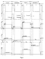
- the selection switch T4 and the clamping switch T3 are simultaneously closed by respectively applying to the electrodes Y S and Y C a suitable logic signal (see the first two chronograms of FIG. figure 3 ); the closing of T4 has the effect of selecting the control circuit 1 of the diode 2 by coupling, via the capacitor C C , the control terminal C to the address electrode X D ; the simultaneous closing of the switches T3 and T4 has the effect, despite the capacitive coupling, of setting the potential of the control terminal C to the setting potential V cal applied to the reference electrode P R ; during the setting of the control terminal C, the potential of the addressing electrode is raised to the value V ini-P-1 , the value of which will be determined later.
- the duration of this step is sufficiently high to obtain the stabilization of the potentials, and in particular so that the potential of the control terminal C remains at the value V cal .
- Step 5 addressing the circuit during the depolarization period :
- step 5 The duration of step 5 is adapted in a manner known per se to obtain the stabilization of the potentials at these values and to charge the holding capacitor C S.
- the modulator T2 begins to be depolarized in proportion to the value of V prog-pol-1 .
- Step 6 for maintaining the circuit during the depolarization period :
- the selection switch T4 is opened while keeping the clamping switch T3 open; the control circuit 1 is no longer selected and there is no longer any capacitive coupling between the addressing electrode X D and the control terminal C of the circuit 1.
- the capacitor C S a constant value the control voltage of the modulator T2, and the modulator T2 continues to be depolarized in proportion to the value of V prog-pol-1 .
- control voltage of the modulator T2 undergoes a slight drop - ⁇ V prog-pol-cor between step 4 and step 5 due to the suppression of the capacitive coupling; so that the depolarization of the modulator is in accordance with objectives, it is then preferable to make a correction + ⁇ V prog-pol-cor to the value V prog-pol-1 referred to in step 4.
- steps 4 and 5 are applied to the control circuits of the other diode lines so as to depolarize the modulators of the circuits of the other lines; the depolarization of the modulators of the whole panel is thus obtained.
- the end of this step marks the end of the depolarization period of the modulator T2 and the beginning of a new transmission period of the diode 2, during a new image frame.
- the figure 3 represents the control timing diagrams of a control circuit 1 of a transmitter 2 for two successive image frames.
- V prog-pol-1 V data-1 , V ini-P-1 , V pol-1
- the potentials of the control terminal C successively take the values V cal , V prog-data-2 , V cal , V prog-pol-2
- ⁇ V data-2 V data-2 -V ini-E
- ⁇ V prog-data-2 V prog-data-2 - V cal
- ⁇ V pol-2 V pol-2 -V ini-P-2
- ⁇ V prog-pol-2 V prog-pol-2 -V cal .
- the duration of this step be at least equal to 5 ⁇ ⁇ . .
- the value of R4 is generally high, of the order of one hundred kiloOhms, which induces a relatively high time constant ⁇ .
- V prog-data-2 >> V prog-data-1 , which means that the modulator T2 is much more strongly polarized during the second frame than during the first frame, causing a variation of the trigger threshold voltage this much larger modulator; therefore, we choose
- FIG. figure 2 A variant of the first embodiment is illustrated in FIG. figure 2 : the display panel is identical to the previous except that the T3 stall switch is able to connect directly, without going through the selection switch T4, the clamping terminal R to the control terminal C of the circuit 1 '.
- the panel according to this variant can be controlled as described above for the main embodiment.
- the embodiments described below relate to display panels with organic electroluminescent diodes active matrix; the invention applies more generally to all kinds of active matrix display panels, including current-controllable emitters or optical valves.
Landscapes
- Engineering & Computer Science (AREA)
- Physics & Mathematics (AREA)
- Computer Hardware Design (AREA)
- General Physics & Mathematics (AREA)
- Theoretical Computer Science (AREA)
- Chemical & Material Sciences (AREA)
- Crystallography & Structural Chemistry (AREA)
- Control Of Indicators Other Than Cathode Ray Tubes (AREA)
- Electroluminescent Light Sources (AREA)
Claims (5)
- Verfahren zur Steuerung eines Anzeigebildschirms mit- einem Gitter aus Lichtsendern oder optischen Ventilen,- einer aktiven Matrix mit einem Gitter aus Elektroden für die Adressierung (XD) von Spannungssignalen, einem Gitter aus Auswahlelektroden (YS), einem Gitter aus Klemmelektroden (YC), mindestens einer Referenzelektrode für die Adressierung (PR), einem Gitter aus Schaltkreisen, die geeignet sind, jeden der Lichtsender bzw. Ventile zu steuern, und jeweils (1, 1') mit einem Spannungssteueranschluss (C), der geeignet ist, mit einer Adressierelektrode (XD) über einen Kopplungskondensator (CC) und einen Auswahlschalter (T4), die in Serie geschaltet sind, gekoppelt zu werden, mit einem Spannungseinstellanschluss (R), der geeignet ist, über einen Einstellschalter (T3) mit dem Steueranschluss (C) verbunden zu werden, und mit einem zwischen dem Steueranschluss (C) und dem Einstellanschluss (R) geschalteten Haltekondensator (CS) versehen sind,- wobei der Einstellanschluss (R) mit mindestens einer Referenzelektrode (PR) verbunden ist, wobei die Steuerung des Auswahlschalters (T4) mit einer Auswahlelektrode (YS) und die Steuerung des Einstellschalters (T3) mit einer Klemmelektrode (YC) verbunden sind,- wobei das Verfahren umfasst:dadurch gekennzeichnet, dass bei beliebiger Sende- bzw. Depolarisationsperiode und beliebiger angelegter vorbestimmter Sendespannung (Vprog-data) bzw. Depolarisationsspannung (Vprog-pol) die Signale (Vini-E, Vdata; Vini-P, Vpol), die an der Adressierelektrode (XD) angelegt sind, an die der Steueranschluss (C) gekoppelt werden kann, alle dieselbe Polarität aufweisen, und dass während der Sende- und Depolarisationsperioden die Spannung (VCAL), die an der Referenzelektrode (PR) angelegt ist, mit welcher der Einstellanschluss (R) verbunden ist, bei einem konstanten Wert gehalten wird.-- Sendeperioden, bei denen eine vorbestimmte Sendespannung (Vprog-data) mit einer ersten Polarität an dem Steueranschluss mindestens eines Schaltkreises des Anzeigebildschirms durch kapazitive Kopplung über den Kopplungskondensator (CC) angelegt wird infolge eines Spannungssprunges, der durch eine Aufeinanderfolge von Signalen (Vini-E, Vdata) erzeugt wird, welche an der Adressierelektrode angelegt werden, wobei die vorbestimmte Sendespannung (Vprog-data) anschließend an dem Steueranschluss mit Hilfe des Haltekondensators (CS) aufrechterhalten wird und-- Depolarisationsperioden, bei denen eine vorbestimmte Depolarisationsspannung (Vprog-pol) mit einer zweiten, zu der ersten Polarität umgekehrten Polarität an dem Steueranschluss mindestens eines Schaltkreises des Anzeigebildschirms durch kapazitive Kopplung über den Kopplungskondensator (CC) angelegt wird infolge eines Spannungssprunges, der durch eine Aufeinanderfolge von Signalen (Vini-P, Vpol) erzeugt wird, welche an der Adressierelektrode angelegt werden, wobei die vorbestimmte Depolarisationsspannung (Vprog-pol) anschließend an dem Steueranschluss mit Hilfe des Haltekondensators (CS) aufrechterhalten wird,
- Verfahren nach Anspruch 1, dadurch gekennzeichnet, dass die vorbestimmte Sendespannung (Vprog-data) oder Depolarisationsspannung (Vprog-pol) an dem Steueranschluss (C) des mindestens einen Schaltkreises (1, 1') durch kapazitive Kopplung gemäß den folgenden Schritten angelegt werden:- einem Schritt der Einstellung, bei dem bei Setzung der Referenzelektrode des Anzeigebildschirms (PR) auf ein Einstellpotenzial (Vcal) ein Auswahlsignal an der den Auswahlschalter (T4) steuernden Auswahlelektrode (YS) und ein Einstellsignal an der den Einstellschalter (T3) des Schaltkreises steuernden Klemmelektrode (YC) angelegt werden, wobei diese Signale geeignet sind, die Schalter (T4, T3) zu schließen, und während des gleichzeitigen Anlegens des Auswahlsignals und des Einstellsignals ein Spannungsanfangssignal (Vini-E, Vini-P) an der Adressierelektrode (XD) angelegt wird, an die der Steueranschluss (C) gekoppelt werden kann,- einem Schritt der Adressierung des Schaltkreises, bei dem nach Beendigung des Einstellsignals, jedoch bei Aufrechterhaltung des Auswahlsignals, nach erfolgter Einstellung des Potenzials des Steueranschlusses (C) auf das Einstellpotenzial (Vcal) des mit der Referenzelektrode (PR) verbundenen Einstellanschlusses (R) und nach dem Anlegen des Spannungsanfangssignals ein Spannungsendsignal (Vdata, Vpol) an der Adressierelektrode (XD) angelegt wird, wobei die Aufeinanderfolge des Spannungsanfangssignals (Vini-E, Vini-P) und des Spannungsendsignals an dieser Adressierelektrode (XD) den Spannungssprung (ΔVdata = Vdata - Vini-E, ΔVpol = Vpol - Vini-P) erzeugt, welcher wiederum einen Spannungssprung (ΔVprog-data = Vprog-data - Vcal, ΔVprog-pol = Vprog-pol - Vcal) an dem mit der Adressierelektrode (XD) gekoppelten Steueranschluss (C) erzeugt, wobei die Werte des Spannungsanfangssignals (Vini-E, Vini-P) und des Spannungsendsignals (Vdata, Vpol) geeignet sind, nach dem Spannungssprung an dem Steueranschluss (C) die vorbestimmte Spannung (Vprog-data, Vprog-pol) zu erzielen.
- Verfahren nach einem der vorhergehenden Ansprüche, dadurch gekennzeichnet, dass der Anzeigebildschirm ein Gitter aus Lichtsendern aufweist, die geeignet sind, zwischen mindestens einer Speisungsbasiselektrode PB und mindestens einer oberen Speisungselektrode PA gespeist zu werden, wobei jeder der einen Lichtsender (2) steuernden Schaltkreise einen Strommodulator (T2) mit einer die Steuerelektrode (C) des Schaltkreises bildenden Spannungssteuerelektrode (G) und zwei zwischen einer der Speisungselektroden (PA, PB) und einer Speisungselektrode des Lichtsenders geschalteten Stromdurchgangselektroden (D, S) umfasst.
- Verfahren nach Anspruch 3, dadurch gekennzeichnet, dass es sich bei dem Strommodulator um einen Transistor mit einer Halbleiterschicht aus amorphem Silicium handelt.
- Verfahren nach Anspruch 3 oder 4, dadurch gekennzeichnet, dass es sich bei den Lichtsendern um LEDs handelt.
Applications Claiming Priority (2)
| Application Number | Priority Date | Filing Date | Title |
|---|---|---|---|
| FR0553978A FR2895130A1 (fr) | 2005-12-20 | 2005-12-20 | Procede de pilotage d'un panneau d'affichage par couplage capacitif |
| PCT/EP2006/069924 WO2007071680A1 (fr) | 2005-12-20 | 2006-12-19 | Procede de pilotage d'un panneau d'affichage par couplage capacitif |
Publications (2)
| Publication Number | Publication Date |
|---|---|
| EP1964094A1 EP1964094A1 (de) | 2008-09-03 |
| EP1964094B1 true EP1964094B1 (de) | 2010-04-14 |
Family
ID=36123182
Family Applications (1)
| Application Number | Title | Priority Date | Filing Date |
|---|---|---|---|
| EP06841466A Ceased EP1964094B1 (de) | 2005-12-20 | 2006-12-19 | Verfahren zur steuerung eines anzeigeschirms durch kapazitive kopplung |
Country Status (8)
| Country | Link |
|---|---|
| US (1) | US8362984B2 (de) |
| EP (1) | EP1964094B1 (de) |
| JP (1) | JP5666778B2 (de) |
| KR (1) | KR101399464B1 (de) |
| DE (1) | DE602006013704D1 (de) |
| FR (1) | FR2895130A1 (de) |
| TW (1) | TWI409742B (de) |
| WO (1) | WO2007071680A1 (de) |
Cited By (1)
| Publication number | Priority date | Publication date | Assignee | Title |
|---|---|---|---|---|
| US11322082B2 (en) | 2017-09-15 | 2022-05-03 | Chongqing Boe Optoelectronics Technology Co., Ltd. | Pixel driving circuit including compensation elements and method and display device |
Families Citing this family (5)
| Publication number | Priority date | Publication date | Assignee | Title |
|---|---|---|---|---|
| FR2895131A1 (fr) * | 2005-12-20 | 2007-06-22 | Thomson Licensing Sas | Panneau d'affichage et procede de pilotage avec couplage capacitif transitoire |
| JP5186950B2 (ja) * | 2008-02-28 | 2013-04-24 | ソニー株式会社 | El表示パネル、電子機器及びel表示パネルの駆動方法 |
| US20090290773A1 (en) * | 2008-05-21 | 2009-11-26 | Varian Medical Systems, Inc. | Apparatus and Method to Facilitate User-Modified Rendering of an Object Image |
| KR101658037B1 (ko) * | 2010-11-09 | 2016-09-21 | 삼성전자주식회사 | 능동형 디스플레이 장치의 구동 방법 |
| KR102093664B1 (ko) * | 2012-11-20 | 2020-04-16 | 삼성디스플레이 주식회사 | 표시 장치 및 그 구동 방법 |
Citations (1)
| Publication number | Priority date | Publication date | Assignee | Title |
|---|---|---|---|---|
| EP1517290A2 (de) * | 2003-08-29 | 2005-03-23 | Seiko Epson Corporation | Treiber für elektrolumineszente Bildanzeigevorrichtung und Steuerverfahren dafür |
Family Cites Families (24)
| Publication number | Priority date | Publication date | Assignee | Title |
|---|---|---|---|---|
| US5005A (en) * | 1847-03-06 | Iien ry | ||
| US1002A (en) * | 1838-11-09 | Joseph evens | ||
| US6229506B1 (en) * | 1997-04-23 | 2001-05-08 | Sarnoff Corporation | Active matrix light emitting diode pixel structure and concomitant method |
| JP3767877B2 (ja) * | 1997-09-29 | 2006-04-19 | 三菱化学株式会社 | アクティブマトリックス発光ダイオード画素構造およびその方法 |
| JP2001117534A (ja) | 1999-10-21 | 2001-04-27 | Pioneer Electronic Corp | アクティブマトリクス型表示装置及びその駆動方法 |
| US6864863B2 (en) | 2000-10-12 | 2005-03-08 | Seiko Epson Corporation | Driving circuit including organic electroluminescent element, electronic equipment, and electro-optical device |
| JPWO2002075709A1 (ja) * | 2001-03-21 | 2004-07-08 | キヤノン株式会社 | アクティブマトリクス型発光素子の駆動回路 |
| US6985141B2 (en) * | 2001-07-10 | 2006-01-10 | Canon Kabushiki Kaisha | Display driving method and display apparatus utilizing the same |
| US6858989B2 (en) * | 2001-09-20 | 2005-02-22 | Emagin Corporation | Method and system for stabilizing thin film transistors in AMOLED displays |
| JP2003186437A (ja) * | 2001-12-18 | 2003-07-04 | Sanyo Electric Co Ltd | 表示装置 |
| GB0130411D0 (en) * | 2001-12-20 | 2002-02-06 | Koninkl Philips Electronics Nv | Active matrix electroluminescent display device |
| JP4146129B2 (ja) * | 2002-01-22 | 2008-09-03 | パイオニア株式会社 | プラズマディスプレイパネルの駆動方法及び駆動装置 |
| JP4123084B2 (ja) * | 2002-07-31 | 2008-07-23 | セイコーエプソン株式会社 | 電子回路、電気光学装置、及び電子機器 |
| JP3949040B2 (ja) * | 2002-09-25 | 2007-07-25 | 東北パイオニア株式会社 | 発光表示パネルの駆動装置 |
| JP2004157467A (ja) * | 2002-11-08 | 2004-06-03 | Tohoku Pioneer Corp | アクティブ型発光表示パネルの駆動方法および駆動装置 |
| EP1627372A1 (de) * | 2003-05-02 | 2006-02-22 | Koninklijke Philips Electronics N.V. | Oled anzeige mit aktiver matrix mit driftkompensation der schwellenspannung |
| TWI261213B (en) * | 2003-08-21 | 2006-09-01 | Seiko Epson Corp | Optoelectronic apparatus and electronic machine |
| JP4608999B2 (ja) | 2003-08-29 | 2011-01-12 | セイコーエプソン株式会社 | 電子回路の駆動方法、電子回路、電子装置、電気光学装置、電子機器および電子装置の駆動方法 |
| KR100514183B1 (ko) * | 2003-09-08 | 2005-09-13 | 삼성에스디아이 주식회사 | 유기 전계발광 표시장치의 픽셀구동회로 및 그 구동방법 |
| JP4907356B2 (ja) | 2003-12-23 | 2012-03-28 | トムソン ライセンシング | 表示装置 |
| KR100965597B1 (ko) * | 2003-12-29 | 2010-06-23 | 엘지디스플레이 주식회사 | 액정표시장치의 구동방법 및 구동장치 |
| EP1700290B1 (de) | 2003-12-31 | 2019-01-16 | Thomson Licensing | Bildanzeigeschirm und verfahren zur adressierung des schirms |
| FR2895131A1 (fr) * | 2005-12-20 | 2007-06-22 | Thomson Licensing Sas | Panneau d'affichage et procede de pilotage avec couplage capacitif transitoire |
| TWI419105B (zh) * | 2005-12-20 | 2013-12-11 | 湯姆生特許公司 | 顯示面板之驅動方法 |
-
2005
- 2005-12-20 FR FR0553978A patent/FR2895130A1/fr active Pending
-
2006
- 2006-12-15 TW TW095146973A patent/TWI409742B/zh not_active IP Right Cessation
- 2006-12-19 DE DE602006013704T patent/DE602006013704D1/de active Active
- 2006-12-19 EP EP06841466A patent/EP1964094B1/de not_active Ceased
- 2006-12-19 JP JP2008546428A patent/JP5666778B2/ja not_active Expired - Fee Related
- 2006-12-19 WO PCT/EP2006/069924 patent/WO2007071680A1/fr not_active Ceased
- 2006-12-19 KR KR1020087014843A patent/KR101399464B1/ko not_active Expired - Fee Related
- 2006-12-19 US US12/086,731 patent/US8362984B2/en not_active Expired - Fee Related
Patent Citations (1)
| Publication number | Priority date | Publication date | Assignee | Title |
|---|---|---|---|---|
| EP1517290A2 (de) * | 2003-08-29 | 2005-03-23 | Seiko Epson Corporation | Treiber für elektrolumineszente Bildanzeigevorrichtung und Steuerverfahren dafür |
Cited By (1)
| Publication number | Priority date | Publication date | Assignee | Title |
|---|---|---|---|---|
| US11322082B2 (en) | 2017-09-15 | 2022-05-03 | Chongqing Boe Optoelectronics Technology Co., Ltd. | Pixel driving circuit including compensation elements and method and display device |
Also Published As
| Publication number | Publication date |
|---|---|
| TW200735016A (en) | 2007-09-16 |
| KR101399464B1 (ko) | 2014-05-26 |
| WO2007071680A1 (fr) | 2007-06-28 |
| DE602006013704D1 (de) | 2010-05-27 |
| EP1964094A1 (de) | 2008-09-03 |
| KR20080080559A (ko) | 2008-09-04 |
| FR2895130A1 (fr) | 2007-06-22 |
| TWI409742B (zh) | 2013-09-21 |
| US8362984B2 (en) | 2013-01-29 |
| US20090015575A1 (en) | 2009-01-15 |
| JP5666778B2 (ja) | 2015-02-12 |
| JP2009520226A (ja) | 2009-05-21 |
Similar Documents
| Publication | Publication Date | Title |
|---|---|---|
| EP2033178B1 (de) | Vorrichtung zur aktivmatrix-anzeigekompensation | |
| WO2007125095A1 (fr) | Ecran electroluminescent organique | |
| FR2884639A1 (fr) | Panneau d'affichage d'images a matrice active, dont les emetteurs sont alimentes par des generateurs de courant pilotables en tension | |
| JP2004280059A (ja) | 表示装置 | |
| EP3079142B1 (de) | Bildanzeigeverfahren auf matrix-bildschirm | |
| EP1964093B1 (de) | Antriebsverfahren für eine plasmaanzeigetafel mit depolarisierung | |
| EP1851747B1 (de) | Pixeladressierungsschaltung und verfahren zur steuerung solcher schaltung | |
| EP1964095B1 (de) | Anzeigeschirm und steuerverfarhen mit transienter kapazitiver kopplung | |
| EP1700290B1 (de) | Bildanzeigeschirm und verfahren zur adressierung des schirms | |
| EP1964094A1 (de) | Verfahren zur steuerung eines anzeigeschirms durch kapazitive kopplung | |
| WO2015028448A1 (fr) | Ecran a matrice active a regulation de tensions d'alimentation en fonction de la temperature | |
| EP1697920B1 (de) | Vorrichtung zum anzeigen von bildern auf einer oled aktivmatrix | |
| EP1958182B1 (de) | Videosystem mit einer durch ein verbessertes adressierungsverfahren gesteuerten flussigkristallmatrixanzeige | |
| EP1771838B1 (de) | Bildanzeigevorrichtung und steuerungsverfahren für die anzeigevorrichtung | |
| EP1864275B1 (de) | Bildanzeigeeinrichtung und verfahren zu ihrer steuerung | |
| EP1958183B1 (de) | Sequentielle farbbeleuchtungs-flüssigkristall-matrixanzeige | |
| JP2006251201A (ja) | 発光表示装置 | |
| FR2846794A1 (fr) | Panneau organique electroluminescent bi-stable ou chaque cellule comprend une diode de shockley | |
| FR2869143A1 (fr) | Panneau electroluminescent bistable a trois reseaux d'electrodes | |
| FR2843225A1 (fr) | Dispositif de visualisation d'images a matrice active et a compensation de seuil de declenchement | |
| FR2886497A1 (fr) | Dispositif d'affichage d'images video a matrice active avec correction des non-uniformites de luminance |
Legal Events
| Date | Code | Title | Description |
|---|---|---|---|
| PUAI | Public reference made under article 153(3) epc to a published international application that has entered the european phase |
Free format text: ORIGINAL CODE: 0009012 |
|
| 17P | Request for examination filed |
Effective date: 20080616 |
|
| AK | Designated contracting states |
Kind code of ref document: A1 Designated state(s): DE FR GB |
|
| DAX | Request for extension of the european patent (deleted) | ||
| RBV | Designated contracting states (corrected) |
Designated state(s): DE FR GB |
|
| GRAP | Despatch of communication of intention to grant a patent |
Free format text: ORIGINAL CODE: EPIDOSNIGR1 |
|
| RAP1 | Party data changed (applicant data changed or rights of an application transferred) |
Owner name: THOMSON LICENSING |
|
| GRAS | Grant fee paid |
Free format text: ORIGINAL CODE: EPIDOSNIGR3 |
|
| GRAA | (expected) grant |
Free format text: ORIGINAL CODE: 0009210 |
|
| AK | Designated contracting states |
Kind code of ref document: B1 Designated state(s): DE FR GB |
|
| REG | Reference to a national code |
Ref country code: GB Ref legal event code: FG4D Free format text: NOT ENGLISH |
|
| REF | Corresponds to: |
Ref document number: 602006013704 Country of ref document: DE Date of ref document: 20100527 Kind code of ref document: P |
|
| PLBE | No opposition filed within time limit |
Free format text: ORIGINAL CODE: 0009261 |
|
| STAA | Information on the status of an ep patent application or granted ep patent |
Free format text: STATUS: NO OPPOSITION FILED WITHIN TIME LIMIT |
|
| 26N | No opposition filed |
Effective date: 20110117 |
|
| REG | Reference to a national code |
Ref country code: FR Ref legal event code: PLFP Year of fee payment: 10 |
|
| REG | Reference to a national code |
Ref country code: FR Ref legal event code: PLFP Year of fee payment: 11 |
|
| REG | Reference to a national code |
Ref country code: DE Ref legal event code: R082 Ref document number: 602006013704 Country of ref document: DE Representative=s name: HOFSTETTER, SCHURACK & PARTNER PATENT- UND REC, DE |
|
| REG | Reference to a national code |
Ref country code: FR Ref legal event code: PLFP Year of fee payment: 12 |
|
| PGFP | Annual fee paid to national office [announced via postgrant information from national office to epo] |
Ref country code: FR Payment date: 20181231 Year of fee payment: 13 Ref country code: GB Payment date: 20181218 Year of fee payment: 13 |
|
| PGFP | Annual fee paid to national office [announced via postgrant information from national office to epo] |
Ref country code: DE Payment date: 20181211 Year of fee payment: 13 |
|
| REG | Reference to a national code |
Ref country code: DE Ref legal event code: R119 Ref document number: 602006013704 Country of ref document: DE |
|
| GBPC | Gb: european patent ceased through non-payment of renewal fee |
Effective date: 20191219 |
|
| PG25 | Lapsed in a contracting state [announced via postgrant information from national office to epo] |
Ref country code: GB Free format text: LAPSE BECAUSE OF NON-PAYMENT OF DUE FEES Effective date: 20191219 Ref country code: DE Free format text: LAPSE BECAUSE OF NON-PAYMENT OF DUE FEES Effective date: 20200701 Ref country code: FR Free format text: LAPSE BECAUSE OF NON-PAYMENT OF DUE FEES Effective date: 20191231 |