EP1864275B1 - Bildanzeigeeinrichtung und verfahren zu ihrer steuerung - Google Patents
Bildanzeigeeinrichtung und verfahren zu ihrer steuerung Download PDFInfo
- Publication number
- EP1864275B1 EP1864275B1 EP06709267A EP06709267A EP1864275B1 EP 1864275 B1 EP1864275 B1 EP 1864275B1 EP 06709267 A EP06709267 A EP 06709267A EP 06709267 A EP06709267 A EP 06709267A EP 1864275 B1 EP1864275 B1 EP 1864275B1
- Authority
- EP
- European Patent Office
- Prior art keywords
- emitters
- selection
- voltage
- electrode
- modulator
- Prior art date
- Legal status (The legal status is an assumption and is not a legal conclusion. Google has not performed a legal analysis and makes no representation as to the accuracy of the status listed.)
- Active
Links
- 238000000034 method Methods 0.000 title claims description 11
- 239000003990 capacitor Substances 0.000 claims description 46
- 239000011159 matrix material Substances 0.000 claims description 3
- 230000010287 polarization Effects 0.000 description 7
- 229910021417 amorphous silicon Inorganic materials 0.000 description 5
- 239000010409 thin film Substances 0.000 description 5
- 230000005540 biological transmission Effects 0.000 description 3
- 238000005516 engineering process Methods 0.000 description 3
- 229910021420 polycrystalline silicon Inorganic materials 0.000 description 3
- 230000002123 temporal effect Effects 0.000 description 3
- 206010052143 Ocular discomfort Diseases 0.000 description 2
- XUIMIQQOPSSXEZ-UHFFFAOYSA-N Silicon Chemical compound [Si] XUIMIQQOPSSXEZ-UHFFFAOYSA-N 0.000 description 1
- 238000002425 crystallisation Methods 0.000 description 1
- 230000008025 crystallization Effects 0.000 description 1
- 230000007423 decrease Effects 0.000 description 1
- 239000011521 glass Substances 0.000 description 1
- 238000005286 illumination Methods 0.000 description 1
- 238000004519 manufacturing process Methods 0.000 description 1
- 238000011017 operating method Methods 0.000 description 1
- 230000000750 progressive effect Effects 0.000 description 1
- 230000008929 regeneration Effects 0.000 description 1
- 238000011069 regeneration method Methods 0.000 description 1
- 230000011664 signaling Effects 0.000 description 1
- 229910052710 silicon Inorganic materials 0.000 description 1
- 239000010703 silicon Substances 0.000 description 1
- 239000000758 substrate Substances 0.000 description 1
Images


Classifications
-
- G—PHYSICS
- G09—EDUCATION; CRYPTOGRAPHY; DISPLAY; ADVERTISING; SEALS
- G09G—ARRANGEMENTS OR CIRCUITS FOR CONTROL OF INDICATING DEVICES USING STATIC MEANS TO PRESENT VARIABLE INFORMATION
- G09G3/00—Control arrangements or circuits, of interest only in connection with visual indicators other than cathode-ray tubes
- G09G3/20—Control arrangements or circuits, of interest only in connection with visual indicators other than cathode-ray tubes for presentation of an assembly of a number of characters, e.g. a page, by composing the assembly by combination of individual elements arranged in a matrix no fixed position being assigned to or needed to be assigned to the individual characters or partial characters
- G09G3/22—Control arrangements or circuits, of interest only in connection with visual indicators other than cathode-ray tubes for presentation of an assembly of a number of characters, e.g. a page, by composing the assembly by combination of individual elements arranged in a matrix no fixed position being assigned to or needed to be assigned to the individual characters or partial characters using controlled light sources
- G09G3/30—Control arrangements or circuits, of interest only in connection with visual indicators other than cathode-ray tubes for presentation of an assembly of a number of characters, e.g. a page, by composing the assembly by combination of individual elements arranged in a matrix no fixed position being assigned to or needed to be assigned to the individual characters or partial characters using controlled light sources using electroluminescent panels
- G09G3/32—Control arrangements or circuits, of interest only in connection with visual indicators other than cathode-ray tubes for presentation of an assembly of a number of characters, e.g. a page, by composing the assembly by combination of individual elements arranged in a matrix no fixed position being assigned to or needed to be assigned to the individual characters or partial characters using controlled light sources using electroluminescent panels semiconductive, e.g. using light-emitting diodes [LED]
- G09G3/3208—Control arrangements or circuits, of interest only in connection with visual indicators other than cathode-ray tubes for presentation of an assembly of a number of characters, e.g. a page, by composing the assembly by combination of individual elements arranged in a matrix no fixed position being assigned to or needed to be assigned to the individual characters or partial characters using controlled light sources using electroluminescent panels semiconductive, e.g. using light-emitting diodes [LED] organic, e.g. using organic light-emitting diodes [OLED]
- G09G3/3225—Control arrangements or circuits, of interest only in connection with visual indicators other than cathode-ray tubes for presentation of an assembly of a number of characters, e.g. a page, by composing the assembly by combination of individual elements arranged in a matrix no fixed position being assigned to or needed to be assigned to the individual characters or partial characters using controlled light sources using electroluminescent panels semiconductive, e.g. using light-emitting diodes [LED] organic, e.g. using organic light-emitting diodes [OLED] using an active matrix
- G09G3/3233—Control arrangements or circuits, of interest only in connection with visual indicators other than cathode-ray tubes for presentation of an assembly of a number of characters, e.g. a page, by composing the assembly by combination of individual elements arranged in a matrix no fixed position being assigned to or needed to be assigned to the individual characters or partial characters using controlled light sources using electroluminescent panels semiconductive, e.g. using light-emitting diodes [LED] organic, e.g. using organic light-emitting diodes [OLED] using an active matrix with pixel circuitry controlling the current through the light-emitting element
-
- G—PHYSICS
- G09—EDUCATION; CRYPTOGRAPHY; DISPLAY; ADVERTISING; SEALS
- G09G—ARRANGEMENTS OR CIRCUITS FOR CONTROL OF INDICATING DEVICES USING STATIC MEANS TO PRESENT VARIABLE INFORMATION
- G09G3/00—Control arrangements or circuits, of interest only in connection with visual indicators other than cathode-ray tubes
- G09G3/20—Control arrangements or circuits, of interest only in connection with visual indicators other than cathode-ray tubes for presentation of an assembly of a number of characters, e.g. a page, by composing the assembly by combination of individual elements arranged in a matrix no fixed position being assigned to or needed to be assigned to the individual characters or partial characters
- G09G3/22—Control arrangements or circuits, of interest only in connection with visual indicators other than cathode-ray tubes for presentation of an assembly of a number of characters, e.g. a page, by composing the assembly by combination of individual elements arranged in a matrix no fixed position being assigned to or needed to be assigned to the individual characters or partial characters using controlled light sources
- G09G3/30—Control arrangements or circuits, of interest only in connection with visual indicators other than cathode-ray tubes for presentation of an assembly of a number of characters, e.g. a page, by composing the assembly by combination of individual elements arranged in a matrix no fixed position being assigned to or needed to be assigned to the individual characters or partial characters using controlled light sources using electroluminescent panels
-
- G—PHYSICS
- G09—EDUCATION; CRYPTOGRAPHY; DISPLAY; ADVERTISING; SEALS
- G09G—ARRANGEMENTS OR CIRCUITS FOR CONTROL OF INDICATING DEVICES USING STATIC MEANS TO PRESENT VARIABLE INFORMATION
- G09G3/00—Control arrangements or circuits, of interest only in connection with visual indicators other than cathode-ray tubes
- G09G3/20—Control arrangements or circuits, of interest only in connection with visual indicators other than cathode-ray tubes for presentation of an assembly of a number of characters, e.g. a page, by composing the assembly by combination of individual elements arranged in a matrix no fixed position being assigned to or needed to be assigned to the individual characters or partial characters
- G09G3/22—Control arrangements or circuits, of interest only in connection with visual indicators other than cathode-ray tubes for presentation of an assembly of a number of characters, e.g. a page, by composing the assembly by combination of individual elements arranged in a matrix no fixed position being assigned to or needed to be assigned to the individual characters or partial characters using controlled light sources
- G09G3/30—Control arrangements or circuits, of interest only in connection with visual indicators other than cathode-ray tubes for presentation of an assembly of a number of characters, e.g. a page, by composing the assembly by combination of individual elements arranged in a matrix no fixed position being assigned to or needed to be assigned to the individual characters or partial characters using controlled light sources using electroluminescent panels
- G09G3/32—Control arrangements or circuits, of interest only in connection with visual indicators other than cathode-ray tubes for presentation of an assembly of a number of characters, e.g. a page, by composing the assembly by combination of individual elements arranged in a matrix no fixed position being assigned to or needed to be assigned to the individual characters or partial characters using controlled light sources using electroluminescent panels semiconductive, e.g. using light-emitting diodes [LED]
- G09G3/3208—Control arrangements or circuits, of interest only in connection with visual indicators other than cathode-ray tubes for presentation of an assembly of a number of characters, e.g. a page, by composing the assembly by combination of individual elements arranged in a matrix no fixed position being assigned to or needed to be assigned to the individual characters or partial characters using controlled light sources using electroluminescent panels semiconductive, e.g. using light-emitting diodes [LED] organic, e.g. using organic light-emitting diodes [OLED]
- G09G3/3225—Control arrangements or circuits, of interest only in connection with visual indicators other than cathode-ray tubes for presentation of an assembly of a number of characters, e.g. a page, by composing the assembly by combination of individual elements arranged in a matrix no fixed position being assigned to or needed to be assigned to the individual characters or partial characters using controlled light sources using electroluminescent panels semiconductive, e.g. using light-emitting diodes [LED] organic, e.g. using organic light-emitting diodes [OLED] using an active matrix
- G09G3/3258—Control arrangements or circuits, of interest only in connection with visual indicators other than cathode-ray tubes for presentation of an assembly of a number of characters, e.g. a page, by composing the assembly by combination of individual elements arranged in a matrix no fixed position being assigned to or needed to be assigned to the individual characters or partial characters using controlled light sources using electroluminescent panels semiconductive, e.g. using light-emitting diodes [LED] organic, e.g. using organic light-emitting diodes [OLED] using an active matrix with pixel circuitry controlling the voltage across the light-emitting element
-
- H—ELECTRICITY
- H05—ELECTRIC TECHNIQUES NOT OTHERWISE PROVIDED FOR
- H05B—ELECTRIC HEATING; ELECTRIC LIGHT SOURCES NOT OTHERWISE PROVIDED FOR; CIRCUIT ARRANGEMENTS FOR ELECTRIC LIGHT SOURCES, IN GENERAL
- H05B33/00—Electroluminescent light sources
- H05B33/12—Light sources with substantially two-dimensional radiating surfaces
-
- G—PHYSICS
- G09—EDUCATION; CRYPTOGRAPHY; DISPLAY; ADVERTISING; SEALS
- G09G—ARRANGEMENTS OR CIRCUITS FOR CONTROL OF INDICATING DEVICES USING STATIC MEANS TO PRESENT VARIABLE INFORMATION
- G09G2300/00—Aspects of the constitution of display devices
- G09G2300/04—Structural and physical details of display devices
- G09G2300/0404—Matrix technologies
- G09G2300/0417—Special arrangements specific to the use of low carrier mobility technology
-
- G—PHYSICS
- G09—EDUCATION; CRYPTOGRAPHY; DISPLAY; ADVERTISING; SEALS
- G09G—ARRANGEMENTS OR CIRCUITS FOR CONTROL OF INDICATING DEVICES USING STATIC MEANS TO PRESENT VARIABLE INFORMATION
- G09G2300/00—Aspects of the constitution of display devices
- G09G2300/08—Active matrix structure, i.e. with use of active elements, inclusive of non-linear two terminal elements, in the pixels together with light emitting or modulating elements
- G09G2300/0809—Several active elements per pixel in active matrix panels
- G09G2300/0842—Several active elements per pixel in active matrix panels forming a memory circuit, e.g. a dynamic memory with one capacitor
-
- G—PHYSICS
- G09—EDUCATION; CRYPTOGRAPHY; DISPLAY; ADVERTISING; SEALS
- G09G—ARRANGEMENTS OR CIRCUITS FOR CONTROL OF INDICATING DEVICES USING STATIC MEANS TO PRESENT VARIABLE INFORMATION
- G09G2300/00—Aspects of the constitution of display devices
- G09G2300/08—Active matrix structure, i.e. with use of active elements, inclusive of non-linear two terminal elements, in the pixels together with light emitting or modulating elements
- G09G2300/0876—Supplementary capacities in pixels having special driving circuits and electrodes instead of being connected to common electrode or ground; Use of additional capacitively coupled compensation electrodes
-
- G—PHYSICS
- G09—EDUCATION; CRYPTOGRAPHY; DISPLAY; ADVERTISING; SEALS
- G09G—ARRANGEMENTS OR CIRCUITS FOR CONTROL OF INDICATING DEVICES USING STATIC MEANS TO PRESENT VARIABLE INFORMATION
- G09G2310/00—Command of the display device
- G09G2310/02—Addressing, scanning or driving the display screen or processing steps related thereto
- G09G2310/0243—Details of the generation of driving signals
- G09G2310/0251—Precharge or discharge of pixel before applying new pixel voltage
-
- G—PHYSICS
- G09—EDUCATION; CRYPTOGRAPHY; DISPLAY; ADVERTISING; SEALS
- G09G—ARRANGEMENTS OR CIRCUITS FOR CONTROL OF INDICATING DEVICES USING STATIC MEANS TO PRESENT VARIABLE INFORMATION
- G09G2310/00—Command of the display device
- G09G2310/02—Addressing, scanning or driving the display screen or processing steps related thereto
- G09G2310/0243—Details of the generation of driving signals
- G09G2310/0254—Control of polarity reversal in general, other than for liquid crystal displays
-
- G—PHYSICS
- G09—EDUCATION; CRYPTOGRAPHY; DISPLAY; ADVERTISING; SEALS
- G09G—ARRANGEMENTS OR CIRCUITS FOR CONTROL OF INDICATING DEVICES USING STATIC MEANS TO PRESENT VARIABLE INFORMATION
- G09G2320/00—Control of display operating conditions
- G09G2320/04—Maintaining the quality of display appearance
- G09G2320/043—Preventing or counteracting the effects of ageing
Definitions
- An OLED (Organic Light Emitting Diode) active matrix display device comprises light emitters formed from organic electroluminescent cells.
- such a device For the control of these emitters, such a device comprises thin film transistors, called TFT (Thin Film Transistor) transistors. These transistors are able to control the current flowing through the emitters. They are made of polycrystalline silicon, for example using low temperature amorphous silicon (LTPS) crystallization technology, or directly in amorphous silicon.
- TFT Thin Film Transistor
- the TFT manufacturing technology introduces local spatial variations in the trigger threshold voltage of these transistors.
- TFT transistors fed by the same supply voltage and controlled by identical voltages generate currents of different intensities which result in a non-uniform brightness of the display device comprising such transistors.
- spatial variations in the luminance of the pixels of the display device and a visible visual discomfort for the user.
- the instability of the amorphous silicon results in a variation of the characteristics of the TFT when a voltage is applied between the gate and the source of the TFT. More particularly, the triggering threshold voltage of the TFT transistors increases when a positive polarity voltage is applied. is applied their gate and their source and decreases when a negative polarity voltage is applied between their gate and their source. Since the voltage applied between the gate and the source of the transistors generally differs from one transistor to the other according to the luminance deviations of the pixels of an image to be displayed, the degree of fluctuation of the trigger threshold voltage differs from one transistor to another. As a result, the resulting luminance variation is unevenly distributed on the display device, resulting in changes over time in the luminance of the display pixels and obvious visual discomfort for the display. 'user.
- the document US 2003/0052614 discloses an image display device of the aforementioned type.
- This device comprises in particular, for each transmitter column, a control switch controlled by an electrode control to move this switch between a connection position to a reverse bias generator and a connection position to a column driving unit.
- the inverse polarization generator is able to apply between the gate and the source of the modulators associated with the emitters of a column, a reverse bias voltage during so-called modulator regeneration phases, adapted to compensate for the drifts of their threshold voltage. trigger.
- This reverse bias voltage has a polarity inverse to the polarity of the addressing voltages applied between the gate and the source of these same modulators during illumination phases of the transmitters.
- the device described in the document US2003 / 0112205 does not allow to apply a reverse bias voltage between the gate and the source of the modulators associated with the transmitters of the same line: indeed, in this document, when a reverse bias is applied (see paragraph 44), is at the terminals of the transmitters (see for example the last sentence of paragraph 44) and not between the gate and the source of the modulators; indeed, during the phases of inverse polarization in question here, the gate and the source of the modulators are brought to the same potential by the simultaneous closing of the referenced switches Tr3 and Tr4, and there is no polarization, inverse or no, between the gate and the source.
- An object of the invention is in particular to provide an alternative display device adapted to compensate for the variations over time of the trigger threshold voltages.
- this device divides by two the number of line electrodes contained in the device.
- the emitters 2, 4, 6, 8 are organic light emitting diodes. They include an anode and a cathode. They emit a luminous intensity directly proportional to the current passing through them. Each transmitter constitutes an elementary pixel of the display device.
- the display device further comprises addressing circuits 18, 20, 22, 24 distributed along a network.
- Each addressing circuit is connected to a transmitter 2, 4, 6, 8 to drive it.
- Addressing circuits 18, 22; 20, 24 of each column of emitters 14, 16 are addressed via an addressing electrode 26, 28 of this column of emitters.
- Each addressing electrode 26, 28 is connected to a column driver unit 30 (in English: column driver).
- the control unit 30 is able to receive an image display signal and to transmit simultaneously to each addressing electrode 26, 28 of a column, an address voltage V data representative of a data item. display of a transmitter to be addressed in this column.
- Addressing circuits 18, 20; 22, 24 of each emitter line 10, 12 are selected via a selection electrode 32, 34, each connected to a selection control unit 33, 35.
- the selection control unit 33, 35 of a line of transmitters 10, 12 is adapted to generate at a preset frequency, a selection signal V 32 , V 34 at the selection electrode 32, 34 of this line 10, 12 to select all transmitters 2, 4 and 6, 8 of this line 10, 12.
- This selection signal comprises a series of pulses each generated at each new image frame. These pulses are logical data for selecting a transmitter of a line of transmitters.
- This circuit 18 comprises a current modulator 36, a selection switch 38, a storage capacitor 40 (referenced 41 in the addressing circuit 28 of the second emitter line 12) and two power supply electrodes 42, 44.
- the current modulator 36 and the switch 38 are thin film transistors (in English: Thin Film Transistor), based on a technology using polycrystalline silicon (Poly-Si), amorphous silicon (a-Si) or silicon microcrystalline (micro-Si) deposited in thin layers on a glass substrate.
- Such components comprise three electrodes: a drain electrode and a source electrode between which circulates a modulated current called drain current, and a gate electrode.
- the modulator 36 shown on the Fig.1 is of type N, so that, in operation, its drain current flows from its drain to its source. It will be noted that the device according to the invention can also be used to drive P-type TFT transistors.
- the capacitor 40 is able to store electrical charges to maintain a voltage at the gate of the modulator 36 after the transmission of an addressing voltage.
- the capacitor 40 comprises a first terminal 40a connected to the gate of the modulator 36 and a second terminal 40b connected to a reverse bias electrode 52.
- the display device 1 further comprises, for each line of emitters 10, 12, a reverse bias generator 46, 48 connected to a reverse bias electrode 52, 54 and a reverse bias control generator 53, 55 connected to a reverse bias control electrode 56, 58.
- the inverse polarization generators 46 and 48 are able to generate, each between the gate and the source of the modulators 36, a bias voltage V p of values possibly different from each other and of polarity opposite to the polarity of the addressing voltages V. data applied between the gate and the source of the modulators 36 during the transmission phases of the transmitters 2, 4, 6, 8.
- the reverse bias control generators 53, 55 are adapted to produce a reverse bias control signal V 56 , V 58 , similar to the selection signal V 32 , V 34 , of the same frequency and shifted by half a period or variable period with respect to this selection signal.
- the device 1 further comprises a reverse bias switch 59 in each addressing circuit 18, 20, 22, 24.
- a current-passing electrode (source or drain) of the switch 59 of each addressing circuit of an emitter line 10, 12 is connected to the inverse bias electrode 52, 54 of this emitter line. 10, 12, and therefore also to the second terminal 40b of the capacitor 40, 41.
- the other current-passing electrode (source or drain) of the switch 59 is connected to the gate of the modulator 36, and consequently, also at the first terminal 40a of the capacitor 40, 41.
- the gate of the switch 59 of each addressing circuit of an emitter line 10, 12 is connected to the reverse bias control electrode 56, 58 of this same emitter line 10, 12.
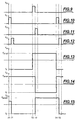
- a pulse of the selection signal V 32 represented on the Fig.2 is generated at the selection electrode 32 of the first line of transmitters 10.
- the control unit 30 addresses an address voltage V data2 to the addressing electrode 26.
- the value of this voltage d The addressing is referenced to the constant potential of the supply electrode 44.
- the switches 38 of the first line of emitters 10 close and the voltage V data2 is applied to the first terminal 40a of the capacitor 40 and between the gate and the source of the modulator 36 of the addressing circuit 18, as visible on the Fig.6 .
- the switches 38 of the first line of emitters 10 open and the voltage V data2 is maintained, thanks to the capacitor 40, between the gate and the source of the modulator 36 of the addressing circuit 18, as visible on the Fig.6 .
- a pulse of the selection signal V 34 represented on the Fig.4 is applied to the selection electrode 34.
- the control unit 30 addresses an address voltage V data6 to the addressing electrode 26.
- the value of this addressing voltage is also referenced to the constant potential. of the supply electrode 44.
- This pulse closes the switches 59 of the first emitter line 10, so that the reverse bias voltage V p generated by the generator 46 is applied between the gate and the source of the modulator 36 of the addressing circuit 18; as the switch 59 then bypasses the two terminals of the capacitor 40, this capacitor is discharged.
- the switches 59 of the first line of emitters 10 open and the voltage V P is maintained between the gate and the source of the modulator 36 of the addressing circuit 18 , as visible on the Fig.6 because the capacitor 40 keeps a zero charge.
- a pulse of the selection signal V 32 represented on the Fig.2 is applied to the selection electrode 32.
- the control unit 30 addresses a new address voltage to the addressing electrode 26.
- the duration of T0 to T4 corresponds to the duration of an image frame.
- the duration of an image frame is divided into two phases, here T0 to T2 and T2 to T4, for example of a duration each equal to the duration of half a frame of image.
- the ratio of the durations between the first phase and the second phase is 50/50.
- the ratio of the durations between the first phase and the second phase is 60/40 or 70/30.
- the V data addressing voltages of display data applied between the gate and the source of the modulators 36 connected to these transmitters are adapted to vary the tripping threshold voltages of the modulators. 36 in a first sense.
- the inverse bias voltages V p are applied between the gate and the source of the modulators 36 connected to these emitters in order to vary their trigger threshold voltage in the opposite direction so as to compensate for the possible drift of this threshold voltage.
- V p As the reverse bias voltages V p represented on the Fig. 6 and 7 , have a polarity inverse to the polarity of the addressing voltages V data2 , V data6 previously applied to the modulators 36, they are suitable for reducing the triggering threshold voltage of the modulators 36 in order to bring it back to their threshold voltage. initial trip (before application of the addressing voltage).
- Part of a display device 60 according to a second embodiment of the invention is schematically illustrated on the Fig.8 .
- the circuit 66 is identical to the circuits 18, 20, 22, 24. It comprises a referenced capacitor 76 having a first 76a and a second 76b terminals, and a reverse bias electrode referenced 69 similar to the electrodes 52 and 54 and connected to the second terminal 76b of the capacitor 76 and a current-pass electrode of the switch 59.
- the generators 80, 82, 84, 86 are able to produce a control signal V 70 , V 71 , V 72 , V 74 of the same frequency. As visible on Figures 9 to 12 the control signals V 70 , V 71 applied to the electrodes of two adjacent lines 10, 12 are shifted by half a picture period.
- the addressing voltage V data2 as represented on the Fig.13 is applied to the gate of the modulator 36 and the terminals of the capacitor 40 of the first emitter line 10 and the emitter 2 is illuminated.
- a pulse of the control signal V 72 shown in FIG. Fig.11 it is applied to the control electrode 72. This causes the closing of the reverse bias switches 59 of the second line of emitters 12 and the closing of the selector switches 38 of the third line of emitters 61. switch 59 then bypasses the two terminals of the capacitor 41, this capacitor is discharged.
- the switches 59 of the second line of emitters 12 open and the voltage V p is maintained between the gate and the source of the modulator 36 of the addressing circuit 22, as visible on the Fig.14 because the capacitor 41 maintains a zero charge.
- an address voltage V data-62 is transmitted by the electrode 26, and applied to the gate of the modulator 36 and a terminal of the capacitor 76 of the third emitter line 61. Accordingly, the emitter 62 is illuminated.
- the emitters of a group comprising the odd lines 10, 61 of the device are extinguished during a first frame T0-T2; T1-T3, then illuminated during a second T2-T4 frame; T3-T5.
- the transmitters of another group comprising the even lines 12, 68 of the device are illuminated during a first frame T0-T2; T1-T3 then extinguished during a second T2-T4 frame; T3-T5.
- the transmitters of a line are addressed on all the columns simultaneously, for all the even lines in a first frame, and then for the set odd lines in a second frame.
- this second embodiment of the invention makes it possible to reduce the number of line electrodes because the control electrodes 70, 71, 72, 74 make it possible to control both the addressing of the addressing voltages and the addressing reverse bias voltages.
- the reverse biasing electrodes 52, 54, 69 of the entire display device are connected to a single reverse bias voltage generator.
Landscapes
- Engineering & Computer Science (AREA)
- Physics & Mathematics (AREA)
- Computer Hardware Design (AREA)
- General Physics & Mathematics (AREA)
- Theoretical Computer Science (AREA)
- Control Of Indicators Other Than Cathode Ray Tubes (AREA)
- Electroluminescent Light Sources (AREA)
Claims (10)
- Einrichtung (1; 60) zum Anzeigen von Bildern mit aktiver Matrix, mita) mehreren Lichtemittern (2, 4, 6, 8; 62, 64), die ein in Zeilen (10, 12; 61, 68) und Spalten (14, 16) aufgeteiltes Netz bilden,b) Leistungsversorgungsmitteln (42, 44) für die Emitter,c) Steuermittel der Emitter, die folgendes umfassen:- einen Strommodulator (36) für jeden Emitter (2, 4, 6, 8; 62, 64), wobei der Modulator (36) eine Source-Elektrode, einen Drainanschluss und eine Gate-Elektrode umfasst und der Modulator (36) dazu geeignet ist, von einem Drainstrom zum Versorgen des Emitters (2, 4, 6, 8; 62, 64) für eine Spannung zwischen der Source-Elektrode und der Gate-Elektrode durchlaufen zu werden, die größer oder gleich ist einer Schwellentriggerspannung dieses Modulators,- einen Speicherkondensator (40, 41; 76) für jeden Emitter (2, 4, 6, 8; 62, 64), wobei der Kondensator (40, 41; 76) eine erste (40a, 41a; 76a) und eine zweite (40b, 41b; 76b) Klemme umfasst und dazu geeignet ist, elektrische Ladungen an der Gate-Elektrode jedes Modulators (36) zu speichern,- Adressiermittel (26, 28, 30), die dazu geeignet sind, Anzeigedaten an die Emitter (2, 4, 6, 8; 62, 64) jeder Spalte (14, 16) zu adressieren,- Selektiermittel (62, 34, 38), die dazu geeignet sind, die Emitter (2, 4, 6, 8; 62, 64) jeder Zeile (10, 12; 61, 68) zu selektionieren, wobei die Selektiermittel (32, 34, 38) einen Selektierunterbrecher (38) für jeden Emitter (2, 4, 6, 8; 62, 64) umfassen und der Selektierunterbrecher (38) dazu geeignet ist, zwischen der Gate-Elektrode und der Source-Elektrode jedes Modulators (36) das Anlegen eines von den Adressiermitteln (26, 28, 30) gelieferten Adressierwertes zu ermöglichen, undd) zumindest einem Erzeuger einer Polarisationsumkehrspannung (46, 48, 52, 54; 69), der dazu geeignet ist, eine Polarisationsumkehrspannung (Vp) zur Polarisation der Adressierdaten zwischen der Gate-Elektrode und der Source-Elektrode jedes Modulators (36) zum Kompensieren der Veränderung der Schwellentriggerspannung jedes Modulators (36) anzulegen,dadurch gekennzeichnet, dass sie außerdem folgendes umfasst:einen Polarisationsumkehrunterbrecher (59) für jeden Emitter (2, 4, 6, 8; 62, 64), wobei der Polarisationsumkehrunterbrecher (59) zwischen einerseits die Gate-Elektrode jedes Modulators (36) und die erste Klemme (40a, 41 a; 76a) des Speicherkondensators (40, 41; 76) dieses Emitters und andererseits den oder jeden Polarisationsumkehrspannungserzeuger (46, 48, 52, 54; 69) und die zweite Klemme (40b, 41b; 76b) des Speicherkondensators (40, 41; 76) dieses Emitters geschaltet ist, und- Steuerelektroden (56, 58; 70, 71, 72, 74), wobei jede Steuerelektrode (56, 58; 70, 71, 72, 74) dazu geeignet ist, die Einheit der Polarisationsumkehrunterbrecher (59) einer Emitterzeile (10, 12; 61, 68) zu steuern.
- Einrichtung (1) nach Anspruch 1, dadurch gekennzeichnet, dass die Selektiermittel (32, 34, 38) Selektierelektroden (32, 34) umfassen, die dazu geeignet sind, die Selektierunterbrecher (38) zu steuern, wobei die Selektierelektroden (32, 34) von den Steuerelektroden (56, 58) verschieden und unabhängig sind.
- Einrichtung (60) nach Anspruch 1, dadurch gekennzeichnet, dass das von den Emittern (2, 4, 6, 8, 62, 64) gebildete Netz eine erste Gruppe von Emitterzeilen (10, 61) und eine zweite Gruppe von Emitterzeilen (12, 68) umfasst, wobei die Zeilen der beiden Gruppen verzahnt sind, und dass jede Steuerelektrode (71, 74) an die Gitterelektrode der Polarisationsumkehrunterbrecher (59) einer Emitterzeile (10, 61) der ersten Gruppe und an die Gitterelektrode der Selektierunterbrecher (38) einer Emitterzeile (12, 69) der zweiten Gruppe angeschlossen ist, um das gleichzeitige Schließen der Selektierunterbrecher (38) und der Steuerungsunterbrecher (59), die zu diesen Emitterzeilen (10, 12, 61, 69) gehören, zu steuern.
- Einrichtung (1; 60) nach einem der Ansprüche 1 bis 3, dadurch gekennzeichnet, dass sie einen einzigen Polarisationsumkehrspannungserzeuger (46, 48, 52, 54; 69) umfasst, der an die Einheit der Polarisationsumkehrunterbrecher (59) der Einrichtung angeschlossen ist.
- Einrichtung (1; 60) nach einem der Ansprüche 1 bis 3, dadurch gekennzeichnet, dass sie mehrere Polarisationsumkehrspannungserzeuger (46, 48, 52, 54; 69) umfasst, die dazu geeignet sind, jeweils eine eigene (Vp) und von den von den anderen Erzeugern erzeugten Polarisationsumkehrspannungen verschiedene Polarisationsumkehrspannung zu erzeugen, wobei jeder Erzeuger (46, 48, 52, 54; 69) nur mit der Einheit der Polarisationsumkehrunterbrecher (59) einer Emitterzeile (10, 12; 61, 68) verbunden ist.
- Verfahren zum Steuern einer Einrichtung (60) zum Anzeigen von Bildern nach Anspruch 3, wobei die Einrichtung aufeinander folgend eine erste (10) und eine zweite (12) Emitterzeile umfasst, dadurch gekennzeichnet, dass das Verfahren folgende Schritte umfasst:- Aufgeben einer ersten Selektierspannung (V70) an die an die Selektierunterbrecher (38) der ersten Emitterzeile (10) angeschlossene Steuerelektrode (70) mit einer vorgegebenen Frequenz,- Aufgeben einer zweiten Selektierspannung (V71) an die an die Selektierunterbrecher (38) der zweiten Emitterzeile (12) angeschlossene Steuerelektrode (71) mit der gleichen vorgegebenen Frequenz,und dadurch, dass die Aufgaben der ersten (V70) und der zweiten (V71) Selektierspannung eine Halbperiode versetzt sind, wobei die Dauer dieser Halbperiode gleich der Dauer eines halben Teilbildes des Bildes ist.
- Verfahren zum Steuern einer Einrichtung (1) zum Anzeigen von Bildern nach Anspruch 2, wobei die Einrichtung aufeinander folgend eine erste (10) und eine zweite (12) Emitterzeile umfasst, dadurch gekennzeichnet, dass das Verfahren die folgenden Schritte umfasst:- Aufgeben einer Selektierspannung (V32) an die Selektierelektrode (32) mit einer vorgegebenen Frequenz,- Aufgeben einer Steuerspannung (V56) an die Steuerelektrode (56) mit der gleichen vorgegebenen Frequenz, wobei die Aufgabe der Steuerspannung (V56) in der Zeit um einen Periodenbruchteil in Bezug auf die Aufgabe der Selektierspannung (V32) versetzt ist.
- Steuerungsverfahren nach Anspruch 7, dadurch gekennzeichnet, dass der Periodenbruchteil gleich einer Halbperiode ist.
- Steuerungsverfahren nach Anspruch 7, dadurch gekennzeichnet, dass der Periodenbruchteil gleich einem Periodendrittel ist.
- Steuerungsverfahren nach einem der Ansprüche 7 bis 9, dadurch gekennzeichnet, dass die Dauer einer Periode gleich der Dauer eines Teilbildes des Bildes ist.
Applications Claiming Priority (2)
| Application Number | Priority Date | Filing Date | Title |
|---|---|---|---|
| FR0501357 | 2005-02-10 | ||
| PCT/FR2006/000279 WO2006084989A1 (fr) | 2005-02-10 | 2006-02-07 | Dispositif d'affichage d'images et procede de pilotage de celui-ci. |
Publications (2)
| Publication Number | Publication Date |
|---|---|
| EP1864275A1 EP1864275A1 (de) | 2007-12-12 |
| EP1864275B1 true EP1864275B1 (de) | 2009-09-09 |
Family
ID=34954736
Family Applications (1)
| Application Number | Title | Priority Date | Filing Date |
|---|---|---|---|
| EP06709267A Active EP1864275B1 (de) | 2005-02-10 | 2006-02-07 | Bildanzeigeeinrichtung und verfahren zu ihrer steuerung |
Country Status (7)
| Country | Link |
|---|---|
| US (1) | US7924250B2 (de) |
| EP (1) | EP1864275B1 (de) |
| JP (1) | JP4988603B2 (de) |
| KR (1) | KR101321951B1 (de) |
| CN (1) | CN101116131B (de) |
| DE (1) | DE602006009087D1 (de) |
| WO (1) | WO2006084989A1 (de) |
Families Citing this family (4)
| Publication number | Priority date | Publication date | Assignee | Title |
|---|---|---|---|---|
| JP4760840B2 (ja) * | 2008-02-28 | 2011-08-31 | ソニー株式会社 | El表示パネル、電子機器及びel表示パネルの駆動方法 |
| JP5186950B2 (ja) * | 2008-02-28 | 2013-04-24 | ソニー株式会社 | El表示パネル、電子機器及びel表示パネルの駆動方法 |
| CN101251982B (zh) * | 2008-04-07 | 2010-06-09 | 上海广电光电子有限公司 | 改善有源矩阵有机发光器件寿命的像素电路 |
| JP2010039436A (ja) * | 2008-08-08 | 2010-02-18 | Sony Corp | 表示パネルモジュール及び電子機器 |
Family Cites Families (11)
| Publication number | Priority date | Publication date | Assignee | Title |
|---|---|---|---|---|
| JP3259774B2 (ja) * | 1999-06-09 | 2002-02-25 | 日本電気株式会社 | 画像表示方法および装置 |
| JP4092857B2 (ja) * | 1999-06-17 | 2008-05-28 | ソニー株式会社 | 画像表示装置 |
| JP2001042822A (ja) * | 1999-08-03 | 2001-02-16 | Pioneer Electronic Corp | アクティブマトリクス型表示装置 |
| US6858989B2 (en) * | 2001-09-20 | 2005-02-22 | Emagin Corporation | Method and system for stabilizing thin film transistors in AMOLED displays |
| JP2003186437A (ja) * | 2001-12-18 | 2003-07-04 | Sanyo Electric Co Ltd | 表示装置 |
| CN1241163C (zh) * | 2002-06-04 | 2006-02-08 | 友达光电股份有限公司 | 显示器的驱动方法 |
| TW558699B (en) * | 2002-08-28 | 2003-10-21 | Au Optronics Corp | Driving circuit and method for light emitting device |
| JP2004118132A (ja) * | 2002-09-30 | 2004-04-15 | Hitachi Ltd | 直流電流駆動表示装置 |
| KR100568592B1 (ko) * | 2003-12-30 | 2006-04-07 | 엘지.필립스 엘시디 주식회사 | 일렉트로-루미네센스 표시장치와 그의 구동방법 |
| JP4501429B2 (ja) * | 2004-01-05 | 2010-07-14 | ソニー株式会社 | 画素回路及び表示装置 |
| KR20050115346A (ko) * | 2004-06-02 | 2005-12-07 | 삼성전자주식회사 | 표시 장치 및 그 구동 방법 |
-
2006
- 2006-02-07 US US11/883,962 patent/US7924250B2/en active Active
- 2006-02-07 JP JP2007554596A patent/JP4988603B2/ja active Active
- 2006-02-07 KR KR1020077017351A patent/KR101321951B1/ko active IP Right Grant
- 2006-02-07 DE DE602006009087T patent/DE602006009087D1/de active Active
- 2006-02-07 EP EP06709267A patent/EP1864275B1/de active Active
- 2006-02-07 WO PCT/FR2006/000279 patent/WO2006084989A1/fr active Application Filing
- 2006-02-07 CN CN2006800045665A patent/CN101116131B/zh active Active
Also Published As
| Publication number | Publication date |
|---|---|
| KR101321951B1 (ko) | 2013-10-25 |
| US7924250B2 (en) | 2011-04-12 |
| KR20070102524A (ko) | 2007-10-18 |
| CN101116131B (zh) | 2011-01-12 |
| JP2008530604A (ja) | 2008-08-07 |
| CN101116131A (zh) | 2008-01-30 |
| WO2006084989A1 (fr) | 2006-08-17 |
| DE602006009087D1 (de) | 2009-10-22 |
| US20080062073A1 (en) | 2008-03-13 |
| JP4988603B2 (ja) | 2012-08-01 |
| EP1864275A1 (de) | 2007-12-12 |
Similar Documents
| Publication | Publication Date | Title |
|---|---|---|
| EP1644913B1 (de) | Anzeigegeräte und steuerschaltung für einen lichtmodulator | |
| EP2013863B1 (de) | Organisches elektrolumineszenzdisplay | |
| EP1713053B1 (de) | Aktivmatrixanzeige mit über spannungsgesteuerte Stromgeneratoren versorgten Emittern | |
| EP1851747B1 (de) | Pixeladressierungsschaltung und verfahren zur steuerung solcher schaltung | |
| EP2277164B1 (de) | Verbesserte anzeigevorrichtung auf basis von pixeln mit variablen farbkoordinaten | |
| EP3079142B1 (de) | Bildanzeigeverfahren auf matrix-bildschirm | |
| EP1864275B1 (de) | Bildanzeigeeinrichtung und verfahren zu ihrer steuerung | |
| EP1964093A1 (de) | Antriebsverfahren für eine plasmaanzeigetafel mit depolarisierung | |
| EP1964095B1 (de) | Anzeigeschirm und steuerverfarhen mit transienter kapazitiver kopplung | |
| EP1700290B1 (de) | Bildanzeigeschirm und verfahren zur adressierung des schirms | |
| WO2007065903A1 (fr) | System video comprenant un afficheur matriciel a cristaux liquides a procede d’adressage ameliore | |
| EP1771838B1 (de) | Bildanzeigevorrichtung und steuerungsverfahren für die anzeigevorrichtung | |
| WO2007071680A1 (fr) | Procede de pilotage d'un panneau d'affichage par couplage capacitif | |
| EP1697920B1 (de) | Vorrichtung zum anzeigen von bildern auf einer oled aktivmatrix | |
| EP2104092B1 (de) | Anzeigevorrichtung, die in einem Sondermodus zur Anzeige mit geringem Energieverbrauch betrieben werden kann | |
| EP1697919B1 (de) | Bildanzeigeschirm | |
| FR2846794A1 (fr) | Panneau organique electroluminescent bi-stable ou chaque cellule comprend une diode de shockley | |
| EP0793213A1 (de) | Ansteuerungsverfahren für einen Anzeigebildschirm nach dem Prinzip der Modulation der Lichtemissionszeit und Anzeigevorrichtung, die dieses Verfahren verwendet | |
| FR2633085A1 (fr) | Ecran plat de visualisation a pixels bistables et procede s'y rapportant | |
| FR2931008A1 (fr) | Procede de controle d'une diode organique electroluminescente a alimentation pulsee |
Legal Events
| Date | Code | Title | Description |
|---|---|---|---|
| PUAI | Public reference made under article 153(3) epc to a published international application that has entered the european phase |
Free format text: ORIGINAL CODE: 0009012 |
|
| 17P | Request for examination filed |
Effective date: 20070507 |
|
| AK | Designated contracting states |
Kind code of ref document: A1 Designated state(s): DE FR GB |
|
| 17Q | First examination report despatched |
Effective date: 20080411 |
|
| DAX | Request for extension of the european patent (deleted) | ||
| RBV | Designated contracting states (corrected) |
Designated state(s): DE FR GB |
|
| RIN1 | Information on inventor provided before grant (corrected) |
Inventor name: THIEBAUD, SYLVAIN Inventor name: TROCHET, ARNAUD Inventor name: LEROY, PHILIPPE |
|
| GRAP | Despatch of communication of intention to grant a patent |
Free format text: ORIGINAL CODE: EPIDOSNIGR1 |
|
| GRAS | Grant fee paid |
Free format text: ORIGINAL CODE: EPIDOSNIGR3 |
|
| GRAA | (expected) grant |
Free format text: ORIGINAL CODE: 0009210 |
|
| AK | Designated contracting states |
Kind code of ref document: B1 Designated state(s): DE FR GB |
|
| REG | Reference to a national code |
Ref country code: GB Ref legal event code: FG4D Free format text: NOT ENGLISH |
|
| REF | Corresponds to: |
Ref document number: 602006009087 Country of ref document: DE Date of ref document: 20091022 Kind code of ref document: P |
|
| RAP2 | Party data changed (patent owner data changed or rights of a patent transferred) |
Owner name: THOMSON LICENSING |
|
| PLBE | No opposition filed within time limit |
Free format text: ORIGINAL CODE: 0009261 |
|
| STAA | Information on the status of an ep patent application or granted ep patent |
Free format text: STATUS: NO OPPOSITION FILED WITHIN TIME LIMIT |
|
| 26N | No opposition filed |
Effective date: 20100610 |
|
| REG | Reference to a national code |
Ref country code: FR Ref legal event code: PLFP Year of fee payment: 11 |
|
| REG | Reference to a national code |
Ref country code: FR Ref legal event code: PLFP Year of fee payment: 12 |
|
| REG | Reference to a national code |
Ref country code: FR Ref legal event code: PLFP Year of fee payment: 13 |
|
| REG | Reference to a national code |
Ref country code: DE Ref legal event code: R082 Ref document number: 602006009087 Country of ref document: DE Representative=s name: DEHNS, DE Ref country code: DE Ref legal event code: R081 Ref document number: 602006009087 Country of ref document: DE Owner name: INTERDIGITAL CE PATENT HOLDINGS SAS, FR Free format text: FORMER OWNER: THOMSON LICENSING, BOULOGNE-BILLANCOURT, FR Ref country code: DE Ref legal event code: R082 Ref document number: 602006009087 Country of ref document: DE Representative=s name: DEHNS PATENT AND TRADEMARK ATTORNEYS, DE |
|
| REG | Reference to a national code |
Ref country code: GB Ref legal event code: 732E Free format text: REGISTERED BETWEEN 20190912 AND 20190918 |
|
| PGFP | Annual fee paid to national office [announced via postgrant information from national office to epo] |
Ref country code: FR Payment date: 20230223 Year of fee payment: 18 |
|
| P01 | Opt-out of the competence of the unified patent court (upc) registered |
Effective date: 20230511 |
|
| PGFP | Annual fee paid to national office [announced via postgrant information from national office to epo] |
Ref country code: DE Payment date: 20240228 Year of fee payment: 19 Ref country code: GB Payment date: 20240220 Year of fee payment: 19 |