EP1962346A2 - Photoelektrische Umwandlungsvorrichtung und Herstellungsverfahren dafür - Google Patents
Photoelektrische Umwandlungsvorrichtung und Herstellungsverfahren dafür Download PDFInfo
- Publication number
- EP1962346A2 EP1962346A2 EP08151693A EP08151693A EP1962346A2 EP 1962346 A2 EP1962346 A2 EP 1962346A2 EP 08151693 A EP08151693 A EP 08151693A EP 08151693 A EP08151693 A EP 08151693A EP 1962346 A2 EP1962346 A2 EP 1962346A2
- Authority
- EP
- European Patent Office
- Prior art keywords
- photoelectric conversion
- film
- disposed
- diffusion suppressing
- conversion device
- Prior art date
- Legal status (The legal status is an assumption and is not a legal conclusion. Google has not performed a legal analysis and makes no representation as to the accuracy of the status listed.)
- Withdrawn
Links
- 238000006243 chemical reaction Methods 0.000 title claims abstract description 123
- 238000004519 manufacturing process Methods 0.000 title claims description 17
- 238000009792 diffusion process Methods 0.000 claims abstract description 115
- 239000010410 layer Substances 0.000 claims abstract description 109
- 238000009413 insulation Methods 0.000 claims abstract description 66
- 239000011229 interlayer Substances 0.000 claims abstract description 65
- 239000004065 semiconductor Substances 0.000 claims abstract description 26
- 239000000758 substrate Substances 0.000 claims abstract description 25
- 239000000463 material Substances 0.000 claims abstract description 22
- 238000000034 method Methods 0.000 claims description 49
- 229910052581 Si3N4 Inorganic materials 0.000 claims description 31
- HQVNEWCFYHHQES-UHFFFAOYSA-N silicon nitride Chemical compound N12[Si]34N5[Si]62N3[Si]51N64 HQVNEWCFYHHQES-UHFFFAOYSA-N 0.000 claims description 31
- 230000002093 peripheral effect Effects 0.000 claims description 29
- 230000002265 prevention Effects 0.000 claims description 14
- 230000001681 protective effect Effects 0.000 claims description 8
- 230000008569 process Effects 0.000 description 36
- RYGMFSIKBFXOCR-UHFFFAOYSA-N Copper Chemical compound [Cu] RYGMFSIKBFXOCR-UHFFFAOYSA-N 0.000 description 18
- 229910052802 copper Inorganic materials 0.000 description 18
- 239000010949 copper Substances 0.000 description 18
- VYPSYNLAJGMNEJ-UHFFFAOYSA-N Silicium dioxide Chemical compound O=[Si]=O VYPSYNLAJGMNEJ-UHFFFAOYSA-N 0.000 description 16
- 238000010586 diagram Methods 0.000 description 16
- 229910052814 silicon oxide Inorganic materials 0.000 description 16
- 238000005530 etching Methods 0.000 description 10
- 230000015572 biosynthetic process Effects 0.000 description 9
- XUIMIQQOPSSXEZ-UHFFFAOYSA-N Silicon Chemical compound [Si] XUIMIQQOPSSXEZ-UHFFFAOYSA-N 0.000 description 7
- 229910052710 silicon Inorganic materials 0.000 description 7
- 239000010703 silicon Substances 0.000 description 7
- XAGFODPZIPBFFR-UHFFFAOYSA-N aluminium Chemical compound [Al] XAGFODPZIPBFFR-UHFFFAOYSA-N 0.000 description 5
- 229910052782 aluminium Inorganic materials 0.000 description 5
- 230000006870 function Effects 0.000 description 5
- 238000000059 patterning Methods 0.000 description 5
- 238000012545 processing Methods 0.000 description 5
- 238000012546 transfer Methods 0.000 description 4
- 238000001312 dry etching Methods 0.000 description 3
- 238000001459 lithography Methods 0.000 description 3
- 239000004020 conductor Substances 0.000 description 2
- 238000002955 isolation Methods 0.000 description 2
- 239000002356 single layer Substances 0.000 description 2
- 238000013459 approach Methods 0.000 description 1
- 230000008859 change Effects 0.000 description 1
- 238000005229 chemical vapour deposition Methods 0.000 description 1
- 239000000470 constituent Substances 0.000 description 1
- 238000000151 deposition Methods 0.000 description 1
- 230000009977 dual effect Effects 0.000 description 1
- 238000012986 modification Methods 0.000 description 1
- 230000004048 modification Effects 0.000 description 1
- 230000003287 optical effect Effects 0.000 description 1
- 238000000206 photolithography Methods 0.000 description 1
- 238000007747 plating Methods 0.000 description 1
- 238000005498 polishing Methods 0.000 description 1
- 229910021420 polycrystalline silicon Inorganic materials 0.000 description 1
- 229920005591 polysilicon Polymers 0.000 description 1
- 230000009993 protective function Effects 0.000 description 1
- 239000011241 protective layer Substances 0.000 description 1
- 230000009467 reduction Effects 0.000 description 1
- HBMJWWWQQXIZIP-UHFFFAOYSA-N silicon carbide Chemical compound [Si+]#[C-] HBMJWWWQQXIZIP-UHFFFAOYSA-N 0.000 description 1
- 229910010271 silicon carbide Inorganic materials 0.000 description 1
Images




Classifications
-
- H—ELECTRICITY
- H10—SEMICONDUCTOR DEVICES; ELECTRIC SOLID-STATE DEVICES NOT OTHERWISE PROVIDED FOR
- H10F—INORGANIC SEMICONDUCTOR DEVICES SENSITIVE TO INFRARED RADIATION, LIGHT, ELECTROMAGNETIC RADIATION OF SHORTER WAVELENGTH OR CORPUSCULAR RADIATION
- H10F39/00—Integrated devices, or assemblies of multiple devices, comprising at least one element covered by group H10F30/00, e.g. radiation detectors comprising photodiode arrays
- H10F39/10—Integrated devices
- H10F39/12—Image sensors
-
- H—ELECTRICITY
- H10—SEMICONDUCTOR DEVICES; ELECTRIC SOLID-STATE DEVICES NOT OTHERWISE PROVIDED FOR
- H10F—INORGANIC SEMICONDUCTOR DEVICES SENSITIVE TO INFRARED RADIATION, LIGHT, ELECTROMAGNETIC RADIATION OF SHORTER WAVELENGTH OR CORPUSCULAR RADIATION
- H10F71/00—Manufacture or treatment of devices covered by this subclass
-
- H—ELECTRICITY
- H10—SEMICONDUCTOR DEVICES; ELECTRIC SOLID-STATE DEVICES NOT OTHERWISE PROVIDED FOR
- H10F—INORGANIC SEMICONDUCTOR DEVICES SENSITIVE TO INFRARED RADIATION, LIGHT, ELECTROMAGNETIC RADIATION OF SHORTER WAVELENGTH OR CORPUSCULAR RADIATION
- H10F39/00—Integrated devices, or assemblies of multiple devices, comprising at least one element covered by group H10F30/00, e.g. radiation detectors comprising photodiode arrays
- H10F39/80—Constructional details of image sensors
- H10F39/806—Optical elements or arrangements associated with the image sensors
-
- H—ELECTRICITY
- H10—SEMICONDUCTOR DEVICES; ELECTRIC SOLID-STATE DEVICES NOT OTHERWISE PROVIDED FOR
- H10F—INORGANIC SEMICONDUCTOR DEVICES SENSITIVE TO INFRARED RADIATION, LIGHT, ELECTROMAGNETIC RADIATION OF SHORTER WAVELENGTH OR CORPUSCULAR RADIATION
- H10F77/00—Constructional details of devices covered by this subclass
- H10F77/40—Optical elements or arrangements
- H10F77/413—Optical elements or arrangements directly associated or integrated with the devices, e.g. back reflectors
Definitions
- the present invention relates to a photoelectric conversion device and a method of manufacturing such a photoelectric conversion device, and more particularly to a photoelectric conversion device including a diffusion suppressing film for suppressing diffusion into interlayer insulation film of wiring material, and a method of manufacturing such a photoelectric conversion device.
- MOS type photoelectric conversion devices using MOS transistors have been extensively developed.
- realization of reduction in size of pixel followed by realization of a large number of pixels is being developed.
- employment of an approach to change wiring material from aluminum to copper is being studied.
- Patent Literature 1 Japanese Patent Application Laid-Open No. 2005-311015 .
- SiN film is used in many cases.
- SiN film is used in many cases.
- diffusion coefficient in the interlayer insulation film of wiring material is large, it is necessary to use SiN film without being limited to the case of copper.
- the diffusion suppressing film is used in the photoelectric conversion device, there results a multilayered structure of interlayer insulation film and diffusion suppressing film.
- the influence based on reflection or multi-interference at the interface between the interlayer insulation film and the diffusion suppressing film resulting from such multilayered structure lowering of quantity of light incident on the photoelectric conversion element takes place.
- the diffusion suppressing film in the region corresponding to the photoelectric conversion element is removed.
- an object of the present invention is to provide a suitable light converging structure such that also in the case where diffusion suppressing film for suppressing diffusion of wiring material is provided, the total film thickness of the diffusion suppressing film and the interlayer insulation film is not increased.
- an object of the present invention is to provide a photoelectric conversion device capable of reducing lowering of incident light by a simple process also in the case where diffusion suppressing film is provided, and a method of manufacturing such a photoelectric conversion device.
- the photoelectric conversion device of the present invention is a photoelectric conversion device comprising: a photoelectric conversion element disposed at a semiconductor substrate; and a multilayered wiring structure including a plurality of wiring layers disposed over the semiconductor substrate in such a manner to sandwich an interlayer insulation film therebetween, wherein a diffusion suppressing film is disposed at least on the uppermost one of the wiring layers, the diffusion suppressing film serving to suppress a diffusion of a material forming the uppermost wiring layer, the diffusion suppressing film covers regions of the uppermost wiring layer and the interlayer insulation film corresponding to the photoelectric conversion element, and a lens is disposed with respect to a region of the diffusion suppressing film corresponding to the photoelectric conversion element such that the lens is formed from a part of the diffusion suppressing film disposed on the uppermost wiring layer, or is disposed in directly contact with the diffusion suppressing film disposed on the uppermost wiring layer.
- FIG. 1 is a cross sectional diagram of the periphery of a light receiving unit of a photoelectric conversion device according to a first exemplary embodiment of the present invention.
- FIG. 2 is a cross sectional diagram for describing a method of manufacturing the photoelectric conversion device illustrated in FIG. 1 .
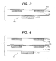
- FIG. 3 is a cross sectional diagram for describing the method of manufacturing the photoelectric conversion device illustrated in FIG. 1 .
- FIG. 4 is a cross sectional diagram for describing the method of manufacturing the photoelectric conversion device illustrated in FIG. 1 .
- FIG. 5 is a cross sectional diagram for describing the method of manufacturing the photoelectric conversion device illustrated in FIG. 1 .
- FIG. 6 is a cross sectional view of pixel region of a photoelectric conversion device according to a second exemplary embodiment of the present invention.
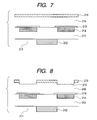
- FIG. 7 is a cross sectional diagram for describing the method of manufacturing the photoelectric conversion device illustrated in FIG. 6 .
- FIG. 8 is a cross sectional diagram for describing the method of manufacturing the photoelectric conversion device illustrated in FIG. 6 .
- FIG. 9 is a cross sectional diagram for describing the method of manufacturing the photoelectric conversion device illustrated in FIG. 6 .
- FIG. 10 is a cross sectional view of a photoelectric conversion device of a third exemplary embodiment of the present invention.
- FIG. 11 is a plane arrangement diagram of the photoelectric conversion device of the third exemplary embodiment of the present invention.
- FIG. 12 is a cross sectional diagram of a photoelectric conversion device of a fourth exemplary embodiment of the present invention.
- FIG. 13 is a cross sectional diagram of a modified example of the photoelectric conversion device of the fourth embodiment of the present invention.
- FIG. 1 illustrates a cross sectional structure of a photoelectric conversion device in the first exemplary embodiment of the present invention. It is to be noted that, in the description of the detailed configuration of the present embodiment and respective figures, description of element regions and element isolation areas, etc. formed on a semiconductor substrate will be omitted for simplifying the description.
- a semiconductor substrate 111 there are arranged plural photodiodes 112 each functioning as a photoelectric conversion element for performing photoelectric conversion.
- the region where such photoelectric conversion element is disposed is called a pixel region.
- a multilayered wiring structure including wiring layers 114, 117 buried in interlayer insulation films which will be described later is disposed over the semiconductor substrate 111.
- first interlayer insulation film 113 On the upper surface of the semiconductor substrate, there is disposed a first interlayer insulation film 113.
- first interlayer insulation film 113 there may be used silicon oxide film.
- the first wiring layer 114 is embedded in the first interlayer insulation film. This first wiring layer 114 is formed by forming a trench at the first interlayer insulation film 113 to bury conductor such as copper into this trench to remove conductor except for the trench part by the CMP process (damascene process).
- first diffusion suppressing film 115 for covering the first wiring layer, and for suppressing diffusion of material forming the first wiring.
- the diffusion suppressing film there may be used silicon nitride film or silicon carbide film. This first diffusion suppressing film 115 is configured so that the film body is selectively removed in the region corresponding to the photoelectric conversion element, and reflection of incident light at the interface between the interlayer insulation film and the diffusion suppressing film is thus reduced.
- a second interlayer insulation film 116 containing silicon oxide film is disposed on the first diffusion suppressing film 115.
- a second wiring layer 117 serving as the uppermost wiring layer is buried in the second interlayer insulation film 116 as a wiring layer disposed in the pixel region.
- This second wiring layer may be also formed by formation process similar to that of the first wiring layer.
- a silicon nitride film 118 is disposed on the upper part of the second wiring layer 117 as the second diffusion suppressing film. Further, inner-layer lenses 119 corresponding to each photoelectric conversion element is disposed in a region corresponding to the photoelectric conversion element on the second diffusion suppressing film. In addition, the silicon nitride film also functions as the second diffusion suppressing film and a protective film.
- diffusion suppressing film disposed on the uppermost wiring layer of the multilayered wiring structure is disposed also within a region corresponding to the photoelectric conversion element, and the lens utilizing the diffusion suppressing film is disposed.
- the lens may be disposed in the state directly in contact with the diffusion suppressing film by a layer different from the diffusion suppressing film. Since the diffusion suppressing film is disposed in a manner to cover a region corresponding to the photoelectric conversion element of the interlayer insulation film, an offset resulting from the fact that the diffusion suppressing film is removed does not takes place. As a result, a lens of such a configuration can be formed.
- the region corresponding to the photoelectric conversion element is a region corresponding to an optical path when light is incident on the photoelectric conversion device. Accordingly, the part which is not light-shielded by light shielding member corresponds to this region within the pixel region.
- a method of manufacturing the photoelectric conversion device in the present embodiment will now be described.
- the structure in which copper is used as wiring material and wire is buried in the interlayer insulation film will be described.
- plural semiconductor regions each functioning as electrode region of photoelectric conversion element 112 and transistor (not shown), and element isolation regions for isolating elements therebetween are formed over the semiconductor substrate.
- polysilicon (not shown) serving as gate electrode of transistor is formed on the semiconductor substrate, and silicon oxide film is deposited by the CVD process (Chemical Vapor Deposition) process. Thereafter, planarization is implemented by the CMP process (Chemical-Mechanical Polishing) process to thereby form first interlayer insulation film 113.
- CVD Chemical Vapor Deposition
- CMP Chemical-Mechanical Polishing
- first copper wires 114 are buried into the first interlayer insulation film by the damascene process ( FIG. 2 ).
- first diffusion suppressing film 115 is formed on the entire surface by silicon nitride film thereafter to remove the diffusion suppressing film 115 disposed in the region corresponding to the photoelectric conversion element by the lithography technology and the dry etching technology ( FIG. 3 ).
- the diffusion suppressing film 115 may be left as it is.
- silicon oxide film is formed by the CVD process to form a second interlayer insulation film 116.
- the second interlayer insulation film may be planarized by the CPM process.
- second wiring layer 117 serving as the uppermost wiring layer is formed by the damascene process within the pixel region ( FIG. 4 ). Further, silicon nitride film 118 functioning as a second diffusion suppressing film is formed by the CVD process. Since the second diffusion suppressing film is caused to function also as a protective film, the film thickness thereof is caused to be thicker than that of the first diffusion suppressing film to enhance protective function ( FIG. 5 ). Moreover, in order to enhance the protective characteristic, it is desirable to dispose the second diffusion suppressing film in a manner to cover the entire surface including an area corresponding to the photoelectric conversion element.
- inner-layer lens 119 is formed by using the lithography technology and the dry etching technology within a region corresponding to the photoelectric conversion element to thereby form the photoelectric conversion device of the present embodiment.
- a reflection prevention film may be used between the first interlayer insulation film 113 and the semiconductor substrate 111 in order to reduce reflection of incident light at the interface between the interlayer insulation film and the semiconductor substrate.
- the reflection prevention film there may be used, e.g., silicon nitride film.
- copper wiring may be formed by using either one of the single-damascene process, and the dual-damascene process, and the number of wiring layers is not limited to two.
- a convex lens is formed as the inner-layer lens 119
- a concave lens may be used.
- a silicon nitride film serving as a second diffusion suppressing film is thickly formed thereafter to transfer a resist pattern caused to have a lens shape with respect to the silicon nitride film.
- a portion of the silicon nitride film may be caused to have a lens shape.
- the present embodiment may be similarly applied to the structure in which color filter or micro lens is provided as occasion demands on the upper part of the inner-layer lens.
- the second diffusion suppressing film is not removed within the region corresponding to the photoelectric conversion element also in such a configuration, these members may be disposed without separately providing the interlayer insulation film or the planarized film. Thus, the height of the device can be reduced. Further, since the second diffusion suppressing film is disposed in a manner to cover the region corresponding to the photoelectric conversion element, the structure doubling as a protective film and a diffusion suppressing film can be provided. Thus, a process step of allowing the diffusion suppressing film to undergo patterning can be eliminated while maintaining the function as a protective layer.
- FIG. 6 is a cross sectional structural diagram of a photoelectric conversion device in the second exemplary embodiment of the present invention.
- the present embodiment is a modified embodiment of the first embodiment.
- a reflection prevention film (silicon oxynitride film).
- the silicon oxynitride film serves to suppress reflection of an incident light at the interface between the silicon oxide film 216 and the silicon nitride film 219. Accordingly, the reflection prevention film is not limited to silicon oxynitride film, but any material to reduce reflection at the interface may be employed.
- first forming first wiring layer 214 and subsequently forming first diffusion suppressing film 215 are similar to those of the first embodiment.
- silicon oxide film 216 is formed by the CVD process.
- planarization is performed by the CMP process.
- a silicon oxynitride film 218 is formed on the silicon oxide film 216 (interlayer insulation film) by the CVD process ( FIG. 7 ).
- double-layer structure (laminated structure) of the silicon oxide film 216 and the silicon oxynitride film 218 is formed.
- reflection prevention film to reduce reflection of an incident light at the interface between the interlayer insulation film and the diffusion suppressing film is formed on the interlayer insulation film.
- a laminated structure of the interlayer insulation film and the reflection preventing film is formed. Thereafter, etching is performed with respect to the region where wires are disposed of the double layer structure.
- wiring trenches 210 are formed ( FIG. 8 ).
- via hole portions may be also formed by etching (dual damascene).
- copper is formed at the wiring trenches 210 and via holes by plating to remove copper except for the trench 210 portions by the CMP process to thereby second wiring layer 217 ( FIG. 9 ).
- a silicon nitride film 219 functioning as protective film and diffusion preventing film for material of the second wiring layer.
- an inner-layer lens 220 is formed within the region corresponding to the photoelectric conversion element on the silicon nitride film 219.
- reflection prevention film 218 by silicon oxynitride film is disposed between the silicon oxide film forming the second interlayer insulation film 216 and the silicon nitride film 219 on the second wiring layer 217.
- reflection on the interface between the silicon oxide film 216 and the silicon nitride film 219 is suppressed. As a result, loss of light can be further reduced.
- the reflection prevention film is also etched simultaneously with the silicon oxide film.
- the process steps can be shortened.
- reflection preventing film can be formed within the entire of the region where wiring layer including a region corresponding to the light receiving unit of the photoelectric conversion element is not disposed (the region where no wiring trench is formed).
- FIGS. 10 and 11 are respectively a cross sectional diagram and a plane arrangement diagram of a photoelectric conversion device of a third exemplary embodiment of the present invention.
- the plane arrangement diagram of FIG. 11 will be first described.
- the photoelectric conversion device of the present embodiment includes a photoelectric conversion area 811.
- a unit of a signal which is read out from a single photoelectric conversion elements is caused to be a pixel, and the region where the photoelectric conversion element is disposed can be also called a pixel region.
- the pixel is the minimum unit of single photoelectric conversion element and element set for reading out a signal from the photoelectric conversion element to an output line.
- this element set there are included a transfer unit such as transfer MOS transistor, amplifier unit such as amplifier MOS transistor, and a reset unit such as reset MOS transistor. While, in adjacent photoelectric elements, those elements may be shared, the pixel is defined by the minimum unit of element set for reading out a signal of single photoelectric conversion element also in this case.
- the photoelectric conversion device further includes a signal processing circuit 812 for amplifying a signal which has been read out from the photoelectric conversion region.
- the signal processing circuit 812 is not limited to the amplifier circuit, but may be a circuit for removing noise of pixel by CDS processing.
- the signal processing circuit 812 may be a circuit for merely converting signals which are read out in parallel from plural train into a serial signal.
- the photoelectric conversion device further includes a vertical shift register 813 for driving MOS transistors disposed within the pixel area, and a horizontal shift register 814 for driving MOS transistors of the signal processing circuit.
- the circuit components 812 to 814 may be included within the peripheral circuit. The region where these circuit components are disposed is called a peripheral circuit region.
- peripheral circuits serve to control a signal output from the photoelectric conversion element.
- an AD conversion circuit may be included therewithin.
- the pixel region 811 and the peripheral circuits 812 to 814 are disposed over the same semiconductor substrate.
- a pixel region 312 where plural photodiodes 314 each functioning as a photoelectric conversion element are disposed in an array form.
- This pixel area 312 is a region corresponding to the pixel region 811 in FIG. 11 .
- a peripheral circuit 313 is also disposed on the same substrate. This peripheral circuit 313 corresponds to any one or all of the peripheral circuits 812 to 814 in FIG. 11 .
- the number of wiring layers of the pixel region is larger than the number of wiring layers of the peripheral circuit region.
- a method of manufacturing the photoelectric conversion device of the present embodiment will be described. Since the process steps up to formation of the second wiring layer 320 serving as the uppermost wiring layer of the pixel region may be implemented by using process steps of the first embodiment, etc., their description will be omitted.
- a silicon nitride film 321 serving to cover the second wiring layer 320 and functioning as a diffusion suppressing film.
- this first silicon nitride film 321 is caused to function as an interlayer insulation film.
- a first via plug 322 is formed at the first silicon nitride film 321 to further form a third wiring layer 323 within the peripheral circuit region 313.
- wiring material of the third wiring layer it is desirable to use aluminum. The reason why aluminum is used is that bonding pad for electrically connecting to the external is formed by way of the third wiring layer, and connection between bonding pad and wiring for taking electrical connection to the external device is thus easy as compared to copper.
- a protective film containing the second silicon nitride film 324 is formed on the third wiring layer 323.
- the pixel region is caused to be of the structure in which first silicon nitride film 321 and second silicon nitride film 324 are laminated.
- an inner-layer lens 325 is formed by the above-described transfer etching with respect to the laminated structure of the silicon nitride film.
- the silicon nitride film on the uppermost wiring layer of the pixel region is caused to double as a diffusion suppressing film and an interlayer insulation film of the peripheral circuit region.
- the process step of removing only the area corresponding to the photoelectric conversion element of the diffusion suppressing film can be omitted. As a result, it also becomes unnecessary to form interlayer insulation film necessary when the diffusion suppressing film has been removed. For this reason, the total film thickness on the photoelectric conversion element of the pixel region can be reduced. Further, by forming the inner-layer lens, incidence efficiency onto the light receiving unit can be enhanced.
- interlayer insulation film disposed between the second and third wiring layers serve as a silicon nitride film single layer within the peripheral circuit region, formation of via contact becomes easy.
- the first interlayer insulation film 316 is formed by depositing silicon oxide film by, e.g., the CVD process thereafter to planarize the silicon oxide film by the CMP process.
- first wiring layer 317 is buried at the first interlayer insulation film 316 by the damascene process. Further, the first diffusion suppressing film 318 is formed on the entire surface thereafter to remove the part on the light receiving unit by the lithography technology and the dry etching technology, etc.
- the first diffusion suppressing film 318 of the peripheral circuit region may be formed over the entire surface of the peripheral circuit region.
- the second interlayer insulation film 319 containing silicon oxide film is formed by, e.g., the CVD process.
- the second interlayer insulation film 319 may be planarized by the CMP process.
- the second wiring layer 320 serving as the uppermost wiring layer within the pixel area is formed by the damascene process.
- first silicon nitride film 321 functioning as diffusion suppressing film and third interlayer insulation film are formed by the CVD process.
- first via plug is formed at silicon nitride film 321 within the peripheral circuit region.
- third wiring layer 323 is formed thereafter to form second silicon nitride film 324 onto the entirety of the pixel region and the peripheral circuit area.
- the first and second silicon nitride films 321 and 324 which are laminated within the pixel region are used to form inner-layer lens 325 within a region corresponding to the photoelectric conversion element to thereby form a photoelectric conversion device in the present embodiment.
- the pixel region includes wiring layers of two layers, and the peripheral circuit region includes wiring layers of three layers.
- the number of wiring layers in the peripheral circuit region is larger than that in the pixel region.
- the peripheral circuit region is configured so as to include copper wiring layers of double layers and aluminum wiring layer of single layer.
- the number of wiring layers of the pixel region is not limited to be two.
- wiring material of the upper layer relative to the wiring layer disposed in the pixel region is not limited to aluminum.
- plural copper wirings may be formed through an intermediate insulation film formed by silicon nitride film on the upper layer relative to the uppermost wiring layer of the pixel area.
- the diffusion suppressing film disposed on the uppermost wiring layer of the pixel region has been described.
- the wiring layer except for the uppermost wiring layer of the multilayered wiring structure and its diffusion suppressing film will be described.
- FIG. 12 illustrates a cross sectional diagram of a photoelectric conversion device of the fourth embodiment of the present invention.
- a structure in which reflection prevention film is provided with respect to the configuration of the second embodiment, between diffusion suppressing film of wiring layer (e.g., first wiring layer) except for the uppermost wiring layer of the pixel region, and interlayer insulation film with which the diffusion suppressing film is in contact.
- this diffusion suppressing film is left without undergoing patterning also in the region corresponding to the photoelectric conversion element.
- a process step of performing patterning of the first diffusion suppressing film can be eliminated.
- facilitation of process can be realized.
- etching damage in etching the first diffusion suppressing film may be given to the photoelectric conversion element.
- the photoelectric conversion element of the present embodiment will be described with reference to FIG. 12 . Similar reference numerals are respectively attached to components similar to those of FIG. 6 , and their detailed description will be omitted.
- a first diffusion suppressing film 221 disposed on first wiring layer 214 is disposed in a manner to cover the entirety of the underlying film. Namely, there is employed a configuration in which first the diffusion suppressing film 221 is disposed also within a region corresponding to the photoelectric conversion element. Further, a reflection prevention film 222 is disposed within the region corresponding to the photoelectric conversion element 212 of the lower part of the first diffusion suppressing film 221. The reflection prevention film 222 may be formed by the same process as that of the second embodiment.
- FIG. 13 a modified example of the present embodiment is illustrated in FIG. 13 .
- the modified example differs from the fourth embodiment in that diffusion suppressing film 218 on the uppermost wiring layer of the pixel region and protective film 219 are formed by different constituent members.
- the present invention is not limited to these exemplary embodiments, but plural exemplary embodiments may be combined as occasion demands.
- the damascene process for burying wires into the interlayer insulation film has been described as the wiring formation process, but the wiring formation process is not limited to such damascene process.
- material having large diffusion coefficient, which is diffused within the interlayer insulation film such as, for example, copper is used as wiring material
- any photoelectric conversion device using diffusion suppressing material may be applied.
- wiring material is not limited to copper, but the present invention can be applied to the configuration using wiring material in which diffusion within the interlayer insulation film becomes problem.
- a photoelectric conversion device comprises a photoelectric conversion element disposed at a semiconductor substrate, and a multilayered wiring structure including a plurality of wiring layers disposed over the semiconductor substrate in such a manner to sandwich an interlayer insulation film therebetween.
- a diffusion suppressing film is disposed at least on the uppermost one of the wiring layers, the diffusion suppressing film serving to suppress diffusion of material forming the uppermost wiring layer; the diffusion suppressing film covers regions of the uppermost wiring layer and the interlayer insulation film corresponding to the photoelectric conversion element; and a lens is disposed with respect to a region of the diffusion suppressing film corresponding to the photoelectric conversion element.
Landscapes
- Solid State Image Pick-Up Elements (AREA)
- Engineering & Computer Science (AREA)
- Manufacturing & Machinery (AREA)
Applications Claiming Priority (1)
| Application Number | Priority Date | Filing Date | Title |
|---|---|---|---|
| JP2007044009A JP5159120B2 (ja) | 2007-02-23 | 2007-02-23 | 光電変換装置およびその製造方法 |
Publications (2)
| Publication Number | Publication Date |
|---|---|
| EP1962346A2 true EP1962346A2 (de) | 2008-08-27 |
| EP1962346A3 EP1962346A3 (de) | 2015-07-22 |
Family
ID=39535660
Family Applications (1)
| Application Number | Title | Priority Date | Filing Date |
|---|---|---|---|
| EP08151693.2A Withdrawn EP1962346A3 (de) | 2007-02-23 | 2008-02-20 | Photoelektrische Umwandlungsvorrichtung und Herstellungsverfahren dafür |
Country Status (5)
| Country | Link |
|---|---|
| US (2) | US20080203509A1 (de) |
| EP (1) | EP1962346A3 (de) |
| JP (1) | JP5159120B2 (de) |
| KR (1) | KR100963141B1 (de) |
| CN (2) | CN103219351A (de) |
Families Citing this family (8)
| Publication number | Priority date | Publication date | Assignee | Title |
|---|---|---|---|---|
| JP4110192B1 (ja) * | 2007-02-23 | 2008-07-02 | キヤノン株式会社 | 光電変換装置及び光電変換装置を用いた撮像システム |
| JP5288823B2 (ja) | 2008-02-18 | 2013-09-11 | キヤノン株式会社 | 光電変換装置、及び光電変換装置の製造方法 |
| JP5357441B2 (ja) | 2008-04-04 | 2013-12-04 | キヤノン株式会社 | 固体撮像装置の製造方法 |
| JP2010161236A (ja) | 2009-01-08 | 2010-07-22 | Canon Inc | 光電変換装置の製造方法 |
| JP5558916B2 (ja) * | 2009-06-26 | 2014-07-23 | キヤノン株式会社 | 光電変換装置の製造方法 |
| JP5563257B2 (ja) * | 2009-08-28 | 2014-07-30 | キヤノン株式会社 | 光電変換装置、撮像システム、及び光電変換装置の製造方法 |
| JP6029266B2 (ja) | 2011-08-09 | 2016-11-24 | キヤノン株式会社 | 撮像装置、撮像システムおよび撮像装置の製造方法 |
| JP7594488B2 (ja) | 2021-04-20 | 2024-12-04 | 株式会社東芝 | アイソレータ |
Citations (1)
| Publication number | Priority date | Publication date | Assignee | Title |
|---|---|---|---|---|
| JP2005311015A (ja) | 2004-04-21 | 2005-11-04 | Sony Corp | 固体撮像素子およびその製造方法 |
Family Cites Families (24)
| Publication number | Priority date | Publication date | Assignee | Title |
|---|---|---|---|---|
| US6221687B1 (en) * | 1999-12-23 | 2001-04-24 | Tower Semiconductor Ltd. | Color image sensor with embedded microlens array |
| KR100600945B1 (ko) * | 1999-12-28 | 2006-07-13 | 매그나칩 반도체 유한회사 | 광집적률 개선을 위한 이미지센서 |
| KR20010059238A (ko) * | 1999-12-30 | 2001-07-06 | 박종섭 | 광감도 개선을 위한 이미지센서 및 그 제조방법 |
| JP2001298175A (ja) * | 2000-04-12 | 2001-10-26 | Toshiba Corp | 撮像システム |
| JP4117672B2 (ja) * | 2002-05-01 | 2008-07-16 | ソニー株式会社 | 固体撮像素子及び固体撮像装置、並びにこれらの製造方法 |
| US6861686B2 (en) * | 2003-01-16 | 2005-03-01 | Samsung Electronics Co., Ltd. | Structure of a CMOS image sensor and method for fabricating the same |
| KR100499174B1 (ko) * | 2003-06-17 | 2005-07-01 | 삼성전자주식회사 | 이미지 소자 |
| JP4646577B2 (ja) * | 2004-09-01 | 2011-03-09 | キヤノン株式会社 | 光電変換装置、その製造方法及び撮像システム |
| US7453109B2 (en) * | 2004-09-03 | 2008-11-18 | Canon Kabushiki Kaisha | Solid-state image sensor and imaging system |
| JP4871499B2 (ja) * | 2004-09-03 | 2012-02-08 | キヤノン株式会社 | 固体撮像装置及び該固体撮像装置を用いた撮像システム |
| JP4725092B2 (ja) * | 2004-12-10 | 2011-07-13 | ソニー株式会社 | 固体撮像装置及びその製造方法 |
| KR20060077110A (ko) * | 2004-12-30 | 2006-07-05 | 매그나칩 반도체 유한회사 | 시모스 이미지센서 및 그의 제조방법 |
| JP4938238B2 (ja) * | 2005-01-07 | 2012-05-23 | ソニー株式会社 | 固体撮像素子及び固体撮像素子の製造方法 |
| KR100807214B1 (ko) * | 2005-02-14 | 2008-03-03 | 삼성전자주식회사 | 향상된 감도를 갖는 이미지 센서 및 그 제조 방법 |
| JP2006229206A (ja) * | 2005-02-14 | 2006-08-31 | Samsung Electronics Co Ltd | 向上された感度を有するイメージセンサ及びその製造方法 |
| JP2006261597A (ja) * | 2005-03-18 | 2006-09-28 | Canon Inc | 固体撮像装置、その製造方法及びカメラ |
| JP4944399B2 (ja) * | 2005-07-04 | 2012-05-30 | キヤノン株式会社 | 固体撮像装置 |
| KR100710207B1 (ko) * | 2005-09-22 | 2007-04-20 | 동부일렉트로닉스 주식회사 | 씨모스 이미지 센서의 제조방법 |
| JP2007242697A (ja) * | 2006-03-06 | 2007-09-20 | Canon Inc | 撮像装置および撮像システム |
| JP5110820B2 (ja) * | 2006-08-02 | 2012-12-26 | キヤノン株式会社 | 光電変換装置、光電変換装置の製造方法及び撮像システム |
| JP5087888B2 (ja) * | 2006-08-28 | 2012-12-05 | ソニー株式会社 | 固体撮像装置及びその製造方法 |
| JP5305622B2 (ja) * | 2006-08-31 | 2013-10-02 | キヤノン株式会社 | 光電変換装置の製造方法 |
| JP4315457B2 (ja) * | 2006-08-31 | 2009-08-19 | キヤノン株式会社 | 光電変換装置及び撮像システム |
| US7544982B2 (en) * | 2006-10-03 | 2009-06-09 | Taiwan Semiconductor Manufacturing Company, Ltd. | Image sensor device suitable for use with logic-embedded CIS chips and methods for making the same |
-
2007
- 2007-02-23 JP JP2007044009A patent/JP5159120B2/ja not_active Expired - Fee Related
-
2008
- 2008-02-06 US US12/026,627 patent/US20080203509A1/en not_active Abandoned
- 2008-02-20 EP EP08151693.2A patent/EP1962346A3/de not_active Withdrawn
- 2008-02-22 KR KR1020080016386A patent/KR100963141B1/ko not_active Expired - Fee Related
- 2008-02-22 CN CN2013100987894A patent/CN103219351A/zh active Pending
- 2008-02-22 CN CNA2008100808681A patent/CN101252137A/zh active Pending
-
2013
- 2013-03-15 US US13/836,492 patent/US20130203207A1/en not_active Abandoned
Patent Citations (1)
| Publication number | Priority date | Publication date | Assignee | Title |
|---|---|---|---|---|
| JP2005311015A (ja) | 2004-04-21 | 2005-11-04 | Sony Corp | 固体撮像素子およびその製造方法 |
Also Published As
| Publication number | Publication date |
|---|---|
| CN103219351A (zh) | 2013-07-24 |
| US20080203509A1 (en) | 2008-08-28 |
| JP2008210868A (ja) | 2008-09-11 |
| KR100963141B1 (ko) | 2010-06-15 |
| CN101252137A (zh) | 2008-08-27 |
| US20130203207A1 (en) | 2013-08-08 |
| KR20080078610A (ko) | 2008-08-27 |
| JP5159120B2 (ja) | 2013-03-06 |
| EP1962346A3 (de) | 2015-07-22 |
Similar Documents
| Publication | Publication Date | Title |
|---|---|---|
| US11689070B2 (en) | Solid-state imaging device, method of manufacturing solid-state imaging device, and electronic apparatus | |
| US20130203207A1 (en) | Photoelectric conversion device and method of manufacturing the same | |
| US7196365B2 (en) | Solid-state imaging device, solid-state imaging apparatus and methods for manufacturing the same | |
| JP5357441B2 (ja) | 固体撮像装置の製造方法 | |
| JP5760923B2 (ja) | 固体撮像装置の製造方法 | |
| JP5441382B2 (ja) | 光電変換装置及び光電変換装置の製造方法 | |
| US9966406B2 (en) | Semiconductor devices including back-side integrated circuitry | |
| JP5921129B2 (ja) | 固体撮像装置、及び固体撮像装置の製造方法 | |
| JP5709564B2 (ja) | 半導体装置の製造方法 | |
| US11488998B2 (en) | Semiconductor apparatus and equipment | |
| JP6083572B2 (ja) | 固体撮像装置及びその製造方法 | |
| JP2013026565A (ja) | 固体撮像装置、固体撮像装置の製造方法、および電子機器 | |
| JP5389208B2 (ja) | 光電変換装置 | |
| JP2005311015A (ja) | 固体撮像素子およびその製造方法 | |
| JP5329001B2 (ja) | 半導体装置の製造方法 | |
| JP2006294773A (ja) | 固体撮像素子及び固体撮像素子の製造方法 |
Legal Events
| Date | Code | Title | Description |
|---|---|---|---|
| PUAI | Public reference made under article 153(3) epc to a published international application that has entered the european phase |
Free format text: ORIGINAL CODE: 0009012 |
|
| AK | Designated contracting states |
Kind code of ref document: A2 Designated state(s): AT BE BG CH CY CZ DE DK EE ES FI FR GB GR HR HU IE IS IT LI LT LU LV MC MT NL NO PL PT RO SE SI SK TR |
|
| AX | Request for extension of the european patent |
Extension state: AL BA MK RS |
|
| PUAL | Search report despatched |
Free format text: ORIGINAL CODE: 0009013 |
|
| AK | Designated contracting states |
Kind code of ref document: A3 Designated state(s): AT BE BG CH CY CZ DE DK EE ES FI FR GB GR HR HU IE IS IT LI LT LU LV MC MT NL NO PL PT RO SE SI SK TR |
|
| AX | Request for extension of the european patent |
Extension state: AL BA MK RS |
|
| RIC1 | Information provided on ipc code assigned before grant |
Ipc: H01L 27/146 20060101AFI20150615BHEP |
|
| STAA | Information on the status of an ep patent application or granted ep patent |
Free format text: STATUS: THE APPLICATION HAS BEEN WITHDRAWN |
|
| 18W | Application withdrawn |
Effective date: 20151009 |