EP1951787B1 - Regioregular polyselenophenes - Google Patents
Regioregular polyselenophenes Download PDFInfo
- Publication number
- EP1951787B1 EP1951787B1 EP06828886A EP06828886A EP1951787B1 EP 1951787 B1 EP1951787 B1 EP 1951787B1 EP 06828886 A EP06828886 A EP 06828886A EP 06828886 A EP06828886 A EP 06828886A EP 1951787 B1 EP1951787 B1 EP 1951787B1
- Authority
- EP
- European Patent Office
- Prior art keywords
- meanings
- independently
- biselenophene
- alkyl
- mmol
- Prior art date
- Legal status (The legal status is an assumption and is not a legal conclusion. Google has not performed a legal analysis and makes no representation as to the accuracy of the status listed.)
- Not-in-force
Links
- 0 *c1c[s]cc1 Chemical compound *c1c[s]cc1 0.000 description 8
Images

Classifications
-
- C—CHEMISTRY; METALLURGY
- C08—ORGANIC MACROMOLECULAR COMPOUNDS; THEIR PREPARATION OR CHEMICAL WORKING-UP; COMPOSITIONS BASED THEREON
- C08G—MACROMOLECULAR COMPOUNDS OBTAINED OTHERWISE THAN BY REACTIONS ONLY INVOLVING UNSATURATED CARBON-TO-CARBON BONDS
- C08G61/00—Macromolecular compounds obtained by reactions forming a carbon-to-carbon link in the main chain of the macromolecule
- C08G61/12—Macromolecular compounds containing atoms other than carbon in the main chain of the macromolecule
- C08G61/122—Macromolecular compounds containing atoms other than carbon in the main chain of the macromolecule derived from five- or six-membered heterocyclic compounds, other than imides
- C08G61/123—Macromolecular compounds containing atoms other than carbon in the main chain of the macromolecule derived from five- or six-membered heterocyclic compounds, other than imides derived from five-membered heterocyclic compounds
-
- C—CHEMISTRY; METALLURGY
- C08—ORGANIC MACROMOLECULAR COMPOUNDS; THEIR PREPARATION OR CHEMICAL WORKING-UP; COMPOSITIONS BASED THEREON
- C08G—MACROMOLECULAR COMPOUNDS OBTAINED OTHERWISE THAN BY REACTIONS ONLY INVOLVING UNSATURATED CARBON-TO-CARBON BONDS
- C08G61/00—Macromolecular compounds obtained by reactions forming a carbon-to-carbon link in the main chain of the macromolecule
- C08G61/12—Macromolecular compounds containing atoms other than carbon in the main chain of the macromolecule
-
- C—CHEMISTRY; METALLURGY
- C08—ORGANIC MACROMOLECULAR COMPOUNDS; THEIR PREPARATION OR CHEMICAL WORKING-UP; COMPOSITIONS BASED THEREON
- C08G—MACROMOLECULAR COMPOUNDS OBTAINED OTHERWISE THAN BY REACTIONS ONLY INVOLVING UNSATURATED CARBON-TO-CARBON BONDS
- C08G79/00—Macromolecular compounds obtained by reactions forming a linkage containing atoms other than silicon, sulfur, nitrogen, oxygen, and carbon with or without the latter elements in the main chain of the macromolecule
-
- G—PHYSICS
- G06—COMPUTING; CALCULATING OR COUNTING
- G06K—GRAPHICAL DATA READING; PRESENTATION OF DATA; RECORD CARRIERS; HANDLING RECORD CARRIERS
- G06K19/00—Record carriers for use with machines and with at least a part designed to carry digital markings
-
- H—ELECTRICITY
- H10—SEMICONDUCTOR DEVICES; ELECTRIC SOLID-STATE DEVICES NOT OTHERWISE PROVIDED FOR
- H10K—ORGANIC ELECTRIC SOLID-STATE DEVICES
- H10K85/00—Organic materials used in the body or electrodes of devices covered by this subclass
- H10K85/10—Organic polymers or oligomers
- H10K85/111—Organic polymers or oligomers comprising aromatic, heteroaromatic, or aryl chains, e.g. polyaniline, polyphenylene or polyphenylene vinylene
- H10K85/113—Heteroaromatic compounds comprising sulfur or selene, e.g. polythiophene
-
- C—CHEMISTRY; METALLURGY
- C09—DYES; PAINTS; POLISHES; NATURAL RESINS; ADHESIVES; COMPOSITIONS NOT OTHERWISE PROVIDED FOR; APPLICATIONS OF MATERIALS NOT OTHERWISE PROVIDED FOR
- C09K—MATERIALS FOR MISCELLANEOUS APPLICATIONS, NOT PROVIDED FOR ELSEWHERE
- C09K2323/00—Functional layers of liquid crystal optical display excluding electroactive liquid crystal layer characterised by chemical composition
- C09K2323/02—Alignment layer characterised by chemical composition
-
- Y—GENERAL TAGGING OF NEW TECHNOLOGICAL DEVELOPMENTS; GENERAL TAGGING OF CROSS-SECTIONAL TECHNOLOGIES SPANNING OVER SEVERAL SECTIONS OF THE IPC; TECHNICAL SUBJECTS COVERED BY FORMER USPC CROSS-REFERENCE ART COLLECTIONS [XRACs] AND DIGESTS
- Y02—TECHNOLOGIES OR APPLICATIONS FOR MITIGATION OR ADAPTATION AGAINST CLIMATE CHANGE
- Y02E—REDUCTION OF GREENHOUSE GAS [GHG] EMISSIONS, RELATED TO ENERGY GENERATION, TRANSMISSION OR DISTRIBUTION
- Y02E10/00—Energy generation through renewable energy sources
- Y02E10/50—Photovoltaic [PV] energy
- Y02E10/549—Organic PV cells
Definitions
- the invention relates to regioregular polyselenophenes, to their use as semiconductors or charge transport materials, in optical, electro-optical or electronic devices, and to optical, electro-optical or electronic devices comprising them.
- OCV organic photovoltaics
- Polymers have found use in OPVs as they allow devices to be manufactured by solution-processing techniques such as spin casting, dip coating or ink jet printing. Solution processing can be carried out cheaper and on a larger scale compared to the evaporative techniques used to make inorganic thin film devices.
- solution-processing techniques such as spin casting, dip coating or ink jet printing.
- Solution processing can be carried out cheaper and on a larger scale compared to the evaporative techniques used to make inorganic thin film devices.
- polymer based devices are achieving efficiencies up to 4 - 5% (see for example K. M. Coakley and M. D. McGehee, Chem. Mater. 2004, 16, 4533-4542 ). This is appreciably lower than the efficiencies attainable by inorganic devices, which are typically up to 25%.
- P3AT poly(3-alkyl-thiophenes)
- P3HT poly(3-hexyl-thiophene)
- P3HT absorbs strongly over the range from 480 to 650 nm, with a peak maximum absorption at 560 nm. This means a significant portion of the light emitted by the sun is not being absorbed.
- polymers are required that absorb more light from the longer wavelength region (650 to 800 nm) of the solar spectra.
- polymers are desired which have a low band gap, preferably less than 1.9 eV, whereas for example P3HT has a band gap of ⁇ 2.0 eV.
- organic materials have also shown promise as the active layer in organic based thin film transistors and organic field effect transistors (TFT, OFET) (see H. E. Katz, Z. Bao and S. L. Gilat, Acc. Chem. Res., 2001, 34, 5, 359 ).
- TFT organic field effect transistor
- Such devices have potential applications in smart cards, security tags and the switching element in flat panel displays.
- Organic materials are envisaged to have substantial cost advantages over their silicon analogues if they can be deposited from solution, as this enables a fast, large-area fabrication route.
- the performance of the device is principally based upon the charge carrier mobility of the semi-conducting material and the current on/off ratio, so the ideal semiconductor should have a low conductivity in the off state, combined with a high charge carrier mobility (> 1 x 10 -3 cm 2 V -1 s -1 ).
- the semi-conducting material is relatively stable to oxidation i.e. it has a high ionisation potential, as oxidation leads to reduced device performance.
- a high regioregularity leads to improved packing and optimised microstructure, leading to improved charge carrier mobility [see H. Sirringhaus et al., Science, 1998, 280, 1741-1744 ; H. Sirringhaus et al., Nature, 1999, 401, 685-688 ; and H. Sirringhaus, et al., Synthetic Metals, 2000, 111-112, 129-132 ].
- P3AT show improved solubility and are able to be solution processed to fabricate large area films.
- P3AT have relatively low ionisation potentials and are susceptible to doping in air.
- Another aim of the invention is to provide new semiconductor and charge transport components, and new and improved electrooptical, electronic and luminescent devices comprising these components.
- Other aims of the invention are immediately evident to those skilled in the art from the following description.
- regioregular polyselenophenes as claimed in the present invention.
- P3AS regioregular poly(3-alkyl)selenophene
- other polymers containing selenophene exclusively in the backbone have bandgaps lower than 1.9 eV, whilst maintaining the desirable properties of high hole carrier transport, solution processablilty and high optical absorption coefficients.
- EP-A-1 439 590 discloses mono-, oligo- and poly-bis(thienyl) arylenes, but does not disclose the polymers of the present invention.
- S. Tierney, M. Heeney and I. McCulloch, Synth Met., 148(2), 195-198, (2005 ) discloses poly-bis(3-octyl-thiophen-2-yl) selenophene, but does not disclose polymers of the present invention.
- EP 0 902 043 A2 discloses substituted polyselenophenes. Bezoari et al., Journal of Polymer Science 19(7), 1981, pp-347-353 discloses polymers and copolymers of selenophene. Yoshino et al., Synt. Met. 10, 1985, pp-319-326 discloses the electrical and optical properties of a polyselenophene film. However, these documents do not disclose polymers as claimed in the present application.
- the invention relates to regioregular polymers of 2,5-selenophene that is optionally substituted in 3- and/or 4-position, as claimed in claim 1.
- the invention further relates to the use of the polymers according to the present invention as semiconducting, charge transport or light-emitting materials.
- the invention further relates to a semiconducting, electroluminescent or charge transport material, component or device comprising at least one polymer according to the present invention.
- the invention further relates to the use of polymers according to the present invention as charge-transport, semiconducting, electrically conducting, photoconducting or light-emitting material in optical, electrooptical or electronic components or devices, organic field effect transistors (OFET), integrated circuitry (IC), thin film transistors (TFT), flat panel displays, radio frequency identification (RFID) tags, electroluminescent or photoluminescent devices or components, organic light emitting diodes (OLED), backlights of displays, photovoltaic or sensor devices, charge injection layers, Schottky diodes, planarising layers, antistatic films, conducting substrates or patterns, electrode materials in batteries, photoconductors, electrophotographic applications, electrophotographic recording, organic memory devices, alignment layers, cosmetic or pharmaceutical compositions, biosensors, biochips, or for detecting and discriminating DNA sequences.
- OFET organic field effect transistors
- IC integrated circuitry
- TFT thin film transistors
- RFID radio frequency identification
- OLED organic light emitting diodes
- the invention further relates to an optical, electrooptical or electronic device, FET, integrated circuit (IC), TFT, OLED or alignment layer comprising a polymer, semiconducting or charge transport material, component or device according to the invention.
- the invention further relates to a TFT or TFT array for flat panel displays, radio frequency identification (RFID) tag, electroluminescent display or backlight comprising a polymer, semiconducting or charge transport material, component or device or a FET, IC, TFT or OLED according to the invention.
- RFID radio frequency identification
- the invention further relates to a security marking or device comprising a FET or an RFID tag according to the invention.
- regioregular means a polymer with a regioregularity of at least 85 %.
- Regioregularity means the number of head-to-tail couplings of monomer units in the polymer, divided by the number of total couplings, and expressed as a percentage.
- the molecular weight is given as the number average molecular weight M n or weight average molecular weight M n , determined by gel permeation chromatography (GPC) against polystyrene standards.
- the polymers of the present invention consist exclusively of 2,5-selenophene-diyl units that are optionally substituted in 3- and/or 4-position.
- regioregular P3AS has a reduced bandgap in comparison to regioregular P3AT. This makes the polyselenophenes of the present invention an attractive candidate as semiconducting material especially for use in photovoltaic devices. This result was surprising and could not be expected from the prior art, because prior art teaches that regiorandom P3HS has a larger bandgap than regiorandom P3HT (see Y. Katsumi et al Japanese Journal Appl. Physics. Part 2, 1989, 28, L138-L140 ).
- regioregular P3AS would also have a larger bandgap than regioregular P3AT, and thus would not be an attractive candidate for photovoltaics. This unexpectedly large reduction in bandgap on improving the regioregularity was not obvious.
- the high regioregularity in the polymers according to the present invention reduces steric interactions caused by head-head and tail-tail couplings, and allows the polymers to adopt a highly planar, organized lamellar structure.
- the polymers of the present invention are advantageous because they exhibit higher charge carrier mobilities compared to the analogous all-thiophene systems.
- the increased atomic radius of selenium (103 pm (picometre) over sulfur (88 pm) enhances molecular overlaps between polymer chains, and facilitates the charge hopping process.
- the polymers according to the invention are especially useful as charge transport or semiconductor materials, especially in OPV or OFET devices.
- Introduction of alkyl side chains into the selenophene group improves solubility and solution processibility of the polymers.
- the polymers according to the present invention can be homopolymers or copolymers.
- the polymers are selected of formula I wherein
- R 1-8 is aryl or heteroaryl, it is preferably a mono-, bi- or tricyclic aromatic or heteroaromatic group with up to 25 C atoms, wherein the rings can be fused.
- Heteroaromatic groups contain at least one hetero ring atom preferably selected from N, O and S.
- the aromatic or heteroaromatic groups are optionally substituted with one or more groups L.
- aryl and heteroaryl groups are phenyl, fluorinated phenyl, pyridine, pyrimidine, biphenyl, naphthalene, optionally fluorinated or alkylated or fluoroalkylated benzo[1,2-b:4,5-b']dithiophene, optionally fluorinated or alkylated or fluoroalkylated thieno[3,2-b]thiophene, optionally fluorinated or alkylated or fluoroalkylated 2,2-dithiophene, thiazole and oxazole, all of which are unsubstituted, mono- or polysubstituted with L as defined above.
- R 1-8 is an alkyl or alkoxy radical, i.e. where the terminal CH 2 group is replaced by -O-, this may be straight-chain or branched. It is preferably straight-chain, has 2 to 8 carbon atoms and accordingly is preferably ethyl, propyl, butyl, pentyl, hexyl, heptyl, octyl, ethoxy, propoxy, butoxy, pentoxy, hexyloxy, heptoxy, or octoxy, furthermore methyl, nonyl, decyl, undecyl, dodecyl, tridecyl, tetradecyl, pentadecyl, nonoxy, decoxy, undecoxy, dodecoxy, tridecoxy or tetradecoxy, for example.
- Fluoroalkyl or fluorinated alkyl or alkoxy is preferably straight chain (O)C i F 2i+1 , wherein i is an integer from 1 to 20, in particular from 1 to 15, very preferably (O)CF 3 , (O)C 2 F 5 , (O)C 3 F 7 , (O)C 4 F 9 , (O)C 5 F 11 , (O)C 6 F 13 , (O)C 7 F 5 or (O)C 8 F 17 , most preferably (O)C 6 F 13 .
- Halogen is preferably F, Br or Cl.
- Hetero atoms are preferably selected from N, O and S.
- the polymerisable group P is a group that is capable of participating in a polymerisation reaction, like radicalic or ionic chain polymerisation, polyaddition or polycondensation, or capable of being grafted, for example by condensation or addition, to a polymer backbone in a polymeranaloguous reaction.
- a polymerisation reaction like radicalic or ionic chain polymerisation, polyaddition or polycondensation, or capable of being grafted, for example by condensation or addition, to a polymer backbone in a polymeranaloguous reaction.
- polymerisable groups for chain polymerisation reactions like radicalic, cationic or anionic polymerisation.
- Very preferred are polymerisable groups comprising a C-C double or triple bond, and polymerisable groups capable of polymerisation by a ring-opening reaction, like oxetanes or epoxides.
- Oxetanes produce less shrinkage upon polymerisation (cross-linking), which results in less stress development within films, leading to higher retention of ordering and fewer defects.
- Oxetane cross-linking also requires cationic initiator, which unlike free radical initiator is inert to oxygen.
- spacer group Sp all groups can be used that are known for this purpose to the skilled in the art.
- the spacer group Sp is preferably of formula Sp'-X, such that P-Sp- is P-Sp'-X- and P*-Sp- is P*-Sp'-X-, wherein
- Typical groups Sp' are, for example, -(CH 2 ) p -, -(CH 2 CH 2 O) q -CH 2 CH 2 -, - CH 2 CH 2 -S-CH 2 CH 2 - or -CH 2 CH 2 -NH-CH 2 CH 2 - or -(SiR 0 R 00 -O) p -, with p being an integer from 2 to 12, q being an integer from 1 to 3 and R 0 and R 00 having the meanings given above.
- Preferred groups Sp' are ethylene, propylene, butylene, pentylene, hexylene, heptylene, octylene, nonylene, decylene, undecylene, dodecylene, octadecylene, ethyleneoxyethylene, methyleneoxybutylene, ethylene-thioethylene, ethylene-N-methyl-iminoethylene, 1-methylalkylene, ethenylene, propenylene and butenylene for example.
- each of the groups P or P* and the spacer groups Sp can be identical or different.
- P*-Sp- Another preferred embodiment relates to compounds comprising one or more groups P*-Sp-, wherein P* is a group that can be converted to or substituted by a polymerisable group P as defined above.
- P* is a group that is less reactive than P, for example towards spontaneous polymerisation.
- These compounds can be used for example as intermediates in the synthesis of polymerisable compounds of formula I having one or more groups P, or as a precursor material for polymerisable compounds which are too reactive to be stored or transported for longer periods of time.
- the group P* is preferably chosen such that it can easily be transformed into or substituted by a group P by known methods. For example, it can be a protected form of group P.
- P* are for example -OH or silyl groups like -O-Si-R 0 R 00 R 000 , for example - O-Si(CH 3 ) 3 , -O-Si-(isopropyl) 3 , -O-Si-(phenyl) 3 , -O-Si-(CH 3 ) 2 (phenyl), -O-Si(CH 3 ) 2 (tert-butyl) or the like, which can be reacted e.g. into polymerisable (meth)acrylate end groups.
- SCLCPs obtained from the inventive compounds or mixtures by polymerisation or copolymerisation have a backbone that is formed by the polymerisable group P.
- the polymers of the present invention can be synthesized according to or in analogy to methods that are known to the skilled person and are described in the literature. Other methods of preparation can be taken from the examples. Some preferred methods are described below (wherein R has one of the meanings of R 1 , and X has one of the meanings of X 1 , as given above).
- 3-Hexylselenophene is prepared according to the literature procedure ( C. Mahatsekake et al, Phosphorus, Sulfur and Silicon, 1990, 47, 35-41 ). The material is brominated in the 2,5-positions by treatment with NBS in THF.
- the resulting 2,5-dibromo-3-hexylselenophene is treated with 1 equivalent of an alkyl grignard reagent (for example iso-propyl magnesium chloride), to form, via a grignard metathesis reaction, a mixture of 2-bromo-5-chloromagnesium-3-hexylselenophene and 2-chloromagnesium-5-bromo-3-hexylselenophene in solution.
- the resulting mixture is polymerised directly by addition of a transition metal catalyst, to afford regioregular poly(3-hexyl)selenophene.
- Ni(II) salts such as Ni(dppp)Cl 2 (1,3-bis(diphenylphosphinopropane) nickel(II) chloride), Ni(dppe)Cl 2 (1,2-bis(diphenylphosphino)ethane nickel(II) chloride) or Ni(dppf)Cl 2 ⁇ dichloro[1,1'-bis(diphenylphosphino)ferrocene] nickel(II) ⁇ , or Ni(0) catalysts, for example bis(1,5-cyclooctadiene)nickel (0) [Ni(COD) 2 ], in the presence of a bidentate ligand, for example a phosphine ligand like 1,3-diphenylphosphinopropane (dppp).
- Ni(II) salts such as Ni(dppp)Cl 2 (1,3-bis(diphenylphosphinopropane) nickel(II) chloride), Ni(dppe)C
- catalysts are palladium (0) catalysts such as Pd(PPh 3 ) 4 (tetrakis(triphenylphosphine)palladium (0)) or Pd 2 (dba) 3 (tris(dibenzylideneacetone)dipalladium (0)) or palladium (II) precursors such as Pd(PPh 3 )Cl 2 (dichlorobis(triphenylphosphine)palladium (II)), or Pd(dppf)Cl 2 (dichloro[1,1'-bis(diphenylphosphino)ferrocene]palladium (II), optionally in the presence of additional phosphine ligands) affords the desired polymers.
- palladium (0) catalysts such as Pd(PPh 3 ) 4 (tetrakis(triphenylphosphine)palladium (0)) or Pd 2 (dba) 3 (tris(dibenzylideneacetone
- Such polymers can be prepared by reaction of 5,5'-dibromo-4,4'-dialkyl-2,2'-biselenophene with the bis(boronic) acids or esters of selenophene and biselenophene (Suzuki polymerisation) in the presence of a transition metal catalyst and a base.
- the polymers can also be prepared by polymerisation of a preformed tri-or tetraselenophene monomer via oxidative coupling, as exemplarily illustrated in Scheme 3.
- a further aspect of the invention relates to both the oxidised and reduced form of the compounds and materials according to this invention. Either loss or gain of electrons results in formation of a highly delocalised ionic form, which is of high conductivity. This can occur on exposure to common dopants. Suitable dopants and methods of doping are known to those skilled in the art, e.g. from EP 0 528 662 , US 5,198,153 or WO 96/21659 .
- the doping process typically implies treatment of the semiconductor material with an oxidating or reducing agent in a redox reaction to form delocalised ionic centres in the material, with the corresponding counterions derived from the applied dopants.
- Suitable doping methods comprise for example exposure to a doping vapor in the atmospheric pressure or at a reduced pressure, electrochemical doping in a solution containing a dopant, bringing a dopant into contact with the semiconductor material to be thermally diffused, and ion-implantantion of the dopant into the semiconductor material.
- suitable dopants are for example halogens (e.g., I 2 , Cl 2 Br 2 , ICl, ICl 3 , lBr and IF), Lewis acids (e.g., PF 5 , AsF 5 , SbF 5 , BF 3 , BCl 3 , SbCl 5 , BBr 3 and SO 3 ), protonic acids, organic acids, or amino acids (e.g., HF, HCl, HNO 3 H 2 SO 4 , HClO 4 , FSO 3 H and ClSO 3 H), transition metal compounds (e.g., FeCl 3 , FeOCl, Fe(ClO 4 ) 3 , Fe(4-CH 3 C 6 H 4 SO 3 ) 3 , TiCl 4 , ZrCl 4 , HfCl 4 , NbF 5 , NbCl 5 , TaCl 5 , MoF 5 , MoCl 5 , WF 5 ,
- halogens e
- examples of dopants are cations (e.g., H + , Li + , Na + , K + , Rb + and Cs + ), alkali metals (e.g., Li, Na, K, Rb, and Cs), alkaline-earth metals (e.g., Ca, Sr, and Ba), O 2 , XeOF 4 , (NO 2 + ) (SbF 6 - ), (NO 2 + ) (SbCl 6 - ), (NO 2 + ) (BF 4 - ), AgClO 4 , H 2 lrCl 6 , La(NO 3 ) 3 6H 2 O, FSO 2 OOSO 2 F, Eu, acetylcholine, R 4 N + , (R is an alkyl group), R 4 P + (R is an alkyl group), R 6 As + (R is an alkyl group), and R 3 S + (R is an alkyl group).
- dopants are cations
- the conducting form of the compounds and materials of the present invention can be used as an organic "metal" in applications, for example, but not limited to, charge injection layers and ITO planarising layers in organic light emitting diode applications, films for flat panel displays and touch screens, antistatic films, printed conductive substrates, patterns or tracts in electronic applications such as printed circuit boards and condensers.
- a preferred embodiment of the present invention relates to compounds of formula I and 11 and their preferred subformulae that are mesogenic or liquid crystalline, and very preferably comprise one or more polymerisable groups.
- Very preferred materials of this type are oligomers of formula I or I1 and their preferred subformulae wherein n is an integer from >1 to 15 and R 9 and/or R 10 denote P-Sp-.
- These materials are particularly useful as semiconductors or charge transport materials, as they can be aligned into uniform highly ordered orientation in their liquid crystal phase by known techniques, thus exhibiting a higher degree of order that leads to particularly high charge carrier mobility.
- the highly ordered liquid crystal state can be fixed by in situ polymerisation or crosslinking via the groups P to yield polymer films with high charge carrier mobility and high thermal, mechanical and chemical stability.
- the liquid crystal material preferably comprises one or more compounds of formula 11 and its preferred subformulae wherein one or both of R 9 and R 10 denote P-Sp-.
- the polymer is preferably made from a liquid crystal material comprising one or more compounds of formula I1 and its preferred subformulae wherein one of R 9 and R 10 denotes P-Sp-.
- another aspect of the invention relates to a polymerisable liquid crystal material comprising one or more compounds of the present invention as described above and below comprising at least one polymerisable group, and optionally comprising one or more further polymerisable compounds, wherein at least one of the polymerisable compounds of the present invention and/or the further polymerisable compounds is mesogenic or liquid crystalline.
- liquid crystal materials having a nematic and/or smectic phase.
- smectic materials are especially preferred.
- OLED applications nematic or smectic materials are especially preferred.
- smectic A (S A ) phases are especially preferred.
- S A smectic A phases, furthermore highly ordered smectic phases like the S B , S E , S G and S F phase.
- Another aspect of the present invention relates to an anisotropic polymer film with charge transport properties obtainable from a polymerisable liquid crystal material as defined above that is aligned in its liquid crystal phase into macroscopically uniform orientation and polymerised or crosslinked to fix the oriented state.
- polymerisation is carried out as in-situ polymerisation of a coated layer of the material, preferably during fabrication of the electronic or optical device comprising the inventive semiconductor material.
- these are preferably aligned in their liquid crystal state into homeotropic orientation prior to polymerisation, where the conjugated pi-electron systems are orthogonal to the direction of charge transport. This ensures that the intermolecular distances are minimised and hence then energy required to transport charge between molecules is minimised.
- the molecules are then polymerised or crosslinked to fix the uniform orientation of the liquid crystal state. Alignment and curing are carried out in the liquid crystal phase or mesophase of the material. This technique is known in the art and is generally described for example in D.J. Broer, et al., Angew. Makromol. Chem. 183, (1990), 45-66
- Alignment of the liquid crystal material can be achieved for example by treatment of the substrate onto which the material is coated, by shearing the material during or after coating, by application of a magnetic or electric field to the coated material, or by the addition of surface-active compounds to the liquid crystal material.
- Reviews of alignment techniques are given for example by I. Sage in "Thermotropic Liquid Crystals", edited by G. W. Gray, John Wiley & Sons, 1987, pages 75-77 , and by T. Uchida and H. Seki in “Liquid Crystals - Applications and Uses Vol. 3", edited by B. Bahadur, World Scientific Publishing, Singapore 1992, pages 1-63 .
- a review of alignment materials and techniques is given by J. Cognard, Mol. Cryst. Liq. Cryst. 78, Supplement 1 (1981), pages 1-77 .
- Actinic radiation means irradiation with light, like UV light, IR light or visible light, irradiation with X-rays or gamma rays or irradiation with high energy particles, such as ions or electrons.
- Preferably polymerisation is carried out by UV irradiation at a non-absorbing wavelength.
- a source for actinic radiation for example a single UV lamp or a set of UV lamps can be used. When using a high lamp power the curing time can be reduced.
- Another possible source for actinic radiation is a laser, like e.g. a UV laser, an IR laser or a visible laser.
- Polymerisation is preferably carried out in the presence of an initiator absorbing at the wavelength of the actinic radiation.
- an initiator absorbing at the wavelength of the actinic radiation.
- a photoinitiator can be used that decomposes under UV irradiation to produce free radicals or ions that start the polymerisation reaction.
- a radical photoinitiator is used
- curing polymerisable materials with vinyl, epoxide and oxetane groups preferably a cationic photoinitiator is used.
- a polymerisation initiator that decomposes when heated to produce free radicals or ions that start the polymerisation.
- a photoinitiator for radical polymerisation for example the commercially available Irgacure 651, Irgacure 184, Darocure 1173 or Darocure 4205 (all from Ciba Geigy AG) can be used, whereas in case of cationic photopolymerisation the commercially available UVI 6974 (Union Carbide) can be used.
- the polymerisable material can additionally comprise one or more other suitable components or additives selected for example from catalysts, sensitizers, stabilizers, inhibitors, chain-transfer agents, co-reacting monomers, surface-active compounds, lubricating agents, wetting agents, dispersing agents, hydrophobing agents, adhesive agents, flow improvers, defoaming agents, deaerators, diluents, reactive diluents, auxiliaries, colourants, dyes, pigments or nanoparticles.
- suitable components or additives selected for example from catalysts, sensitizers, stabilizers, inhibitors, chain-transfer agents, co-reacting monomers, surface-active compounds, lubricating agents, wetting agents, dispersing agents, hydrophobing agents, adhesive agents, flow improvers, defoaming agents, deaerators, diluents, reactive diluents, auxiliaries, colourants, dyes, pigments or nanoparticles.
- Compounds comprising one or more groups P-Sp- can also be copolymerised with polymerisable mesogenic compounds to induce or enhance liquid crystal phase behaviour.
- Polymerisable mesogenic compounds that are suitable as comonomers are known in prior art and disclosed for example in WO 93/22397 ; EP 0,261,712 ; DE 195,04,224 ; WO 95/22586 and WO 97/00600 .
- SCLCP liquid crystal side chain polymer
- SCLCPs obtained from one or more compounds of formula 11 and its preferred subformulae wherein n is an integer from >1 to 15 and one or both, preferably one, of R 9 and R 10 are a polymerisable or reactive group, or from a polymerisable mixture comprising one or more of said compounds.
- Another aspect of the invention relates to an SCLCP obtained from one or more compounds of formula I1 and its preferred subformulae wherein n is an integer from >1 to 15 and one or both of R 9 and R 10 are a polymerisable group, or from a polymerisable liquid crystal mixture as defined above, by copolymerisation or polymeranaloguous reaction together with one or more additional mesogenic or non-mesogenic comonomers.
- SCLCPs Side chain liquid crystal polymers or copolymers
- the semiconducting component in which the semiconducting component is located as a pendant group, separated from a flexible backbone by an aliphatic spacer group, offer the possibility to obtain a highly ordered lamellar like morphology.
- This structure consists of closely packed conjugated aromatic mesogens, in which very close (typically ⁇ 4 A) pi-pi stacking can occur. This stacking allows intermolecular charge transport to occur more easily, leading to high charge carrier mobilities.
- SCLCPs are advantageous for specific applications as they can be readily synthesized before processing and then e.g. be processed from solution in an organic solvent. If SCLCPs are used in solutions, they can orient spontaneously when coated onto an appropriate surface and when at their mesophase temperature, which can result in large area, highly ordered domains.
- SCLCPs can be prepared from the polymerisable compounds or mixtures according to the invention by the methods described above, or by conventional polymerisation techniques which are known to those skilled in the art, including for example radicalic, anionic or cationic chain polymerisation, polyaddition or polycondensation. Polymerisation can be carried out for example as polymerisation in solution, without the need of coating and prior alignment, or polymerisation in situ. It is also possible to form SCLCPs by grafting compounds according to the invention with a suitable reactive group, or mixtures thereof, to presynthesized isotropic or anisotropic polymer backbones in a polymeranaloguous reaction.
- compounds with a terminal hydroxy group can be attached to polymer backbones with lateral carboxylic acid or ester groups, compounds with terminal isocyanate groups can be added to backbones with free hydroxy groups, compounds with terminal vinyl or vinyloxy groups can be added, e.g., to polysiloxane backbones with Si-H groups. It is also possible to form SCLCPs by copolymerisation or polymeranaloguous reaction from the inventive compounds together with conventional mesogenic or non mesogenic comonomers. Suitable comonomers are known to those skilled in the art.
- Typical mesogenic comonomers are for example those mentioned in WO 93/22397 , EP 0 261 712 , DE 195 04 224 , WO 95/22586 , WO 97/00600 and GB 2 351 734 .
- Typical non mesogenic comonomers are for example alkyl acrylates or alkyl methacrylates with alkyl groups of 1 to 20 C atoms, like methyl acrylate or methyl methacrylate.
- the compounds of the present invention are useful as optical, electronic and semiconductor materials, in particular as charge transport materials in field effect transistors (FETs), e.g., as components of integrated circuitry, ID tags or TFT applications.
- FETs field effect transistors
- they may be used in organic light emitting diodes (OLEDs) in electroluminescent display applications or as backlight of, e.g., liquid crystal displays, as photovoltaics or sensor materials, for electrophotographic recording, and for other semiconductor applications.
- OLEDs organic light emitting diodes
- oligomers and polymers according to the invention show advantageous solubility properties which allow production processes using solutions of these compounds.
- films, including layers and coatings may be generated by low cost production techniques, e.g., spin coating.
- Suitable solvents or solvent mixtures comprise alkanes and/ or aromatics, especially their fluorinated derivatives.
- the materials of the present invention are useful as optical, electronic and semiconductor materials, in particular as charge transport materials in field effect transistors (FETs), as photovoltaics or sensor materials, for electrophotographic recording, and for other semiconductor applications.
- FETs field effect transistors
- Such FETs where an organic semiconductive material is arranged as a film between a gate-dielectric and a drain and a source electrode, are generally known, e.g., from US 5,892,244 , WO 00/79617 , US 5,998,804 , and from the references cited in the background and prior art chapter and listed below. Due to the advantages, like low cost production using the solubility properties of the compounds according to the invention and thus the processibility of large surfaces, preferred applications of these FETs are such as integrated circuitry, TFT-displays and security applications.
- field effect transistors and other devices with semiconductive materials may be used for ID tags or security markings to authenticate and prevent counterfeiting of documents of value like banknotes, credit cards or ID cards, national ID documents, licenses or any product with monetry value, like stamps, tickets, shares, cheques etc..
- the compounds according to the invention may be used in organic light emitting devices or diodes (OLEDs), e.g., in display applications or as backlight of e.g. liquid crystal displays.
- OLEDs organic light emitting devices or diodes
- Common OLEDs are realized using multilayer structures.
- An emission layer is generally sandwiched between one or more electron-transport and/ or hole-transport layers.
- By applying an electric voltage electrons and holes as charge carriers move towards the emission layer where their recombination leads to the excitation and hence luminescence of the lumophor units contained in the emission layer.
- the inventive compounds, materials and films may be employed in one or more of the charge transport layers and/ or in the emission layer, corresponding to their electrical and/ or optical properties.
- the compounds, materials and films according to the invention show electroluminescent properties themselves or comprise electroluminescent groups or compounds.
- the selection, characterization as well as the processing of suitable monomeric, oligomeric and polymeric compounds or materials for the use in OLEDs is generally known by a person skilled in the art, see, e.g., Meerholz, Synthetic Materials, 111-112, 2000, 31-34 , Alcala, J. Appl. Phys., 88, 2000, 7124-7128 and the literature cited therein.
- inventive compounds, materials or films especially those which show photoluminescent properties, may be employed as materials of light sources, e.g., of display devices such as described in EP 0 889 350 A1 or by C. Weder et al., Science, 279, 1998, 835-837 .
- inventive compounds, materials or films can be used alone or together with other materials in or as alignment layers in LCD or OLED devices, as described for example in US 2003/0021913 .
- charge transport compounds according to the present invention can increase the electrical conductivity of the alignment layer.
- this increased electrical conductivity can reduce adverse residual dc effects in the switchable LCD cell and suppress image sticking or, for example in ferroelectric LCDs, reduce the residual charge produced by the switching of the spontaneous polarisation charge of the ferroelectric LCs.
- this increased electrical conductivity can enhance the electroluminescence of the light emitting material.
- the compounds or materials according to the present invention having mesogenic or liquid crystalline properties can form oriented anisotropic films as described above, which are especially useful as alignment layers to induce or enhance alignment in a liquid crystal medium provided onto said anisotropic film.
- the materials according to the present invention may also be combined with photoisomerisable compounds and/or chromophores for use in or as photoalignment layers, as described in US 2003/0021913 .
- the compounds and materials according to the present invention can be employed as chemical sensors or materials for detecting and discriminating DNA sequences.
- Such uses are described for example in L. Chen, D. W. McBranch, H. Wang, R. Helgeson, F. Wudl and D. G. Whitten, Proc. Natl. Acad. Sci. U.S.A. 1999, 96, 12287 ; D. Wang, X. Gong, P. S. Heeger, F. Rininsland, G. C. Bazan and A. J. Heeger, Proc. Natl. Acad. Sci. U.S.A.
- the compounds and materials according to the present invention can also be used in cosmetic or pharmaceutical compositions, for example in cosmetic compositions for hair treatment as disclosed in EP 1 498 112 A2 .
- Polymer 1 is prepared as described below:
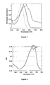
- Figure 1 shows UV-Vis spectra of polymer 1 (prepared according to the first method) in chlorobenzene (a) and as a thin film (b).
- Regioregular poly(3-hexyl)thiophene in chlorobenzene (c) and as a thin film (d) is shown for comparison
- the P3HT has a regioregularity of 96% and is available from the Aldrich chemical company.
- P3HS shows a red shift both in maximum absorbance and absorption onset in comparison to P3HT indicating the P3HS has a smaller bandgap than P3HT.
- Polymer 2 is prepared as follows:
- Step 2-1 2,5-dibromo-3-octylselenophene
- Step 2-2 Poly-3-octylselenophene
- Polymer (3) is prepared as follows:
- 3-Decylselenophene (0.92 g, 3.4 mmol) is dissolved in THF (20 ml), followed by the addition of N-bromosuccinimide (1.2 g, 6.7 mmol) in portions over 10 min at 0°C. After complete addition, the mixture is allowed to warm to 16-18°C and stirred in dark under nitrogen overnight (-16 h). Then water is added and the mixture is extracted with ethyl acetate (3 ⁇ 50 ml). The combined extracts are washed with water and brine then dried over Na 2 SO 4 . The solvent is removed under reduced pressure. The residue is purified by column chromatography on silica, eluting with petrol, to give a pale yellow oil (1.27 g, 87%).
- Step 3.2 Poly(3-decyl)selenophene:
- Polymer 4 is prepared as described below:
- the reaction is stirred at 25°C for a further 16 h, and quenched by the addition of 5% HCl (50 ml).
- the organics are extracted with ethyl acetate (3 x 50 ml).
- the combined organics are washed with 5% HCl (2 x 50 ml), water (50 ml) and saturated sodium chloride (50 ml), dried (Na 2 SO 4 ), filtered and concentrated under reduced pressure.
- the resulting oil is further purified by column chromatography over silica (eluant: petrol 40-60°C). The first fraction contained 3-hexylselenophene and the second fraction contained the product.
- a 10 ml glass vial is charged with a stirrer bar, 5,5'-dibromo-4,4'-bis(hexyl)-2,2'-biselenophene (150 mg, 0.256 mmol), 2,5-bis-trimethylstannylselenophene (116.9 mg, 0.256 mmol), tris(dibenzylideneacetone)dipalladium (0) (4.7 mg, 0.005 mmol, 4 mol % Pd), tri(o-tolyl)phosphine (6.2 mg, 0.02 mmol, 8 mol %) and chlorobenzene (5 ml).
- the glass vial is purged with nitrogen and securely sealed.
- the glass vial is placed into a microwave reactor (Emrys Creator, Personal Chemistry Ltd) and heated sequentially to 140°C for 2 min, then 160°C for 2 min and finally to 180°C for 15 min. After cooling to RT, the reaction mixture is precipitated into a mixture of methanol (50 mL) and 37% hydrochloric acid (5 mL), and stirred for 14 h. The polymer is filtered, washed (via Soxhlet extraction) with methanol (6 h), acetone (24 h) and isohexane (24 h).
- Polymer 5 is prepared as described below:
- the reaction is stirred at 25°C for a further 16 h, and quenched by the addition of 5% HCl (50 ml).
- the organics are extracted with ethyl acetate (3 x. 100 ml).
- the combined organics are washed with 5% HCl (2 x 80 ml), water (80 ml) and saturated sodium chloride (80 ml), dried (Na 2 SO 4 ), filtered and concentrated under reduced pressure.
- the resulting oil is further purified by column chromatography over silica (eluent: petrol 40-60°C). The first fraction contained 3-octylselenophene and the second fraction contained the product.
- a 10 ml glass vial is charged with a stirrer bar, 5,5'-dibromo-4,4'-bis(hexyl)-2,2'-biselenophene (328.7 mg, 0.512 mmol), 2,5-bis-trimethylstannylselenophene (233.7 mg, 0.512 mmol), tris(dibenzylideneacetone)dipalladium (0) (9.37 mg, 0.01 mmol, 4 mol % Pd), tri(o-tolyl)phosphine (12.46 mg, 0.04 mmol, 8 mol %) and chlorobenzene (8 ml).
- the glass vial is purged with nitrogen and securely sealed.
- the glass vial is placed into a microwave reactor (Emrys Creator, Personal Chemistry Ltd) and heated sequentially to 140°C for 2 min, then 160°C for 2 min and finally to 180°C for 15 min. After cooling to RT, the reaction mixture is precipitated into a mixture of methanol (50 mL) and 37% hydrochloric acid (5 mL), and stirred for 14 h. The polymer is filtered, washed (via Soxhlet extraction) with methanol (6 h), acetone (24 h) and isohexane (24 h). The resulting polymer is dissolved in hot chloroform and precipitated into methanol to afford the product (180 mg).
- a microwave reactor Emrys Creator, Personal Chemistry Ltd
- Polymer 6 is prepared as described below:
- 3-Decylselenophene is prepared according to the published procedure ( C. Mahatsekake et al, Phosphorus, Sulfur and Silicon, 1990, 47, 35-41 ; 1.0 g, 4.64 mmol).
- the resulting solution is cooled to -20°C and copper(II) chloride (2.96 g, 22 mmol) is added at once as a solid.
- the reaction is stirred at 25°C for a further 16 h, and quenched by the addition of 5% HCl (50 ml).
- the organics are extracted with ethyl acetate (3 x 100 ml).
- the combined organics are washed with 5% HCl (2 x 80 ml), water (80 ml) and saturated sodium chloride (80 ml), dried (Na 2 SO 4 ), filtered and concentrated under reduced pressure.
- the resulting oil is further purified by column chromatography over silica (eluant: petrol 40-60°C).
- the first fraction contained 3-decylselenophene and the second fraction contained the product. Recrystallisation from diethyl ether affords the product as a white solid (2.6 g, 52%). Mpt 56.5-57.0°C. M/Z 542 (M+).
- 1 H NMR 300 MHz, CDCl 3 ) ⁇ 7.35 (s, 2H), 7.10 (s, 2H), 2.52 (t, 4H), 1.60 (quint, 4H), 1.30 (m, 28H), 0.88 (t, 6H).
- a 10 ml glass vial is charged with a stirrer bar, 5,5'-dibromo-4,4'-bis(decyl)-2,2'-biselenophene (400 mg, 0.573 mmol), 2,5-bis-trimethylstannylselenophene (261.5 mg, 0.573 mmol), tris(dibenzylideneacetone)dipalladium (0) (10.5 mg, 0.011 mmol, 4 mol % Pd), tri(o-tolyl)phosphine (13.95 mg, 0.046 mmol, 8 mol %) and chlorobenzene (7 ml).
- the glass vial is purged with nitrogen and securely sealed.
- the glass vial is placed into a microwave reactor (Emrys Creator, Personal Chemistry Ltd) and heated sequentially to 140°C for 2 min, then 160°C for 2 min and finally to 180°C for 15 min. After cooling to 50°C, the reaction mixture is precipitated into a mixture of methanol (80 mL) and 37% hydrochloric acid (20 mL), and stirred-for 2 h. The polymer is filtered, washed (via Soxhlet extraction) with methanol (16 h), acetone (16 h) and isohexane (16 h). The resulting polymer is dissolved in hot chlorobenzene, stirred over 0.4 g of silica and filtered into acetone to afford the product (380 mg).
- Figure 2 shows the solid state UV spectrum of polymer 6.
- Polymer 7 is prepared as described below:
- Trimethylstannyl chloride (3.38 g, 17 mmol) is added as a solid to the reaction mixture. After 10 min, the reaction mixture appeared brown. The reaction mixture is allowed to warm to room temperature overnight. The reaction is quenched with water (100 mL) and the mixture stirred for 1 h. Ethylacetate (100 mL) is added to the mixture. The layers are separated. The combined organic extracts are washed with water, brine and then dried (Na 2 SO 4 ). After filtration the crude product is concentrated to yield a brown oil. MeCN is added and the mixture is stirred for 5 min. The mixture is recrystallized three times from acetonitrile. The material is used without further purification. MS (EI) 588 (M + ).
- a 10 ml glass vial is charged with a stirrer bar, 5,5'-dibromo-4,4'-bis(decyl)-2,2'-biselenophene (298.2 mg, 0.427 mmol), 5,5'-bis-trimethylstannyl-2,2'-biselenophene (250.0 mg, 0.427 mmol), tris(dibenzylideneacetone)dipalladium (0) (7.82 mg, 0.01 mmol, 4 mol % Pd), tri(o-toiyl)phosphine (10.40 mg, 0.034 mmol, 8 mol %) and chlorobenzene (5 ml).
- the glass vial is purged with nitrogen and securely sealed.
- the glass vial is placed into a microwave reactor (Emrys Creator, Personal Chemistry Ltd) and heated sequentially to 140°C for 2 min, then 160°C for 2 min and finally to 180°C for 15 min. After cooling to RT, the reaction mixture is precipitated into a mixture of methanol (50 mL) and 37% hydrochloric acid (5 mL), and stirred for 1.5 h. The polymer is filtered, washed (via Soxhlet extraction) with acetone (6 h), and isohexane (24 h). The resulting polymer is dissolved in hot chloroform and precipitated into methanol to afford the product (120 mg).
- GPC Chlorobenzene, 60°C) Mn (10,000 g/mol), Mw (16,500 g/mol). ⁇ max (film) 605, 665 (sh) nm.
- Thin-film organic field-effect transistors are fabricated on highly doped silicon substrates with thermally grown silicon oxide (SiO 2 ) insulating layer, where the substrate serves as a common gate electrode.
- Transistor source-drain gold electrodes are photolithographically defined on the SiO 2 lay
- FET substrates Prior to organic semiconductor deposition, FET substrates are treated with a silylating agent hexamethyldisilazane (HMDS) or octyltrichlorosilane (OTS).
- HMDS hexamethyldisilazane
- OTS octyltrichlorosilane
- Thin semiconductor films are then deposited by spin-coating polymer solutions in chloroform, xylene, chlorobenzene or dichlorobenzene (0.4-1.0 wt%) on FET substrates.
- the electrical characterization of the transistor devices is carried out under nitrogen atmosphere using computer controlled Agilent 4155C Semiconductor Parameter Analys
- Transistor characteristics are measured on films prepared by spin coating. The films are heated to 100°C for 10 min under nitrogen to remove residual solvent, and then cooled to room temperature to measure the transistor characteristics.
- Figure 3a shows the current (I) - voltage (V) transfer characteristics of polymer 1 (prepared according to first method in example 1) in a transistor device with 20 micron channel length and 20,000 micron channel width.
- the transistor gate voltage (Vg) is varied between 40 and -60 volts for two different setting of Source -Drain voltage (Vsd).
- the plot shows the forward and reverse sweep.
- Figure 3b shows the output characteristics for the same transistor where the gate voltage is varied between 0V and -60V in 15 volt intervals, and the source-drain voltage is swept between 0 and -60V.
- the devices show typical p-type behaviour with good current modulation, and well-defined linear and saturation regimes.
- the turn-on voltage (V 0 ) is determined as the onset of source-drain current ( Figure 1 ).
Priority Applications (1)
| Application Number | Priority Date | Filing Date | Title |
|---|---|---|---|
| EP06828886A EP1951787B1 (en) | 2005-11-24 | 2006-10-30 | Regioregular polyselenophenes |
Applications Claiming Priority (3)
| Application Number | Priority Date | Filing Date | Title |
|---|---|---|---|
| EP05025621 | 2005-11-24 | ||
| EP06828886A EP1951787B1 (en) | 2005-11-24 | 2006-10-30 | Regioregular polyselenophenes |
| PCT/EP2006/010421 WO2007059849A1 (en) | 2005-11-24 | 2006-10-30 | Regioregular polyselenophenes |
Publications (2)
| Publication Number | Publication Date |
|---|---|
| EP1951787A1 EP1951787A1 (en) | 2008-08-06 |
| EP1951787B1 true EP1951787B1 (en) | 2011-02-23 |
Family
ID=37758571
Family Applications (1)
| Application Number | Title | Priority Date | Filing Date |
|---|---|---|---|
| EP06828886A Not-in-force EP1951787B1 (en) | 2005-11-24 | 2006-10-30 | Regioregular polyselenophenes |
Country Status (10)
| Country | Link |
|---|---|
| US (1) | US8431682B2 (ja) |
| EP (1) | EP1951787B1 (ja) |
| JP (1) | JP2009520044A (ja) |
| KR (1) | KR20080069710A (ja) |
| CN (1) | CN101316876A (ja) |
| AT (1) | ATE499398T1 (ja) |
| DE (2) | DE112006002690T5 (ja) |
| GB (1) | GB2445514B (ja) |
| TW (1) | TW200738778A (ja) |
| WO (1) | WO2007059849A1 (ja) |
Families Citing this family (7)
| Publication number | Priority date | Publication date | Assignee | Title |
|---|---|---|---|---|
| JP5570818B2 (ja) * | 2007-01-31 | 2014-08-13 | メルク パテント ゲゼルシャフト ミット ベシュレンクテル ハフツング | 位置規則性ポリマーの調製方法 |
| JP2011517701A (ja) * | 2007-09-10 | 2011-06-16 | エダ リサーチ アンド ディベロップメント カンパニー,リミティド | セレノフェンおよびセレノフェン系重合体、それらの調製物、およびその使用 |
| KR101040216B1 (ko) * | 2009-01-14 | 2011-06-16 | 아주대학교산학협력단 | 릴레이 노드 배치방법, 릴레이 노드 배치 장치 및 컴퓨터로읽을 수 있는 기록매체 |
| JP5589821B2 (ja) * | 2010-12-20 | 2014-09-17 | 株式会社豊田中央研究所 | 蓄電デバイス及び電極活物質の製造方法 |
| JP2015513573A (ja) * | 2012-02-15 | 2015-05-14 | メルク パテント ゲーエムベーハー | 共役ポリマー |
| JP5937382B2 (ja) * | 2012-03-06 | 2016-06-22 | 国立大学法人東京工業大学 | 有機半導体用有機ヘテロ高分子及びそれを用いた半導体デバイス |
| CN113429575A (zh) * | 2021-06-17 | 2021-09-24 | 华南理工大学 | 一种含硒/碲杂环类聚合物及其制备方法和转化方法 |
Family Cites Families (25)
| Publication number | Priority date | Publication date | Assignee | Title |
|---|---|---|---|---|
| JPH07116277B2 (ja) * | 1985-02-22 | 1995-12-13 | 三井東圧化学株式会社 | セレノフェン重合体の製造方法 |
| EP0261712A1 (en) | 1986-09-04 | 1988-03-30 | Koninklijke Philips Electronics N.V. | Picture display cell, method of forming an orientation layer on a substrate of the picture display cell and monomeric compounds for use in the orientation layer |
| US5892244A (en) | 1989-01-10 | 1999-04-06 | Mitsubishi Denki Kabushiki Kaisha | Field effect transistor including πconjugate polymer and liquid crystal display including the field effect transistor |
| US5198153A (en) | 1989-05-26 | 1993-03-30 | International Business Machines Corporation | Electrically conductive polymeric |
| JP2844122B2 (ja) * | 1990-11-01 | 1999-01-06 | 株式会社巴川製紙所 | 高分子示温材料 |
| JP3224829B2 (ja) | 1991-08-15 | 2001-11-05 | 株式会社東芝 | 有機電界効果型素子 |
| DE69325555D1 (de) | 1992-04-27 | 1999-08-12 | Merck Patent Gmbh | Elektrooptisches fluessigkristallsystem |
| DE4405316A1 (de) | 1994-02-19 | 1995-08-24 | Basf Ag | Neue polymerisierbare flüssigkristalline Verbindungen |
| DE19504224A1 (de) | 1994-02-23 | 1995-08-24 | Merck Patent Gmbh | Flüssigkristallines Material |
| JP3246189B2 (ja) * | 1994-06-28 | 2002-01-15 | 株式会社日立製作所 | 半導体表示装置 |
| WO1996021659A1 (en) | 1995-01-10 | 1996-07-18 | University Of Technology, Sydney | Organic semiconductor |
| DE19532408A1 (de) | 1995-09-01 | 1997-03-06 | Basf Ag | Polymerisierbare flüssigkristalline Verbindungen |
| EP0889350A1 (en) | 1997-07-03 | 1999-01-07 | ETHZ Institut für Polymere | Photoluminescent display devices (I) |
| US5998804A (en) | 1997-07-03 | 1999-12-07 | Hna Holdings, Inc. | Transistors incorporating substrates comprising liquid crystal polymers |
| EP0902043A3 (de) * | 1997-09-10 | 1999-08-11 | Basf Aktiengesellschaft | Polyselenophene, Verfahren zu deren Herstellung, und deren Verwendung |
| DE19739774A1 (de) * | 1997-09-10 | 1999-03-11 | Basf Ag | Polyselenophene als Materialien mit nichtlinear optischen Eigenschaften |
| US6166172A (en) * | 1999-02-10 | 2000-12-26 | Carnegie Mellon University | Method of forming poly-(3-substituted) thiophenes |
| BR0011888A (pt) | 1999-06-21 | 2004-03-09 | Univ Cambridge Tech | Processo para formar um dispositivo eletrônico, dispositivo eletrônico, circuito lógico, visor de matriz ativa, e, transistor de polímero |
| US6514578B1 (en) | 1999-06-30 | 2003-02-04 | Merck Patent Gesellschaft Mit Beschrankter Haftung | Polymerizable mesogenic tolanes |
| JP2001261796A (ja) * | 2000-03-14 | 2001-09-26 | Japan Science & Technology Corp | アルコキシポリチオフェンとアルコキシチオフェン |
| US20030021913A1 (en) | 2001-07-03 | 2003-01-30 | O'neill Mary | Liquid crystal alignment layer |
| US6770904B2 (en) * | 2002-01-11 | 2004-08-03 | Xerox Corporation | Polythiophenes and electronic devices generated therefrom |
| EP1852922A3 (en) | 2002-12-04 | 2010-03-10 | Merck Patent GmbH | Mono-, oligo- and poly-bis(thienyl)arylenes and their use as charge transport materials |
| FR2858222A1 (fr) | 2003-07-16 | 2005-02-04 | Oreal | Composition comprenant un polymere conducteur et un agent oxydant,procede de deformation permanente la mettant en oeuvre |
| EP1654298B1 (en) * | 2003-08-06 | 2008-10-01 | MERCK PATENT GmbH | Process of preparing regioregular polymers |
-
2006
- 2006-10-30 US US12/094,895 patent/US8431682B2/en not_active Expired - Fee Related
- 2006-10-30 KR KR1020087015194A patent/KR20080069710A/ko not_active Application Discontinuation
- 2006-10-30 DE DE112006002690T patent/DE112006002690T5/de not_active Withdrawn
- 2006-10-30 EP EP06828886A patent/EP1951787B1/en not_active Not-in-force
- 2006-10-30 DE DE602006020322T patent/DE602006020322D1/de active Active
- 2006-10-30 WO PCT/EP2006/010421 patent/WO2007059849A1/en active Application Filing
- 2006-10-30 JP JP2008541612A patent/JP2009520044A/ja active Pending
- 2006-10-30 AT AT06828886T patent/ATE499398T1/de not_active IP Right Cessation
- 2006-10-30 CN CNA2006800441760A patent/CN101316876A/zh active Pending
- 2006-10-30 GB GB0807844A patent/GB2445514B/en not_active Expired - Fee Related
- 2006-11-21 TW TW095143082A patent/TW200738778A/zh unknown
Also Published As
| Publication number | Publication date |
|---|---|
| JP2009520044A (ja) | 2009-05-21 |
| GB0807844D0 (en) | 2008-06-04 |
| EP1951787A1 (en) | 2008-08-06 |
| TW200738778A (en) | 2007-10-16 |
| WO2007059849A1 (en) | 2007-05-31 |
| GB2445514A (en) | 2008-07-09 |
| CN101316876A (zh) | 2008-12-03 |
| ATE499398T1 (de) | 2011-03-15 |
| US8431682B2 (en) | 2013-04-30 |
| GB2445514B (en) | 2010-01-13 |
| DE112006002690T5 (de) | 2008-10-23 |
| DE602006020322D1 (de) | 2011-04-07 |
| KR20080069710A (ko) | 2008-07-28 |
| US20090227764A1 (en) | 2009-09-10 |
Similar Documents
| Publication | Publication Date | Title |
|---|---|---|
| US7470377B2 (en) | Monomers, oligomers and polymers comprising thiophene and selenophene | |
| EP1510535B1 (en) | Mono-, Oligo- and Polythieno(2,3-b)thiophenes | |
| US6676857B2 (en) | Mono-, oligo- and poly-4-fluorothiophenes and their use as charge transport materials | |
| US7524922B2 (en) | Poly(benzodithiophenes) | |
| US7700643B2 (en) | Polymerisable thieno[3,2-b]thiophenes | |
| US7829658B2 (en) | Mono-, oligo- and polymers of thienothiazole | |
| US8114316B2 (en) | Monomers, oligomers and polymers of thieno[2,3-b]thiophene | |
| US6695978B2 (en) | Mono-, oligo- and polymers of benzo[b]thiophene and 2,2′-bisbenzo[b]thiophene and their use as charge transport materials | |
| WO2005111045A1 (en) | MONO-, OLIGO- AND POLYTHIENO[3,2-b]THIOPHENES | |
| US20040127592A1 (en) | Mono-, oligo- and poly(3-alkynylthiophenes) and their use as charge transport materials | |
| EP1279689B1 (en) | Mono-, Oligo and Poly-3-(1,1-difluoroalkyl)thiophenes and their use as charge transport materials | |
| EP1951787B1 (en) | Regioregular polyselenophenes | |
| EP1477504A1 (en) | Mono-, oligo- and polymers comprising dithienotiophene and aryl groups | |
| EP1300430B1 (en) | Mono-, oligo- and polymers of benzo(b)thiophene and 2,2'-bisbenzo(b)thiophene and their use as charge transport materials | |
| EP1279690A1 (en) | Mono-oligo- and poly-3-substituted-4-fluorothiophenes and their use as charge transport materials | |
| EP1475401B1 (en) | Mono-, oligo- and polymers comprising fluorene and aryl groups |
Legal Events
| Date | Code | Title | Description |
|---|---|---|---|
| PUAI | Public reference made under article 153(3) epc to a published international application that has entered the european phase |
Free format text: ORIGINAL CODE: 0009012 |
|
| 17P | Request for examination filed |
Effective date: 20080326 |
|
| AK | Designated contracting states |
Kind code of ref document: A1 Designated state(s): AT BE BG CH CY CZ DE DK EE ES FI FR GB GR HU IE IS IT LI LT LU LV MC NL PL PT RO SE SI SK TR |
|
| 17Q | First examination report despatched |
Effective date: 20100325 |
|
| GRAP | Despatch of communication of intention to grant a patent |
Free format text: ORIGINAL CODE: EPIDOSNIGR1 |
|
| GRAS | Grant fee paid |
Free format text: ORIGINAL CODE: EPIDOSNIGR3 |
|
| GRAA | (expected) grant |
Free format text: ORIGINAL CODE: 0009210 |
|
| AK | Designated contracting states |
Kind code of ref document: B1 Designated state(s): AT BE BG CH CY CZ DE DK EE ES FI FR GB GR HU IE IS IT LI LT LU LV MC NL PL PT RO SE SI SK TR |
|
| REG | Reference to a national code |
Ref country code: GB Ref legal event code: FG4D |
|
| REG | Reference to a national code |
Ref country code: CH Ref legal event code: EP |
|
| REG | Reference to a national code |
Ref country code: IE Ref legal event code: FG4D |
|
| REF | Corresponds to: |
Ref document number: 602006020322 Country of ref document: DE Date of ref document: 20110407 Kind code of ref document: P |
|
| REG | Reference to a national code |
Ref country code: DE Ref legal event code: R096 Ref document number: 602006020322 Country of ref document: DE Effective date: 20110407 |
|
| REG | Reference to a national code |
Ref country code: NL Ref legal event code: VDEP Effective date: 20110223 |
|
| LTIE | Lt: invalidation of european patent or patent extension |
Effective date: 20110223 |
|
| PG25 | Lapsed in a contracting state [announced via postgrant information from national office to epo] |
Ref country code: PT Free format text: LAPSE BECAUSE OF FAILURE TO SUBMIT A TRANSLATION OF THE DESCRIPTION OR TO PAY THE FEE WITHIN THE PRESCRIBED TIME-LIMIT Effective date: 20110623 Ref country code: ES Free format text: LAPSE BECAUSE OF FAILURE TO SUBMIT A TRANSLATION OF THE DESCRIPTION OR TO PAY THE FEE WITHIN THE PRESCRIBED TIME-LIMIT Effective date: 20110603 Ref country code: LV Free format text: LAPSE BECAUSE OF FAILURE TO SUBMIT A TRANSLATION OF THE DESCRIPTION OR TO PAY THE FEE WITHIN THE PRESCRIBED TIME-LIMIT Effective date: 20110223 Ref country code: GR Free format text: LAPSE BECAUSE OF FAILURE TO SUBMIT A TRANSLATION OF THE DESCRIPTION OR TO PAY THE FEE WITHIN THE PRESCRIBED TIME-LIMIT Effective date: 20110524 Ref country code: SE Free format text: LAPSE BECAUSE OF FAILURE TO SUBMIT A TRANSLATION OF THE DESCRIPTION OR TO PAY THE FEE WITHIN THE PRESCRIBED TIME-LIMIT Effective date: 20110223 Ref country code: LT Free format text: LAPSE BECAUSE OF FAILURE TO SUBMIT A TRANSLATION OF THE DESCRIPTION OR TO PAY THE FEE WITHIN THE PRESCRIBED TIME-LIMIT Effective date: 20110223 |
|
| PG25 | Lapsed in a contracting state [announced via postgrant information from national office to epo] |
Ref country code: FI Free format text: LAPSE BECAUSE OF FAILURE TO SUBMIT A TRANSLATION OF THE DESCRIPTION OR TO PAY THE FEE WITHIN THE PRESCRIBED TIME-LIMIT Effective date: 20110223 Ref country code: AT Free format text: LAPSE BECAUSE OF FAILURE TO SUBMIT A TRANSLATION OF THE DESCRIPTION OR TO PAY THE FEE WITHIN THE PRESCRIBED TIME-LIMIT Effective date: 20110223 Ref country code: CY Free format text: LAPSE BECAUSE OF FAILURE TO SUBMIT A TRANSLATION OF THE DESCRIPTION OR TO PAY THE FEE WITHIN THE PRESCRIBED TIME-LIMIT Effective date: 20110223 Ref country code: SI Free format text: LAPSE BECAUSE OF FAILURE TO SUBMIT A TRANSLATION OF THE DESCRIPTION OR TO PAY THE FEE WITHIN THE PRESCRIBED TIME-LIMIT Effective date: 20110223 Ref country code: BG Free format text: LAPSE BECAUSE OF FAILURE TO SUBMIT A TRANSLATION OF THE DESCRIPTION OR TO PAY THE FEE WITHIN THE PRESCRIBED TIME-LIMIT Effective date: 20110523 Ref country code: BE Free format text: LAPSE BECAUSE OF FAILURE TO SUBMIT A TRANSLATION OF THE DESCRIPTION OR TO PAY THE FEE WITHIN THE PRESCRIBED TIME-LIMIT Effective date: 20110223 Ref country code: NL Free format text: LAPSE BECAUSE OF FAILURE TO SUBMIT A TRANSLATION OF THE DESCRIPTION OR TO PAY THE FEE WITHIN THE PRESCRIBED TIME-LIMIT Effective date: 20110223 |
|
| PG25 | Lapsed in a contracting state [announced via postgrant information from national office to epo] |
Ref country code: DK Free format text: LAPSE BECAUSE OF FAILURE TO SUBMIT A TRANSLATION OF THE DESCRIPTION OR TO PAY THE FEE WITHIN THE PRESCRIBED TIME-LIMIT Effective date: 20110223 Ref country code: EE Free format text: LAPSE BECAUSE OF FAILURE TO SUBMIT A TRANSLATION OF THE DESCRIPTION OR TO PAY THE FEE WITHIN THE PRESCRIBED TIME-LIMIT Effective date: 20110223 |
|
| PG25 | Lapsed in a contracting state [announced via postgrant information from national office to epo] |
Ref country code: RO Free format text: LAPSE BECAUSE OF FAILURE TO SUBMIT A TRANSLATION OF THE DESCRIPTION OR TO PAY THE FEE WITHIN THE PRESCRIBED TIME-LIMIT Effective date: 20110223 Ref country code: CZ Free format text: LAPSE BECAUSE OF FAILURE TO SUBMIT A TRANSLATION OF THE DESCRIPTION OR TO PAY THE FEE WITHIN THE PRESCRIBED TIME-LIMIT Effective date: 20110223 Ref country code: SK Free format text: LAPSE BECAUSE OF FAILURE TO SUBMIT A TRANSLATION OF THE DESCRIPTION OR TO PAY THE FEE WITHIN THE PRESCRIBED TIME-LIMIT Effective date: 20110223 |
|
| PLBE | No opposition filed within time limit |
Free format text: ORIGINAL CODE: 0009261 |
|
| STAA | Information on the status of an ep patent application or granted ep patent |
Free format text: STATUS: NO OPPOSITION FILED WITHIN TIME LIMIT |
|
| 26N | No opposition filed |
Effective date: 20111124 |
|
| PG25 | Lapsed in a contracting state [announced via postgrant information from national office to epo] |
Ref country code: PL Free format text: LAPSE BECAUSE OF FAILURE TO SUBMIT A TRANSLATION OF THE DESCRIPTION OR TO PAY THE FEE WITHIN THE PRESCRIBED TIME-LIMIT Effective date: 20110223 |
|
| REG | Reference to a national code |
Ref country code: DE Ref legal event code: R097 Ref document number: 602006020322 Country of ref document: DE Effective date: 20111124 |
|
| PG25 | Lapsed in a contracting state [announced via postgrant information from national office to epo] |
Ref country code: MC Free format text: LAPSE BECAUSE OF NON-PAYMENT OF DUE FEES Effective date: 20111031 Ref country code: IT Free format text: LAPSE BECAUSE OF FAILURE TO SUBMIT A TRANSLATION OF THE DESCRIPTION OR TO PAY THE FEE WITHIN THE PRESCRIBED TIME-LIMIT Effective date: 20110223 |
|
| REG | Reference to a national code |
Ref country code: CH Ref legal event code: PL |
|
| GBPC | Gb: european patent ceased through non-payment of renewal fee |
Effective date: 20111030 |
|
| REG | Reference to a national code |
Ref country code: FR Ref legal event code: ST Effective date: 20120629 |
|
| PG25 | Lapsed in a contracting state [announced via postgrant information from national office to epo] |
Ref country code: LI Free format text: LAPSE BECAUSE OF NON-PAYMENT OF DUE FEES Effective date: 20111031 Ref country code: CH Free format text: LAPSE BECAUSE OF NON-PAYMENT OF DUE FEES Effective date: 20111031 |
|
| REG | Reference to a national code |
Ref country code: IE Ref legal event code: MM4A |
|
| PG25 | Lapsed in a contracting state [announced via postgrant information from national office to epo] |
Ref country code: FR Free format text: LAPSE BECAUSE OF NON-PAYMENT OF DUE FEES Effective date: 20111102 Ref country code: GB Free format text: LAPSE BECAUSE OF NON-PAYMENT OF DUE FEES Effective date: 20111030 |
|
| PG25 | Lapsed in a contracting state [announced via postgrant information from national office to epo] |
Ref country code: IE Free format text: LAPSE BECAUSE OF NON-PAYMENT OF DUE FEES Effective date: 20111030 |
|
| PG25 | Lapsed in a contracting state [announced via postgrant information from national office to epo] |
Ref country code: LU Free format text: LAPSE BECAUSE OF NON-PAYMENT OF DUE FEES Effective date: 20111030 |
|
| PG25 | Lapsed in a contracting state [announced via postgrant information from national office to epo] |
Ref country code: IS Free format text: LAPSE BECAUSE OF FAILURE TO SUBMIT A TRANSLATION OF THE DESCRIPTION OR TO PAY THE FEE WITHIN THE PRESCRIBED TIME-LIMIT Effective date: 20110223 |
|
| PG25 | Lapsed in a contracting state [announced via postgrant information from national office to epo] |
Ref country code: TR Free format text: LAPSE BECAUSE OF FAILURE TO SUBMIT A TRANSLATION OF THE DESCRIPTION OR TO PAY THE FEE WITHIN THE PRESCRIBED TIME-LIMIT Effective date: 20110223 |
|
| PG25 | Lapsed in a contracting state [announced via postgrant information from national office to epo] |
Ref country code: HU Free format text: LAPSE BECAUSE OF FAILURE TO SUBMIT A TRANSLATION OF THE DESCRIPTION OR TO PAY THE FEE WITHIN THE PRESCRIBED TIME-LIMIT Effective date: 20110223 |
|
| PGFP | Annual fee paid to national office [announced via postgrant information from national office to epo] |
Ref country code: DE Payment date: 20141023 Year of fee payment: 9 |
|
| REG | Reference to a national code |
Ref country code: DE Ref legal event code: R119 Ref document number: 602006020322 Country of ref document: DE |
|
| PG25 | Lapsed in a contracting state [announced via postgrant information from national office to epo] |
Ref country code: DE Free format text: LAPSE BECAUSE OF NON-PAYMENT OF DUE FEES Effective date: 20160503 |