EP1950845A1 - Electric connector for circuit board - Google Patents
Electric connector for circuit board Download PDFInfo
- Publication number
- EP1950845A1 EP1950845A1 EP06812069A EP06812069A EP1950845A1 EP 1950845 A1 EP1950845 A1 EP 1950845A1 EP 06812069 A EP06812069 A EP 06812069A EP 06812069 A EP06812069 A EP 06812069A EP 1950845 A1 EP1950845 A1 EP 1950845A1
- Authority
- EP
- European Patent Office
- Prior art keywords
- housing
- circuit board
- ground
- connector
- longitudinal direction
- Prior art date
- Legal status (The legal status is an assumption and is not a legal conclusion. Google has not performed a legal analysis and makes no representation as to the accuracy of the status listed.)
- Withdrawn
Links
Images

Classifications
-
- H—ELECTRICITY
- H01—ELECTRIC ELEMENTS
- H01R—ELECTRICALLY-CONDUCTIVE CONNECTIONS; STRUCTURAL ASSOCIATIONS OF A PLURALITY OF MUTUALLY-INSULATED ELECTRICAL CONNECTING ELEMENTS; COUPLING DEVICES; CURRENT COLLECTORS
- H01R12/00—Structural associations of a plurality of mutually-insulated electrical connecting elements, specially adapted for printed circuits, e.g. printed circuit boards [PCB], flat or ribbon cables, or like generally planar structures, e.g. terminal strips, terminal blocks; Coupling devices specially adapted for printed circuits, flat or ribbon cables, or like generally planar structures; Terminals specially adapted for contact with, or insertion into, printed circuits, flat or ribbon cables, or like generally planar structures
- H01R12/70—Coupling devices
- H01R12/71—Coupling devices for rigid printing circuits or like structures
-
- H—ELECTRICITY
- H01—ELECTRIC ELEMENTS
- H01R—ELECTRICALLY-CONDUCTIVE CONNECTIONS; STRUCTURAL ASSOCIATIONS OF A PLURALITY OF MUTUALLY-INSULATED ELECTRICAL CONNECTING ELEMENTS; COUPLING DEVICES; CURRENT COLLECTORS
- H01R9/00—Structural associations of a plurality of mutually-insulated electrical connecting elements, e.g. terminal strips or terminal blocks; Terminals or binding posts mounted upon a base or in a case; Bases therefor
- H01R9/03—Connectors arranged to contact a plurality of the conductors of a multiconductor cable, e.g. tapping connections
- H01R9/05—Connectors arranged to contact a plurality of the conductors of a multiconductor cable, e.g. tapping connections for coaxial cables
- H01R9/0515—Connection to a rigid planar substrate, e.g. printed circuit board
-
- H—ELECTRICITY
- H01—ELECTRIC ELEMENTS
- H01R—ELECTRICALLY-CONDUCTIVE CONNECTIONS; STRUCTURAL ASSOCIATIONS OF A PLURALITY OF MUTUALLY-INSULATED ELECTRICAL CONNECTING ELEMENTS; COUPLING DEVICES; CURRENT COLLECTORS
- H01R12/00—Structural associations of a plurality of mutually-insulated electrical connecting elements, specially adapted for printed circuits, e.g. printed circuit boards [PCB], flat or ribbon cables, or like generally planar structures, e.g. terminal strips, terminal blocks; Coupling devices specially adapted for printed circuits, flat or ribbon cables, or like generally planar structures; Terminals specially adapted for contact with, or insertion into, printed circuits, flat or ribbon cables, or like generally planar structures
- H01R12/70—Coupling devices
- H01R12/71—Coupling devices for rigid printing circuits or like structures
- H01R12/712—Coupling devices for rigid printing circuits or like structures co-operating with the surface of the printed circuit or with a coupling device exclusively provided on the surface of the printed circuit
- H01R12/716—Coupling device provided on the PCB
-
- H—ELECTRICITY
- H01—ELECTRIC ELEMENTS
- H01R—ELECTRICALLY-CONDUCTIVE CONNECTIONS; STRUCTURAL ASSOCIATIONS OF A PLURALITY OF MUTUALLY-INSULATED ELECTRICAL CONNECTING ELEMENTS; COUPLING DEVICES; CURRENT COLLECTORS
- H01R12/00—Structural associations of a plurality of mutually-insulated electrical connecting elements, specially adapted for printed circuits, e.g. printed circuit boards [PCB], flat or ribbon cables, or like generally planar structures, e.g. terminal strips, terminal blocks; Coupling devices specially adapted for printed circuits, flat or ribbon cables, or like generally planar structures; Terminals specially adapted for contact with, or insertion into, printed circuits, flat or ribbon cables, or like generally planar structures
- H01R12/70—Coupling devices
- H01R12/77—Coupling devices for flexible printed circuits, flat or ribbon cables or like structures
- H01R12/79—Coupling devices for flexible printed circuits, flat or ribbon cables or like structures connecting to rigid printed circuits or like structures
-
- H—ELECTRICITY
- H01—ELECTRIC ELEMENTS
- H01R—ELECTRICALLY-CONDUCTIVE CONNECTIONS; STRUCTURAL ASSOCIATIONS OF A PLURALITY OF MUTUALLY-INSULATED ELECTRICAL CONNECTING ELEMENTS; COUPLING DEVICES; CURRENT COLLECTORS
- H01R12/00—Structural associations of a plurality of mutually-insulated electrical connecting elements, specially adapted for printed circuits, e.g. printed circuit boards [PCB], flat or ribbon cables, or like generally planar structures, e.g. terminal strips, terminal blocks; Coupling devices specially adapted for printed circuits, flat or ribbon cables, or like generally planar structures; Terminals specially adapted for contact with, or insertion into, printed circuits, flat or ribbon cables, or like generally planar structures
- H01R12/70—Coupling devices
- H01R12/7005—Guiding, mounting, polarizing or locking means; Extractors
- H01R12/7011—Locking or fixing a connector to a PCB
- H01R12/707—Soldering or welding
Definitions
- the present invention relates to an electric connector for a circuit board to be attached to a circuit board in use.
- Patent Reference 1 A connector disclosed in Patent Reference 1 has been known as a connector of this type.
- a held portion 52A of a terminal 52 is inserted into a groove of a housing 51 of a connector 50 to be held by a housing 51.
- One end side (left side in the drawing) is bent in a U character shape, and has a contact portion 52B at a free end portion thereof.
- the other end side is formed in an L character shape to protrude outside the housing, and a lower end portion thereof is formed in a contact portion 52C.
- the connector 50 is disposed on a circuit board P, and the connect portion 52C is connected to a corresponding circuit portion P1 of the circuit board P with solder.
- a coaxial cable C extending to a right side is held between a portion 61 A of an insulation member 61 and a ground plate 62 with a cover shape.
- a bent center conductor C1 of the coaxial cable C and a terminal 63 with a U character shape are held with the other portion 61B of the insulation member 61.
- One end 63A of the terminal 63 is situated between the center conductor C1 and the other portion 61 B of the insulation member 61 and contacts with the center conductor C1.
- the other end is branched into two tongue pieces 63B and 63C.
- the tongue piece 63B contacts with the center conductor C1
- the tongue piece 63C contacts with the contact portion 52B of the terminal 52 of the connector 50.
- the ground plate 62 of the connector 60 has an upper plate portion 62A and a side plate portion 62B extending along a left side surface of the housing.
- the side plate portion 62B extends up to a position of a surface of the circuit board P.
- Patent Reference 1 Japanese Patent Publication No. 2000-331 731
- an object of the present invention is to provide an electric connector for a circuit board, in which it is possible to shield at a connecting portion of a connector.
- the present invention relates to an electric connector to be attached to a circuit board, wherein a fitting recess portion extends in a longitudinal direction of a housing and opens upward for receiving a mating connector; wherein a contact portion of a terminal is arranged on an inner side surface of one sidewall portion forming the fitting recess portion in a longitudinal direction thereof for contacting with a terminal of the mating connector; wherein a connecting portion of the terminal is arranged on an outer side surface of the sidewall portion for connecting with the circuit board; and wherein a ground plate is attached to the housing along outer side surfaces of the housing in the longitudinal direction.
- the electric connector is characterized in that the ground plate is disposed at least along both of the outer side surfaces of the housing in the longitudinal direction; and one of the ground plates is situated on a side of the connecting portion of the terminal and arranged to have a distance from the outer side surface of the housing so that a space, for allowing the connecting portion to connect to the circuit board, is formed within the distance.
- both of the outer side surfaces in the longitudinal direction forming at least almost the whole area of an outer surface of the housing are covered, so that substantially a complete shielding is achieved.
- the connecting portion of the terminal is situated between the ground plate and the outer side surface of the housing, thereby not interfering with the shielding.
- one of the ground plates further includes a contact portion for contacting with a mating ground plate.
- the ground plate improves a shielding effect together with the mating ground plate, and it is easy to ground through the contact section.
- the ground plate may further includes two attaching portions at both of the end portions thereof in the longitudinal direction for attaching the ground plate to the housing from above; wherein one of the ground main portions and the other of ground main portions respectively face both of the side surfaces of the housing over both of the end portions; and wherein a connecting member for connecting one of the ground main portions and the other ground main portion to the attaching portions at both of the end portions, the attaching portions, the ground main portions, and the connecting member is formed of one metal plate.
- the attaching portions are arranged to fit to the housing, the connecting member being arranged to contact with the circuit board. Accordingly, attachment at the attaching portions is made easy.
- the connecting member can be attached to the circuit board with solder, so that the connector is strongly held on the circuit board and securely grounded.
- the ground plate may be attached to the housing at least along both of the outer side surfaces in the longitudinal direction and one of the ground plates on a side in an extension direction of a cable extending from the mating connector in a direction perpendicular to the longitudinal direction and in parallel to the circuit board further includes at least a cut portion for avoiding interference with the cable in a state fitted to the mating connector.
- the shield effect is significantly improved as opposed to a conventional connector in which a shield is not provided due to the cable.
- the contact portion of one of the ground plates may be formed of an elastic tongue piece bent toward the corresponding outer side surface of the housing, the elastic tongue piece being arranged to elastically contact with the mating ground plate.
- the elastic tongue piece is provided using a space between the ground plate and the outer side surface of the housing, so that the distance is not increased due to the elastic tongue piece.
- the respective ground plates are arranged to face the outer side surfaces of the housing extending in the longitudinal direction. Accordingly, together with the ground plate of the mating connector, the ground plates surround both of the connectors substantially completely, thereby improving shielding effect.
- the one ground plate is situated outside relative to the connecting portion of the terminal. The distance between the ground plate and the outer side surface of the housing allows the connecting portion to connect to the circuit board. Accordingly, it is possible to maintain the shielding effect at the connecting portion substantially completely.
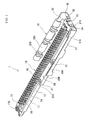
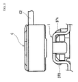
- Fig. 1 is a perspective view showing a whole configuration of the connector according to the embodiment
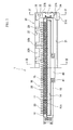
- Fig. 2 is a plan view thereof.
- a left half of a ground plate attached to the connector is omitted in the longitudinal direction.
- a connector 1 is formed to attach to a circuit board (not shown), and extends in left and right directions as shown in the figures.
- a ground plate 30 is selectively attached to a connector main body 10.
- a plurality of terminals 20 is arranged with a specific interval on an outer side surface 12 among the outer side surfaces 12 and 13 situated in a longitudinal direction of a housing 11 formed of an insulation material and elongated in the left and right directions.
- the housing 11 is provided with a fitting recess portion 14 opening upward and extending up to both ends in the longitudinal direction.
- the terminals 20 are arranged on one sidewall portion 15 extending in the longitudinal direction.
- the fitting recess portion 14 is situated at a center portion in a width direction, i.e., a direction perpendicular to the longitudinal direction.
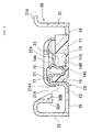
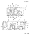
- Fig. 3 i.e., a sectional view taken along a line III-III in Fig. 2
- the fitting recess portion 14 is formed deep to an extent that a thin bottom wall 11A remains in the housing 11.
- the fitting recess portion 14 is provided with receptacle grooves 16 at positions corresponding to the terminals recessing from an inner side surface 14C of the one sidewall portion 15 over a vertical range from a position of an upper opening 14A to a bottom portion 14B or an upper surface of the bottom wall 11A.
- the receptacle grooves 16 have a depth deep enough for receiving almost the whole portion of elastic arms of the terminals (described later).
- Shallow grooves 17 communicating with the receptacle grooves 16 are formed in an upper end surface and an outer side surface of the sidewall portion 15.
- the terminals 20 to be attached to the housing 11 with the receptacle grooves 16 and the grooves 17 are formed of metal thin plates bent relative to a plate surface.
- a sectional shape taken along a plane perpendicular to the plate surface is a substantially S character shape.
- the terminal has continuously an inverted U character shape portion and a U character shape portion, thereby having a substantially S character shape as a whole.
- the terminal 20 has a fitting portion 21 having an inverted U character shape; an elastic arm portion 22 having a U character shape and connected thereto; and a connecting portion 23 extending from a lower end portion of the fitting portion 21.
- the fitting portion 21 is pressed and fitted into the receptacle groove 16 from above, so that the terminal 20 is fixed to the housing 11.
- the connecting portion 23 bent laterally and extending from the lower end of the fitting portion 21 outside the housing 11 is situated at a level same as that of a bottom surface of the housing 11. When the connector is installed on the circuit board, the connecting portion 23 contacts with the corresponding circuit portion of the circuit board.
- the elastic arm portion 22 is bent and extends upward from a lower portion of the fitting portion 21 fitted into the receptacle groove 16, and has elasticity with this flexible portion.
- the elastic arm portion 22 is provided at an upper end or a free end thereof with a contact portion 22A curved in a state protruded toward outside the receptacle groove 16.
- the contact portion 22A slightly protrudes from the inner side surface 14C toward inside the fitting recess portion 14.
- the terminal 20 slightly projects from an opening edge of the groove 17 at a portion thereof where the fitting portion 21 is retained in the groove 17 to form a sub-contact portion 21A.
- a projection 21A1 is formed for securing a contact with the mating connector and functioning as a lock.
- the housing 11 has ground plate attaching portions 11 B at both end portions thereof in the longitudinal direction.
- the ground plate 30 to be attached to the ground plate attaching portions 11B is formed of one metal plate punched and bent.
- the ground plate 30 has ground main portions 31 and 32 situated along the outer side surfaces 12 and 13 of the housing 11, and connecting members 34 and 35 for connecting the ground main portions 31 and 32 to an attaching portion 33.
- the connecting members 34 and 35 link lower portions of the attaching portions 33 to be attached to the ground plate attaching portions 11B and lower portions of the ground main portions 31 and 32, so that the connecting members 34 and 35 contact with the circuit board at both of the end portions of the housing 11 in the longitudinal direction.
- the connecting member 35 has an attaching hole 36.
- the ground main portion 31 has a surface substantially in parallel to the other outer side surface 13 of the housing 11 with a distance from the outer side surface 13. An upper edge of the ground main portion 31 is situated at a level same as that of an upper surface of the housing 11.
- the ground main portion 31 has curved projecting portions 31A projecting upward from the upper edge of the ground main portion 31 at only both of the end portions thereof in the longitudinal direction. Accordingly, when the mating connector is fitted, the upper edge of the ground main portion 31 does not interfere with a cable horizontally extending from the mating connector at a side of the ground main portion 31. That is, since the upper edge is situated at the position of the upper surface of the housing 11, the cable is allowed to extend at the upper position.
- a cut portion may be formed only at a position where the cable extends, and the upper edge may be extend upward, for example, the curved projecting portion may be formed over a whole range in the longitudinal direction except a position of the cut portion.
- the ground main portion 32 has a surface substantially in parallel to the outer side surface 12 of the housing 11 with a distance from the outer side surface 12. It is arranged such that the distance becomes greater than the distance in the case of the ground main portion 13.
- the connecting portions 23 of the terminals 20 are situated between the ground main portion 32 and the outer side surface 12 of the housing 11.
- the ground main portion 32 and the attaching portions 33 are connected with the connecting members 35 at both of the end portions in the longitudinal direction where the terminals are not disposed. Accordingly, the ground main portion 32 is apart from the attaching portions 33 to form a space in between, so that the connecting portions 23 are able to contact with the corresponding circuit portion of the circuit board.
- the ground main portion 32 has two types of curved portions 32A and 32B at an upper edge thereof curved toward inside (the housing side) and arranged alternately in the longitudinal direction.
- One of the curved portions 32A has a wide width
- the other of the curved portions 32B has a narrow width.
- the other of the curved portions 32B extends obliquely toward inside further than one of the curved portions 32A to form an elastic tongue piece.
- the elastic tongue piece forms a contact section for elastically contacting with a mating ground plate when fitted into the mating connector.
- the attaching portions 33 have an inverted U character shape to be fitted into the ground plate attaching portions 11B provided at both of the end portions of the housing 11. Outer surfaces of the attaching portions 33 function as portions where corresponding engaging portions of the mating connector are fitted into from above for engagement.
- the attaching portion 33 has lock portions on outer surface at both of the shoulder portions thereof.
- the lock portions are formed of projections, and include a main lock portion 37A situated at a side where the cable of the mating connector extends and a sub lock portion 37B situated at an opposite side.
- the main lock portion 37A projects for an amount greater than that of the sub lock portion 37B. That is, the main lock portion 37A engages the corresponding lock portion of the mating connector to a greater extent.
- a difference in the amount of projection is set in proportion of force received from the mating connector when the mating connector is detached by lifting the cable.
- the housing 11 has an absorption portion 40 at a center position in the longitudinal direction of the housing 11 on the side of the other outer side surface 13.
- the absorption portion 40 forms a portion to be absorbed by an absorption portion of an automated device when the automated device mounts the connector to a specific position on the circuit board.
- An upper surface 40A is flush with the upper surface of the housing and projects in the width direction of the housing.
- a side surface 40B of the projecting absorption portion 40 is close to the ground main portion 31.
- Attaching holes 41 are formed in the upper surface of the absorption portion 40 at both of the end positions in the longitudinal direction for attaching an auxiliary attaching member.
- the auxiliary attaching member is attached to the attaching holes 41 for enlarging an attaching surface. It is preferred that the absorption portion 40 is provided within a width of the mating connector.
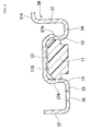
- Fig. 6 is a view showing a use state of the connector of the embodiment fitted into the mating connector, wherein Fig 6(A) shows a state in which the connector of the embodiment is used without the ground plate, and Fig 6(B) shows a state in which it is used with the ground plate.
- a mating connector C with a cable indicated by phantom lines has a coaxial cable C2 held between an insulation member and a part of the ground plate C 1 and extending laterally in the right direction.
- a center conductor C3 of the coaxial cable C2 is connected to a terminal C4.
- the terminal has an inverted U character shape portion and a U character shape to form a substantially S character shape as a whole.
- the ground plate C1 is attached to an outer side of the connector.
- the ground plate C1 covers an upper surface of the connector and an outer side surface except a side surface on a side where the cable extends.
- the mating connector C receives the terminal 20 of the connector of the embodiment inside the inverted U character shape portion of the terminal C4, and the U character shape portion enters the fitting recess portion 14 of the connector of the embodiment.
- the connector of the embodiment is used in the following manner.
- the absorption portion of the automated device absorbs the connector 1 at the absorption portion 40 (absorption surface 40A) of the connector 1, and moves the connector 1 to a specific position on the circuit board.
- the connecting portions 23 of the terminals are connected to the corresponding circuit portions of the circuit board with solder. It is possible to use the connector 1 in the state that the ground plate 30 is attached or in the state that there is no ground plate (only the portion where the ground plate of the mating connector is connected to the board). It is possible to attach the ground plate 30 before or after the connector is arranged on the circuit board. When the ground plate 30 is used, it is preferable to fix it with solder at the attaching holes 36 shown in Fig. 4 .
- the mating connector C is fitted into the connector 1.
- the terminals C4 of the mating connector C contact with the terminals 20 of the connector 1 while surrounding in the inverted U character shape portion. That is, one of straight portions of the inverted U character shape portion of the terminal C4 contacts with the sub contact portion 21 A of the terminal 20 of the connector 1, and an opposite straight portion elastically presses the contact portion 22A.
- the contact portion 22A is pushed into the receptacle groove 16.
- the U character shape portion of the terminal C4 of the mating connector enters up to a bottom portion of the fitting recess portion 14.
- the U character shape portion of the terminal C4 enters downward up to a position substantially same as the elastic arm portion 22 of the terminal of the connector 1.
- the straight portion contacting with the contact portion 22A has a long contact length during the fitting process, and it is possible to minimize heights of both of the connectors upon fitting.
- the ground main portions 31 and 32 cover the connector 1 sideways over a large range extending in the longitudinal direction of the connector 1.
- the ground plate C1 of the mating connector C covers the upper portion of both of the connectors C and 1.
- the contact sections 32B formed as the elastic tongue pieces contact with the ground plate C1 of the mating connector C, thereby mutually conducting at the positions.
- the cable C2 extending from the mating connector C is drawn through above the upper edge of the ground main portion 31 without interference with the ground plate.
- the lock portions engage the lock portions 37A and 37B with the projecting shape, so that the connectors are not separated inadvertently.
- the lock portion 37A close to the cable C2 receives a force larger than that of the opposite lock portion 37B as shown in Fig. 5 .
- the lock portion 37A engages to a larger extent than the lock portion 37B, it is possible to properly prevent the connector from coming off according to the balance of forces.
- the lock portions 37A and 37B are provided at both of the end portions of the ground plate 30 in the longitudinal direction, and may be provided on the housing 11. It is preferred that the lock portion of the mating connector is provided on the mating ground plate, so that the lock portion contacts to the lock portions 37A and 37B provided on the ground plate 30.
- the electric connector to be attached to a circuit board according to the present invention can be used in an electric device which requires minimizing a height on the circuit board when mounted to the circuit board.
Landscapes
- Details Of Connecting Devices For Male And Female Coupling (AREA)
- Coupling Device And Connection With Printed Circuit (AREA)
Applications Claiming Priority (2)
| Application Number | Priority Date | Filing Date | Title |
|---|---|---|---|
| JP2005307086A JP4349633B2 (ja) | 2005-10-21 | 2005-10-21 | 回路基板用電気コネクタ |
| PCT/JP2006/320901 WO2007046488A1 (ja) | 2005-10-21 | 2006-10-20 | 回路基板用電気コネクタ |
Publications (1)
| Publication Number | Publication Date |
|---|---|
| EP1950845A1 true EP1950845A1 (en) | 2008-07-30 |
Family
ID=37950734
Family Applications (1)
| Application Number | Title | Priority Date | Filing Date |
|---|---|---|---|
| EP06812069A Withdrawn EP1950845A1 (en) | 2005-10-21 | 2006-10-20 | Electric connector for circuit board |
Country Status (7)
| Country | Link |
|---|---|
| US (1) | US7207842B1 (enExample) |
| EP (1) | EP1950845A1 (enExample) |
| JP (1) | JP4349633B2 (enExample) |
| KR (1) | KR20070043653A (enExample) |
| CN (1) | CN100511868C (enExample) |
| TW (1) | TW200717931A (enExample) |
| WO (1) | WO2007046488A1 (enExample) |
Families Citing this family (26)
| Publication number | Priority date | Publication date | Assignee | Title |
|---|---|---|---|---|
| JP4563915B2 (ja) * | 2005-10-21 | 2010-10-20 | ヒロセ電機株式会社 | 回路基板用電気コネクタ |
| TWD121455S1 (zh) * | 2006-09-12 | 2008-02-21 | 星電股份有限公司 | 連接器 |
| JP4978313B2 (ja) * | 2007-05-31 | 2012-07-18 | オムロン株式会社 | コネクタ |
| CN201060991Y (zh) * | 2007-06-11 | 2008-05-14 | 江苏华富电子有限公司 | 板对板电连接器 |
| JP4522440B2 (ja) * | 2007-07-26 | 2010-08-11 | 日本航空電子工業株式会社 | 基板搭載用コネクタ及びその相手方コネクタ並びにそれらを備えた電子機器 |
| JP4691738B2 (ja) * | 2008-09-01 | 2011-06-01 | ヒロセ電機株式会社 | シールド機能を有するコネクタ装置 |
| TWI394327B (zh) * | 2008-09-16 | 2013-04-21 | Hon Hai Prec Ind Co Ltd | 電連接器 |
| US20100093210A1 (en) * | 2008-10-10 | 2010-04-15 | Kunshan Jiahua Electronics Co., Ltd. | Coaxial electrical connector |
| TWI398993B (zh) * | 2009-03-09 | 2013-06-11 | Hon Hai Prec Ind Co Ltd | 電連接器組件 |
| JP5426470B2 (ja) * | 2010-05-11 | 2014-02-26 | 株式会社アドバンテスト | コネクタ及びそれを有する半導体試験装置 |
| US8888506B2 (en) * | 2013-01-29 | 2014-11-18 | Japan Aviation Electronics Industry, Limited | Connector |
| US9112302B2 (en) * | 2013-05-02 | 2015-08-18 | Hon Hai Precision Industry Co., Ltd. | Electrical connector and assembly thereof |
| JP6249676B2 (ja) * | 2013-08-21 | 2017-12-20 | 宏致電子股▲ふん▼有限公司Aces Electronics Co.,Ltd. | 電気コネクタ |
| JP5887326B2 (ja) * | 2013-12-12 | 2016-03-16 | モレックス エルエルシー | コネクタ |
| JP6269558B2 (ja) * | 2014-06-05 | 2018-01-31 | 株式会社村田製作所 | コネクタセット及びコネクタ |
| JP6436350B2 (ja) * | 2015-03-18 | 2018-12-12 | 第一精工株式会社 | コネクタ装置 |
| JP6593118B2 (ja) * | 2015-11-13 | 2019-10-23 | 住友電装株式会社 | 基板用コネクタ及び基板用コネクタの製造方法 |
| JP6826773B2 (ja) * | 2016-09-16 | 2021-02-10 | I−Pex株式会社 | ケーブル用電気コネクタ装置 |
| CN107394538A (zh) * | 2017-06-12 | 2017-11-24 | 深圳市长盈精密技术股份有限公司 | 大电流板对板插头、插座及连接器组件 |
| JP6690665B2 (ja) * | 2018-05-10 | 2020-04-28 | 第一精工株式会社 | 基板コネクタ装置 |
| JP6714056B2 (ja) * | 2018-09-12 | 2020-06-24 | モレックス エルエルシー | コネクタ |
| US10594074B1 (en) * | 2018-10-30 | 2020-03-17 | Microsoft Technology Licensing, Llc | Shielded magnetic electronic connector |
| JP6859998B2 (ja) | 2018-12-28 | 2021-04-14 | I−Pex株式会社 | 電気コネクタおよびコネクタ装置 |
| JP7245052B2 (ja) * | 2019-01-07 | 2023-03-23 | ヒロセ電機株式会社 | コネクタ及びコネクタ装置 |
| JP7439608B2 (ja) * | 2020-03-26 | 2024-02-28 | 株式会社オートネットワーク技術研究所 | カードエッジコネクタ及び回路基板 |
| JP7467234B2 (ja) * | 2020-05-28 | 2024-04-15 | 日本航空電子工業株式会社 | フローティングコネクタ |
Family Cites Families (7)
| Publication number | Priority date | Publication date | Assignee | Title |
|---|---|---|---|---|
| JPH0546230Y2 (enExample) * | 1990-02-27 | 1993-12-02 | ||
| TW330737U (en) * | 1997-06-05 | 1998-04-21 | Hon Hai Prec Ind Co Ltd | Connector for high density plugs |
| JP3654493B2 (ja) * | 1999-03-16 | 2005-06-02 | タイコエレクトロニクスアンプ株式会社 | フレキシブル回路基板の接続構造 |
| JP4324822B2 (ja) | 1999-05-21 | 2009-09-02 | 株式会社アイペックス | ケーブル用コネクタ |
| JP2002008753A (ja) * | 2000-06-16 | 2002-01-11 | Matsushita Electric Works Ltd | コネクタ |
| US6645005B2 (en) * | 2001-11-29 | 2003-11-11 | Hon Hai Precision Ind. Co., Ltd. | Electrical connector assembly with latching metal ears |
| JP3963758B2 (ja) * | 2002-03-29 | 2007-08-22 | 本多通信工業株式会社 | 同軸コネクタ |
-
2005
- 2005-10-21 JP JP2005307086A patent/JP4349633B2/ja not_active Expired - Fee Related
-
2006
- 2006-10-18 TW TW095138402A patent/TW200717931A/zh not_active IP Right Cessation
- 2006-10-19 US US11/582,998 patent/US7207842B1/en not_active Expired - Fee Related
- 2006-10-20 KR KR1020060102182A patent/KR20070043653A/ko not_active Withdrawn
- 2006-10-20 WO PCT/JP2006/320901 patent/WO2007046488A1/ja not_active Ceased
- 2006-10-20 EP EP06812069A patent/EP1950845A1/en not_active Withdrawn
- 2006-10-23 CN CNB200610136579XA patent/CN100511868C/zh not_active Expired - Fee Related
Non-Patent Citations (1)
| Title |
|---|
| See references of WO2007046488A1 * |
Also Published As
| Publication number | Publication date |
|---|---|
| JP2007115575A (ja) | 2007-05-10 |
| US20070093085A1 (en) | 2007-04-26 |
| CN1967948A (zh) | 2007-05-23 |
| JP4349633B2 (ja) | 2009-10-21 |
| US7207842B1 (en) | 2007-04-24 |
| CN100511868C (zh) | 2009-07-08 |
| WO2007046488A1 (ja) | 2007-04-26 |
| TWI329943B (enExample) | 2010-09-01 |
| KR20070043653A (ko) | 2007-04-25 |
| TW200717931A (en) | 2007-05-01 |
Similar Documents
| Publication | Publication Date | Title |
|---|---|---|
| EP1950845A1 (en) | Electric connector for circuit board | |
| EP3696921B1 (en) | Connector | |
| US9401570B2 (en) | Electrical connector having ground bus bar | |
| US9466930B2 (en) | Flippable electrical connector | |
| US7448897B2 (en) | Plug connector with mating protection | |
| US9196984B2 (en) | Substrate connection structure using substrate connector | |
| CN214849145U (zh) | 连接器 | |
| US20080038963A1 (en) | Receptacle connector and apparatus having the same | |
| US7134900B2 (en) | Electrical connector assembly with multi-function latching member | |
| US6629859B2 (en) | Shielded connector assembly | |
| US6814605B2 (en) | Connector having a shielding shell provided with a locking portion | |
| US11177601B2 (en) | Terminal having a conductor and a spring | |
| US6604964B2 (en) | Shielded connector assembly | |
| US7607943B2 (en) | Electric connector for circuit board | |
| US6056600A (en) | Shielded connector | |
| US7056133B2 (en) | Surface mounting connector | |
| US8851922B2 (en) | Electrical connector device and connector used in the electrical connector device | |
| JP2007115579A (ja) | 回路基板用電気コネクタ | |
| CN220797279U (zh) | 电连接器及连接器组件 | |
| JP2007115578A (ja) | 回路基板用電気コネクタ | |
| JP4552343B2 (ja) | コンタクト部品および該コンタクト部品を備えたコネクタ | |
| JP2025162126A (ja) | 回路基板用電気コネクタ | |
| JPH0773932A (ja) | プラグ組立体及びコネクタ | |
| JP2002298992A (ja) | コネクタ | |
| JP2002298988A (ja) | コネクタ |
Legal Events
| Date | Code | Title | Description |
|---|---|---|---|
| PUAI | Public reference made under article 153(3) epc to a published international application that has entered the european phase |
Free format text: ORIGINAL CODE: 0009012 |
|
| 17P | Request for examination filed |
Effective date: 20080521 |
|
| AK | Designated contracting states |
Kind code of ref document: A1 Designated state(s): DE FI FR GB IT |
|
| DAX | Request for extension of the european patent (deleted) | ||
| RBV | Designated contracting states (corrected) |
Designated state(s): DE FI FR GB IT |
|
| STAA | Information on the status of an ep patent application or granted ep patent |
Free format text: STATUS: THE APPLICATION HAS BEEN WITHDRAWN |
|
| 18W | Application withdrawn |
Effective date: 20100830 |