US9196984B2 - Substrate connection structure using substrate connector - Google Patents

Substrate connection structure using substrate connector Download PDF

Info

Publication number
US9196984B2
US9196984B2 US14/159,385 US201414159385A US9196984B2 US 9196984 B2 US9196984 B2 US 9196984B2 US 201414159385 A US201414159385 A US 201414159385A US 9196984 B2 US9196984 B2 US 9196984B2
Authority
US
United States
Prior art keywords
plug
guide
substrate
socket
face
Prior art date
Legal status (The legal status is an assumption and is not a legal conclusion. Google has not performed a legal analysis and makes no representation as to the accuracy of the status listed.)
Expired - Fee Related, expires
Application number
US14/159,385
Other versions
US20140315419A1 (en
Inventor
Yoshiyasu ISHIDA
Fumio Ohsawa
Kiyoshi Asai
Current Assignee (The listed assignees may be inaccurate. Google has not performed a legal analysis and makes no representation or warranty as to the accuracy of the list.)
SMK Corp
Original Assignee
SMK Corp
Priority date (The priority date is an assumption and is not a legal conclusion. Google has not performed a legal analysis and makes no representation as to the accuracy of the date listed.)
Filing date
Publication date
Application filed by SMK Corp filed Critical SMK Corp
Assigned to SMK CORPORATION reassignment SMK CORPORATION ASSIGNMENT OF ASSIGNORS INTEREST (SEE DOCUMENT FOR DETAILS). Assignors: ASAI, KIYOSHI, ISHIDA, YOSHIYASU, OHSAWA, FUMIO
Publication of US20140315419A1 publication Critical patent/US20140315419A1/en
Application granted granted Critical
Publication of US9196984B2 publication Critical patent/US9196984B2/en
Expired - Fee Related legal-status Critical Current
Adjusted expiration legal-status Critical

Links

Images

Classifications

    • HELECTRICITY
    • H01ELECTRIC ELEMENTS
    • H01RELECTRICALLY-CONDUCTIVE CONNECTIONS; STRUCTURAL ASSOCIATIONS OF A PLURALITY OF MUTUALLY-INSULATED ELECTRICAL CONNECTING ELEMENTS; COUPLING DEVICES; CURRENT COLLECTORS
    • H01R12/00Structural associations of a plurality of mutually-insulated electrical connecting elements, specially adapted for printed circuits, e.g. printed circuit boards [PCB], flat or ribbon cables, or like generally planar structures, e.g. terminal strips, terminal blocks; Coupling devices specially adapted for printed circuits, flat or ribbon cables, or like generally planar structures; Terminals specially adapted for contact with, or insertion into, printed circuits, flat or ribbon cables, or like generally planar structures
    • H01R12/70Coupling devices
    • H01R12/71Coupling devices for rigid printing circuits or like structures
    • H01R12/712Coupling devices for rigid printing circuits or like structures co-operating with the surface of the printed circuit or with a coupling device exclusively provided on the surface of the printed circuit
    • H01R12/716Coupling device provided on the PCB
    • HELECTRICITY
    • H01ELECTRIC ELEMENTS
    • H01RELECTRICALLY-CONDUCTIVE CONNECTIONS; STRUCTURAL ASSOCIATIONS OF A PLURALITY OF MUTUALLY-INSULATED ELECTRICAL CONNECTING ELEMENTS; COUPLING DEVICES; CURRENT COLLECTORS
    • H01R12/00Structural associations of a plurality of mutually-insulated electrical connecting elements, specially adapted for printed circuits, e.g. printed circuit boards [PCB], flat or ribbon cables, or like generally planar structures, e.g. terminal strips, terminal blocks; Coupling devices specially adapted for printed circuits, flat or ribbon cables, or like generally planar structures; Terminals specially adapted for contact with, or insertion into, printed circuits, flat or ribbon cables, or like generally planar structures
    • H01R12/70Coupling devices
    • H01R12/7005Guiding, mounting, polarizing or locking means; Extractors
    • H01R12/7011Locking or fixing a connector to a PCB
    • H01R12/7052Locking or fixing a connector to a PCB characterised by the locating members
    • HELECTRICITY
    • H01ELECTRIC ELEMENTS
    • H01RELECTRICALLY-CONDUCTIVE CONNECTIONS; STRUCTURAL ASSOCIATIONS OF A PLURALITY OF MUTUALLY-INSULATED ELECTRICAL CONNECTING ELEMENTS; COUPLING DEVICES; CURRENT COLLECTORS
    • H01R12/00Structural associations of a plurality of mutually-insulated electrical connecting elements, specially adapted for printed circuits, e.g. printed circuit boards [PCB], flat or ribbon cables, or like generally planar structures, e.g. terminal strips, terminal blocks; Coupling devices specially adapted for printed circuits, flat or ribbon cables, or like generally planar structures; Terminals specially adapted for contact with, or insertion into, printed circuits, flat or ribbon cables, or like generally planar structures
    • H01R12/70Coupling devices
    • H01R12/71Coupling devices for rigid printing circuits or like structures
    • H01R12/712Coupling devices for rigid printing circuits or like structures co-operating with the surface of the printed circuit or with a coupling device exclusively provided on the surface of the printed circuit
    • H01R12/714Coupling devices for rigid printing circuits or like structures co-operating with the surface of the printed circuit or with a coupling device exclusively provided on the surface of the printed circuit with contacts abutting directly the printed circuit; Button contacts therefore provided on the printed circuit
    • HELECTRICITY
    • H01ELECTRIC ELEMENTS
    • H01RELECTRICALLY-CONDUCTIVE CONNECTIONS; STRUCTURAL ASSOCIATIONS OF A PLURALITY OF MUTUALLY-INSULATED ELECTRICAL CONNECTING ELEMENTS; COUPLING DEVICES; CURRENT COLLECTORS
    • H01R12/00Structural associations of a plurality of mutually-insulated electrical connecting elements, specially adapted for printed circuits, e.g. printed circuit boards [PCB], flat or ribbon cables, or like generally planar structures, e.g. terminal strips, terminal blocks; Coupling devices specially adapted for printed circuits, flat or ribbon cables, or like generally planar structures; Terminals specially adapted for contact with, or insertion into, printed circuits, flat or ribbon cables, or like generally planar structures
    • H01R12/70Coupling devices
    • H01R12/71Coupling devices for rigid printing circuits or like structures
    • H01R12/72Coupling devices for rigid printing circuits or like structures coupling with the edge of the rigid printed circuits or like structures
    • H01R12/722Coupling devices for rigid printing circuits or like structures coupling with the edge of the rigid printed circuits or like structures coupling devices mounted on the edge of the printed circuits
    • H01R12/727Coupling devices presenting arrays of contacts
    • HELECTRICITY
    • H01ELECTRIC ELEMENTS
    • H01RELECTRICALLY-CONDUCTIVE CONNECTIONS; STRUCTURAL ASSOCIATIONS OF A PLURALITY OF MUTUALLY-INSULATED ELECTRICAL CONNECTING ELEMENTS; COUPLING DEVICES; CURRENT COLLECTORS
    • H01R12/00Structural associations of a plurality of mutually-insulated electrical connecting elements, specially adapted for printed circuits, e.g. printed circuit boards [PCB], flat or ribbon cables, or like generally planar structures, e.g. terminal strips, terminal blocks; Coupling devices specially adapted for printed circuits, flat or ribbon cables, or like generally planar structures; Terminals specially adapted for contact with, or insertion into, printed circuits, flat or ribbon cables, or like generally planar structures
    • H01R12/70Coupling devices
    • H01R12/91Coupling devices allowing relative movement between coupling parts, e.g. floating or self aligning
    • HELECTRICITY
    • H01ELECTRIC ELEMENTS
    • H01RELECTRICALLY-CONDUCTIVE CONNECTIONS; STRUCTURAL ASSOCIATIONS OF A PLURALITY OF MUTUALLY-INSULATED ELECTRICAL CONNECTING ELEMENTS; COUPLING DEVICES; CURRENT COLLECTORS
    • H01R13/00Details of coupling devices of the kinds covered by groups H01R12/70 or H01R24/00 - H01R33/00
    • H01R13/62Means for facilitating engagement or disengagement of coupling parts or for holding them in engagement
    • H01R13/629Additional means for facilitating engagement or disengagement of coupling parts, e.g. aligning or guiding means, levers, gas pressure electrical locking indicators, manufacturing tolerances
    • H01R13/631Additional means for facilitating engagement or disengagement of coupling parts, e.g. aligning or guiding means, levers, gas pressure electrical locking indicators, manufacturing tolerances for engagement only
    • H01R13/6315Additional means for facilitating engagement or disengagement of coupling parts, e.g. aligning or guiding means, levers, gas pressure electrical locking indicators, manufacturing tolerances for engagement only allowing relative movement between coupling parts, e.g. floating connection
    • HELECTRICITY
    • H01ELECTRIC ELEMENTS
    • H01RELECTRICALLY-CONDUCTIVE CONNECTIONS; STRUCTURAL ASSOCIATIONS OF A PLURALITY OF MUTUALLY-INSULATED ELECTRICAL CONNECTING ELEMENTS; COUPLING DEVICES; CURRENT COLLECTORS
    • H01R12/00Structural associations of a plurality of mutually-insulated electrical connecting elements, specially adapted for printed circuits, e.g. printed circuit boards [PCB], flat or ribbon cables, or like generally planar structures, e.g. terminal strips, terminal blocks; Coupling devices specially adapted for printed circuits, flat or ribbon cables, or like generally planar structures; Terminals specially adapted for contact with, or insertion into, printed circuits, flat or ribbon cables, or like generally planar structures
    • H01R12/50Fixed connections
    • H01R12/51Fixed connections for rigid printed circuits or like structures
    • H01R12/55Fixed connections for rigid printed circuits or like structures characterised by the terminals
    • H01R12/57Fixed connections for rigid printed circuits or like structures characterised by the terminals surface mounting terminals
    • HELECTRICITY
    • H01ELECTRIC ELEMENTS
    • H01RELECTRICALLY-CONDUCTIVE CONNECTIONS; STRUCTURAL ASSOCIATIONS OF A PLURALITY OF MUTUALLY-INSULATED ELECTRICAL CONNECTING ELEMENTS; COUPLING DEVICES; CURRENT COLLECTORS
    • H01R12/00Structural associations of a plurality of mutually-insulated electrical connecting elements, specially adapted for printed circuits, e.g. printed circuit boards [PCB], flat or ribbon cables, or like generally planar structures, e.g. terminal strips, terminal blocks; Coupling devices specially adapted for printed circuits, flat or ribbon cables, or like generally planar structures; Terminals specially adapted for contact with, or insertion into, printed circuits, flat or ribbon cables, or like generally planar structures
    • H01R12/70Coupling devices
    • H01R12/71Coupling devices for rigid printing circuits or like structures
    • H01R12/72Coupling devices for rigid printing circuits or like structures coupling with the edge of the rigid printed circuits or like structures
    • H01R12/73Coupling devices for rigid printing circuits or like structures coupling with the edge of the rigid printed circuits or like structures connecting to other rigid printed circuits or like structures
    • HELECTRICITY
    • H01ELECTRIC ELEMENTS
    • H01RELECTRICALLY-CONDUCTIVE CONNECTIONS; STRUCTURAL ASSOCIATIONS OF A PLURALITY OF MUTUALLY-INSULATED ELECTRICAL CONNECTING ELEMENTS; COUPLING DEVICES; CURRENT COLLECTORS
    • H01R13/00Details of coupling devices of the kinds covered by groups H01R12/70 or H01R24/00 - H01R33/00
    • H01R13/02Contact members
    • H01R13/20Pins, blades, or sockets shaped, or provided with separate member, to retain co-operating parts together
    • HELECTRICITY
    • H01ELECTRIC ELEMENTS
    • H01RELECTRICALLY-CONDUCTIVE CONNECTIONS; STRUCTURAL ASSOCIATIONS OF A PLURALITY OF MUTUALLY-INSULATED ELECTRICAL CONNECTING ELEMENTS; COUPLING DEVICES; CURRENT COLLECTORS
    • H01R13/00Details of coupling devices of the kinds covered by groups H01R12/70 or H01R24/00 - H01R33/00
    • H01R13/62Means for facilitating engagement or disengagement of coupling parts or for holding them in engagement
    • H01R13/627Snap or like fastening
    • H01R13/6271Latching means integral with the housing
    • H01R13/6272Latching means integral with the housing comprising a single latching arm
    • HELECTRICITY
    • H01ELECTRIC ELEMENTS
    • H01RELECTRICALLY-CONDUCTIVE CONNECTIONS; STRUCTURAL ASSOCIATIONS OF A PLURALITY OF MUTUALLY-INSULATED ELECTRICAL CONNECTING ELEMENTS; COUPLING DEVICES; CURRENT COLLECTORS
    • H01R13/00Details of coupling devices of the kinds covered by groups H01R12/70 or H01R24/00 - H01R33/00
    • H01R13/62Means for facilitating engagement or disengagement of coupling parts or for holding them in engagement
    • H01R13/629Additional means for facilitating engagement or disengagement of coupling parts, e.g. aligning or guiding means, levers, gas pressure electrical locking indicators, manufacturing tolerances
    • H01R13/631Additional means for facilitating engagement or disengagement of coupling parts, e.g. aligning or guiding means, levers, gas pressure electrical locking indicators, manufacturing tolerances for engagement only
    • HELECTRICITY
    • H01ELECTRIC ELEMENTS
    • H01RELECTRICALLY-CONDUCTIVE CONNECTIONS; STRUCTURAL ASSOCIATIONS OF A PLURALITY OF MUTUALLY-INSULATED ELECTRICAL CONNECTING ELEMENTS; COUPLING DEVICES; CURRENT COLLECTORS
    • H01R13/00Details of coupling devices of the kinds covered by groups H01R12/70 or H01R24/00 - H01R33/00
    • H01R13/62Means for facilitating engagement or disengagement of coupling parts or for holding them in engagement
    • H01R13/639Additional means for holding or locking coupling parts together, after engagement, e.g. separate keylock, retainer strap
    • HELECTRICITY
    • H01ELECTRIC ELEMENTS
    • H01RELECTRICALLY-CONDUCTIVE CONNECTIONS; STRUCTURAL ASSOCIATIONS OF A PLURALITY OF MUTUALLY-INSULATED ELECTRICAL CONNECTING ELEMENTS; COUPLING DEVICES; CURRENT COLLECTORS
    • H01R13/00Details of coupling devices of the kinds covered by groups H01R12/70 or H01R24/00 - H01R33/00
    • H01R13/64Means for preventing incorrect coupling
    • H01R13/641Means for preventing incorrect coupling by indicating incorrect coupling; by indicating correct or full engagement
    • H01R23/725
    • H01R9/096

Definitions

  • a substrate connector including: a plug having a plug portion of an elongated and protruded shape with a plurality of plug-side signal terminals arranged along an outer side surface thereof; and a socket having a plug insertion groove into which the plug portion is to be inserted and a plurality of socket-side signal terminals arranged along an inner side surface of the plug insertion groove has been conventionally employed in order to electrically connect substrates. Electrical connection is achieved by connecting the plug to the socket in such a manner that the plug portion is fitted into the plug insertion groove and the above-described both signal terminals are resiliently brought into contact with each other.
  • Such a substrate connector includes: guiding portions provided at opposite ends of the socket in the longitudinal direction and each having a rectangular guide groove directed in a connection direction; and cuboid guided portions provided at opposite ends of the plug in the longitudinal direction.
  • a side surface of the guided portion in the width direction and an end face thereof in the longitudinal direction are guided by an inner side surface of the guide groove, thereby enabling the plug portion to be fitted into the plug insertion groove at a predetermined position (see Patent Literature 1, for example).
  • the substrate connector also includes a guide face formed at an edge portion of an opening in the guide groove by a slant surface slanted downwardly toward the inner side. If a relative position between the socket and the plug is misaligned in the horizontal direction during a connecting operation thereof, a slant surface formed at a side edge or end of the guided portion is slid over the guide face, thereby leading the guided portion to the guide groove. It is therefore possible to absorb such misalignment.
  • an escape hole in communication with the guide groove and passing completely through the mate-side substrate mounting surface, is provided in the guiding portion and the guide protrusion provided in the guided portion protrudes farther beyond the mate-side substrate mounting surface through the escape hole in addition to the configuration according to the first aspect.
  • an escape cutout portion having a hole shape or a cutout shape for the guide protrusion to be inserted therein is provided in the substrate in addition to the configuration according to the first or second aspect.
  • a substrate connection structure using a substrate connector employs a substrate connector including a plug and a socket to be mounted on substrates, respectively, and fitted together.
  • One of the plug and the socket includes a guiding portion having a guide groove directed in a connection direction
  • the other of the plug and the socket includes a guided portion to be fitted into the guide groove.
  • the guided portion is guided by an inner side surface of the guide groove, thereby enabling the plug to be fitted into the socket at a predetermined position.
  • a guide protrusion is provided at a mate-side end face of the guided portion and/or the guiding portion so as to protrude farther beyond a mate-side substrate mounting surface when the plug is fitted into the socket.
  • a first-side guide face is formed in the guided portion or an edge portion of an opening in the guide groove and the guide protrusion is provided with a second-side guide face slidable with the first-side guide face so as to lead the guided portion into the guide groove. Also, interference between the guide protrusion and the mate-side substrate is prevented from occurring. It is therefore possible to ensure a sufficient distance for adjusting positional misalignment while achieving a reduction in size and height of the overall connector. It is further possible to promote efficiency in the connecting operation.
  • an escape hole in communication with the guide groove and passing completely through the mate-side substrate mounting surface, is provided in the guiding portion and the guide protrusion provided in the guided portion protrudes farther beyond the mate-side substrate mounting surface through the escape hole.
  • the guide protrusion can be provided in the guided portion and it is possible to ensure a sufficient distance for adjusting positional misalignment while achieving a reduction in size and height of the overall connector.
  • FIG. 1A is a plan view illustrating an example of a substrate connection structure using a substrate connector according to the present invention
  • FIG. 1B is an elevation view of the same
  • FIG. 1C is a side view of the same.
  • FIG. 3 is a perspective view illustrating the substrate connector of FIGS. 1A to 1C .
  • FIG. 4 is a perspective view illustrating the same substrate connector as viewed from another direction.
  • FIG. 5A is a plan view illustrating a plug of FIGS. 1A to 1C
  • FIG. 5B is an elevation view of the same
  • FIG. 5C is a side view of the same.
  • FIG. 7 is a bottom view illustrating an example of the substrate of FIGS. 1A to 1C .
  • FIGS. 8A , 8 B, and 8 C are each a partial enlarged cross-sectional view for illustrating the operation of adjusting positional misalignment in the longitudinal direction of the connector.
  • FIGS. 9A , 9 B, 9 C, and 9 D are each a partial enlarged cross-sectional view for illustrating the operation of adjusting positional misalignment in the width direction of the same connector.
  • FIG. 11 is a partial enlarged cross-sectional view taken along line D-D of FIG. 10A .
  • FIG. 12 is a perspective view illustrating the substrate connector of FIGS. 10A to 10C .
  • FIG. 13 is a perspective view illustrating the same substrate connector as viewed in another direction.
  • FIG. 14A is a plan view illustrating a plug of FIGS. 10A to 10C
  • FIG. 14B is an elevation view of the same
  • FIG. 14C is a side view of the same.
  • FIG. 15A is a plan view illustrating a socket of FIGS. 10A to 10C
  • FIG. 15B is an elevation view of the same
  • FIG. 15C is a cross-sectional view taken along line F-F of FIG. 15B
  • FIG. 15D is a cross-sectional view taken along line E-E of FIG. 15A .
  • FIGS. 17A , 17 B, and 17 C are each a partial enlarged cross-sectional view for illustrating the operation of adjusting positional misalignment in the width direction of the same connector.
  • FIGS. 1 to 9D A first embodiment of a substrate connection structure using a substrate connector according to the present invention will now be described based on examples illustrated in FIGS. 1 to 9D .
  • reference numerals b 1 and b 2 denote substrates, respectively.
  • the substrate b 1 may be a PCB
  • the substrate b 2 may be an FPC, for example.
  • the substrate connector 1 includes a plug 4 and a socket 7 .
  • the plug 4 has plug portions 3 each having an elongated and protruded shape.
  • the plug portion 3 includes a plurality of plug-side signal terminals 2 arranged along a lateral portion thereof.
  • the socket 7 includes a plurality of socket-side signal terminals 6 arranged along inner side surface portions of plug insertion grooves 5 into which the plug portions 3 are to be inserted. Fitting the plug portions 3 into the plug insertion grooves 5 achieves the connection between the plug-side signal terminals 2 and the socket-side signal terminals 6 .
  • the substrates b 1 and b 2 with the plug 4 and the socket 7 mounted thereon, respectively are electrically connected to each other via these signal terminals 2 and 6 .
  • a longitudinal direction of the plug portion 3 being referred to as a longitudinal direction, a horizontal direction perpendicular to the longitudinal direction as a width direction, and a direction in which the plug 4 and the socket 7 face each other as a connection direction.
  • the socket 7 is provided with guiding portions 9 , each having a guide groove 8 directed in the connection direction, and the plug 4 is provided with guided portions 10 to be fitted into the guide grooves 8 .
  • the guided portion 10 is guided by an inner side surface of the guide groove 8 , thereby enabling the plug portions 3 to be fitted into the respective plug insertion grooves 5 at predetermined positions.
  • the plug main body 11 is integrally formed with an insulating synthetic resin.
  • the plug main body 11 includes: a main body base 12 of a flat-plate shape; the plug portions 3 each having an elongated and protruded shape, protruded from a surface of the main body base 12 and extending in the longitudinal direction; and the guided portions 10 disposed at opposite ends thereof in the longitudinal direction.
  • the main body base 12 and the plug portions 3 together form a shape such that U-shaped cross sections continuously appear in the longitudinal direction.
  • the plug portions 3 and the guided portions 10 disposed at the opposite ends thereof together form a rectangular frame shape as viewed from above.
  • the guided portion 10 is formed in a cuboid shape.
  • the guided portion 10 integrally has a guide slant portion 13 , having a shape bulging toward the socket 7 (the mate side thereof), on a socket-side end face thereof.
  • the guide slant portion 13 is formed in such a manner that a height of the socket-side end face thereof is greater than that of the plug portions 3 .
  • the guide slant portion 13 also has a shape of a truncated square pyramid with guide slant faces 13 a formed along a peripheral portion thereof.
  • a guide protrusion 14 is provided on the mate-side end face of the guided portion 10 so as to protrude toward the socket 7 side in the connection direction.
  • the guide protrusion 14 is formed by integrating, by means of insert molding, a plug hold-down member 16 made of a metal plate material with a surface portion of a protrusion base 15 made of an insulating synthetic resin and integrally formed with the guided portion 10 .
  • the guide protrusion 14 and the guided portion 10 together form a protruding shape as viewed from the end face thereof in the longitudinal direction.
  • the plug hold-down member 16 is obtained by bending a conductive metal plate material having a strip shape to be formed in an inverted U-shape with an arc-like top thereof facing upward.
  • the plug hold-down member 16 is integrated with the surface portion of the protrusion base 15 with the outer surface thereof being exposed.
  • the longitudinal-direction guide face 17 is formed by a surface portion of the plug hold-down member 16 so as to have an arc-like cross section bulging upwardly.
  • the upper end of the protrusion base 15 has slant faces 18 formed along opposite edges thereof in the width direction.
  • the slant faces 18 are slanted toward an inner side in the connection direction.
  • the slant faces 18 form second-side (the guided portion side) width-direction guide faces slidable with first-side (the guiding portion side) width-direction guide faces to be described later.
  • a top position of the guide protrusion 14 i.e., a length in the connection direction extending from a substrate mounting surface 4 a of the plug 4 to the apex of the guide protrusion 14 , is set to be greater than the overall height of the socket 7 .
  • the guide protrusion 14 is configured such that it protrudes toward the substrate b 2 beyond a mate-side substrate mounting surface 7 a , i.e., the lower surface 7 a of the socket 7 when the plug 4 is fitted into the socket 7 .
  • the socket 7 includes: a socket main body 20 made of an insulating resin material; the plurality of socket-side signal terminals 6 ; and socket hold-down members 21 made of a conductive metal material as illustrated in FIGS. 6A to 6D .
  • the socket 7 is formed by integrating the socket-side signal terminals 6 and the socket hold-down members 21 with the socket main body 20 .
  • the guiding portions 9 are disposed at opposite ends of a fitting portion 22 of a flat-plate shape.
  • the guiding portions 9 are formed by integrating the socket hold-down members 21 made of a conductive metal plate material with the opposite ends of the socket main body 20 .
  • the guiding portions 9 are provided so as to be continuous with the side walls 24 of the fitting portion 22 .
  • the guiding portion 9 includes: peripheral walls 26 faced each other in the width direction; and an end wall 27 disposed at an end portion in the longitudinal direction.
  • the guide groove 8 directed in the connection direction is formed by being surrounded by the peripheral walls 26 , the end wall 27 , and an end face of the fitting portion 22 .
  • the end wall 27 has a first-side (the guiding portion side) longitudinal-direction guide face 28 slanted downwardly toward an inner side in the longitudinal direction at an inner portion of an upper end thereof.
  • the longitudinal-direction guide face 28 slides with the second-side (the guided portion side) longitudinal-direction guide face 17 , thereby leading the guide protrusion 14 of the plug 4 to the inner side of the guide groove 8 in the longitudinal direction.
  • the longitudinal-direction guide face 28 is formed in such a manner that a lower edge thereof is positioned lower than an end face of the fitting portion. Therefore, while keeping the overall height of the socket 7 small, a long distance capable of adjusting positional misalignment is ensured in the longitudinal direction.
  • the peripheral wall 26 includes a first-side (the guiding portion side) width-direction guide face 31 slanted downwardly toward an inner side in the width direction.
  • the width-direction guide face 31 slides with the second-side (the guided portion side) width-direction guide face 18 , thereby leading the guide protrusion 14 of the plug 4 to the inner side of the guide groove 8 in the width direction.
  • the width-direction guide faces 31 are disposed at opposite ends of the longitudinal-direction guide face 28 in the width direction, respectively.
  • the longitudinal-direction guide face 28 and the width-direction guide faces 31 together form a U-shape as viewed from above.
  • An escape hole 32 in communication with the guide groove 8 in the connection direction and passing completely through the substrate mounting surface 7 a , is provided at the bottom of the guiding portion 9 .
  • the guide protrusion 14 provided in the guided portion 10 protrudes farther beyond the socket-side substrate mounting surface 7 a through the escape hole 32 .
  • the escape cutout portions 33 are formed by cutting out opposite side edge portions of the substrate b 2 in a recessed shape.
  • the escape cutout portion 33 is formed so as to be continuous with the guide groove 8 and the escape hole 32 of the socket 7 in the connection direction of the connector.
  • the escape cutout portion 33 is provided in order to prevent the guide protrusion 14 , protruded farther beyond the mounting surface 7 a through the escape hole 32 when the plug 4 is fitted into the socket 7 , from interfering with the substrate b 2 .
  • the guide protrusion 14 is guided by the inner side surface of the guide groove 8 , thereby leading the guided portion 10 to the inner side surface portion of the guide groove 8 .
  • the outer side surface of the guided portion 10 is guided by the inner side surface of the guide groove 8 , thereby enabling the plug 4 to be fitted into the socket 7 at the predetermined position.
  • the longitudinal-direction guide face 17 of the guide protrusion 14 first comes in contact with the longitudinal-direction guide face 28 .
  • the longitudinal-direction guide faces 17 and 28 then slide with each other, thereby leading the guide protrusion 14 to the inner side of the guide groove 8 in the longitudinal direction.
  • An outer side surface of the guide protrusion 14 in the longitudinal direction is guided by an inner side surface 8 a of the guide groove 8 , thereby leading the outer side surface of the guided portion 10 to the inner side of the guide groove 8 in the longitudinal direction.
  • the outer side surface of the guided portion 10 is further guided by the inner side surface 8 a of the guide groove 8 in the longitudinal direction. Consequently, the plug 4 is fitted into the socket 7 at the predetermined position, and the guide protrusion 14 , provided in the guided portion 10 , protrudes farther beyond the substrate mounting surface 7 a of the socket 7 through the escape hole 32 and is inserted into the escape cutout portion 33 of the substrate b 2 .
  • the substrate connection structure using the substrate connector 1 enables the plug 4 to be reliably fitted into the socket 7 at the predetermined position, thereby preventing unintended contact. This is achieved by the provision of the guide protrusion 14 at the mate-side end face of the guided portion 10 .
  • the second-side (the guided portion side) width-direction guide face 18 in the guide protrusion 14 first comes into contact with the first-side (the guiding portion side) width-direction guide face 31 in the socket 7 .
  • the width-direction guide faces 18 and 31 then slide with each other, thereby leading the guide protrusion 14 to the inner side of the guide groove 8 in the width direction.
  • An outer side surface of the guide protrusion 14 is guided by an inner side surface 8 b of the guide groove 8 , thereby allowing the guide slant portion 13 of the guided portion 10 to be in contact with the width-direction guide face 31 as illustrated in FIGS. 9B and 9C .
  • the width-direction guide face 31 and the width-direction slant face 13 a of the guide slant portion 13 then slide with each other, thereby leading the outer side surface of the guided portion 10 to the inner side of the guide groove 8 in the width direction.
  • the outer side surface of the guided portion 10 is further guided by the inner side surface 8 b of the guide groove 8 in the width direction as illustrated in FIGS. 9C and 9D . Consequently, the plug 4 is fitted into the socket 7 at the predetermined position, and the guide protrusion 14 provided in the guided portion 10 protrudes farther beyond the substrate mounting surface 7 a of the socket 7 through the escape hole 32 and is inserted into the escape cutout portion 33 of the substrate b 2 .
  • the guide protrusion 14 is provided in the guided portion 10 so as to allow the second-side (the guided portion side) width-direction guide face 18 in the guide protrusion 14 to slide with the first-side (the guiding portion side) width-direction guide face 31 in the guide groove for guiding. It is therefore possible to ensure a correspondingly longer distance capable of adjusting positional misalignment.
  • the guide protrusions 14 are configured to protrude farther beyond the mate-side substrate mounting surface 7 a and, at the same time, interference between the guide protrusions 14 and the mate-side substrate b 2 is prevented from occurring, a distance between the substrates b 1 and b 2 when connected can be kept small even when the guide protrusion 14 is provided.
  • the positions of the guide protrusion 14 and the guided portion 10 can be visually checked through the guide groove 8 , the escape hole 32 , and the escape cutout portion 33 . It is therefore possible to efficiently perform a connecting operation between the substrate b 1 and the substrate b 2 .
  • a second embodiment of the substrate connection structure using the substrate connector according to the present invention will now be described below based on examples shown in FIGS. 10A to 17C .
  • reference numerals b 3 and b 4 denote substrates, respectively.
  • the substrate b 3 may be an FPC, and the substrate b 4 may be a PCB, for example.
  • This substrate connection structure employs a substrate connector 42 formed by a plug 40 and a socket 41 mounted on the substrates b 3 and b 4 respectively.
  • the substrate b 3 and the substrate b 4 are connected to each other via the substrate connector 42 .
  • the plug 40 includes a plug main body 44 made of an insulating resin and having plug portions 43 of an elongated and protruded shape.
  • a plurality of plug-side signal terminals 45 are integrated with the plug main body 44 by means of insert molding.
  • the plug main body 44 is integrally formed with an insulating synthetic resin.
  • the plug main body 44 includes: a main body base 46 of a flat-plate shape; the plug portions 43 each having an elongated and protruded shape, protruded from a surface of the main body base 46 and extending in the longitudinal direction; and guided portions 47 disposed at opposite ends thereof in the longitudinal direction.
  • the main body base 46 and the plug portions 43 together form a shape such that U-shaped cross sections continuously appear in the longitudinal direction.
  • the plug portions 43 and the guided portions 47 disposed at the opposite ends thereof together form a rectangular frame shape as viewed from above.
  • the guide portion 48 is formed in such a manner that a height of the socket-side end face thereof is greater than that of the plug portions 43 . Also, the guide portion 48 has a truncated square pyramid shape including: a first-side (the guided portion side) longitudinal-direction guide face 48 a formed by a slant surface and provided at a peripheral portion thereof in the longitudinal direction; and first-side (the guided portion side) width-direction guide faces 48 b formed by slant surfaces and provided at opposite side edges thereof in the width direction.
  • the lower edges of the guide faces 48 a and 48 b are positioned so as to be lower than the top of the plug portion 43 . Therefore, large distances of the guide faces 48 a and 48 b in the horizontal direction, i.e., distances capable of adjusting positional misalignment, are ensured while keeping the overall height of the plug 40 small correspondingly.
  • reference numeral 49 denotes a plug hold-down member being integrated with the plug main body 44 by means of insert molding.
  • the substrate b 3 onto which the plug 40 is mounted, is provided with escape cutout portions 50 at opposite side edge portions thereof corresponding to the mounting position of the plug 40 .
  • the escape cutout portion 50 has a hole shape or a cutout shape, and a guide protrusion to be described later is inserted therein.
  • the fitting portion 63 includes: side walls 67 formed so as to rise from opposite side edges of a flat plate-shaped bottom plate 66 in the width direction; and a central protruding portion 68 disposed at a center portion of the bottom plate 66 .
  • Plug insertion grooves 69 each having a recessed groove shape, into which the plug portions 43 are to be inserted, are formed between the side walls 67 and the central protruding portion 68 with a parallel configuration spaced apart from each other in the width direction.
  • the guiding portions 65 are formed by integrating the socket hold-down members 62 , made of a conductive metal plate material, with the opposite ends of the socket main body 60 .
  • the guiding portions 65 are provided so as to be continuous with the side walls 67 of the fitting portion 63 .
  • the guiding portions 65 include: peripheral walls 70 faced each other in the width direction; and end walls 71 disposed at opposite ends in the longitudinal direction.
  • the guide groove 64 directed in the connection direction is formed by being surrounded by the peripheral walls 70 , the end wall 71 , and an end face of the fitting portion 63 .
  • a guide protrusion 80 is provided on the mate-side (i.e., the plug 40 side) end face of the guiding portion 65 so as to protrude toward the plug side in the connection direction.
  • the guide protrusion 80 is provided over an area extending from the end wall 71 to the peripheral walls 70 .
  • the top position of the guide protrusion 80 i.e., a distance in the vertical direction from a substrate mounting surface 41 a of the socket 41 to the apex of the guide protrusion 80 , is set to be greater than the overall height of the plug 40 .
  • the guide protrusions 80 pass laterally to the opposite ends of the plug 40 in the longitudinal direction and protrude farther toward the substrate b 3 beyond a mate-side substrate mounting surface 40 a , i.e., the lower surface 40 a of the plug 40 .
  • the guide protrusion 80 includes, at inner side surface portions thereof, a second-side (the guiding portion side) longitudinal-direction guide face 81 and second-side (the guiding portion side) width-direction guide faces 82 so as to be continuous with the guide groove 64 .
  • the second-side (the guiding portion side) longitudinal-direction guide face 81 and the first-side (the guided portion side) longitudinal-direction guide face 48 a slide with each other
  • the second-side (the guiding portion side) width-direction guide faces 82 and the first-side (the guided portion side) width-direction guide faces 48 b slide with each other.
  • the guided portion 47 is led into the guide groove 64 .
  • the longitudinal-direction guide face 81 is formed in a shape slanted downwardly toward the inner side in the longitudinal direction.
  • a longitudinal-direction inner side surface 64 a of the guide groove 64 is formed downwardly in the vertical direction continuously from the lower edge of the longitudinal-direction guide face 81 .
  • the width-direction guide faces 82 each are formed in a shape slanted downwardly toward the inner side in the width direction.
  • the width-direction guide faces 82 are disposed at the opposite ends of the longitudinal-direction guide face 81 .
  • the longitudinal-direction guide face 81 and the width-direction guide faces 82 together form a U-shape as viewed from above.
  • An engagement recess 83 having a rectangular cutout shape, is formed at a lower end of the end wall 71 along an inner side surface portion thereof.
  • An engagement protrusion 84 protruding from the surface of the plug hold-down member 49 , is engaged with the engagement recess 83 when the plug 40 is fitted into the socket 41 , thereby fixing the plug 40 to the socket 41 .
  • the guided portion 47 is guided by the guide protrusion 80 , thereby being led to the inner side of the guide groove 64 . Then, the outer side surface of the guided portion 47 is guided by the inner side surface of the guide groove 64 , thereby enabling the plug 40 to be fitted into the socket 41 at the predetermined position.
  • the guide protrusions 80 pass laterally to the opposite ends of the plug 40 in the longitudinal direction and protrude farther toward the substrate b 3 beyond the substrate mounting surface 40 a of the plug 40 .
  • the width-direction guide face 48 b of the guided portion 47 first comes into contact with one of the width-direction guide faces 82 in the guide protrusion 80 .
  • the width-direction guide faces 48 b and 82 then slide with each other, thereby leading the guided portion 47 to the inner side of the guide groove 64 in the width direction.
  • the outer side surface of the guided portion 47 is guided by the inner side surface 64 b of the guide groove 64 in the width direction, thereby enabling the plug 40 to be fitted into the socket 41 at the predetermined position.
  • the guide protrusions 80 pass laterally to the opposite ends of the plug 40 in the longitudinal direction and protrude farther beyond the substrate mounting surface 40 a.
  • the substrate connection structure using the thus configured substrate connector 42 can prevent unintended contact between the plug 40 and the socket 41 by the provision of the guide protrusion 80 at the mate-side end face of the guiding portion 65 . This is because the guided portion 47 is always led to the inner side of the guide groove 64 by the guide protrusion 80 before being touched by any other portion.
  • the guide protrusions 80 are configured to protrude farther beyond the mate-side substrate mounting surface 40 a and, at the same time, interference between the guide protrusions 80 and the mate-side substrate b 3 is prevented from occurring, a distance between the substrates when connected can be kept small.
  • a mode for avoiding interference between the guide protrusions and the mate-side substrate is not limited to the above-described embodiments.
  • hole-shaped escape cutout portions may be provided.
  • a width of the substrates b 2 and b 3 may be formed smaller than a distance between the opposite guide protrusions so that the guide protrusions protrude laterally to the side edge portions of the substrates b 2 and b 3 .
  • the configurations of the plugs 4 and 40 and the sockets 7 and 41 are not limited to those described in the embodiments above.
  • a configuration including a single plug portion 3 or 43 may be employed.
  • three or more plug portions may be provided.
  • the guided portions are provided in the plug and the guiding portions are provided in the socket has been described in the above-described embodiments.
  • the guiding portions may be provided in the plug and the guided portions may be provided in the socket.

Abstract

Provided is a substrate connection structure using a substrate connector capable of: ensuring a sufficient distance for adjusting positional misalignment even when the size and height of the substrate connector are reduced; preventing connector breakdown during the connecting operation thereof; and visually checking the connection thereof. A guide protrusion is provided at a mate-side end face of a guided portion so as to protrude farther beyond a mate-side substrate mounting surface when the plug is fitted into the socket. A first-side guide face is formed in an edge portion of an opening in a guide groove and the guide protrusion is provided with a second-side guide face slidable with the first-side guide face so as to lead the guided portion into the guide groove. Also, interference between the guide protrusion and the mate-side substrate is prevented from occurring.

Description

CROSS-REFERENCE TO RELATED APPLICATION
The contents of the following Japanese patent application are incorporated herein by reference,
    • NO. 2013-088043 filed on Apr. 19, 2013.
TECHNICAL FIELD
The present invention relates to a substrate connection structure using a substrate connector employed for substrate-to-substrate connection.
BACKGROUND
A substrate connector including: a plug having a plug portion of an elongated and protruded shape with a plurality of plug-side signal terminals arranged along an outer side surface thereof; and a socket having a plug insertion groove into which the plug portion is to be inserted and a plurality of socket-side signal terminals arranged along an inner side surface of the plug insertion groove has been conventionally employed in order to electrically connect substrates. Electrical connection is achieved by connecting the plug to the socket in such a manner that the plug portion is fitted into the plug insertion groove and the above-described both signal terminals are resiliently brought into contact with each other.
Such a substrate connector includes: guiding portions provided at opposite ends of the socket in the longitudinal direction and each having a rectangular guide groove directed in a connection direction; and cuboid guided portions provided at opposite ends of the plug in the longitudinal direction. A side surface of the guided portion in the width direction and an end face thereof in the longitudinal direction are guided by an inner side surface of the guide groove, thereby enabling the plug portion to be fitted into the plug insertion groove at a predetermined position (see Patent Literature 1, for example).
The substrate connector also includes a guide face formed at an edge portion of an opening in the guide groove by a slant surface slanted downwardly toward the inner side. If a relative position between the socket and the plug is misaligned in the horizontal direction during a connecting operation thereof, a slant surface formed at a side edge or end of the guided portion is slid over the guide face, thereby leading the guided portion to the guide groove. It is therefore possible to absorb such misalignment.
RELATED ART Patent Literature
Patent Literature 1: Japanese Patent Application Publication No. 2010-97724
SUMMARY
With the conventional technique as described above, however, along with a reduction in size and height of the connector, a peripheral wall portion of the guiding portion around the guide groove is made thinner, thereby failing to sufficiently ensure the distance of the guide slant surface in the horizontal direction. Therefore, an acceptable range for positional misalignment in the horizontal direction when connecting the plug to the socket is narrowed, resulting in a reduction in the efficiency of the connecting operation. In some cases, the plug and the socket may come into contact with each other at an unintended portion during the connecting operation, possibly resulting in the breakdown of the connector.
In the substrate-to-substrate connection using the substrate connector, there is also the problem that it is difficult to visually check the connected portion due to the existence of the respective substrates interrupting one's view when connecting the plug and the socket mounted on the substrates.
In view of such problems in the conventional technique, it is an object of the present invention to provide a substrate connection structure using a substrate connector capable of: ensuring a sufficient distance for adjusting positional misalignment even when the size and height of the substrate connector are reduced; preventing connector breakdown during the connecting operation thereof; and visually checking the connection thereof.
In order to solve the problems in association with the conventional technique as described above and achieve the desired object, a first aspect of the present invention provides a substrate connection structure using a substrate connector, the substrate connector including a plug and a socket to be mounted on substrates, respectively, and fitted together, one of the plug and the socket including a guiding portion having a guide groove directed in a connection direction, the other of the plug and the socket including a guided portion to be fitted into the guide groove, the guided portion being guided by an inner side surface of the guide groove, thereby enabling the plug to be fitted into the socket at a predetermined position, wherein a guide protrusion is provided at a mate-side end face of the guided portion and/or the guiding portion so as to protrude farther beyond a mate-side substrate mounting surface when the plug is fitted into the socket, a first-side guide face is formed in the guided portion or an edge portion of an opening in the guide groove and the guide protrusion is provided with a second-side guide face slidable with the first-side guide face so as to lead the guided portion into the guide groove, and interference between the guide protrusion and the mate-side substrate is prevented from occurring.
In accordance with a second aspect of the present invention, an escape hole, in communication with the guide groove and passing completely through the mate-side substrate mounting surface, is provided in the guiding portion and the guide protrusion provided in the guided portion protrudes farther beyond the mate-side substrate mounting surface through the escape hole in addition to the configuration according to the first aspect.
In accordance with a third aspect of the present invention, an escape cutout portion having a hole shape or a cutout shape for the guide protrusion to be inserted therein is provided in the substrate in addition to the configuration according to the first or second aspect.
As described above, a substrate connection structure using a substrate connector according to the present invention employs a substrate connector including a plug and a socket to be mounted on substrates, respectively, and fitted together. One of the plug and the socket includes a guiding portion having a guide groove directed in a connection direction, and the other of the plug and the socket includes a guided portion to be fitted into the guide groove. The guided portion is guided by an inner side surface of the guide groove, thereby enabling the plug to be fitted into the socket at a predetermined position. In such a substrate connection structure, a guide protrusion is provided at a mate-side end face of the guided portion and/or the guiding portion so as to protrude farther beyond a mate-side substrate mounting surface when the plug is fitted into the socket. A first-side guide face is formed in the guided portion or an edge portion of an opening in the guide groove and the guide protrusion is provided with a second-side guide face slidable with the first-side guide face so as to lead the guided portion into the guide groove. Also, interference between the guide protrusion and the mate-side substrate is prevented from occurring. It is therefore possible to ensure a sufficient distance for adjusting positional misalignment while achieving a reduction in size and height of the overall connector. It is further possible to promote efficiency in the connecting operation.
Moreover, according to the present invention, an escape hole, in communication with the guide groove and passing completely through the mate-side substrate mounting surface, is provided in the guiding portion and the guide protrusion provided in the guided portion protrudes farther beyond the mate-side substrate mounting surface through the escape hole. Thus, the guide protrusion can be provided in the guided portion and it is possible to ensure a sufficient distance for adjusting positional misalignment while achieving a reduction in size and height of the overall connector.
Furthermore, according to the present invention, an escape cutout portion having a hole shape or a cutout shape for the guide protrusion to be inserted therein is provided in the substrate. It is thereby possible to avoid interference between the guide protrusion and the substrate. It is also possible to visually check the positions of the plug and the socket, thereby improving the operation efficiency. Also, a distance between the substrates can be kept small even when the guide protrusion is provided.
BRIEF DESCRIPTION OF THE DRAWINGS
FIG. 1A is a plan view illustrating an example of a substrate connection structure using a substrate connector according to the present invention, FIG. 1B is an elevation view of the same, and FIG. 1C is a side view of the same.
FIG. 2 is a partial enlarged cross-sectional view taken along line A-A of FIG. 1A.
FIG. 3 is a perspective view illustrating the substrate connector of FIGS. 1A to 1C.
FIG. 4 is a perspective view illustrating the same substrate connector as viewed from another direction.
FIG. 5A is a plan view illustrating a plug of FIGS. 1A to 1C, FIG. 5B is an elevation view of the same, and FIG. 5C is a side view of the same.
FIG. 6A is a plan view illustrating a socket of FIGS. 1A to 1C, FIG. 6B is an elevation view of the same, FIG. 6C is a cross-sectional view taken along line C-C of FIG. 6B, and FIG. 6D is a cross-sectional view taken along line B-B of FIG. 6A.
FIG. 7 is a bottom view illustrating an example of the substrate of FIGS. 1A to 1C.
FIGS. 8A, 8B, and 8C are each a partial enlarged cross-sectional view for illustrating the operation of adjusting positional misalignment in the longitudinal direction of the connector.
FIGS. 9A, 9B, 9C, and 9D are each a partial enlarged cross-sectional view for illustrating the operation of adjusting positional misalignment in the width direction of the same connector.
FIG. 10A is a plan view illustrating another example of a substrate connection structure using a substrate connector according to the present invention, FIG. 10B is an elevation view of the same, and FIG. 10C is a side view of the same.
FIG. 11 is a partial enlarged cross-sectional view taken along line D-D of FIG. 10A.
FIG. 12 is a perspective view illustrating the substrate connector of FIGS. 10A to 10C.
FIG. 13 is a perspective view illustrating the same substrate connector as viewed in another direction.
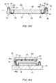
FIG. 14A is a plan view illustrating a plug of FIGS. 10A to 10C, FIG. 14B is an elevation view of the same, and FIG. 14C is a side view of the same.
FIG. 15A is a plan view illustrating a socket of FIGS. 10A to 10C, FIG. 15B is an elevation view of the same, FIG. 15C is a cross-sectional view taken along line F-F of FIG. 15B, and FIG. 15D is a cross-sectional view taken along line E-E of FIG. 15A.
FIGS. 16A, 16B, and 16C are each a partial enlarged cross-sectional view for illustrating the operation of adjusting positional misalignment in the longitudinal direction.
FIGS. 17A, 17B, and 17C are each a partial enlarged cross-sectional view for illustrating the operation of adjusting positional misalignment in the width direction of the same connector.
DETAILED DESCRIPTION
A first embodiment of a substrate connection structure using a substrate connector according to the present invention will now be described based on examples illustrated in FIGS. 1 to 9D. In these figures, reference numerals b1 and b2 denote substrates, respectively. The substrate b1 may be a PCB, and the substrate b2 may be an FPC, for example.
A substrate connector 1 is used for the substrate-to-substrate connection. The substrate b1 and the substrate b2 are connected to each other via the substrate connector 1.
As illustrated in FIGS. 1A to 1C, the substrate connector 1 includes a plug 4 and a socket 7. The plug 4 has plug portions 3 each having an elongated and protruded shape. The plug portion 3 includes a plurality of plug-side signal terminals 2 arranged along a lateral portion thereof. The socket 7 includes a plurality of socket-side signal terminals 6 arranged along inner side surface portions of plug insertion grooves 5 into which the plug portions 3 are to be inserted. Fitting the plug portions 3 into the plug insertion grooves 5 achieves the connection between the plug-side signal terminals 2 and the socket-side signal terminals 6. As a result, the substrates b1 and b2 with the plug 4 and the socket 7 mounted thereon, respectively, are electrically connected to each other via these signal terminals 2 and 6.
Note that a description in the present embodiment will be made with a longitudinal direction of the plug portion 3 being referred to as a longitudinal direction, a horizontal direction perpendicular to the longitudinal direction as a width direction, and a direction in which the plug 4 and the socket 7 face each other as a connection direction.
According to the substrate connector 1, the socket 7 is provided with guiding portions 9, each having a guide groove 8 directed in the connection direction, and the plug 4 is provided with guided portions 10 to be fitted into the guide grooves 8. When connecting the plug 4 and the socket 7 together, the guided portion 10 is guided by an inner side surface of the guide groove 8, thereby enabling the plug portions 3 to be fitted into the respective plug insertion grooves 5 at predetermined positions.
As illustrated in FIGS. 5A to 5C, the plug 4 includes a plug main body 11 made of an insulating resin and having the plug portions 3 of an elongated and protruded shape. The plurality of plug-side signal terminals 2 are integrated with the plug main body 11 by means of insert molding.
The plug main body 11 is integrally formed with an insulating synthetic resin. The plug main body 11 includes: a main body base 12 of a flat-plate shape; the plug portions 3 each having an elongated and protruded shape, protruded from a surface of the main body base 12 and extending in the longitudinal direction; and the guided portions 10 disposed at opposite ends thereof in the longitudinal direction. The main body base 12 and the plug portions 3 together form a shape such that U-shaped cross sections continuously appear in the longitudinal direction. Also, the plug portions 3 and the guided portions 10 disposed at the opposite ends thereof together form a rectangular frame shape as viewed from above.
The guided portion 10 is formed in a cuboid shape. The guided portion 10 integrally has a guide slant portion 13, having a shape bulging toward the socket 7 (the mate side thereof), on a socket-side end face thereof.
The guide slant portion 13 is formed in such a manner that a height of the socket-side end face thereof is greater than that of the plug portions 3. The guide slant portion 13 also has a shape of a truncated square pyramid with guide slant faces 13 a formed along a peripheral portion thereof.
A guide protrusion 14 is provided on the mate-side end face of the guided portion 10 so as to protrude toward the socket 7 side in the connection direction.
The guide protrusion 14 is formed by integrating, by means of insert molding, a plug hold-down member 16 made of a metal plate material with a surface portion of a protrusion base 15 made of an insulating synthetic resin and integrally formed with the guided portion 10. The guide protrusion 14 and the guided portion 10 together form a protruding shape as viewed from the end face thereof in the longitudinal direction.
The plug hold-down member 16 is obtained by bending a conductive metal plate material having a strip shape to be formed in an inverted U-shape with an arc-like top thereof facing upward. The plug hold-down member 16 is integrated with the surface portion of the protrusion base 15 with the outer surface thereof being exposed.
A second-side (the guided portion side) longitudinal-direction guide face 17 is formed at an upper end of the guide protrusion 14 so as to be slidable with a first-side (the guiding portion side) longitudinal-direction guide face, which will be described later and is formed at an edge portion of an opening in the guide groove 8.
The longitudinal-direction guide face 17 is formed by a surface portion of the plug hold-down member 16 so as to have an arc-like cross section bulging upwardly.
The upper end of the protrusion base 15 has slant faces 18 formed along opposite edges thereof in the width direction. The slant faces 18 are slanted toward an inner side in the connection direction. The slant faces 18 form second-side (the guided portion side) width-direction guide faces slidable with first-side (the guiding portion side) width-direction guide faces to be described later.
Furthermore, a top position of the guide protrusion 14, i.e., a length in the connection direction extending from a substrate mounting surface 4 a of the plug 4 to the apex of the guide protrusion 14, is set to be greater than the overall height of the socket 7. The guide protrusion 14 is configured such that it protrudes toward the substrate b2 beyond a mate-side substrate mounting surface 7 a, i.e., the lower surface 7 a of the socket 7 when the plug 4 is fitted into the socket 7.
The socket 7, on the other hand, includes: a socket main body 20 made of an insulating resin material; the plurality of socket-side signal terminals 6; and socket hold-down members 21 made of a conductive metal material as illustrated in FIGS. 6A to 6D. The socket 7 is formed by integrating the socket-side signal terminals 6 and the socket hold-down members 21 with the socket main body 20. The guiding portions 9, each having the guide groove 8, are disposed at opposite ends of a fitting portion 22 of a flat-plate shape.
The fitting portion 22 includes: side walls 24 formed so as to rise from opposite side edges of a flat plate-shaped bottom plate 23 in the width direction; and a central protruding portion 25 disposed at a center portion of the bottom plate 23. The plug insertion grooves 5 each having a recessed groove shape, into which the plug portions 3 are to be inserted, are formed between the side walls 24 and the central protruding portion 25 with a parallel configuration spaced apart from each other in the width direction.
The guiding portions 9 are formed by integrating the socket hold-down members 21 made of a conductive metal plate material with the opposite ends of the socket main body 20. The guiding portions 9 are provided so as to be continuous with the side walls 24 of the fitting portion 22. The guiding portion 9 includes: peripheral walls 26 faced each other in the width direction; and an end wall 27 disposed at an end portion in the longitudinal direction. The guide groove 8 directed in the connection direction is formed by being surrounded by the peripheral walls 26, the end wall 27, and an end face of the fitting portion 22.
The end wall 27 has a first-side (the guiding portion side) longitudinal-direction guide face 28 slanted downwardly toward an inner side in the longitudinal direction at an inner portion of an upper end thereof. The longitudinal-direction guide face 28 slides with the second-side (the guided portion side) longitudinal-direction guide face 17, thereby leading the guide protrusion 14 of the plug 4 to the inner side of the guide groove 8 in the longitudinal direction.
The longitudinal-direction guide face 28 is formed in such a manner that a lower edge thereof is positioned lower than an end face of the fitting portion. Therefore, while keeping the overall height of the socket 7 small, a long distance capable of adjusting positional misalignment is ensured in the longitudinal direction.
An engagement recess 29, having a rectangular cutout shape, is formed at a lower end of the end wall 27 along an inner side surface thereof. An engagement protrusion 30, protruding from the surface of the plug hold-down member 16, is engaged with the engagement recess 29 when the plug 4 is fitted into the socket 7, thereby fixing the plug 4 to the socket 7.
The peripheral wall 26 includes a first-side (the guiding portion side) width-direction guide face 31 slanted downwardly toward an inner side in the width direction. The width-direction guide face 31 slides with the second-side (the guided portion side) width-direction guide face 18, thereby leading the guide protrusion 14 of the plug 4 to the inner side of the guide groove 8 in the width direction.
The width-direction guide faces 31 are disposed at opposite ends of the longitudinal-direction guide face 28 in the width direction, respectively. The longitudinal-direction guide face 28 and the width-direction guide faces 31 together form a U-shape as viewed from above.
An escape hole 32, in communication with the guide groove 8 in the connection direction and passing completely through the substrate mounting surface 7 a, is provided at the bottom of the guiding portion 9. When the plug 4 is fitted into the socket 7, the guide protrusion 14 provided in the guided portion 10 protrudes farther beyond the socket-side substrate mounting surface 7 a through the escape hole 32.
On the other hand, as illustrated in FIG. 7, the substrate b2, onto which the socket 7 is mounted, is provided with escape cutout portions 33 at positions corresponding to the mounting position of the socket 7. The escape cutout portion 33 has a hole shape or a cutout shape, and the guide protrusion 14 is inserted therein.
Note that reference numerals 34 represent signal flow patterns formed on the surface of the substrate b2 and reference numerals 35 represent fixation patterns. Connection terminals 6 a in the socket-side signal terminals 6 are soldered to the signal flow patterns 34, respectively, and peripheral wall portions of the socket hold-down members 21 are soldered to the fixation patterns 35. As a result, the socket 7 can be mounted on the substrate b2 at a predetermined position.
The escape cutout portions 33 are formed by cutting out opposite side edge portions of the substrate b2 in a recessed shape. The escape cutout portion 33 is formed so as to be continuous with the guide groove 8 and the escape hole 32 of the socket 7 in the connection direction of the connector. The escape cutout portion 33 is provided in order to prevent the guide protrusion 14, protruded farther beyond the mounting surface 7 a through the escape hole 32 when the plug 4 is fitted into the socket 7, from interfering with the substrate b2.
According to the thus configured substrate connector 1, if a relative position between the plug 4 and the socket 7 is misaligned in the horizontal direction, the guide protrusion 14 is guided by the inner side surface of the guide groove 8, thereby leading the guided portion 10 to the inner side surface portion of the guide groove 8. Then, the outer side surface of the guided portion 10 is guided by the inner side surface of the guide groove 8, thereby enabling the plug 4 to be fitted into the socket 7 at the predetermined position.
In other words, in a case where a relative position between the plug 4 and the socket 7 is misaligned in the longitudinal direction as illustrated in FIG. 8A, the longitudinal-direction guide face 17 of the guide protrusion 14 first comes in contact with the longitudinal-direction guide face 28. As illustrated in FIGS. 8A and 8B, the longitudinal-direction guide faces 17 and 28 then slide with each other, thereby leading the guide protrusion 14 to the inner side of the guide groove 8 in the longitudinal direction.
An outer side surface of the guide protrusion 14 in the longitudinal direction is guided by an inner side surface 8 a of the guide groove 8, thereby leading the outer side surface of the guided portion 10 to the inner side of the guide groove 8 in the longitudinal direction. The outer side surface of the guided portion 10 is further guided by the inner side surface 8 a of the guide groove 8 in the longitudinal direction. Consequently, the plug 4 is fitted into the socket 7 at the predetermined position, and the guide protrusion 14, provided in the guided portion 10, protrudes farther beyond the substrate mounting surface 7 a of the socket 7 through the escape hole 32 and is inserted into the escape cutout portion 33 of the substrate b2.
As described above, even if the first-side (the guiding portion side) longitudinal-direction guide face 28 is formed in such a manner that the lower edge thereof is positioned lower than the end face of the fitting portion 22 so as to ensure a wide range of distance capable of adjusting positional misalignment in the longitudinal direction while keeping the overall height of the socket 7 small, the substrate connection structure using the substrate connector 1 enables the plug 4 to be reliably fitted into the socket 7 at the predetermined position, thereby preventing unintended contact. This is achieved by the provision of the guide protrusion 14 at the mate-side end face of the guided portion 10. This is because the guide protrusion 14 is always led to the inner side surface 8 a of the guide groove 8 in the longitudinal direction before being touched by any other portion and the guided portion 10 is led to the inner side surface of the guide groove 8 by the guide protrusion 14 being guided by the guide groove 8.
On the other hand, if a relative position between the plug 4 and the socket 7 is misaligned in the width direction as illustrated in FIG. 9A, the second-side (the guided portion side) width-direction guide face 18 in the guide protrusion 14 first comes into contact with the first-side (the guiding portion side) width-direction guide face 31 in the socket 7. As illustrated in FIGS. 9A and 9B, the width-direction guide faces 18 and 31 then slide with each other, thereby leading the guide protrusion 14 to the inner side of the guide groove 8 in the width direction.
An outer side surface of the guide protrusion 14 is guided by an inner side surface 8 b of the guide groove 8, thereby allowing the guide slant portion 13 of the guided portion 10 to be in contact with the width-direction guide face 31 as illustrated in FIGS. 9B and 9C. The width-direction guide face 31 and the width-direction slant face 13 a of the guide slant portion 13 then slide with each other, thereby leading the outer side surface of the guided portion 10 to the inner side of the guide groove 8 in the width direction.
The outer side surface of the guided portion 10 is further guided by the inner side surface 8 b of the guide groove 8 in the width direction as illustrated in FIGS. 9C and 9D. Consequently, the plug 4 is fitted into the socket 7 at the predetermined position, and the guide protrusion 14 provided in the guided portion 10 protrudes farther beyond the substrate mounting surface 7 a of the socket 7 through the escape hole 32 and is inserted into the escape cutout portion 33 of the substrate b2.
Thus, according to the substrate connection structure using the substrate connector 1, the guide protrusion 14 is provided in the guided portion 10 so as to allow the second-side (the guided portion side) width-direction guide face 18 in the guide protrusion 14 to slide with the first-side (the guiding portion side) width-direction guide face 31 in the guide groove for guiding. It is therefore possible to ensure a correspondingly longer distance capable of adjusting positional misalignment.
If a relative position between the plug 4 and the socket 7 is misaligned in both of the longitudinal direction and the width direction, the above-described operations illustrated in FIGS. 8A to 9D are performed in a combined manner so as to lead the guided portion 10 to the inner side of the guide groove 8.
Since the guide protrusions 14 are configured to protrude farther beyond the mate-side substrate mounting surface 7 a and, at the same time, interference between the guide protrusions 14 and the mate-side substrate b2 is prevented from occurring, a distance between the substrates b1 and b2 when connected can be kept small even when the guide protrusion 14 is provided.
Furthermore, the positions of the guide protrusion 14 and the guided portion 10 can be visually checked through the guide groove 8, the escape hole 32, and the escape cutout portion 33. It is therefore possible to efficiently perform a connecting operation between the substrate b1 and the substrate b2.
A second embodiment of the substrate connection structure using the substrate connector according to the present invention will now be described below based on examples shown in FIGS. 10A to 17C. Note that reference numerals b3 and b4 denote substrates, respectively. The substrate b3 may be an FPC, and the substrate b4 may be a PCB, for example.
This substrate connection structure employs a substrate connector 42 formed by a plug 40 and a socket 41 mounted on the substrates b3 and b4 respectively. The substrate b3 and the substrate b4 are connected to each other via the substrate connector 42.
As illustrated in FIGS. 14A to 14C, the plug 40 includes a plug main body 44 made of an insulating resin and having plug portions 43 of an elongated and protruded shape. A plurality of plug-side signal terminals 45 are integrated with the plug main body 44 by means of insert molding.
The plug main body 44 is integrally formed with an insulating synthetic resin. The plug main body 44 includes: a main body base 46 of a flat-plate shape; the plug portions 43 each having an elongated and protruded shape, protruded from a surface of the main body base 46 and extending in the longitudinal direction; and guided portions 47 disposed at opposite ends thereof in the longitudinal direction. The main body base 46 and the plug portions 43 together form a shape such that U-shaped cross sections continuously appear in the longitudinal direction. Also, the plug portions 43 and the guided portions 47 disposed at the opposite ends thereof together form a rectangular frame shape as viewed from above.
The guided portion 47 is formed in a cuboid shape. The guided portion 47 integrally has a guide portion 48, having a shape bulging toward the socket 41 (the mate side), at a socket-side end face thereof.
The guide portion 48 is formed in such a manner that a height of the socket-side end face thereof is greater than that of the plug portions 43. Also, the guide portion 48 has a truncated square pyramid shape including: a first-side (the guided portion side) longitudinal-direction guide face 48 a formed by a slant surface and provided at a peripheral portion thereof in the longitudinal direction; and first-side (the guided portion side) width-direction guide faces 48 b formed by slant surfaces and provided at opposite side edges thereof in the width direction.
As illustrated in FIG. 14B, the lower edges of the guide faces 48 a and 48 b are positioned so as to be lower than the top of the plug portion 43. Therefore, large distances of the guide faces 48 a and 48 b in the horizontal direction, i.e., distances capable of adjusting positional misalignment, are ensured while keeping the overall height of the plug 40 small correspondingly.
Note that reference numeral 49 denotes a plug hold-down member being integrated with the plug main body 44 by means of insert molding.
The substrate b3, onto which the plug 40 is mounted, is provided with escape cutout portions 50 at opposite side edge portions thereof corresponding to the mounting position of the plug 40. The escape cutout portion 50 has a hole shape or a cutout shape, and a guide protrusion to be described later is inserted therein. When the plug 40 is mounted on the substrate b3, the opposite ends of the plug 40 are exposed through the respective escape cutout portions 50, thereby allowing for the visual check of the positions thereof.
The socket 41, on the other hand, includes: a socket main body 60 made of an insulating resin material; a plurality of socket-side signal terminals 61; and socket hold-down members 62 made of a conductive metal material as illustrated in FIGS. 15A to 15D. The socket 41 is formed by integrating the socket-side signal terminals 61 and the socket hold-down members 62 with the socket main body 60. Guiding portions 65, each having a guide groove 64, are disposed at opposite ends of a fitting portion 63 of a flat-plate shape.
The fitting portion 63 includes: side walls 67 formed so as to rise from opposite side edges of a flat plate-shaped bottom plate 66 in the width direction; and a central protruding portion 68 disposed at a center portion of the bottom plate 66. Plug insertion grooves 69 each having a recessed groove shape, into which the plug portions 43 are to be inserted, are formed between the side walls 67 and the central protruding portion 68 with a parallel configuration spaced apart from each other in the width direction.
The guiding portions 65 are formed by integrating the socket hold-down members 62, made of a conductive metal plate material, with the opposite ends of the socket main body 60. The guiding portions 65 are provided so as to be continuous with the side walls 67 of the fitting portion 63. The guiding portions 65 include: peripheral walls 70 faced each other in the width direction; and end walls 71 disposed at opposite ends in the longitudinal direction. The guide groove 64 directed in the connection direction is formed by being surrounded by the peripheral walls 70, the end wall 71, and an end face of the fitting portion 63.
A guide protrusion 80 is provided on the mate-side (i.e., the plug 40 side) end face of the guiding portion 65 so as to protrude toward the plug side in the connection direction.
The guide protrusion 80 is provided over an area extending from the end wall 71 to the peripheral walls 70. The top position of the guide protrusion 80, i.e., a distance in the vertical direction from a substrate mounting surface 41 a of the socket 41 to the apex of the guide protrusion 80, is set to be greater than the overall height of the plug 40. When the plug 40 is fitted into the socket 41, the guide protrusions 80 pass laterally to the opposite ends of the plug 40 in the longitudinal direction and protrude farther toward the substrate b3 beyond a mate-side substrate mounting surface 40 a, i.e., the lower surface 40 a of the plug 40.
The guide protrusion 80 includes, at inner side surface portions thereof, a second-side (the guiding portion side) longitudinal-direction guide face 81 and second-side (the guiding portion side) width-direction guide faces 82 so as to be continuous with the guide groove 64. The second-side (the guiding portion side) longitudinal-direction guide face 81 and the first-side (the guided portion side) longitudinal-direction guide face 48 a slide with each other, and the second-side (the guiding portion side) width-direction guide faces 82 and the first-side (the guided portion side) width-direction guide faces 48 b slide with each other. As a result, the guided portion 47 is led into the guide groove 64.
The longitudinal-direction guide face 81 is formed in a shape slanted downwardly toward the inner side in the longitudinal direction. A longitudinal-direction inner side surface 64 a of the guide groove 64 is formed downwardly in the vertical direction continuously from the lower edge of the longitudinal-direction guide face 81.
The width-direction guide faces 82 each are formed in a shape slanted downwardly toward the inner side in the width direction. The width-direction guide faces 82 are disposed at the opposite ends of the longitudinal-direction guide face 81. The longitudinal-direction guide face 81 and the width-direction guide faces 82 together form a U-shape as viewed from above.
An engagement recess 83, having a rectangular cutout shape, is formed at a lower end of the end wall 71 along an inner side surface portion thereof. An engagement protrusion 84, protruding from the surface of the plug hold-down member 49, is engaged with the engagement recess 83 when the plug 40 is fitted into the socket 41, thereby fixing the plug 40 to the socket 41.
According to the thus configured substrate connector 42, if a relative position between the plug 40 and the socket 41 is misaligned in the horizontal direction, the guided portion 47 is guided by the guide protrusion 80, thereby being led to the inner side of the guide groove 64. Then, the outer side surface of the guided portion 47 is guided by the inner side surface of the guide groove 64, thereby enabling the plug 40 to be fitted into the socket 41 at the predetermined position.
In other words, in a case where a relative position between the plug 40 and the socket 41 is misaligned in the longitudinal direction as illustrated in FIG. 16A, the first-side longitudinal-direction guide face 48 a in the guided portion 47 first comes into contact with the second-side longitudinal-direction guide face 81 in the guide protrusion 80. As illustrated in FIGS. 16A and 16B, the longitudinal-direction guide faces 48 a and 81 then slide with each other, thereby leading the guided portion 47 to the inner side of the guide groove 64 in the longitudinal direction.
Then, an outer side surface of the guided portion 47 is guided by the inner side surface 64 a of the guide groove 64 in the longitudinal direction, thereby enabling the plug 40 to be fitted into the socket 41 at the predetermined position. The guide protrusions 80 pass laterally to the opposite ends of the plug 40 in the longitudinal direction and protrude farther toward the substrate b3 beyond the substrate mounting surface 40 a of the plug 40.
Providing the escape cutout portions 50 in the substrate b3 prevents interference between the guide protrusions 80 and the substrate b3 from occurring on such an occasion.
On the other hand, if a relative position between the plug 40 and the socket 41 is misaligned in the width direction as illustrated in FIG. 17A, the width-direction guide face 48 b of the guided portion 47 first comes into contact with one of the width-direction guide faces 82 in the guide protrusion 80. As illustrated in FIGS. 17A and 17B, the width-direction guide faces 48 b and 82 then slide with each other, thereby leading the guided portion 47 to the inner side of the guide groove 64 in the width direction.
Then, as illustrated in FIGS. 17B and 17C, the outer side surface of the guided portion 47 is guided by the inner side surface 64 b of the guide groove 64 in the width direction, thereby enabling the plug 40 to be fitted into the socket 41 at the predetermined position. The guide protrusions 80 pass laterally to the opposite ends of the plug 40 in the longitudinal direction and protrude farther beyond the substrate mounting surface 40 a.
Providing the escape cutout portions 50 in the substrate b3 prevents interference between the guide protrusions 80 and the substrate b3 from occurring on such an occasion.
If a relative position between the plug 40 and the socket 41 is misaligned in both of the longitudinal direction and the width direction, the above-described operations illustrated in FIGS. 16A to 17C are performed in a combined manner so as to lead the guided portion 47 to the inner side of the guide groove 64.
Even if the first-side guide faces 48 a and 48 b are formed in such a manner that the lower edges thereof are positioned lower than the end face of the plug portion 43 so as to ensure a wide range of distance capable of adjusting positional misalignment while keeping the overall height of the plug 40 small, the substrate connection structure using the thus configured substrate connector 42 can prevent unintended contact between the plug 40 and the socket 41 by the provision of the guide protrusion 80 at the mate-side end face of the guiding portion 65. This is because the guided portion 47 is always led to the inner side of the guide groove 64 by the guide protrusion 80 before being touched by any other portion.
Since the guide protrusions 80 are configured to protrude farther beyond the mate-side substrate mounting surface 40 a and, at the same time, interference between the guide protrusions 80 and the mate-side substrate b3 is prevented from occurring, a distance between the substrates when connected can be kept small.
Furthermore, the positions of the guide protrusions 80 and the plug 40 can be visually checked through the opposite end portions of the substrate b3. It is therefore possible to efficiently perform connection between the substrates b3 and b4.
The above-described embodiments describe a case where the recessed escape cutout portions are provided in the substrate b2 or b3 in order to avoid interference between the guide protrusions and the mate-side substrate. However, a mode for avoiding interference between the guide protrusions and the mate-side substrate is not limited to the above-described embodiments. For example, hole-shaped escape cutout portions may be provided. Also, a width of the substrates b2 and b3 may be formed smaller than a distance between the opposite guide protrusions so that the guide protrusions protrude laterally to the side edge portions of the substrates b2 and b3.
The configurations of the plugs 4 and 40 and the sockets 7 and 41 are not limited to those described in the embodiments above. For example, a configuration including a single plug portion 3 or 43 may be employed. Alternatively, three or more plug portions may be provided.
The case where the guided portions are provided in the plug and the guiding portions are provided in the socket has been described in the above-described embodiments. Depending on the structure, however, the guiding portions may be provided in the plug and the guided portions may be provided in the socket.
LIST OF REFERENCE SIGNS
    • b1 Substrate (PCB)
    • b2 Substrate (FCP)
    • 1 Substrate connector (42)
    • 2 Plug-side signal terminal
    • 3 Plug portion
    • 4 Plug
    • 5 Plug insertion groove
    • 6 Socket-side signal terminal
    • 7 Socket (41)
    • 8 Guide groove
    • 9 Guiding portion
    • 10 Guided portion
    • 11 Plug main body
    • 12 Main body base
    • 13 Guide slant portion
    • 14 Guide protrusion
    • 15 Protrusion base
    • 16 Plug hold-down member (49)
    • 17 Longitudinal-direction guide face
    • 18 Width-direction guide face (slant face)
    • 20 Socket main body
    • 21 Socket (41) hold-down member
    • 22 Fitting portion
    • 23 Bottom plate
    • 24 Side wall
    • 25 Central protruding portion
    • 26 Peripheral wall
    • 27 End wall
    • 28 Socket (41) side guide face
    • 29 Engagement recess
    • 30 Engagement protrusion
    • 31 Socket (41) side guide face
    • 32 Escape hole
    • 33 Escape cutout portion
    • 34 Signal flow pattern
    • 35 Fixation pattern
    • b3 Substrate (FPC)
    • b4 Substrate (PCB)
    • 40 Plug
    • 41 Socket
    • 42 Substrate connector
    • 43 Plug portion
    • 44 Plug main body
    • 45 Plug-side signal terminal
    • 46 Main body base
    • 47 Guided portion
    • 48 Guide portion
    • 49 Plug hold-down member
    • 50 Escape cutout portion
    • 60 Socket main body
    • 61 Socket-side signal terminal
    • 62 Socket hold-down member
    • 63 Fitting portion
    • 64 Guide groove
    • 65 Guiding portion
    • 66 Bottom plate
    • 67 Side wall
    • 68 Central protruding portion
    • 69 Plug insertion groove
    • 70 Peripheral wall
    • 71 End wall
    • 80 Guide protrusion
    • 81 Longitudinal-direction guide face
    • 82 Width-direction guide face
    • 83 Engagement recess
    • 84 Engagement protrusion

Claims (3)

The invention claimed is:
1. A substrate connection structure using a substrate connector, the substrate connector including a plug and a socket to be mounted on substrates, respectively, and fitted together, one of the plug and the socket including a guiding portion having a guide groove directed in a connection direction, the other of the plug and the socket including a guided portion to be fitted into the guide groove, the guided portion being guided by an inner side surface of the guide groove, thereby enabling the plug to be fitted into the socket at a predetermined position, wherein
a guide protrusion is provided at a mate-side end face of the guided portion and/or the guiding portion so as to protrude farther beyond a mate-side substrate mounting surface when the plug is fitted into the socket,
a first-side guide face is formed in the guided portion or an edge portion of an opening in the guide groove and the guide protrusion is provided with a second-side guide face slidable with the first-side guide face so as to lead the guided portion into the guide groove, and interference between the guide protrusion and the mate-side substrate is prevented from occurring.
2. The substrate connection structure according to claim 1, wherein an escape hole, in communication with the guide groove and passing completely through the mate-side substrate mounting surface, is provided in the guiding portion and the guide protrusion provided in the guided portion protrudes farther beyond the mate-side substrate mounting surface through the escape hole.
3. The substrate connection structure according to claim 1, wherein an escape cutout portion having any of a hole shape and a cutout shape for the guide protrusion to be inserted therein is provided in the substrate.
US14/159,385 2013-04-19 2014-01-20 Substrate connection structure using substrate connector Expired - Fee Related US9196984B2 (en)

Applications Claiming Priority (2)

Application Number Priority Date Filing Date Title
JP2013-088043 2013-04-19
JP2013088043A JP5751434B2 (en) 2013-04-19 2013-04-19 Board connection structure using board connector

Publications (2)

Publication Number Publication Date
US20140315419A1 US20140315419A1 (en) 2014-10-23
US9196984B2 true US9196984B2 (en) 2015-11-24

Family

ID=51709642

Family Applications (1)

Application Number Title Priority Date Filing Date
US14/159,385 Expired - Fee Related US9196984B2 (en) 2013-04-19 2014-01-20 Substrate connection structure using substrate connector

Country Status (4)

Country Link
US (1) US9196984B2 (en)
JP (1) JP5751434B2 (en)
KR (1) KR101629640B1 (en)
CN (1) CN104112946B (en)

Cited By (5)

* Cited by examiner, † Cited by third party
Publication number Priority date Publication date Assignee Title
US20160268715A1 (en) * 2015-02-16 2016-09-15 Tyco Electronics Japan G.K. Connector
US20190288420A1 (en) * 2018-03-13 2019-09-19 Japan Aviation Electronics Industry, Limited Plug, receptacle, and connector
KR20200004891A (en) * 2017-07-24 2020-01-14 가부시키가이샤 무라타 세이사쿠쇼 Connector set
US11005200B2 (en) 2018-08-24 2021-05-11 Japan Aviation Electronics Industry, Limited Connector assembly and connector
US11355882B2 (en) * 2016-11-18 2022-06-07 Molex, Llc Board-to-board connector

Families Citing this family (8)

* Cited by examiner, † Cited by third party
Publication number Priority date Publication date Assignee Title
JP6056835B2 (en) 2014-11-14 2017-01-11 第一精工株式会社 Electric connector for board connection and electric connector device for board connection
JP6136078B2 (en) * 2015-02-09 2017-05-31 Smk株式会社 Board connector device
JP6378642B2 (en) 2015-04-23 2018-08-22 モレックス エルエルシー connector
CN105428912A (en) * 2015-12-28 2016-03-23 苏州卓德电子有限公司 Wiring harness connector
JP2018120654A (en) * 2017-01-23 2018-08-02 ヒロセ電機株式会社 Connector assembly and connector device using the same
JP2018129150A (en) * 2017-02-07 2018-08-16 第一精工株式会社 Electric connector
JP7038172B2 (en) * 2020-10-12 2022-03-17 モレックス エルエルシー connector
CN113099627A (en) * 2021-03-19 2021-07-09 杭州电子科技大学 Auxiliary positioning device for electronic device production

Citations (2)

* Cited by examiner, † Cited by third party
Publication number Priority date Publication date Assignee Title
US7195494B2 (en) * 2004-03-31 2007-03-27 Matsushita Electric Works, Ltd., Connector for electrically connecting electronic components
JP2010097724A (en) 2008-10-14 2010-04-30 Molex Inc Board-to-board connector

Family Cites Families (9)

* Cited by examiner, † Cited by third party
Publication number Priority date Publication date Assignee Title
JPH10214659A (en) * 1997-01-29 1998-08-11 Sumitomo Wiring Syst Ltd Sheetlike conductive path connector
JPH1174024A (en) * 1997-08-29 1999-03-16 Omron Corp Electric connector
JP3732709B2 (en) * 2000-03-28 2006-01-11 ヒロセ電機株式会社 Electrical connector
JP3949064B2 (en) * 2003-02-06 2007-07-25 ヒロセ電機株式会社 Electrical connector
JP3875211B2 (en) * 2003-04-25 2007-01-31 ヒロセ電機株式会社 Electrical connector connection structure
JP2006210206A (en) * 2005-01-31 2006-08-10 Kyocera Elco Corp Connector and portable terminal
JP2006244902A (en) * 2005-03-04 2006-09-14 Tyco Electronics Amp Kk Electric connector and electric connector assembly
JP2007018993A (en) * 2005-06-07 2007-01-25 Kyocera Elco Corp Connector and portable terminal
WO2012033913A2 (en) * 2010-09-08 2012-03-15 Molex Incorporated Circuit board-circuit board connector

Patent Citations (2)

* Cited by examiner, † Cited by third party
Publication number Priority date Publication date Assignee Title
US7195494B2 (en) * 2004-03-31 2007-03-27 Matsushita Electric Works, Ltd., Connector for electrically connecting electronic components
JP2010097724A (en) 2008-10-14 2010-04-30 Molex Inc Board-to-board connector

Cited By (8)

* Cited by examiner, † Cited by third party
Publication number Priority date Publication date Assignee Title
US20160268715A1 (en) * 2015-02-16 2016-09-15 Tyco Electronics Japan G.K. Connector
US11355882B2 (en) * 2016-11-18 2022-06-07 Molex, Llc Board-to-board connector
KR20200004891A (en) * 2017-07-24 2020-01-14 가부시키가이샤 무라타 세이사쿠쇼 Connector set
US20200161816A1 (en) * 2017-07-24 2020-05-21 Murata Manufacturing Co., Ltd. Connector set
US10910779B2 (en) * 2017-07-24 2021-02-02 Murata Manufacturing Co., Ltd. Board-to-board electrical connector set having projecting portions and guiding portions
US20190288420A1 (en) * 2018-03-13 2019-09-19 Japan Aviation Electronics Industry, Limited Plug, receptacle, and connector
US10763604B2 (en) * 2018-03-13 2020-09-01 Japan Aviation Electronics Industry, Limited Plug, receptacle, and connector
US11005200B2 (en) 2018-08-24 2021-05-11 Japan Aviation Electronics Industry, Limited Connector assembly and connector

Also Published As

Publication number Publication date
KR20140125708A (en) 2014-10-29
US20140315419A1 (en) 2014-10-23
CN104112946B (en) 2016-06-01
KR101629640B1 (en) 2016-06-13
CN104112946A (en) 2014-10-22
JP2014212049A (en) 2014-11-13
JP5751434B2 (en) 2015-07-22

Similar Documents

Publication Publication Date Title
US9196984B2 (en) Substrate connection structure using substrate connector
JP7103454B2 (en) Electrical connector device for board connection
US10879635B2 (en) Electrical connector
CN106410457B (en) Electrical connector for substrate connection
US8105112B2 (en) Electrical connector
US7207842B1 (en) Electrical connector
EP3696921A1 (en) Connector
US7744377B2 (en) Electrical connector with low profile contacts
KR101383455B1 (en) Electric connector
EP3660985A1 (en) Connector
US11605911B2 (en) Electrical connector including plug connector and receptacle connector detachably fitting to each other
US10381776B2 (en) Connector assembly with an improved latch member having a shorter length
US8986020B2 (en) Inter-terminal connection structure
US20130137307A1 (en) Plug connector, receptacle connector and electrical connector assembly
US7607943B2 (en) Electric connector for circuit board
JP5530278B2 (en) Connector assembly
KR101652383B1 (en) Connector
KR20150001574A (en) Connector
TWI628881B (en) Connector device for substrate connection
US20070254507A1 (en) Electrical connector with improved contacts
US8500459B2 (en) Receptacle with a cavity for receiving a plug with a recess for receiving a component
JP5790950B2 (en) Board connector
KR20140147646A (en) Connector

Legal Events

Date Code Title Description
AS Assignment

Owner name: SMK CORPORATION, JAPAN

Free format text: ASSIGNMENT OF ASSIGNORS INTEREST;ASSIGNORS:ISHIDA, YOSHIYASU;OHSAWA, FUMIO;ASAI, KIYOSHI;REEL/FRAME:032013/0633

Effective date: 20131212

STCF Information on status: patent grant

Free format text: PATENTED CASE

FEPP Fee payment procedure

Free format text: MAINTENANCE FEE REMINDER MAILED (ORIGINAL EVENT CODE: REM.); ENTITY STATUS OF PATENT OWNER: LARGE ENTITY

LAPS Lapse for failure to pay maintenance fees

Free format text: PATENT EXPIRED FOR FAILURE TO PAY MAINTENANCE FEES (ORIGINAL EVENT CODE: EXP.); ENTITY STATUS OF PATENT OWNER: LARGE ENTITY

STCH Information on status: patent discontinuation

Free format text: PATENT EXPIRED DUE TO NONPAYMENT OF MAINTENANCE FEES UNDER 37 CFR 1.362

FP Expired due to failure to pay maintenance fee

Effective date: 20191124