EP1947633B1 - Organic light emitting display - Google Patents
Organic light emitting display Download PDFInfo
- Publication number
- EP1947633B1 EP1947633B1 EP08250060.4A EP08250060A EP1947633B1 EP 1947633 B1 EP1947633 B1 EP 1947633B1 EP 08250060 A EP08250060 A EP 08250060A EP 1947633 B1 EP1947633 B1 EP 1947633B1
- Authority
- EP
- European Patent Office
- Prior art keywords
- electrode
- organic light
- light emitting
- power supply
- switching transistor
- Prior art date
- Legal status (The legal status is an assumption and is not a legal conclusion. Google has not performed a legal analysis and makes no representation as to the accuracy of the status listed.)
- Active
Links
- 239000003990 capacitor Substances 0.000 claims description 89
- 238000010586 diagram Methods 0.000 description 22
- 238000000034 method Methods 0.000 description 14
- 238000002425 crystallisation Methods 0.000 description 10
- 239000000463 material Substances 0.000 description 9
- 239000010409 thin film Substances 0.000 description 9
- 108010075750 P-Type Calcium Channels Proteins 0.000 description 8
- 230000008025 crystallization Effects 0.000 description 7
- 238000005499 laser crystallization Methods 0.000 description 5
- 230000008569 process Effects 0.000 description 5
- 229910021417 amorphous silicon Inorganic materials 0.000 description 4
- 230000010354 integration Effects 0.000 description 4
- 239000002184 metal Substances 0.000 description 4
- 229910052751 metal Inorganic materials 0.000 description 4
- 229910021420 polycrystalline silicon Inorganic materials 0.000 description 4
- 229920005591 polysilicon Polymers 0.000 description 4
- 230000004044 response Effects 0.000 description 4
- 239000000758 substrate Substances 0.000 description 4
- 230000032683 aging Effects 0.000 description 3
- 230000015556 catabolic process Effects 0.000 description 3
- 238000006731 degradation reaction Methods 0.000 description 3
- 230000003071 parasitic effect Effects 0.000 description 3
- 108090000699 N-Type Calcium Channels Proteins 0.000 description 2
- 102000004129 N-Type Calcium Channels Human genes 0.000 description 2
- 238000000137 annealing Methods 0.000 description 2
- 230000003197 catalytic effect Effects 0.000 description 2
- 239000003086 colorant Substances 0.000 description 2
- 239000000203 mixture Substances 0.000 description 2
- 239000007790 solid phase Substances 0.000 description 2
- 238000007711 solidification Methods 0.000 description 2
- 230000008023 solidification Effects 0.000 description 2
- 230000009286 beneficial effect Effects 0.000 description 1
- 230000008859 change Effects 0.000 description 1
- 230000003247 decreasing effect Effects 0.000 description 1
- 238000005401 electroluminescence Methods 0.000 description 1
- 239000011521 glass Substances 0.000 description 1
- 238000005224 laser annealing Methods 0.000 description 1
- 239000004973 liquid crystal related substance Substances 0.000 description 1
- 239000011159 matrix material Substances 0.000 description 1
- 150000002739 metals Chemical class 0.000 description 1
- 230000007704 transition Effects 0.000 description 1
Images

Classifications
-
- G—PHYSICS
- G09—EDUCATION; CRYPTOGRAPHY; DISPLAY; ADVERTISING; SEALS
- G09G—ARRANGEMENTS OR CIRCUITS FOR CONTROL OF INDICATING DEVICES USING STATIC MEANS TO PRESENT VARIABLE INFORMATION
- G09G3/00—Control arrangements or circuits, of interest only in connection with visual indicators other than cathode-ray tubes
- G09G3/20—Control arrangements or circuits, of interest only in connection with visual indicators other than cathode-ray tubes for presentation of an assembly of a number of characters, e.g. a page, by composing the assembly by combination of individual elements arranged in a matrix no fixed position being assigned to or needed to be assigned to the individual characters or partial characters
- G09G3/22—Control arrangements or circuits, of interest only in connection with visual indicators other than cathode-ray tubes for presentation of an assembly of a number of characters, e.g. a page, by composing the assembly by combination of individual elements arranged in a matrix no fixed position being assigned to or needed to be assigned to the individual characters or partial characters using controlled light sources
- G09G3/30—Control arrangements or circuits, of interest only in connection with visual indicators other than cathode-ray tubes for presentation of an assembly of a number of characters, e.g. a page, by composing the assembly by combination of individual elements arranged in a matrix no fixed position being assigned to or needed to be assigned to the individual characters or partial characters using controlled light sources using electroluminescent panels
- G09G3/32—Control arrangements or circuits, of interest only in connection with visual indicators other than cathode-ray tubes for presentation of an assembly of a number of characters, e.g. a page, by composing the assembly by combination of individual elements arranged in a matrix no fixed position being assigned to or needed to be assigned to the individual characters or partial characters using controlled light sources using electroluminescent panels semiconductive, e.g. using light-emitting diodes [LED]
- G09G3/3208—Control arrangements or circuits, of interest only in connection with visual indicators other than cathode-ray tubes for presentation of an assembly of a number of characters, e.g. a page, by composing the assembly by combination of individual elements arranged in a matrix no fixed position being assigned to or needed to be assigned to the individual characters or partial characters using controlled light sources using electroluminescent panels semiconductive, e.g. using light-emitting diodes [LED] organic, e.g. using organic light-emitting diodes [OLED]
- G09G3/3225—Control arrangements or circuits, of interest only in connection with visual indicators other than cathode-ray tubes for presentation of an assembly of a number of characters, e.g. a page, by composing the assembly by combination of individual elements arranged in a matrix no fixed position being assigned to or needed to be assigned to the individual characters or partial characters using controlled light sources using electroluminescent panels semiconductive, e.g. using light-emitting diodes [LED] organic, e.g. using organic light-emitting diodes [OLED] using an active matrix
- G09G3/3233—Control arrangements or circuits, of interest only in connection with visual indicators other than cathode-ray tubes for presentation of an assembly of a number of characters, e.g. a page, by composing the assembly by combination of individual elements arranged in a matrix no fixed position being assigned to or needed to be assigned to the individual characters or partial characters using controlled light sources using electroluminescent panels semiconductive, e.g. using light-emitting diodes [LED] organic, e.g. using organic light-emitting diodes [OLED] using an active matrix with pixel circuitry controlling the current through the light-emitting element
-
- A—HUMAN NECESSITIES
- A45—HAND OR TRAVELLING ARTICLES
- A45D—HAIRDRESSING OR SHAVING EQUIPMENT; EQUIPMENT FOR COSMETICS OR COSMETIC TREATMENTS, e.g. FOR MANICURING OR PEDICURING
- A45D8/00—Hair-holding devices; Accessories therefor
- A45D8/02—Hair pins
-
- A—HUMAN NECESSITIES
- A45—HAND OR TRAVELLING ARTICLES
- A45D—HAIRDRESSING OR SHAVING EQUIPMENT; EQUIPMENT FOR COSMETICS OR COSMETIC TREATMENTS, e.g. FOR MANICURING OR PEDICURING
- A45D8/00—Hair-holding devices; Accessories therefor
- A45D8/20—Hair clamps, i.e. elastic multi-part clamps, the parts of which are pivotally connected between their ends
- A45D8/22—Hair clamps, i.e. elastic multi-part clamps, the parts of which are pivotally connected between their ends with additional fastener
-
- A—HUMAN NECESSITIES
- A45—HAND OR TRAVELLING ARTICLES
- A45D—HAIRDRESSING OR SHAVING EQUIPMENT; EQUIPMENT FOR COSMETICS OR COSMETIC TREATMENTS, e.g. FOR MANICURING OR PEDICURING
- A45D8/00—Hair-holding devices; Accessories therefor
- A45D8/24—Hair clasps, i.e. multi-part clasps with pivotal connection of parts at their ends
-
- G—PHYSICS
- G09—EDUCATION; CRYPTOGRAPHY; DISPLAY; ADVERTISING; SEALS
- G09G—ARRANGEMENTS OR CIRCUITS FOR CONTROL OF INDICATING DEVICES USING STATIC MEANS TO PRESENT VARIABLE INFORMATION
- G09G2300/00—Aspects of the constitution of display devices
- G09G2300/08—Active matrix structure, i.e. with use of active elements, inclusive of non-linear two terminal elements, in the pixels together with light emitting or modulating elements
- G09G2300/0809—Several active elements per pixel in active matrix panels
- G09G2300/0819—Several active elements per pixel in active matrix panels used for counteracting undesired variations, e.g. feedback or autozeroing
-
- G—PHYSICS
- G09—EDUCATION; CRYPTOGRAPHY; DISPLAY; ADVERTISING; SEALS
- G09G—ARRANGEMENTS OR CIRCUITS FOR CONTROL OF INDICATING DEVICES USING STATIC MEANS TO PRESENT VARIABLE INFORMATION
- G09G2300/00—Aspects of the constitution of display devices
- G09G2300/08—Active matrix structure, i.e. with use of active elements, inclusive of non-linear two terminal elements, in the pixels together with light emitting or modulating elements
- G09G2300/0809—Several active elements per pixel in active matrix panels
- G09G2300/0842—Several active elements per pixel in active matrix panels forming a memory circuit, e.g. a dynamic memory with one capacitor
- G09G2300/0852—Several active elements per pixel in active matrix panels forming a memory circuit, e.g. a dynamic memory with one capacitor being a dynamic memory with more than one capacitor
-
- G—PHYSICS
- G09—EDUCATION; CRYPTOGRAPHY; DISPLAY; ADVERTISING; SEALS
- G09G—ARRANGEMENTS OR CIRCUITS FOR CONTROL OF INDICATING DEVICES USING STATIC MEANS TO PRESENT VARIABLE INFORMATION
- G09G2300/00—Aspects of the constitution of display devices
- G09G2300/08—Active matrix structure, i.e. with use of active elements, inclusive of non-linear two terminal elements, in the pixels together with light emitting or modulating elements
- G09G2300/0809—Several active elements per pixel in active matrix panels
- G09G2300/0842—Several active elements per pixel in active matrix panels forming a memory circuit, e.g. a dynamic memory with one capacitor
- G09G2300/0861—Several active elements per pixel in active matrix panels forming a memory circuit, e.g. a dynamic memory with one capacitor with additional control of the display period without amending the charge stored in a pixel memory, e.g. by means of additional select electrodes
-
- G—PHYSICS
- G09—EDUCATION; CRYPTOGRAPHY; DISPLAY; ADVERTISING; SEALS
- G09G—ARRANGEMENTS OR CIRCUITS FOR CONTROL OF INDICATING DEVICES USING STATIC MEANS TO PRESENT VARIABLE INFORMATION
- G09G2310/00—Command of the display device
- G09G2310/02—Addressing, scanning or driving the display screen or processing steps related thereto
- G09G2310/0243—Details of the generation of driving signals
- G09G2310/0248—Precharge or discharge of column electrodes before or after applying exact column voltages
-
- G—PHYSICS
- G09—EDUCATION; CRYPTOGRAPHY; DISPLAY; ADVERTISING; SEALS
- G09G—ARRANGEMENTS OR CIRCUITS FOR CONTROL OF INDICATING DEVICES USING STATIC MEANS TO PRESENT VARIABLE INFORMATION
- G09G2310/00—Command of the display device
- G09G2310/02—Addressing, scanning or driving the display screen or processing steps related thereto
- G09G2310/0264—Details of driving circuits
- G09G2310/0297—Special arrangements with multiplexing or demultiplexing of display data in the drivers for data electrodes, in a pre-processing circuitry delivering display data to said drivers or in the matrix panel, e.g. multiplexing plural data signals to one D/A converter or demultiplexing the D/A converter output to multiple columns
-
- G—PHYSICS
- G09—EDUCATION; CRYPTOGRAPHY; DISPLAY; ADVERTISING; SEALS
- G09G—ARRANGEMENTS OR CIRCUITS FOR CONTROL OF INDICATING DEVICES USING STATIC MEANS TO PRESENT VARIABLE INFORMATION
- G09G2320/00—Control of display operating conditions
- G09G2320/06—Adjustment of display parameters
- G09G2320/0666—Adjustment of display parameters for control of colour parameters, e.g. colour temperature
-
- G—PHYSICS
- G09—EDUCATION; CRYPTOGRAPHY; DISPLAY; ADVERTISING; SEALS
- G09G—ARRANGEMENTS OR CIRCUITS FOR CONTROL OF INDICATING DEVICES USING STATIC MEANS TO PRESENT VARIABLE INFORMATION
- G09G3/00—Control arrangements or circuits, of interest only in connection with visual indicators other than cathode-ray tubes
- G09G3/20—Control arrangements or circuits, of interest only in connection with visual indicators other than cathode-ray tubes for presentation of an assembly of a number of characters, e.g. a page, by composing the assembly by combination of individual elements arranged in a matrix no fixed position being assigned to or needed to be assigned to the individual characters or partial characters
- G09G3/22—Control arrangements or circuits, of interest only in connection with visual indicators other than cathode-ray tubes for presentation of an assembly of a number of characters, e.g. a page, by composing the assembly by combination of individual elements arranged in a matrix no fixed position being assigned to or needed to be assigned to the individual characters or partial characters using controlled light sources
- G09G3/30—Control arrangements or circuits, of interest only in connection with visual indicators other than cathode-ray tubes for presentation of an assembly of a number of characters, e.g. a page, by composing the assembly by combination of individual elements arranged in a matrix no fixed position being assigned to or needed to be assigned to the individual characters or partial characters using controlled light sources using electroluminescent panels
- G09G3/32—Control arrangements or circuits, of interest only in connection with visual indicators other than cathode-ray tubes for presentation of an assembly of a number of characters, e.g. a page, by composing the assembly by combination of individual elements arranged in a matrix no fixed position being assigned to or needed to be assigned to the individual characters or partial characters using controlled light sources using electroluminescent panels semiconductive, e.g. using light-emitting diodes [LED]
- G09G3/3208—Control arrangements or circuits, of interest only in connection with visual indicators other than cathode-ray tubes for presentation of an assembly of a number of characters, e.g. a page, by composing the assembly by combination of individual elements arranged in a matrix no fixed position being assigned to or needed to be assigned to the individual characters or partial characters using controlled light sources using electroluminescent panels semiconductive, e.g. using light-emitting diodes [LED] organic, e.g. using organic light-emitting diodes [OLED]
- G09G3/3275—Details of drivers for data electrodes
- G09G3/3291—Details of drivers for data electrodes in which the data driver supplies a variable data voltage for setting the current through, or the voltage across, the light-emitting elements
Definitions
- the field relates to an organic light emitting display.
- An organic light emitting display has beneficial aspects of being thin, having a wide viewing angle and high speed.
- the organic light emitting display can control the brightness of each pixel and display an image by controlling the amount of current which flows through an organic light emitting diode (OLED).
- OLED organic light emitting diode
- the organic light emitting diode emits light corresponding to the current supplied.
- the data applied to the organic light emitting diode has a quantized grey scale value within a predetermined range in order to express a grey scale.
- a thin film transistor which has amorphous silicon (a-Si) When a thin film transistor which has amorphous silicon (a-Si) is used as a driving transistor, it has a weakness in that current driving ability can be relatively low. However, it also has advantages in that the uniformity of the display device is excellent, and it is more suitable for being manufactured in a large size display.
- the uniformity of the luminance of the display panel can be low because a driving transistor of the respective pixel circuits of the organic light emitting display can have different threshold voltages from one another. Furthermore, one portion of the panel may be brighter than another because IR-drop occurs in a power supply line (VDD) connecting the respective pixel circuits one another.
- VDD power supply line
- the pixel circuit of the organic light emitting display includes many transistors, it is difficult to achieve high resolution of the panel because high integration becomes impossible.
- a path from a control electrode of the driving transistor to a negative power supply is formed, and then a leakage current can flow through the path. Consequently, it can cause an improper emission of the organic light emitting diode.
- RGB data signals are applied to the pixel circuits using a demux
- the RGB data signals can be stored in a storage capacitor of the pixel circuit improperly.
- RGB data signals voltage
- accurate RGB data signals voltage cannot be stored in the storage capacitors properly.
- a color display can be accomplished by including the display device with an organic light emitting diode which emits light of three colors of red, green and blue.
- the materials used as an organic light emission layer can be degraded by the heat generated during emission. Because of the degradation, the luminance of the organic light emitting diode can deteriorate. As a result, the life span of the organic light emitting diode can be decreased. Because the degree of the degradation of an organic light emission layer which forms a red, green and blue organic light emission layer differs from one another, the difference of the luminance of the red, green and blue organic light emission layer can become larger as time goes by.
- the desired color cannot be reproduced accurately because transition of the color data occurs as the white balance is changed compared with the initial value. Because each emission layer corresponding to red, green and blue color has a different life span from one another, it is difficult to maintain the white balance when the emission layer is driven for a long time.
- US2004004443 discloses an organic electro-luminescence device that includes column lines, row lines crossing the column line and cells formed at pixel areas defined between the column lines and the row lines.
- a first switching device is provided for controlling a current applied to the cell in response to data voltages applied from the column lines.
- a second switching device connected in parallel with the first switching device to the cell controls a current applied to the cell in response to the data voltages.
- a third switching device applies the data voltages from the column lines to the first and second switching devices in response to scan voltages applied from the row lines.
- EP1655719 discloses an organic light emitting display that includes: a scan driver for supplying a plurality of first scan signals at substantially a same time to a plurality of scan lines in a first period of one frame and for supplying a plurality of second scan signals in sequence to the scan lines in a second period of the one frame.
- WO2004066249 discloses an active matrix display device that uses an amorphous silicon drive transistor for driving a current through an LED display element.
- First and second capacitors are connected in series between the gate and source of the drive transistor, with a data input to the pixel provided to the junction between the first and second capacitors.
- EP1531450 discloses a pixel circuit of a display device for emitting a certain color during a display time period, the pixel circuit including at least two light emitting elements, each said light emitting element for emitting a corresponding one of colors during the display time period.
- An active element is commonly connected to the at least two light emitting elements to drive the at least two light emitting elements in response to at least one emission control signal.
- US2006151745 discloses an organic light emitting display in which a scan driver sequentially supplies a scan signal to a scan line during a second period of one horizontal period.
- a data driver includes a plurality of output lines, for supplying a plurality of data signals to the respective output lines during the second period.
- Demultiplexers are installed at the respective output lines, and include a plurality of data transistors for supplying the data signals to the output lines during the second period, to a plurality of data lines.
- the pixel includes a first switching transistor including a control electrode coupled to the scan line, and a first electrode coupled to the data line.
- the pixel also includes a driving transistor coupled between a first power supply line and a second power supply line, the driving transistor including a control electrode coupled to the first switching transistors
- the pixel also includes a first storage capacitor connected to the first switching transistor, the first power supply line and the driving transistor.
- the pixel also includes a second switching transistor coupled between the first power supply line and the driving transistor, the second switching transistor including a control electrode coupled to an emission control line.
- the pixel also includes a second storage capacitor connected to the first switching transistor the first storage capacitor, the second switching transistor and the driving transistor, and an organic light emitting diode coupled between the driving transistor and the second power supply line.
- an organic light emitting display including a scan line, a data line, and a pixel coupled to the scan line and the data line, the pixel configured to at least partially compensate for transistor threshold variation and for IR-drop in a power supply line, where the pixel includes no more than three transistors.
- the invention provides an organic light emitting display as set out in Claim 1. Preferred features of the invention are set out in Claims 2 to 19.
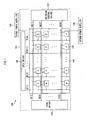
- an organic light emitting display is depicted as a block diagram.
- an organic light emitting display 100 includes a scan driver 110; a data driver 120; an emission control driver 130; an organic light emitting display panel 140 (hereinafter, referred to as panel 140); a first power supply 150; and a second power supply 160.
- the scan driver 110 can supply the panel 140 with a scan signal through a plurality of scan lines (S[1],...,S[N]) in sequence.
- the data driver 120 can supply the panel 140 with a data signal through a plurality of data lines (D[1],...,D[M]).
- the emission control driver 130 can supply the panel 140 with an emission control signal through a plurality of emission control lines (EM[1],...,EM[N]) in sequence.
- the panel 140 includes a plurality of scan lines (S[1],...,S[N]) arranged in a row direction, a plurality of emission control lines (EM[1],...,EM[M]) arranged in a row column direction, a plurality of data lines (D[1],...,D[M]) arranged in a column direction, and a pixel circuit (142, Pixel) which is defined by the scan lines (S[1],...,S[N]), the emission control lines (EM[1],...,EM[N]) and the data lines (D[1],...,D[M]).
- S[1],...,S[N] scan lines
- EM[1],...,EM[M] emission control lines
- D[1],...,D[M] data lines
- the pixel circuit (140, Pixel) can be formed at the pixel region which is defined by the scan lines and the data lines.
- the scan lines (S[1],...,S[N]) can be supplied with a scan signal from the scan driver 110
- the data lines (D[1],...,D[M]) can be supplied with a data signal from the data driver 120
- the emission control signal line (EM[1],...,EM[N]) can be supplied with an emission control signal from the emission control driver 130.
- the first power supply 150 and the second power supply 160 supply each pixel circuit 142 placed at the panel 140 with a first power supply voltage and a second power supply voltage.
- the scan driver 110, the data driver 120, the emission control driver 130, the panel 140, the first power supply 150 and the second power supply voltage driver 140 are formed on one substrate 102.
- the drivers and power supply voltage suppliers 110, 120, 130, 150 and 160 are formed on the same layer as the layer on which the scan lines (S[1],...,S[N]), the data lines (D[1],...,D[M])), the emission control lines (EM[1],...,EM[N]), and a transistor (not shown in drawings) of the pixel circuit 142 are formed.
- the drivers and the power supply voltage suppliers 110, 120, 130, 150 and 160 can be formed on another substrate (not shown in drawings), which can be coupled to the substrate 102.
- the drivers and the power supply voltage suppliers 110, 120, 130, 150 and 160 can be formed in a form such as TCP (Tape Carrier Package), FPC (Flexible Printed Circuit), TAB (Tape Automatic Bonding), COG (Chip On Glass), and the equivalent thereof, which couple the drivers and the suppliers to the substrate 102.
- TCP Transmission Carrier Package
- FPC Flexible Printed Circuit
- TAB Tape Automatic Bonding
- COG Chip On Glass
- the form and the location of the drivers and the suppliers 110, 120, 130, 150 and 160 are not limited.
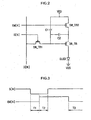
- FIG.2 a circuit diagram of a pixel circuit according to one embodiment of the organic light emitting display is depicted.
- a pixel circuit which will be described in the following means the pixel circuit formed on the panel 140 shown in FIG.1 .
- the pixel circuit of the organic light emitting display includes a scan line (S[N]); a data line (D[M]); an emission control line (EM[N]); a first power supply line (VDD); a second power supply line (VSS); a first switching transistor (SW_TR1); a second switching transistor (SW_TR2); a driving transistor (DR_TR); a first storage capacitor (C1); a second storage capacitor (C2); and an organic light emitting diode (OLED).
- S[N] scan line
- D[M] data line
- E[N] emission control line
- VDD first power supply line
- VSS second power supply line
- SW_TR1 first switching transistor
- SW_TR2 switching transistor
- DR_TR driving transistor
- C1 storage capacitor
- C2 organic light emitting diode
- the scan line (S[N]) supplies a control electrode of the first switching transistor (SW_TR1) with a scan signal which selects an organic light emitting diode (OLED) which will emit light.
- the scan line (S[N]) is coupled to the scan driver 110 (referring to FIG.1 ) which generates a scan signal.
- the data line (D[M]) supplies a second electrode of the first storage capacitor, a second electrode of the second storage capacitor, and a control electrode of the driving transistor (DR_TR) with a data signal (voltage) which is in proportion to the luminance.
- the data line (D[M]) is coupled to the data driver 120 (referring to FIG.1 ) which generates a data signal.
- the emission control line (EM[N]) supplies a control electrode of the second switching transistor (SW_TR2) with an emission control signal as it is coupled to the control electrode of the second switching transistor (SW_TR2).
- a first power supply voltage from the first power supply line (VDD) can be applied to a first electrode of the first storage capacitor (C1), a first electrode of the second storage capacitor (C2) and a first electrode of the first driving transistor (DR_TR).
- the emission control line (EM[N]) is coupled to the emission control driver 130 (referring to FIG.1 ) which generates an emission control signal.
- the first power supply line (VDD) supplies the organic light emitting diode (OLED) with a first power supply voltage.
- the first power supply line (VDD) is coupled to the first power supply 150 (referring to FIG.1 ) which supplies a first power supply voltage.
- the second power supply line supplies the organic light emitting diode (OLED) with a second power supply voltage.
- the second power supply line (VSS) is coupled to the second power supply 160 (referring to FIG.1 ) which supplies a second power supply voltage.
- the first power supply voltage can have a higher voltage level than that of the second power supply voltage in general.
- the second power supply voltage can use a ground voltage.
- the first switching transistor (SW_TR1) includes a first electrode (source or drain electrode) coupled to the data line (D[M]); a second electrode (source or drain electrode) coupled to a control electrode (gate electrode) of the driving transistor(DR_TR), a second electrode of the first storage capacitor (C1) and a second electrode of the second storage capacitor (C2); and a control electrode (gate electrode) coupled to the scan line (S[N]).
- the first switching transistor (SW_TR1) can be a P type channel transistor.
- the first switching transistor (SW_TR1) applies a data voltage to a second electrode of the first storage capacitor (C1), a second electrode of the second storage capacitor (C2) and a control electrode of the driving transistor (DR_TR) through the data line (D[M]).
- the driving transistor (DR_TR) includes a first electrode coupled to a first electrode of the second storage capacitor (C2) and a second electrode of the second switching transistor (SW_TR2); a second electrode coupled to an anode of the organic light emitting diode (OLED); and a control electrode coupled to the second electrode of the first switching transistor (SW_TR1), a second electrode of the first storage capacitor (C1) and a second electrode of the second storage capacitor (C2).
- the driving transistor can be a P type channel transistor.
- a method for driving the driving transistor (DR_TR), supplies an amount of current from the first power supply line (VDD) to the organic light emitting diode (OLED), once the driving transistor (DR_TR) is turned on by the signal of low level applied to the control electrode.
- a data signal is supplied to the storage capacitors, and is stored in the storage capacitors. Consequently, even if the electric connection with the data line (D[M]) is discontinued as the first switching transistor (SW_TR1) is turned off, a signal of low level can be applied to the control electrode of the driving transistor (DR_TR) continuously by the voltage charged in the storage capacitors.
- the driving transistor (DR_TR) can be, for example, any one selected from an amorphous silicon thin film transistor, a poly silicon thin film transistor, an organic thin film transistor, a nano thin film transistor, and the equivalent thereof.
- the material or the kind of the driving transistor is not limited.
- the driving transistor (DR_TR) is a poly silicon thin film transistor
- various crystallization methods such as an laser crystallization method (excimer laser annealing: ELA) using an excimer laser, a metal induced crystallization (MIC) using catalytic metals, a solid phase crystallization, a high pressure annealing wherein a crystallization is executed at a high temperature and a high humidity environment, and a sequential lateral solidification (SLS) using a mask in addition to a conventional laser crystallization.
- ELA laser crystallization method
- MIC metal induced crystallization
- SLS sequential lateral solidification
- the organic light emitting diode includes an anode coupled to the second electrode of the driving transistor (DR_TR) and a cathode coupled to the second power supply line (VSS).
- the organic light emitting diode (OLED) emits light in a luminance determined by the current controlled through the driving transistor (DR_TR) while the second switching transistor (SW_TR2) is turned on.
- the organic light emitting diode includes an emission layer (not shown).
- the emission layer can be, for example, any one selected from a fluorescent material, a phosphorescent material, a mixture of them, and the equivalent thereof. However, the material or the kind of the emission layer is not limited.
- the emission layer can be, for example, one selected from a red emitting material, a green emitting material, a blue emitting material, a mixture of them, and the equivalent of them.
- the material or the kind of the emission layer is not limited to this exemplary embodiment.
- the second switching transistor (SW_TR2) includes a first electrode coupled to the first power supply line (VDD) and a first electrode of the first storage capacitor (C1); a second electrode coupled to a first electrode of the second storage capacitor (C2) and the first electrode of the driving transistor (DR_TR); and a control electrode coupled to the emission control line (EM[N]).
- the second switching transistor (SW_TR2) in this embodiment is a P type channel transistor. Once the second switching transistor (SW_TR2) is turned on by the signal of low level applied to the control electrode through the emission control line (EM[N]), a current flows from the first power supply line (VDD) to the organic light emitting diode (OLED).
- the first storage capacitor (C1) includes a first electrode coupled to the first power supply line (VDD) and the first electrode of the second switching transistor (SW_TR2), and a second electrode coupled to a second electrode of the second storage capacitor (C2), the second electrode of the first switching transistor (SW_TR1) and the control electrode of the driving transistor (DR_TR).
- the second storage capacitor (C2) includes a first electrode coupled to the second electrode of the second switching transistor (SW_TR2) and the first electrode of the driving transistor (DR_TR), and a second electrode coupled to the second electrode of the first storage capacitor (C1), the second electrode of the first switching transistor (SW_TR1) and the control electrode of the driving transistor (DR_TR).
- the second storage capacitor (C2) maintains a data signal voltage and the threshold voltage of the driving transistor for a period.
- the voltage on the second storage capacitor (C2) controls a current, which is in proportion to the strength of a data signal, from the first power supply line to the organic light emitting diode. Consequently, the organic light emitting diode emits light.
- the compensation for IR-drop or the threshold voltage of the driving transistor which will be described in the following can be accomplished by controlling the capacitance ratio (C1:C2) of the first storage capacitor to the second storage capacitor.
- the first switching transistor (SW_TR1), the driving transistor (DR_TR) and the second switching transistor (SW_TR2) can, for example, be any one selected from a P type channel transistor and its equivalent.
- the kind of the transistor is not limited.
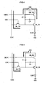
- one frame is classified into the first period, the second period and the third period. More particularly, one frame comprises a data writing period (T1), a period for storing the threshold voltage of the driving transistor (T2), and an emission period (T3).
- a data writing period (T1) a data writing period for storing the threshold voltage of the driving transistor (T2)
- an emission period (T3) Various ratios of the data writing period (T1) to the period for storing the threshold voltage of the driving transistor (T2) to the emission period (T3) can be formed.
- the data writing period (T1) and the period for storing the threshold voltage of the driving transistor (T2) are shorter than the emission period (T3).
- FIG.4 it is depicted how current flows through the pixel circuit shown in FIG.2 during the data writing period (T1). The operation of the pixel circuit mentioned above will be described with reference to the timing diagram of FIG.3 .
- the first switching transistor (SW_TR1) is turned on as a scan signal of low level is applied to the control electrode of the first switching transistor (SW_TR1). Then the second switching transistor (SW_TR2) is turned on as a signal of low level of the emission control line (EM[N]) is applied to the control electrode of the second switching transistor (SW_TR2).
- a data voltage (Vdata) of the data line (D[M]) is applied in a direction from the first electrode of the first switching transistor (SW_TR1) to the second electrode of the first switching transistor (SW_TR2). Consequently, the data voltage (Vdata) is applied to the second electrode of the first switching transistor (SW_TR1), the second electrode of the first storage capacitor (C1), the second electrode of the second storage capacitor (C2) and the control electrode of the driving transistor (DR_TR).
- SW_TR2 As the second switching transistor (SW_TR2) is turned on, a first power supply voltage from the first power supply line VDD is applied in a direction from the first electrode of the second switching transistor (SW_TR2) to the second electrode of the second switching transistor (SW_TR2). Consequently, the first power supply voltage is applied to the second electrode of the second switching transistor (SW_TR2), the first electrode of the second storage capacitor (C2) and the first electrode of the driving transistor (DR_TR).
- the first power supply voltage from the first power supply line (VDD) can also be applied to the first electrode of the first storage capacitor (Cl).
- the driving transistor (DR_TR) is turned on, thus current flows through the organic light emitting diode (OLED). Consequently, the organic light emitting diode (OLED) emits light.
- the voltage of Vdata is applied to the control electrode (gate electrode) of the driving transistor (DR_TR), the second electrode of the second storage capacitor (C2) and the second electrode of the first storage capacitor (C1).
- the voltage of VDD is applied to the first electrode (source electrode) of the driving transistor (DR_TR), the first electrode of the second storage capacitor (C2) and the first electrode of the first storage capacitor (C1). Accordingly, the voltage (VDD - Vdata), is stored in the storage capacitors.
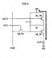
- FIG.5 it is depicted how a current flows through the pixel circuit shown in FIG.2 during storing the threshold voltage of the driving transistor (T2).
- T2 the threshold voltage of the driving transistor
- the first switching transistor (SW_TR1) is turned on as a scan signal of low level from the scan line (S[N]) is applied to the control electrode of the first switching transistor (SW_TR1), and the second switching transistor (SW_TR2) is turned off as a signal of high level from the emission control line (BM[N]) is applied to the control electrode of the second switching transistor (SW_TR2).
- a data voltage (Vdata) of the data line (D[M]) is applied from the first electrode of the first switching transistor (SW_TR1) to the second electrode of the first switching transistor (SW_TR1). consequently, the data voltage (Vdata) can be applied to the second electrode of the first switching transistor (SW-TP1), the second electrode of the first storage capacitor (C1), the second electrode of the second storage capacitor (C2) and the control electrode of the driving transistor (DR_TR).
- a first power supply voltage from the first power supply line (VDD) can be applied to the first electrode of the first storage capacitor (C1).
- the driving transistor (DR_TR) is turned on, thus current is applied to the organic light emitting diode (OLED). Consequently, the organic light emitting diode (OLED) emits light.
- the voltage of Vdata is applied to the control electrode (gate electrode) of the driving transistor (DR_TR), the second electrode of the second storage capacitor (C2) and the second electrode of the first storage capacitor (C1).
- the voltage of VDD is applied to the first electrode of the first storage capacitor (C1). Accordingly, the voltage (VDD-Vdata) is stored in the first storage capacitor (C1).
- the first switching transistor (SW_TR1) is turned off as a signal of high level is applied from the scan line (S[N]) to the control electrode of the first switching transistor (SW_TR1)
- the second switching transistor (SW_TR2) is turned off as a signal of high level is applied from the emission control line (EM[N]) to the control electrode of the second switching transistor (SW_TR2).
- the voltage stored in the storage capacitors during the second period (T2) is maintained without any changes.
- FIG.6 it is depicted how a current flows through the pixel circuit shown in FIG.2 during the emission period (T3).
- T3 emission period
- the first switching transistor (SW_TR1) is turned off as a signal of high level from the scan line (S[N]) is applied to the control electrode of the first switching transistor (SW_TR1), and the second switching transistor (SW_TR2) is turned on as a signal of low level of the emission control line (EM[N]) is applied to the control electrode of the second switching transistor (SW_TR2).
- a first power supply voltage from the first power supply line (VDD) is applied from the first electrode of the second switching transistor (SW_TR2) to the second electrode of the second switching transistor (SW_TR2). Consequently, the first power supply voltage can be applied to the first electrode (source electrode) of the driving transistor (DR_TR).
- a current from the first power supply line (VDD) can flow toward the second power supply line (VSS) through the organic light emitting diode (OLED) during the emission period (T3). Accordingly, the organic light emitting diode can emit light.
- the voltage (Vs) of the first electrode (source electrode) of the driving transistor (DR_TR) becomes VDD.
- the voltage (Vg) of the control electrode (gate electrode) of the driving transistor (DR_TR) and the voltage difference (Vsg) between the source electrode and the gate electrode of the driving transistor (DR_TR) can be calculated from the Formula 1 in the following.
- V g V data + C ⁇ 2 C ⁇ 1 + C ⁇ 2 * VDD - V data - Vth
- V s VDD
- V sg V s - V g
- V Sg VDD - V data + C ⁇ 2 C ⁇ 1 + C ⁇ 2 * VDD - V data - Vth
- I OLED ⁇ 2 * V Sg - Vth 2 That is to say, the threshold voltage (Vth) of the driving transistor (DR_TR) is stored in the second storage capacitor (C2) during the second period (T2). Subsequently, data is expressed by the data voltage (Vdata) and the ratio of C1 to C2 during the emission period (T3).
- C2 is set to have a larger value than that of C1 (that is, C2>>C1)
- C2 divided by C1 added to C2 (C2/(C1+C2)) can be approximately 1.
- Vth is left in Vsg in the Formula 1 described above.
- Vsg is substituted with Vth in Formula 2
- the threshold voltage (Vth) of the driving transistor can be compensated to a current flowing through the organic light emitting diode (OLED).
- Vsg of the driving transistor (DR_TR) is Vth. Therefore, as shown in Formula 2, no data voltage (Vdata) appears in the Formula of the organic light emitting diode. Accordingly, the current wanted according to a data voltage (Vdata) cannot be generated. Therefore, the data range expands infinitely. Nevertheless, if C1 is set to have a much larger value than that of C2, then C2 divided by C1 added to C2 (C2/(C1+C2)) becomes 0 approximately. Consequently, Vsg in Formula 1 becomes VDD-Vdata.
- the current wanted can be generated according to a data voltage (Vdata).
- Vdata a data voltage
- the compensation for the threshold voltage (Vth) of the driving transistor (DR_TR) or the compensation for IR-drop of the first power supply line (VDD) cannot be accomplished properly.
- the threshold voltage (Vth) of the driving transistor (DR_TR) and IR-drop by the first power supply line (VDD) can be compensated by controlling the ratio of C1 to C2 properly.
- Vsg becomes VDD - Vdata - 0.5 VDD + 0.5Vdata + 0.5Vth. Consequently, the data range is increased twofold, and the influence of the threshold voltage (Vth) of the driving transistor (DR_TR) and IR-drop of the first power supply line (VDD) can be reduced to half. That is, the influence of the threshold voltage (Vth) of the driving transistor (DR_TR) and IR-drop of the first power supply line (VDD) can be minimized by determining C2 to have a larger value than that of C1.
- a leakage current can flow through the path.
- the leakage current off current of the driving transistor
- improper emission can be generated by the leakage current which flows into the organic light emitting diode (OLED).
- OLED organic light emitting diode
- the leakage characteristics of driving transistors in a panel differ from one another, although a black image should be expressed, some pixels which have large leakage characteristics can emit some light.
- the improper emission described above can be reduced by having the driving transistor undergo a reverse aging because the reverse aging can reduce the leakage current of the driving transistor.
- the pixel circuit of FIG. 2 has essentially no leakage. Consequently, the reverse aging for the driving transistor described above is not required.
- the data writing period (T1) and the period for storing the threshold voltage of the driving transistor (T2) should be shorter than the emission period (T3) so that the time during which the organic light emitting diode (OLED) emits light can become maximized.
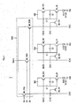
- RGB pixel circuits and a demux are coupled according to one embodiment.
- the demux may have a layout structure which corresponds to each RGB data signal of the data driver of the organic light emitting display.
- the demux includes a plurality of data supplying switching elements which are connected in common to the output line of the data driver, and the respective data supplying switching elements are coupled to separate data lines. Therefore, the demux supplies each data line with a data signal in sequence through the operation of the data supplying switching elements.
- RGB means red (Red, R), green (Green, G) and blue (Blue, B).
- R red
- Green Green
- B blue
- a data signal can be applied to pixel circuits by using a plurality of demuxes, the number of demuxes used is not limited.
- each red data line, green data line and blue data line is coupled to the data line (D[M]) of the respective pixel circuits.
- each RGB data line is coupled to a RGB switching transistor (SW_TR3).
- the RGB switching transistor consists of a red data line switching transistor (SW_TR3R), a green data line switching transistor (SW_TR3G) and a blue data line switching transistor (SW_TR3G).
- RGB control signals can be applied to a control electrode) of the RGB switching transistors through RGB control lines (CR, CG and CB) respectively.
- RGB switching transistor Once the RGB switching transistor is turned on by the RGB control signals (CR, CG and CB), a proper data signal (voltage) can be applied to each RGB pixel circuit from the data driver through the demux.
- the RGB switching transistors can be P type channel transistors, but the kind of the RGB switching transistor is not limited.
- FIG.8 and FIG.9 a driving timing diagram of the RGB pixel circuits of FIG.7 is depicted.
- each first switching transistor (SW_TR1) of the RGB pixel circuits is turned on.
- each second switching transistor (SW_TR2) of the RGB pixel circuits is turned on.
- the RGB switching transistors (SW_TR3) are turned on by applying a signal of low level through the RGB control lines (CR, CG and CB) during a period during which the scan signal and the emission control signal are low level. Consequently, the RGB data signal can be applied.
- the RGB switching transistors (SW_TR3) are turned on when a signal of low level is applied to them, as described above.
- the RGB switching transistors (SW_TR3) are turned on as a signal of high level is applied to them. Consequently, the driving timing diagrams can be different.
- the kind of the transistor and the driving timing diagram are not limited to the specific examples described.
- each first switching transistor (SW_TR1) of the RGB pixel circuits is turned off.
- each second switching transistor (SW_TR2) of the RGB pixel circuits is turned on.
- the RGB switching transistors (SW_TR3) are turned on by applying a signal of low level through the RGB control lines (CR, CG and CB) during the period during which the scan signal is high level and the emission control signal is low level. Consequently, the RGB data signal can be applied.
- the first switching transistor (SW_TR1) When a scan signal of high level is applied to the control electrode of the first switching transistor (SW_TR1) of the pixel circuit, the first switching transistor (SW_TR1) is turned off. Consequently, during the period which a turn-off scan signal is applied, the RGB data signal is not applied to the storage capacitor of the pixel circuit.
- the first switching transistor (SW_TR1) is turned on as a turn-on scan signal is applied to the control electrode of the first switching transistor (SW_TR1) after the data signal (voltage) is charged by a parasitic capacitor (Cd) formed by the data lines (D[M]), the data signals charged in the parasitic capacitor (Cd) is applied through the first switching transistor (SW_TR1).
- the capacitance of the parasitic capacitor (Cd) can be larger than that of the first storage capacitor (C1) and the second storage capacitor (C2) included in the pixel circuit.
- the RGB switching transistors (SW_TR3) are turned on when a signal of low level is applied to them.
- the RGB switching transistors (SW_TR3) are turned on as a signal of high level is applied to them. Consequently, the driving timing diagrams can be different.
- the kind of the transistor and the driving timing diagram is not limited to those disclosed in the specification.
- the RGB switching transistors (SW_TR3) are turned on by applying a signal of low level through the RGB control lines (CR, CG and CB) during the period which a signal of low level is applied from the emission control line (EM[N]), regardless of whether a high level or low level is applied.from the scan line (S[N]).
- the storage capacitors which have stored a previous data voltage, can be initialized as they are coupled to the first power supply line (VDD).
- the storage capacitors can be coupled to the first power supply line (VDD) as the second switching transistors (SW_TR2) of the pixel circuits are turned on by a signal of low level applied from the emission control line (EM[N]). Consequently, proper data can be written on the storage capacitors by applying new RGB data signals after the storage capacitors are initialized.
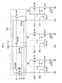
- FIG.10 depicts how the RGB pixel circuits and the demux may be coupled.
- the demux 1000 has a layout structure corresponding to each RGB data signal of the data driver of the organic light emitting display, and it is similar to the demux shown in FIG.7 .
- the Demux 1000 also includes an initializing power supply voltage line (Vrst) and an initializing switching transistor (SW_TR4) which couples the initialing power supply voltage line (Vrst) to a RGB data voltage line.
- Vrst initializing power supply voltage line
- SW_TR4 initializing switching transistor
- pixel circuits are coupled to the demux 1000 in FIG.10 , however, the number of pixel circuits coupled to the demux is not limited.
- a data signal can be applied to the pixel circuits by using a plurality of demuxes, and the number of demuxes used is not limited.
- each red data line, green data line and blue data line is coupled to the data line (D[M]) of the respective pixel circuits.
- each RGB data line is coupled to RGB switching transistor (SW_TR3).
- the RGB switching transistor comprises a red data line switching transistor (SW_TR3R), a green data line switching transistor (SW_TR3G) and a blue data line switching transistor (SW_TR3B).
- RGB control signals can be applied to a control electrode of the RGB switching transistors through RGB control lines (CR, CG and CB) respectively.
- RGB switching transistor Once the RGB switching transistor is turned on by the respective RGB control signals (CR, CG and CB), a proper data signal (voltage) from the data driver can be applied to the respective RGB pixel circuit through the demux.
- the initializing power supply voltage line (Vrst) is coupled to the respective RGB data line through the initializing switching transistor (SW_TR4).
- SW_TR4G, SW_TR4R and SW_TR4B initializing switching transistors
- an initializing power supply voltage can be applied to each RGB data line from the initializing power supply voltage line (Vrst).
- the initializing power supply voltage is applied, the previous data voltages applied to the RGB data lines are initialized. Consequently, new RGB data signals (voltages) can be applied.
- the RGB switching transistor and the initializing power supply voltage can be a P type channel transistor, however, the kind of the transistor is not limited.
- a thin film transistor can be used as the RGB switching transistor (SW_TR3) shown in FIG.7 and the initializing switching transistor (SW_TR4) shown in FIG.10 .
- a crystallization method for the thin film transistor a laser crystallization method (ELA) using an excimer laser, a metal induced crystallization (MIC) using a catalytic metal and a solid phase crystallization can be used.
- MIC metal induced crystallization
- HPA high pressure annealing
- the laser crystallization method is a widely used crystallization method in which a thin film transistor is crystallized into poly silicon. Not only can the method directly use existing crystallization processes for poly silicon liquid crystal display devices, but also the process is simple, and the technology of the process has been completely established.
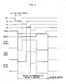
- FIG.11 a driving timing diagram of the RGB pixel circuits shown in FIG.10 is depicted.
- the RGB switching transistors SW_TR3R, SW_TR3G and SW_TR3B can be turned on as a signal of low level is applied through the RGB control signal line.
- the RGB control signal is applied in order of a green, red and blue control signals. Consequently, the RGB data voltage is applied to the respective green, red and blue pixel circuits in sequence.
- a green organic light emitting diode emits light as a current flows through the green organic light emitting diode (OLED Green) from the period during which a green emission control signal is applied to the period during which an emission control signal of high level from the emission control line (EM[N]) is applied.
- a red organic light emitting diode (OLED Red) emits light as a current flows through the red organic light emitting diode (OLED Red) from the period during which a red emission control signal is applied to the period during which an emission control signal of high level from the emission control line (EM[N]) is applied.
- a blue organic light remitting diode (OLED Blue) emits light as a current flows through the blue organic light emitting diode (OLED Blue) from the period during which a blue emission control signal is applied to the period during which an emission control signal of high level from the emission control line (EM[N]) is applied.
- a current flows through a green organic light emitting diode for the longest time, and a red green organic light emitting diode is next, and a blue organic light emitting diode is the shortest.
- the reason why the time for compensating the white balance is arranged in order of green, red and blue is that a green OLED has a higher luminous efficiency than red and green OLEDs.
- a current flows through a green organic light emitting diode of the best luminous efficiency for the longest time during the non-emission period (the period for compensating the white balance).
- the period for compensating the white balance is performed. Therefore, a uniform luminance can be accomplished.
- a larger current flows through the organic light emitting diode than a current flowing during the emission period.
- the period for compensating the white balance can be shorter than the emission period.
- the organic light emitting display can divide a period for displaying one frame into the first period (T1), the second period (T2) and the third period (T3).
- Each period consists of a data writing period (T1), a period for storing the threshold voltage of the driving transistor (T2) and an emission period (T3).
- the uniformity of the luminance can be improved by compensating the threshold voltage (Vth) and controlling the ratio (C1:C2) of a first storage capacitor to a second storage capacitor properly. Furthermore, IR-drop by a first power supply line (VDD) can be improved by controlling the capacitance ratio of the first storage capacitor to the second storage capacitor.
- an improper emission of the organic light emitting diode can be suppressed because an electric connection through which a leakage current can flow from the control electrode of the driving transistor to the negative power supply voltage does not exist.
- RGB data signal In the case of a driving method an RGB data signal is applied by using the demux, the RGB data signal is applied during a period which an emission control signal is turned on regardless of the scan signal being turned on or off. Consequently, the RGB data can be stored in each storage capacitor properly.
- a new RGB data signal can be stored in the storage capacitors properly because the respective storage capacitors are initialized by the first power supply voltage of the first power supply line, before the RGB data is applied to each storage capacitor of the respective pixel circuits.
- an RGB data signal is applied using the demux during the non-emission period (the period for compensating the white balance).
- a current should flow through the light emitting diode of the longest lifetime for the longest time.
- the period for compensating the white balance is performed. Consequently, the lifetime of uniform luminance level can be extended. Accordingly, the color wanted can be reproduced because the white balance is maintained as time goes by, because the period for compensating the white balance is performed.
Applications Claiming Priority (1)
| Application Number | Priority Date | Filing Date | Title |
|---|---|---|---|
| KR1020070004860A KR100833760B1 (ko) | 2007-01-16 | 2007-01-16 | 유기 전계 발광 표시 장치 |
Publications (3)
| Publication Number | Publication Date |
|---|---|
| EP1947633A2 EP1947633A2 (en) | 2008-07-23 |
| EP1947633A3 EP1947633A3 (en) | 2010-06-02 |
| EP1947633B1 true EP1947633B1 (en) | 2015-12-02 |
Family
ID=39387356
Family Applications (1)
| Application Number | Title | Priority Date | Filing Date |
|---|---|---|---|
| EP08250060.4A Active EP1947633B1 (en) | 2007-01-16 | 2008-01-08 | Organic light emitting display |
Country Status (5)
| Country | Link |
|---|---|
| US (1) | US8232933B2 (ja) |
| EP (1) | EP1947633B1 (ja) |
| JP (1) | JP4932624B2 (ja) |
| KR (1) | KR100833760B1 (ja) |
| CN (1) | CN101226719B (ja) |
Families Citing this family (34)
| Publication number | Priority date | Publication date | Assignee | Title |
|---|---|---|---|---|
| KR100882907B1 (ko) * | 2007-06-21 | 2009-02-10 | 삼성모바일디스플레이주식회사 | 유기전계발광표시장치 |
| KR100867926B1 (ko) * | 2007-06-21 | 2008-11-10 | 삼성에스디아이 주식회사 | 유기전계발광표시장치 및 그의 제조 방법 |
| JP5063433B2 (ja) * | 2008-03-26 | 2012-10-31 | 富士フイルム株式会社 | 表示装置 |
| KR100936883B1 (ko) * | 2008-06-17 | 2010-01-14 | 삼성모바일디스플레이주식회사 | 화소 및 이를 이용한 유기전계발광 표시장치 |
| RU2479047C2 (ru) * | 2008-09-10 | 2013-04-10 | Шарп Кабусики Кайся | Дисплейное устройство и способ для его возбуждения |
| KR100986896B1 (ko) | 2008-12-05 | 2010-10-08 | 삼성모바일디스플레이주식회사 | 유기전계발광 표시장치 및 그의 구동방법 |
| KR101484951B1 (ko) | 2008-12-17 | 2015-01-21 | 엘지디스플레이 주식회사 | 유기전계 발광 디스플레이 장치 |
| KR101056240B1 (ko) | 2009-03-02 | 2011-08-11 | 삼성모바일디스플레이주식회사 | 유기전계발광 표시장치 |
| JP5218269B2 (ja) * | 2009-05-13 | 2013-06-26 | ソニー株式会社 | 表示装置および駆動制御方法 |
| JP5299126B2 (ja) | 2009-07-01 | 2013-09-25 | セイコーエプソン株式会社 | 発光装置および電子機器、並びに画素回路の駆動方法。 |
| KR101082283B1 (ko) * | 2009-09-02 | 2011-11-09 | 삼성모바일디스플레이주식회사 | 유기전계발광 표시장치 및 그의 구동방법 |
| KR101034734B1 (ko) * | 2009-10-09 | 2011-05-17 | 삼성모바일디스플레이주식회사 | 화소 및 이를 이용한 유기전계발광 표시장치 |
| KR101056293B1 (ko) * | 2009-10-26 | 2011-08-11 | 삼성모바일디스플레이주식회사 | 화소 및 이를 이용한 유기전계발광 표시장치 |
| JP5482393B2 (ja) * | 2010-04-08 | 2014-05-07 | ソニー株式会社 | 表示装置、表示装置のレイアウト方法、及び、電子機器 |
| KR101681097B1 (ko) * | 2010-07-27 | 2016-12-02 | 삼성디스플레이 주식회사 | 화소 및 이를 이용한 유기전계발광 표시장치 |
| CN102958239A (zh) * | 2011-08-31 | 2013-03-06 | 鸿富锦精密工业(深圳)有限公司 | 硬盘指示灯电路 |
| KR101960458B1 (ko) * | 2012-09-18 | 2019-03-21 | 삼성디스플레이 주식회사 | 유기 발광 표시 장치 |
| KR101970574B1 (ko) * | 2012-12-28 | 2019-08-27 | 엘지디스플레이 주식회사 | Oled 표시 장치 |
| KR102278599B1 (ko) * | 2014-11-19 | 2021-07-16 | 삼성디스플레이 주식회사 | 유기 발광 표시 장치 및 이의 구동 방법 |
| CN104867452A (zh) * | 2015-06-08 | 2015-08-26 | 深圳市华星光电技术有限公司 | 信号分离器及amoled显示装置 |
| CN105609048B (zh) * | 2016-01-04 | 2018-06-05 | 京东方科技集团股份有限公司 | 一种像素补偿电路及其驱动方法、显示装置 |
| KR102648975B1 (ko) * | 2016-11-30 | 2024-03-19 | 엘지디스플레이 주식회사 | 유기발광 표시장치 및 그의 구동특성 보상방법 |
| JP6914732B2 (ja) * | 2017-05-29 | 2021-08-04 | キヤノン株式会社 | 発光装置及び撮像装置 |
| KR102312348B1 (ko) * | 2017-06-30 | 2021-10-13 | 엘지디스플레이 주식회사 | 표시패널과 이를 이용한 전계 발광 표시장치 |
| KR102416435B1 (ko) * | 2017-08-28 | 2022-07-04 | 삼성디스플레이 주식회사 | 표시장치 |
| CN110010072A (zh) * | 2018-01-05 | 2019-07-12 | 京东方科技集团股份有限公司 | 像素电路及其驱动方法、显示装置 |
| CN108877668B (zh) * | 2018-07-27 | 2021-01-22 | 京东方科技集团股份有限公司 | 一种像素电路、其驱动方法及显示面板 |
| WO2020026307A1 (ja) * | 2018-07-30 | 2020-02-06 | シャープ株式会社 | 表示デバイス |
| TWI717855B (zh) * | 2019-10-05 | 2021-02-01 | 友達光電股份有限公司 | 畫素電路及顯示裝置 |
| US11238784B1 (en) * | 2020-08-27 | 2022-02-01 | Wuhan China Star Optoelectronics Technology Co., Ltd. | Pixel circuit and display panel |
| KR20220069201A (ko) | 2020-11-19 | 2022-05-27 | 삼성디스플레이 주식회사 | 영상 프로세서, 그것을 포함하는 표시 장치 및 표시 장치의 동작 방법 |
| KR20230064708A (ko) * | 2021-11-03 | 2023-05-11 | 삼성디스플레이 주식회사 | 화소 및 이를 포함하는 표시 장치 |
| KR20230110412A (ko) | 2022-01-14 | 2023-07-24 | 삼성디스플레이 주식회사 | 화소 및 이를 포함하는 표시 장치 |
| US20230317012A1 (en) * | 2022-03-31 | 2023-10-05 | Meta Platforms Technologies, Llc | Self-compensation of driving transistor threshold voltage using body effect |
Citations (1)
| Publication number | Priority date | Publication date | Assignee | Title |
|---|---|---|---|---|
| EP1923857A2 (en) * | 2006-11-14 | 2008-05-21 | Samsung SDI Co., Ltd. | Pixel, organic light emitting display device and driving method thereof |
Family Cites Families (33)
| Publication number | Priority date | Publication date | Assignee | Title |
|---|---|---|---|---|
| US1234567A (en) * | 1915-09-14 | 1917-07-24 | Edward J Quigley | Soft collar. |
| US6636191B2 (en) * | 2000-02-22 | 2003-10-21 | Eastman Kodak Company | Emissive display with improved persistence |
| US7541184B2 (en) * | 2000-02-24 | 2009-06-02 | Invitrogen Corporation | Activation and expansion of cells |
| JP3800404B2 (ja) * | 2001-12-19 | 2006-07-26 | 株式会社日立製作所 | 画像表示装置 |
| KR100489272B1 (ko) | 2002-07-08 | 2005-05-17 | 엘지.필립스 엘시디 주식회사 | 유기 전계발광소자 및 그의 구동방법 |
| JP4230746B2 (ja) * | 2002-09-30 | 2009-02-25 | パイオニア株式会社 | 表示装置及び表示パネルの駆動方法 |
| JP2004138773A (ja) * | 2002-10-17 | 2004-05-13 | Tohoku Pioneer Corp | アクティブ型発光表示装置 |
| JP2004151194A (ja) * | 2002-10-29 | 2004-05-27 | Tohoku Pioneer Corp | アクティブ型発光表示パネルの駆動装置 |
| JP2006516745A (ja) | 2003-01-24 | 2006-07-06 | コーニンクレッカ フィリップス エレクトロニクス エヌ ヴィ | アクティブマトリクス表示装置 |
| US6975293B2 (en) * | 2003-01-31 | 2005-12-13 | Faraday Technology Corp. | Active matrix LED display driving circuit |
| KR100502912B1 (ko) * | 2003-04-01 | 2005-07-21 | 삼성에스디아이 주식회사 | 발광 표시 장치 및 그 표시 패널과 구동 방법 |
| KR100497246B1 (ko) * | 2003-04-01 | 2005-06-23 | 삼성에스디아이 주식회사 | 발광 표시 장치 및 그 표시 패널과 구동 방법 |
| JP4467910B2 (ja) * | 2003-05-16 | 2010-05-26 | 東芝モバイルディスプレイ株式会社 | アクティブマトリクス型表示装置 |
| JP4360121B2 (ja) * | 2003-05-23 | 2009-11-11 | ソニー株式会社 | 画素回路、表示装置、および画素回路の駆動方法 |
| KR100515318B1 (ko) | 2003-07-30 | 2005-09-15 | 삼성에스디아이 주식회사 | 표시 장치와 그 구동 방법 |
| KR100686335B1 (ko) | 2003-11-14 | 2007-02-22 | 삼성에스디아이 주식회사 | 표시장치 및 그의 구동방법 |
| KR100536235B1 (ko) * | 2003-11-24 | 2005-12-12 | 삼성에스디아이 주식회사 | 화상 표시 장치 및 그 구동 방법 |
| JP4600723B2 (ja) * | 2003-12-26 | 2010-12-15 | ソニー株式会社 | 画素回路及び表示装置とこれらの駆動方法 |
| US20050275352A1 (en) * | 2004-06-14 | 2005-12-15 | Au Optronics Corporation. | Redundant storage capacitor and method for repairing OLED pixels and driving circuits |
| KR100581810B1 (ko) | 2004-08-25 | 2006-05-23 | 삼성에스디아이 주식회사 | 발광 표시장치와 그의 구동방법 |
| KR100673759B1 (ko) * | 2004-08-30 | 2007-01-24 | 삼성에스디아이 주식회사 | 발광 표시장치 |
| US20060085063A1 (en) * | 2004-10-15 | 2006-04-20 | Shastri V P | Nano- and micro-scale engineering of polymeric scaffolds for vascular tissue engineering |
| KR100592646B1 (ko) | 2004-11-08 | 2006-06-26 | 삼성에스디아이 주식회사 | 발광 표시장치 및 그의 구동방법 |
| KR100688800B1 (ko) | 2004-11-17 | 2007-03-02 | 삼성에스디아이 주식회사 | 발광 표시장치와 그의 구동방법 |
| KR100604060B1 (ko) | 2004-12-08 | 2006-07-24 | 삼성에스디아이 주식회사 | 발광 표시장치와 그의 구동방법 |
| KR101152120B1 (ko) * | 2005-03-16 | 2012-06-15 | 삼성전자주식회사 | 표시 장치 및 그 구동 방법 |
| KR20060109343A (ko) | 2005-04-15 | 2006-10-19 | 세이코 엡슨 가부시키가이샤 | 전자 회로, 그 구동 방법, 전기 광학 장치, 및 전자 기기 |
| KR101160830B1 (ko) * | 2005-04-21 | 2012-06-29 | 삼성전자주식회사 | 표시 장치 및 그 구동 방법 |
| KR20070002189A (ko) * | 2005-06-30 | 2007-01-05 | 엘지.필립스 엘시디 주식회사 | 발광표시장치 |
| TWI317925B (en) * | 2005-08-19 | 2009-12-01 | Toppoly Optoelectronics Corp | An active matrix organic light emitting diodes pixel circuit |
| KR101202040B1 (ko) * | 2006-06-30 | 2012-11-16 | 엘지디스플레이 주식회사 | 유기발광다이오드 표시소자 및 그 구동방법 |
| KR100821055B1 (ko) * | 2006-12-27 | 2008-04-08 | 삼성에스디아이 주식회사 | 유기전계발광 표시장치와 그의 구동방법 |
| CN101374298A (zh) * | 2007-08-24 | 2009-02-25 | 深圳富泰宏精密工业有限公司 | 资料自动分类系统及方法 |
-
2007
- 2007-01-16 KR KR1020070004860A patent/KR100833760B1/ko active IP Right Grant
- 2007-07-09 JP JP2007179978A patent/JP4932624B2/ja active Active
- 2007-12-27 US US12/005,699 patent/US8232933B2/en not_active Expired - Fee Related
-
2008
- 2008-01-08 EP EP08250060.4A patent/EP1947633B1/en active Active
- 2008-01-16 CN CN2008100027403A patent/CN101226719B/zh active Active
Patent Citations (1)
| Publication number | Priority date | Publication date | Assignee | Title |
|---|---|---|---|---|
| EP1923857A2 (en) * | 2006-11-14 | 2008-05-21 | Samsung SDI Co., Ltd. | Pixel, organic light emitting display device and driving method thereof |
Also Published As
| Publication number | Publication date |
|---|---|
| EP1947633A2 (en) | 2008-07-23 |
| CN101226719A (zh) | 2008-07-23 |
| JP2008176272A (ja) | 2008-07-31 |
| CN101226719B (zh) | 2010-11-03 |
| JP4932624B2 (ja) | 2012-05-16 |
| EP1947633A3 (en) | 2010-06-02 |
| US8232933B2 (en) | 2012-07-31 |
| US20080170010A1 (en) | 2008-07-17 |
| KR100833760B1 (ko) | 2008-05-29 |
Similar Documents
| Publication | Publication Date | Title |
|---|---|---|
| EP1947633B1 (en) | Organic light emitting display | |
| US8274452B2 (en) | Organic light emitting display having compensation for transistor threshold variation | |
| US9741292B2 (en) | Method and system for programming and driving active matrix light emitting device pixel having a controllable supply voltage | |
| US8149187B2 (en) | Organic light emitting display | |
| US10283045B2 (en) | Display device | |
| EP1884912B1 (en) | Light emitting display | |
| JP4177823B2 (ja) | 発光表示装置とその表示パネル,及び駆動方法 | |
| US7609234B2 (en) | Pixel circuit and driving method for active matrix organic light-emitting diodes, and display using the same | |
| US8237637B2 (en) | Organic light emitting display and driving method thereof | |
| US8994626B2 (en) | Display and method for manufacturing display | |
| KR100570774B1 (ko) | 발광표시 장치의 표시 데이터용 메모리 관리 방법 | |
| KR100530559B1 (ko) | 표시 구동 회로 | |
| US20090140957A1 (en) | Pixel and organic light emitting display using the same | |
| KR20080067489A (ko) | 유기 전계 발광 표시 장치 | |
| KR20050092207A (ko) | 발광 표시 장치 및 그 구동 방법 | |
| US20050140599A1 (en) | Electro-luminescence display device and driving apparatus thereof | |
| CN117441202A (zh) | 显示装置 | |
| KR20050078823A (ko) | 일렉트로-루미네센스 표시장치와 그의 구동방법 |
Legal Events
| Date | Code | Title | Description |
|---|---|---|---|
| PUAI | Public reference made under article 153(3) epc to a published international application that has entered the european phase |
Free format text: ORIGINAL CODE: 0009012 |
|
| 17P | Request for examination filed |
Effective date: 20080115 |
|
| AK | Designated contracting states |
Kind code of ref document: A2 Designated state(s): AT BE BG CH CY CZ DE DK EE ES FI FR GB GR HR HU IE IS IT LI LT LU LV MC MT NL NO PL PT RO SE SI SK TR |
|
| AX | Request for extension of the european patent |
Extension state: AL BA MK RS |
|
| RAP1 | Party data changed (applicant data changed or rights of an application transferred) |
Owner name: SAMSUNG MOBILE DISPLAY CO., LTD. |
|
| PUAL | Search report despatched |
Free format text: ORIGINAL CODE: 0009013 |
|
| AK | Designated contracting states |
Kind code of ref document: A3 Designated state(s): AT BE BG CH CY CZ DE DK EE ES FI FR GB GR HR HU IE IS IT LI LT LU LV MC MT NL NO PL PT RO SE SI SK TR |
|
| AX | Request for extension of the european patent |
Extension state: AL BA MK RS |
|
| AKX | Designation fees paid |
Designated state(s): DE FR GB HU |
|
| 17Q | First examination report despatched |
Effective date: 20110418 |
|
| RAP1 | Party data changed (applicant data changed or rights of an application transferred) |
Owner name: SAMSUNG DISPLAY CO., LTD. |
|
| GRAP | Despatch of communication of intention to grant a patent |
Free format text: ORIGINAL CODE: EPIDOSNIGR1 |
|
| INTG | Intention to grant announced |
Effective date: 20150316 |
|
| GRAP | Despatch of communication of intention to grant a patent |
Free format text: ORIGINAL CODE: EPIDOSNIGR1 |
|
| INTG | Intention to grant announced |
Effective date: 20150604 |
|
| INTG | Intention to grant announced |
Effective date: 20150608 |
|
| RAP1 | Party data changed (applicant data changed or rights of an application transferred) |
Owner name: SAMSUNG DISPLAY CO., LTD. |
|
| GRAS | Grant fee paid |
Free format text: ORIGINAL CODE: EPIDOSNIGR3 |
|
| GRAA | (expected) grant |
Free format text: ORIGINAL CODE: 0009210 |
|
| AK | Designated contracting states |
Kind code of ref document: B1 Designated state(s): DE FR GB HU |
|
| REG | Reference to a national code |
Ref country code: GB Ref legal event code: FG4D |
|
| REG | Reference to a national code |
Ref country code: FR Ref legal event code: PLFP Year of fee payment: 9 |
|
| REG | Reference to a national code |
Ref country code: DE Ref legal event code: R096 Ref document number: 602008041375 Country of ref document: DE |
|
| REG | Reference to a national code |
Ref country code: DE Ref legal event code: R097 Ref document number: 602008041375 Country of ref document: DE |
|
| PLBE | No opposition filed within time limit |
Free format text: ORIGINAL CODE: 0009261 |
|
| STAA | Information on the status of an ep patent application or granted ep patent |
Free format text: STATUS: NO OPPOSITION FILED WITHIN TIME LIMIT |
|
| 26N | No opposition filed |
Effective date: 20160905 |
|
| REG | Reference to a national code |
Ref country code: FR Ref legal event code: PLFP Year of fee payment: 10 |
|
| REG | Reference to a national code |
Ref country code: FR Ref legal event code: PLFP Year of fee payment: 11 |
|
| PG25 | Lapsed in a contracting state [announced via postgrant information from national office to epo] |
Ref country code: HU Free format text: LAPSE BECAUSE OF FAILURE TO SUBMIT A TRANSLATION OF THE DESCRIPTION OR TO PAY THE FEE WITHIN THE PRESCRIBED TIME-LIMIT; INVALID AB INITIO Effective date: 20080108 |
|
| PGFP | Annual fee paid to national office [announced via postgrant information from national office to epo] |
Ref country code: DE Payment date: 20221220 Year of fee payment: 16 |
|
| P01 | Opt-out of the competence of the unified patent court (upc) registered |
Effective date: 20230515 |
|
| PGFP | Annual fee paid to national office [announced via postgrant information from national office to epo] |
Ref country code: GB Payment date: 20231220 Year of fee payment: 17 |
|
| PGFP | Annual fee paid to national office [announced via postgrant information from national office to epo] |
Ref country code: FR Payment date: 20231222 Year of fee payment: 17 |