EP1944649A1 - Electrophoretic display apparatus and manufacturing method thereof - Google Patents
Electrophoretic display apparatus and manufacturing method thereof Download PDFInfo
- Publication number
- EP1944649A1 EP1944649A1 EP07252532A EP07252532A EP1944649A1 EP 1944649 A1 EP1944649 A1 EP 1944649A1 EP 07252532 A EP07252532 A EP 07252532A EP 07252532 A EP07252532 A EP 07252532A EP 1944649 A1 EP1944649 A1 EP 1944649A1
- Authority
- EP
- European Patent Office
- Prior art keywords
- substrate
- electrophoretic
- display apparatus
- color filter
- electrophoretic display
- Prior art date
- Legal status (The legal status is an assumption and is not a legal conclusion. Google has not performed a legal analysis and makes no representation as to the accuracy of the status listed.)
- Withdrawn
Links
Images


Classifications
-
- G—PHYSICS
- G02—OPTICS
- G02F—OPTICAL DEVICES OR ARRANGEMENTS FOR THE CONTROL OF LIGHT BY MODIFICATION OF THE OPTICAL PROPERTIES OF THE MEDIA OF THE ELEMENTS INVOLVED THEREIN; NON-LINEAR OPTICS; FREQUENCY-CHANGING OF LIGHT; OPTICAL LOGIC ELEMENTS; OPTICAL ANALOGUE/DIGITAL CONVERTERS
- G02F1/00—Devices or arrangements for the control of the intensity, colour, phase, polarisation or direction of light arriving from an independent light source, e.g. switching, gating or modulating; Non-linear optics
- G02F1/01—Devices or arrangements for the control of the intensity, colour, phase, polarisation or direction of light arriving from an independent light source, e.g. switching, gating or modulating; Non-linear optics for the control of the intensity, phase, polarisation or colour
- G02F1/165—Devices or arrangements for the control of the intensity, colour, phase, polarisation or direction of light arriving from an independent light source, e.g. switching, gating or modulating; Non-linear optics for the control of the intensity, phase, polarisation or colour based on translational movement of particles in a fluid under the influence of an applied field
- G02F1/166—Devices or arrangements for the control of the intensity, colour, phase, polarisation or direction of light arriving from an independent light source, e.g. switching, gating or modulating; Non-linear optics for the control of the intensity, phase, polarisation or colour based on translational movement of particles in a fluid under the influence of an applied field characterised by the electro-optical or magneto-optical effect
- G02F1/167—Devices or arrangements for the control of the intensity, colour, phase, polarisation or direction of light arriving from an independent light source, e.g. switching, gating or modulating; Non-linear optics for the control of the intensity, phase, polarisation or colour based on translational movement of particles in a fluid under the influence of an applied field characterised by the electro-optical or magneto-optical effect by electrophoresis
-
- H—ELECTRICITY
- H02—GENERATION; CONVERSION OR DISTRIBUTION OF ELECTRIC POWER
- H02G—INSTALLATION OF ELECTRIC CABLES OR LINES, OR OF COMBINED OPTICAL AND ELECTRIC CABLES OR LINES
- H02G3/00—Installations of electric cables or lines or protective tubing therefor in or on buildings, equivalent structures or vehicles
- H02G3/02—Details
- H02G3/08—Distribution boxes; Connection or junction boxes
- H02G3/14—Fastening of cover or lid to box
-
- G—PHYSICS
- G02—OPTICS
- G02F—OPTICAL DEVICES OR ARRANGEMENTS FOR THE CONTROL OF LIGHT BY MODIFICATION OF THE OPTICAL PROPERTIES OF THE MEDIA OF THE ELEMENTS INVOLVED THEREIN; NON-LINEAR OPTICS; FREQUENCY-CHANGING OF LIGHT; OPTICAL LOGIC ELEMENTS; OPTICAL ANALOGUE/DIGITAL CONVERTERS
- G02F1/00—Devices or arrangements for the control of the intensity, colour, phase, polarisation or direction of light arriving from an independent light source, e.g. switching, gating or modulating; Non-linear optics
- G02F1/01—Devices or arrangements for the control of the intensity, colour, phase, polarisation or direction of light arriving from an independent light source, e.g. switching, gating or modulating; Non-linear optics for the control of the intensity, phase, polarisation or colour
- G02F1/165—Devices or arrangements for the control of the intensity, colour, phase, polarisation or direction of light arriving from an independent light source, e.g. switching, gating or modulating; Non-linear optics for the control of the intensity, phase, polarisation or colour based on translational movement of particles in a fluid under the influence of an applied field
- G02F1/1675—Constructional details
- G02F1/1677—Structural association of cells with optical devices, e.g. reflectors or illuminating devices
-
- H—ELECTRICITY
- H02—GENERATION; CONVERSION OR DISTRIBUTION OF ELECTRIC POWER
- H02G—INSTALLATION OF ELECTRIC CABLES OR LINES, OR OF COMBINED OPTICAL AND ELECTRIC CABLES OR LINES
- H02G3/00—Installations of electric cables or lines or protective tubing therefor in or on buildings, equivalent structures or vehicles
- H02G3/02—Details
- H02G3/08—Distribution boxes; Connection or junction boxes
- H02G3/081—Bases, casings or covers
-
- H—ELECTRICITY
- H02—GENERATION; CONVERSION OR DISTRIBUTION OF ELECTRIC POWER
- H02G—INSTALLATION OF ELECTRIC CABLES OR LINES, OR OF COMBINED OPTICAL AND ELECTRIC CABLES OR LINES
- H02G3/00—Installations of electric cables or lines or protective tubing therefor in or on buildings, equivalent structures or vehicles
- H02G3/02—Details
- H02G3/08—Distribution boxes; Connection or junction boxes
- H02G3/18—Distribution boxes; Connection or junction boxes providing line outlets
-
- H—ELECTRICITY
- H02—GENERATION; CONVERSION OR DISTRIBUTION OF ELECTRIC POWER
- H02G—INSTALLATION OF ELECTRIC CABLES OR LINES, OR OF COMBINED OPTICAL AND ELECTRIC CABLES OR LINES
- H02G3/00—Installations of electric cables or lines or protective tubing therefor in or on buildings, equivalent structures or vehicles
- H02G3/36—Installations of cables or lines in walls, floors or ceilings
- H02G3/38—Installations of cables or lines in walls, floors or ceilings the cables or lines being installed in preestablished conduits or ducts
- H02G3/386—Installations of cables or lines in walls, floors or ceilings the cables or lines being installed in preestablished conduits or ducts in walls
-
- G—PHYSICS
- G02—OPTICS
- G02F—OPTICAL DEVICES OR ARRANGEMENTS FOR THE CONTROL OF LIGHT BY MODIFICATION OF THE OPTICAL PROPERTIES OF THE MEDIA OF THE ELEMENTS INVOLVED THEREIN; NON-LINEAR OPTICS; FREQUENCY-CHANGING OF LIGHT; OPTICAL LOGIC ELEMENTS; OPTICAL ANALOGUE/DIGITAL CONVERTERS
- G02F1/00—Devices or arrangements for the control of the intensity, colour, phase, polarisation or direction of light arriving from an independent light source, e.g. switching, gating or modulating; Non-linear optics
- G02F1/01—Devices or arrangements for the control of the intensity, colour, phase, polarisation or direction of light arriving from an independent light source, e.g. switching, gating or modulating; Non-linear optics for the control of the intensity, phase, polarisation or colour
- G02F1/13—Devices or arrangements for the control of the intensity, colour, phase, polarisation or direction of light arriving from an independent light source, e.g. switching, gating or modulating; Non-linear optics for the control of the intensity, phase, polarisation or colour based on liquid crystals, e.g. single liquid crystal display cells
- G02F1/133—Constructional arrangements; Operation of liquid crystal cells; Circuit arrangements
- G02F1/1333—Constructional arrangements; Manufacturing methods
- G02F1/1335—Structural association of cells with optical devices, e.g. polarisers or reflectors
- G02F1/133509—Filters, e.g. light shielding masks
- G02F1/133514—Colour filters
- G02F1/133516—Methods for their manufacture, e.g. printing, electro-deposition or photolithography
-
- G—PHYSICS
- G02—OPTICS
- G02F—OPTICAL DEVICES OR ARRANGEMENTS FOR THE CONTROL OF LIGHT BY MODIFICATION OF THE OPTICAL PROPERTIES OF THE MEDIA OF THE ELEMENTS INVOLVED THEREIN; NON-LINEAR OPTICS; FREQUENCY-CHANGING OF LIGHT; OPTICAL LOGIC ELEMENTS; OPTICAL ANALOGUE/DIGITAL CONVERTERS
- G02F1/00—Devices or arrangements for the control of the intensity, colour, phase, polarisation or direction of light arriving from an independent light source, e.g. switching, gating or modulating; Non-linear optics
- G02F1/01—Devices or arrangements for the control of the intensity, colour, phase, polarisation or direction of light arriving from an independent light source, e.g. switching, gating or modulating; Non-linear optics for the control of the intensity, phase, polarisation or colour
- G02F1/13—Devices or arrangements for the control of the intensity, colour, phase, polarisation or direction of light arriving from an independent light source, e.g. switching, gating or modulating; Non-linear optics for the control of the intensity, phase, polarisation or colour based on liquid crystals, e.g. single liquid crystal display cells
- G02F1/133—Constructional arrangements; Operation of liquid crystal cells; Circuit arrangements
- G02F1/136—Liquid crystal cells structurally associated with a semi-conducting layer or substrate, e.g. cells forming part of an integrated circuit
- G02F1/1362—Active matrix addressed cells
- G02F1/1368—Active matrix addressed cells in which the switching element is a three-electrode device
Definitions
- aspects of the present invention relate to an electrophoretic display apparatus and a method of manufacturing the electrophoretic display apparatus. More particularly, aspects of the present invention relate to an electrophoretic display apparatus that can provide a full color display using a color filter layer and a method of manufacturing the electrophoretic display apparatus.
- An electrophoretic display apparatus is a display apparatus that uses electrophoresis. That is, the display apparatus uses electrically charged pigment particles that are dispersed in a suspension and that are moved by an electric field in order to display a desired image.
- the electrophoretic display apparatus may be classified as a next generation display apparatus since the electrophoretic display apparatus has advantages over current generation display apparatuses including wide viewing angles, high reflectance, easy readability, low power consumption, flexibility, and the like.
- an electrophoretic display apparatus relies upon the properties of the pigment particles, that is, the reflection or interception of light by the pigment particles, a conventional electrophoretic display apparatus by itself typically cannot provide a full color display but instead is only mono-color. Accordingly, the electrophoretic display apparatus has typically been used only as e-paper, electric newspapers, or the like.
- the present invention sets out to provide an electrophoretic display apparatus that can simply realize a full color display.
- the present invention also sets out to provide a method of manufacturing the electrophoretic display apparatus simply and inexpensively such that the productivity and productive yield of the manufacturing can be improved.
- an electrophoretic display apparatus as set out in Claim 1.
- Preferred features of this aspect of the invention are set out in Claims 2 to 13.
- FIG. 1 is a schematic cross-sectional view illustrating an electrophoretic display apparatus according to an embodiment of the present invention.
- the electrophoretic display apparatus includes a first substrate 1 including a thin film transistor, a second substrate 2, which is formed on one surface of the first substrate 1 and includes electrophoretic particles and an electrophoretic dispersion media, and a third substrate 3, which is formed on one surface of the second substrate 2 and includes a color filter.
- FIG. 2 is a detailed cross-sectional view of the electrophoretic display apparatus of FIG. 1 .
- the first substrate 1 includes a first substrate base 11 and a thin film transistor TFT formed on the first substrate base 11.
- the first substrate base 11 may be transparent or opaque.
- the first substrate base 11 may be formed of glass, plastic or metal foil.
- the first substrate base 11 may also be formed of a flexible material such as, for example, plastic.
- the TFT can be a bottom gate type thin film transistor.
- a gate electrode 12 is formed on one surface of the first substrate base 11.
- the gate electrode 12 may be formed of metal to have a single layer or a plurality of layers.
- the gate electrode 12 may be formed of polymer paste, conductive polymer material or the like in which metal powder is mixed.
- a gate insulating layer 13 is formed to cover the gate electrode 12.
- the gate insulating layer 13 may be formed to have a single layer or a plurality of layers.
- the gate insulating layer 13 may be formed of organic material, inorganic material, or an organic/inorganic composite. When the gate insulating layer 13 is used in a flexible display device, the gate insulating layer 13 may be formed of a flexible material that includes an organic material.
- a source electrode 14a and a drain electrode 14b are formed on the gate insulating layer 13.
- the source electrode 14a and the drain electrode 14b may be formed of metal and each have a single layer or a plurality of layers.
- the source electrode 14a and the drain electrode 14b may be formed of Al, Mo, Au, Ag, Pt/Pd, Cu, or the like.
- the source electrode 14a and the drain electrode 14b may be formed by coating a resin paste or conductive polymer material including a metal powder on the gate insulating layer 13.
- An active layer 15 is formed between the source electrode 14a and the drain electrode 14b formed on the on the gate insulating layer 13 to come in contact with the source electrode 14a and the drain electrode 14b.
- the active layer 15 may be formed of an organic or inorganic semiconductor material. When the active layer 15 is used in a flexible display device, the active layer 15 may be formed of a flexible organic semiconductor material.
- the active layer 15 may be formed of an organic semiconductor material such as pentacene, tetracene, anthracene, naphthalene, alpha-6-thiophene, alpha-4-thiophen, perylene and derivatives thereof, rubrene and derivatives thereof, coronene and derivatives thereof, perylene tetracarboxylic diimide and derivatives thereof, perylene tetracarboxylic dianhydride and derivatives thereof, oligonaphthalene and derivatives thereof, oligothiophene of ⁇ -5-thiophene and derivatives thereof, metal-containing or metal-free phthalocyanine and derivatives thereof, naphthalene tetracarboxylic diimide and derivatives thereof, naphthalene tetracarboxylic dianhydride and derivatives thereof, pyromellitic dianhydride and derivatives thereof, pyromellitic diimide and derivatives thereof, conjugated system high molecular compound including
- the inorganic semiconductor material may be amorphous silicon, poly silicon, germanium, or the like.
- the TFT of the electrophoretic display apparatus is not limited thereto.
- the TFT can be any type of thin film transistor that delivers an electrical signal to a pixel electrode.
- the TFT may be a bottom gate type thin film transistor such as shown in FIG. 2 or may be a top gate type thin film transistor including a gate electrode formed on an active layer.
- an insulating layer 16 is formed to cover the thin film transistor TFT. Then, a pixel electrode 17 is formed on the insulating layer 16. The pixel electrode 17 is formed so that the pixel electrode 17 comes into contact with the drain electrode 14b of the thin film transistor through a via hole formed through the insulating layer 16.
- the second substrate 2 is formed to include an electrophoretic layer 23.
- the second substrate 2 includes a second substrate base 21, a common electrode 22 and the electrophoretic layer 23.
- the common electrode 22 is formed on the second substrate base 21, and the electrophoretic layer 23 is formed on the common electrode 22.
- the second substrate base 21 may be opaque or transparent.
- the second substrate base 21 may be a glass or plastic substrate.
- the common electrode 22 may be formed of a transparent conductive material such as, for example, ITO, IZO, In 2 O 3 , ZnO, or the like.
- the electrophoretic layer 23 includes an electrophoretic material which, as a non-limiting example, is in this case in the form of a plurality of electrophoretic balls 24.
- each of the electrophoretic balls 24 a plurality of first and second electrophoretic dispersion particles 24b and 24c having different colors from each other are dispersed in an electrophoretic dispersion medium 24a.
- the first electrophoretic dispersion particles 24b and the second electrophoretic dispersion particles 24c are electrically charged so as to have different polarities from each other. Accordingly, as illustrated in FIG.
- the first electrophoretic dispersion particles 24b and the second electrophoretic dispersion particles 24c are attracted towards and move towards the common electrode 22 and the pixel electrode 17 respectively, which allows the electrophoretic display apparatus to display a predetermined image.
- the structure of the electrophoretic layer 23 is not limited to that of FIG. 2 . It is to be understood by those of ordinary skill in the art that various changes in form may be included. For example, instead of using electrophoretic balls 24 as shown in FIG. 2 , a partition wall structure may be formed in the electrophoretic layer 23 to restrict the lateral mobility of the electrophoretic particles in the electrophoretic dispersion medium.
- the second substrate 2 is attached onto the first substrate 1 by interposing an additional adhesion layer 25.
- the pixel electrode 17 is formed on the first substrate 1.
- the pixel electrode 17 may be formed on the surface of the second substrate 2 that faces the first substrate 1.
- the first substrate 1 and the second substrate 2 may then be attached so that the contact and the pixel electrode 17 are connected.
- the second substrate base 21 of the second substrate 2 are attached to the third substrate 3 by interposing an adhesion layer 4.
- the third substrate 3 includes a third substrate base 31 formed of transparent material and a color filter 32 formed on the third substrate base 31.
- the third substrate base 31 may be glass or plastic.
- the third substrate base 31 may be a flexible plastic.
- FIG. 3A through 3C are cross-sectional views illustrating operations included in a method of manufacturing the electrophoretic display apparatus of FIG. 2 , according to an embodiment of the present invention.
- the third substrate 3 is provided to include color filters 32 formed on the third substrate base 31, which is formed of transparent material.
- Each color filter 32 is a red filter 32a, a green filter 32b, or a blue filter 32c, such that the light transmitted by the electrophoretic display apparatus can embody white light. It is to be understood that while color filters 32a, 32b and 32c are referred to as red, green and blue, respectively, other colors and other color filter material may be used.
- the first substrate 1 and the second substrate 2 which are previously prepared, are connected to each other.
- the structures of the first substrate 1 and the second substrate 2 are the same as those of FIG. 2 .
- the first substrate 1 may be attached to the second substrate 2 by interposing an adhesion layer, such as the adhesion layer 25 of FIG. 2 .
- the third substrate 3 is attached to the second substrate 2 by interposing the adhesion layer 4.
- the red, green and blue filters 32a, 32b and 32c of the third substrate 3 should be aligned to each correspond to a pixel electrode 17 as illustrated in FIG. 2 .
- the term "aligned” refers to a positioning of the color filter 32 such that light that interacts with electrophoretic particles 24b and 24c electrically charged by a pixel electrode 17 also interacts with the color filter 32 so that color is perceived.
- each color filter 32 which can be a red filter 32a, a green filter 32b or a blue filter 33c, can be aligned with only one pixel electrode 17.
- connection order of the first substrate 1, the second substrate 2 and the third substrate 3 is interchangeable. That is, the second substrate 2 may first be attached to the third substrate 3, and then the second substrate 2 may be attached to the first substrate 1.
- the third substrate 3 is attached to the second substrate 2 including the electrophoretic layer 23 to manufacture a electrophoretic display apparatus which can be used to embody a full color display.
- FIG. 4 is a cross-sectional view illustrating an electrophoretic display apparatus according to another embodiment of the present invention.
- the color filter 32 is formed directly on the second substrate base 21 of the second substrate 2 and the third substrate is omitted.
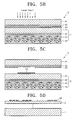
- FIG. 5A through 5D are cross-sectional views illustrating operations included in a method of manufacturing the electrophoretic display apparatus of FIG. 4 .
- a donor substrate 5 is prepared.
- the donor substrate 5 is manufactured by forming a light-to-heat conversion (LTHC) layer 52 on a donor substrate base 51, and then forming a color filter layer 53 on the LTHC layer 52.
- LTHC light-to-heat conversion
- the color filter layer 53 is arranged so as to face towards the second substrate base 21 of the second substrate 2.
- a laser beam is directed at on a region of the donor substrate 5 corresponding to a pixel.
- the laser beam is directed at on a region of the donor substrate 5 that will be aligned with a pixel electrode 17 when the electrophoretic display apparatus is fully manufactured.
- Light energy of the laser is converted to heat energy by the LTHC layer 52 to transcribe the color filter layer 53 onto the second substrate base 21.
- the laser is controlled to selectively irradiate each region where a color filter is to be formed.
- the donor substrate 5 is removed and the color filter 32 formed by transcription of the color filter layer 53 remains on the second substrate base 21.
- the second substrate 2, on which a plurality of color filters 32 are formed, and the first substrate 1, on which the thin film transistor is formed, are aligned and attached to each other.
- the color filters 32 are aligned with corresponding pixel electrodes 17.
- the thickness of the electrophoretic display apparatus can be decreased to increase the brightness of the electrophoretic display apparatus.
- the productivity of forming the electrophoretic display apparatus can be improved.
- FIG. 6A through 6D are cross-sectional views illustrating operations included in a method of manufacturing the electrophoretic display apparatus of FIG. 4 , according to another embodiment of the present invention.
- the first substrate 1 is attached to the second substrate 2.
- the structure of the second substrate 2 is the same structure as that illustrated in FIG. 2 , a detailed aligning operation is not required for attaching the first substrate 1 to the second substrate 2.
- the donor substrate 5 is formed, and then the donor substrate 5 is positioned on the second substrate base 21.
- the donor substrate 5 includes a donor substrate base 51, an LTHC layer 52 and a color filter layer 53.
- laser light is directed at a region corresponding to the pixel electrode 17 to transcribe the color filter layer 53 onto the second substrate base 21.
- a plurality of color filters can be formed on the second substrate base 21 by selectively irradiating each region where a color filter is to be formed.
- the donor substrate 5 is removed and the color filter 32 formed by the transcription of the color filter layer 53 remains on the second substrate base 21.
- a separate donor substrate 5 can be prepared for each color filter material.
- the operations of positioning the donor substrate 5, transcribing the color filter layer 53 and removing the donor substrate 5 may be carried out separately for each color filter material so that, as a non-limiting example, all of the red filters 32a are formed, then all of the green filters 32b, then all of the blue filters 32c.
- the method of manufacturing the electrophoretic display apparatus can be simple, and the productivity of forming the electrophoretic display apparatus can be improved.
- a full color electrophoretic display apparatus can be realized using a simple method.
- the productivity of forming the full color electrophoretic display apparatus can be improved.
Landscapes
- Physics & Mathematics (AREA)
- Nonlinear Science (AREA)
- Architecture (AREA)
- Civil Engineering (AREA)
- Structural Engineering (AREA)
- Optics & Photonics (AREA)
- General Physics & Mathematics (AREA)
- Engineering & Computer Science (AREA)
- Chemical & Material Sciences (AREA)
- Molecular Biology (AREA)
- Electrochemistry (AREA)
- Chemical Kinetics & Catalysis (AREA)
- Life Sciences & Earth Sciences (AREA)
- Health & Medical Sciences (AREA)
- Electrochromic Elements, Electrophoresis, Or Variable Reflection Or Absorption Elements (AREA)
Applications Claiming Priority (1)
| Application Number | Priority Date | Filing Date | Title |
|---|---|---|---|
| KR1020070002660A KR20080065486A (ko) | 2007-01-09 | 2007-01-09 | 전기 영동 디스플레이 장치 및 그 제조방법 |
Publications (1)
| Publication Number | Publication Date |
|---|---|
| EP1944649A1 true EP1944649A1 (en) | 2008-07-16 |
Family
ID=39272238
Family Applications (1)
| Application Number | Title | Priority Date | Filing Date |
|---|---|---|---|
| EP07252532A Withdrawn EP1944649A1 (en) | 2007-01-09 | 2007-06-22 | Electrophoretic display apparatus and manufacturing method thereof |
Country Status (5)
| Country | Link |
|---|---|
| US (1) | US7893918B2 (ja) |
| EP (1) | EP1944649A1 (ja) |
| JP (1) | JP2008170927A (ja) |
| KR (1) | KR20080065486A (ja) |
| CN (1) | CN101221338A (ja) |
Families Citing this family (11)
| Publication number | Priority date | Publication date | Assignee | Title |
|---|---|---|---|---|
| US7781784B2 (en) * | 2007-05-07 | 2010-08-24 | Samsung Electronics Co., Ltd. | Display apparatus with color pixels |
| JP5428211B2 (ja) * | 2008-06-13 | 2014-02-26 | セイコーエプソン株式会社 | 電気泳動表示装置の駆動方法 |
| KR101345172B1 (ko) * | 2008-07-18 | 2013-12-27 | 엘지디스플레이 주식회사 | 전기영동 표시소자 |
| KR101276749B1 (ko) * | 2009-08-03 | 2013-06-19 | 엘지디스플레이 주식회사 | 전기영동 표시장치 및 그 제조 방법 |
| TWI400549B (zh) * | 2010-06-01 | 2013-07-01 | Prime View Int Co Ltd | 彩色電泳顯示裝置之製造方法 |
| TWI547746B (zh) | 2010-07-13 | 2016-09-01 | 元太科技工業股份有限公司 | 顯示器 |
| CN102375281B (zh) * | 2010-08-17 | 2015-12-02 | 元太科技工业股份有限公司 | 显示器 |
| JP5817134B2 (ja) * | 2011-02-10 | 2015-11-18 | 凸版印刷株式会社 | 電気泳動表示装置の製造方法および電気泳動表示装置 |
| CN102654705A (zh) * | 2011-03-23 | 2012-09-05 | 京东方科技集团股份有限公司 | 一种电泳显示器组件及其制造方法 |
| CN103186006A (zh) * | 2011-12-29 | 2013-07-03 | 上海天马微电子有限公司 | 双面显示电子纸及电子纸显示器 |
| TWI490614B (zh) * | 2013-01-24 | 2015-07-01 | E Ink Holdings Inc | 電泳顯示裝置 |
Citations (6)
| Publication number | Priority date | Publication date | Assignee | Title |
|---|---|---|---|---|
| US20020050976A1 (en) * | 2000-11-02 | 2002-05-02 | Fuji Xerox Co., Ltd. | Image display medium, Image display device, and image display method |
| US20020105600A1 (en) * | 2000-12-01 | 2002-08-08 | Tatsuya Shimoda | Electrophoretic device, electronic sheet including the same, electronic book including the electronic sheet, and manufacturing method thereof |
| JP2004062040A (ja) | 2002-07-31 | 2004-02-26 | Seiko Epson Corp | 電気泳動装置の製造方法、電気泳動装置、電子機器 |
| KR20040053848A (ko) * | 2002-12-16 | 2004-06-25 | 삼성전자주식회사 | 유기 반도체 표시 장치 |
| US20040180275A1 (en) * | 2003-02-28 | 2004-09-16 | Sam-Yeoul Kim | Color filter transfer film and method of fabricating color filter panel for use in liquid crystal display device |
| WO2007063440A1 (en) * | 2005-11-29 | 2007-06-07 | Polymer Vision Limited | Color filter to prevent color errors in a roll up display |
Family Cites Families (30)
| Publication number | Priority date | Publication date | Assignee | Title |
|---|---|---|---|---|
| JP2575835B2 (ja) * | 1988-08-25 | 1997-01-29 | 富士通株式会社 | 拡大投写用液晶表示装置 |
| JPH0777687A (ja) * | 1993-09-10 | 1995-03-20 | Casio Comput Co Ltd | 液晶表示装置およびその製造方法 |
| KR100271487B1 (ko) * | 1997-05-23 | 2000-11-15 | 김순택 | 칼라필터용 도너필름 |
| US6031594A (en) * | 1998-03-12 | 2000-02-29 | Engle; Craig D. | Electro-optic device |
| JP4679726B2 (ja) * | 1998-10-07 | 2011-04-27 | イー インク コーポレイション | 非発光性電子ディスプレイ用照明システム |
| US6506438B2 (en) * | 1998-12-15 | 2003-01-14 | E Ink Corporation | Method for printing of transistor arrays on plastic substrates |
| AU2830200A (en) * | 1999-03-05 | 2000-09-28 | Seiko Epson Corporation | Electrophoresis display and its production method |
| JP3667242B2 (ja) * | 2000-04-13 | 2005-07-06 | キヤノン株式会社 | 電気泳動表示方法及び電気泳動表示装置 |
| JP4006925B2 (ja) * | 2000-05-30 | 2007-11-14 | セイコーエプソン株式会社 | 電気泳動表示装置の製造方法 |
| KR100346550B1 (ko) | 2000-06-13 | 2002-07-26 | 삼성에스디아이 주식회사 | 레이저 전사장치 |
| KR20030034820A (ko) | 2001-10-27 | 2003-05-09 | 삼성전자주식회사 | 반사-투과형 액정표시장치 및 그 제조방법 |
| JP2003270673A (ja) * | 2002-03-15 | 2003-09-25 | Toppan Printing Co Ltd | 表示パネル及び表示パネル用前面板 |
| US7388631B2 (en) * | 2002-10-10 | 2008-06-17 | Samsung Electronics, Co., Ltd. | Parallax compensating color filter and black mask for display apparatus |
| JP3941785B2 (ja) * | 2003-03-13 | 2007-07-04 | セイコーエプソン株式会社 | 膜形成方法およびカラーフィルタ基板の製造方法 |
| JP2005037851A (ja) * | 2003-06-24 | 2005-02-10 | Seiko Epson Corp | 電気泳動分散液、電気泳動表示装置、電気泳動表示装置の製造方法および電子機器 |
| US20050205999A1 (en) * | 2003-08-30 | 2005-09-22 | Visible Tech-Knowledgy, Inc. | Method for pattern metalization of substrates |
| US20050263903A1 (en) * | 2003-08-30 | 2005-12-01 | Visible Tech-Knowledgy, Inc. | Method for pattern metalization of substrates |
| JP2005114819A (ja) * | 2003-10-03 | 2005-04-28 | Toppan Printing Co Ltd | マイクロカプセル型電気泳動式表示パネル及びその製造方法 |
| KR20050068794A (ko) | 2003-12-30 | 2005-07-05 | 엘지.필립스 엘시디 주식회사 | 유기전계 발광소자와 그 제조방법 |
| JP4522101B2 (ja) * | 2004-01-27 | 2010-08-11 | キヤノン株式会社 | 電気泳動表示装置及び電気泳動表示装置の駆動方法 |
| KR100611767B1 (ko) | 2004-08-30 | 2006-08-10 | 삼성에스디아이 주식회사 | 레이저 전사용 도너 기판 및 그 필름을 사용하여 제조되는유기 전계 발광 소자의 제조 방법 |
| US7427441B2 (en) * | 2004-09-17 | 2008-09-23 | Eastman Kodak Co | Transparent polymeric coated conductor |
| US20060062983A1 (en) * | 2004-09-17 | 2006-03-23 | Irvin Glen C Jr | Coatable conductive polyethylenedioxythiophene with carbon nanotubes |
| US7825582B2 (en) * | 2004-11-08 | 2010-11-02 | Kyodo Printing Co., Ltd. | Flexible display and manufacturing method thereof |
| KR101133759B1 (ko) * | 2004-12-28 | 2012-04-09 | 삼성전자주식회사 | 전기 영동 표시 장치 및 그 제조 방법 |
| US7038833B1 (en) * | 2005-01-25 | 2006-05-02 | Xerox Corporation | Encapsulated bichromal balls |
| ATE389896T1 (de) | 2005-04-21 | 2008-04-15 | Samsung Sdi Germany Gmbh | Aktivmatrix-schaltung, aktivmatrix-anzeige und deren herstellungsverfahren |
| KR100953652B1 (ko) * | 2005-08-18 | 2010-04-20 | 삼성모바일디스플레이주식회사 | 유기 박막 트랜지스터 및 그 제조 방법 |
| JP5167624B2 (ja) * | 2005-12-28 | 2013-03-21 | セイコーエプソン株式会社 | 電気泳動表示装置及び電子機器 |
| US7572667B2 (en) * | 2006-01-20 | 2009-08-11 | Samsung Electronics Co., Ltd. | Method of forming an organic semiconductor pattern and method of manufacturing an organic thin film transistor using the same |
-
2007
- 2007-01-09 KR KR1020070002660A patent/KR20080065486A/ko not_active Application Discontinuation
- 2007-04-03 JP JP2007097312A patent/JP2008170927A/ja active Pending
- 2007-04-17 US US11/736,138 patent/US7893918B2/en active Active
- 2007-05-29 CN CNA2007101092833A patent/CN101221338A/zh active Pending
- 2007-06-22 EP EP07252532A patent/EP1944649A1/en not_active Withdrawn
Patent Citations (6)
| Publication number | Priority date | Publication date | Assignee | Title |
|---|---|---|---|---|
| US20020050976A1 (en) * | 2000-11-02 | 2002-05-02 | Fuji Xerox Co., Ltd. | Image display medium, Image display device, and image display method |
| US20020105600A1 (en) * | 2000-12-01 | 2002-08-08 | Tatsuya Shimoda | Electrophoretic device, electronic sheet including the same, electronic book including the electronic sheet, and manufacturing method thereof |
| JP2004062040A (ja) | 2002-07-31 | 2004-02-26 | Seiko Epson Corp | 電気泳動装置の製造方法、電気泳動装置、電子機器 |
| KR20040053848A (ko) * | 2002-12-16 | 2004-06-25 | 삼성전자주식회사 | 유기 반도체 표시 장치 |
| US20040180275A1 (en) * | 2003-02-28 | 2004-09-16 | Sam-Yeoul Kim | Color filter transfer film and method of fabricating color filter panel for use in liquid crystal display device |
| WO2007063440A1 (en) * | 2005-11-29 | 2007-06-07 | Polymer Vision Limited | Color filter to prevent color errors in a roll up display |
Also Published As
| Publication number | Publication date |
|---|---|
| CN101221338A (zh) | 2008-07-16 |
| JP2008170927A (ja) | 2008-07-24 |
| US7893918B2 (en) | 2011-02-22 |
| US20080165121A1 (en) | 2008-07-10 |
| KR20080065486A (ko) | 2008-07-14 |
Similar Documents
| Publication | Publication Date | Title |
|---|---|---|
| US7893918B2 (en) | Electrophoretic display apparatus and manufacturing method thereof | |
| US7286281B2 (en) | Electrophoretic display and method of manufacturing thereof | |
| KR100641376B1 (ko) | 박막 트랜지스터, 박막 트랜지스터의 제조 방법, 전자회로, 표시 장치 및 전자 기기 | |
| US8059329B2 (en) | Display substrate and method of manufacturing the same | |
| US7638802B2 (en) | Flat panel display including thin film transistor substrate | |
| JP2012054575A (ja) | 有機薄膜トランジスタ及びこれを備えた平板表示装置 | |
| JP2006330736A (ja) | 平板表示装置 | |
| CN101689510A (zh) | 半导体装置及其制造方法、显示装置及其制造方法 | |
| US9720292B2 (en) | Liquid crystal display panel and method for making same | |
| CN101714611A (zh) | 薄膜晶体管及其制造方法、和电子设备 | |
| EP2919267B1 (en) | Array substrate, manufacturing method therefor and display device | |
| US20070114525A1 (en) | Display device and manufacturing method | |
| US20150325815A1 (en) | Display device and manufacturing method of the same | |
| US8847207B2 (en) | Semiconductor device with bottom gate organic thin-film transistor, and display device and electronic equipment with same | |
| KR101427707B1 (ko) | 유기 박막 트랜지스터 기판 및 그의 제조 방법 | |
| JP2010224403A (ja) | アクティブマトリックス基板の製造方法、アクティブマトリックス基板、電気光学装置、および電子機器 | |
| US20160181556A1 (en) | Semiconductor device, method of manufacturing the same, and electronic apparatus | |
| US20090072225A1 (en) | Flat panel display device having organic thin film transistor and manufacturing method thereof | |
| JP2007235124A (ja) | パターン形成方法及びこれを利用した表示装置の製造方法 | |
| US9905581B2 (en) | Array substrate and display panel with same | |
| US20170176836A1 (en) | Display device and electronic apparatus | |
| US20160238918A1 (en) | Electrophoresis display apparatus, manufacturing method of electrophoresis display apparatus, and electronic device | |
| JP2007012669A (ja) | 薄膜トランジスタアレイとディスプレイ及び薄膜トランジスタアレイの製造方法 | |
| KR101785916B1 (ko) | 유기 박막트랜지스터 및 그 제조방법 그리고 이를 구비하는 액정표시장치 | |
| KR101924038B1 (ko) | 전기영동 표시장치와 이의 제조방법 |
Legal Events
| Date | Code | Title | Description |
|---|---|---|---|
| PUAI | Public reference made under article 153(3) epc to a published international application that has entered the european phase |
Free format text: ORIGINAL CODE: 0009012 |
|
| 17P | Request for examination filed |
Effective date: 20070628 |
|
| AK | Designated contracting states |
Kind code of ref document: A1 Designated state(s): AT BE BG CH CY CZ DE DK EE ES FI FR GB GR HU IE IS IT LI LT LU LV MC MT NL PL PT RO SE SI SK TR |
|
| AX | Request for extension of the european patent |
Extension state: AL BA HR MK RS |
|
| 17Q | First examination report despatched |
Effective date: 20081006 |
|
| RAP1 | Party data changed (applicant data changed or rights of an application transferred) |
Owner name: SAMSUNG MOBILE DISPLAY CO., LTD. |
|
| AKX | Designation fees paid |
Designated state(s): DE FR GB |
|
| STAA | Information on the status of an ep patent application or granted ep patent |
Free format text: STATUS: THE APPLICATION IS DEEMED TO BE WITHDRAWN |
|
| 18D | Application deemed to be withdrawn |
Effective date: 20120101 |